Embed Size (px)
Citation preview

Cambridge CMOS Sensors
is now
Member of the
ams Group
The technical content of this Cambridge CMOS Sensors (CCS) document is still valid.
Contact information:
Headquarters:
ams AG
Tobelbader Strasse 30
8141 Premstaetten, Austria
Tel: +43 (0) 3136 500 0
e-Mail: [email protected]
Please visit our website at www.ams.com
CC-000803-AN revision: 6
CCS811 Programming and Interfacing Guide
P a g e | 1 © Cambridge CMOS Sensors Ltd, Deanland House, Cowley Road, Cambridge, CB4 0DL, UK
Confidential http://www.ccmoss.com Date Issued: 25 May 2016
CCS811 Programming and Interfacing Guide
Introduction
This application note details the programming model and recommended interfacing techniques for Cambridge CMOS Sensor’s CCS811 digital gas sensor. It is intended for software developers who will integrate the CCS811 device into an environment with another core (such as a sensor hub, sensor aggregator, phone, tablet or digital display product). It details how user software can interface to, control, enable and disable the sensor.
CCS811 Device Hardware Overview
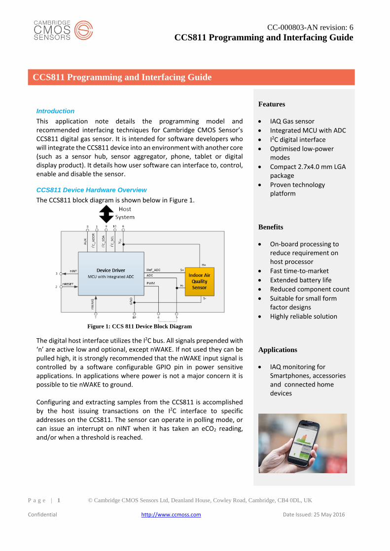
The CCS811 block diagram is shown below in Figure 1.
Figure 1: CCS 811 Device Block Diagram
The digital host interface utilizes the I2C bus. All signals prepended with ‘n’ are active low and optional, except nWAKE. If not used they can be pulled high, it is strongly recommended that the nWAKE input signal is controlled by a software configurable GPIO pin in power sensitive applications. In applications where power is not a major concern it is possible to tie nWAKE to ground. Configuring and extracting samples from the CCS811 is accomplished by the host issuing transactions on the I2C interface to specific addresses on the CCS811. The sensor can operate in polling mode, or can issue an interrupt on nINT when it has taken an eCO2 reading, and/or when a threshold is reached.
Features
IAQ Gas sensor
Integrated MCU with ADC
I2C digital interface
Optimised low-power modes
Compact 2.7x4.0 mm LGA package
Proven technology platform
Benefits
On-board processing to reduce requirement on host processor
Fast time-to-market
Extended battery life
Reduced component count
Suitable for small form factor designs
Highly reliable solution
Applications
IAQ monitoring for Smartphones, accessories and connected home devices
CC-000803-AN revision: 6
CCS811 Programming and Interfacing Guide
P a g e | 2 © Cambridge CMOS Sensors Ltd, Deanland House, Cowley Road, Cambridge, CB4 0DL, UK
Confidential http://www.ccmoss.com Date Issued: 25 May 2016
Programming Model
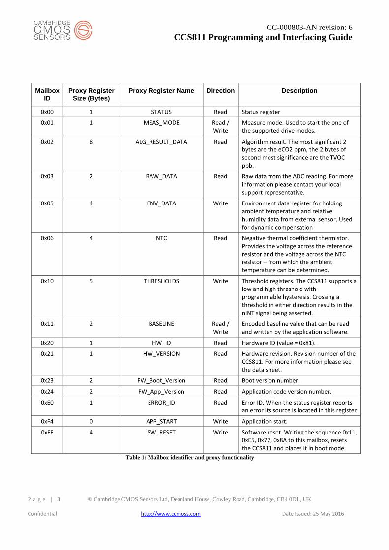
For flexibility and software driver maintenance simplification the CCS811 does not support direct addressing of registers over the I2C bus. Instead it supports single byte mailboxes that behave as proxies for registers with specific functionality and data sizes. To access a register an I2C transaction must be issued with the target address on the CCS811 being equal to the intended mailbox. All I2C transactions must use the 7-bit address 0x5A (I2C _ADDR low) or 0x5B (I2C _ADDR high) when writing to and reading from the CCS811. Table 1 shows the register map for CCS811.
CC-000803-AN revision: 6
CCS811 Programming and Interfacing Guide
P a g e | 3 © Cambridge CMOS Sensors Ltd, Deanland House, Cowley Road, Cambridge, CB4 0DL, UK
Confidential http://www.ccmoss.com Date Issued: 25 May 2016
Mailbox ID
Proxy Register Size (Bytes)
Proxy Register Name Direction Description
0x00 1 STATUS Read Status register
0x01 1 MEAS_MODE Read / Write
Measure mode. Used to start the one of the supported drive modes.
0x02 8 ALG_RESULT_DATA Read Algorithm result. The most significant 2 bytes are the eCO2 ppm, the 2 bytes of second most significance are the TVOC ppb.
0x03 2 RAW_DATA Read Raw data from the ADC reading. For more information please contact your local support representative.
0x05 4 ENV_DATA Write Environment data register for holding ambient temperature and relative humidity data from external sensor. Used for dynamic compensation
0x06 4 NTC Read Negative thermal coefficient thermistor. Provides the voltage across the reference resistor and the voltage across the NTC resistor – from which the ambient temperature can be determined.
0x10 5 THRESHOLDS Write Threshold registers. The CCS811 supports a low and high threshold with programmable hysteresis. Crossing a threshold in either direction results in the nINT signal being asserted.
0x11 2 BASELINE Read / Write
Encoded baseline value that can be read and written by the application software.
0x20 1 HW_ID Read Hardware ID (value = 0x81).
0x21 1 HW_VERSION Read Hardware revision. Revision number of the CCS811. For more information please see the data sheet.
0x23 2 FW_Boot_Version Read Boot version number.
0x24 2 FW_App_Version Read Application code version number.
0xE0 1 ERROR_ID Read Error ID. When the status register reports an error its source is located in this register
0xF4 0 APP_START Write Application start.
0xFF 4 SW_RESET Write Software reset. Writing the sequence 0x11, 0xE5, 0x72, 0x8A to this mailbox, resets the CCS811 and places it in boot mode.
Table 1: Mailbox identifier and proxy functionality
CC-000803-AN revision: 6
CCS811 Programming and Interfacing Guide
P a g e | 4 © Cambridge CMOS Sensors Ltd, Deanland House, Cowley Road, Cambridge, CB4 0DL, UK
Confidential http://www.ccmoss.com Date Issued: 25 May 2016
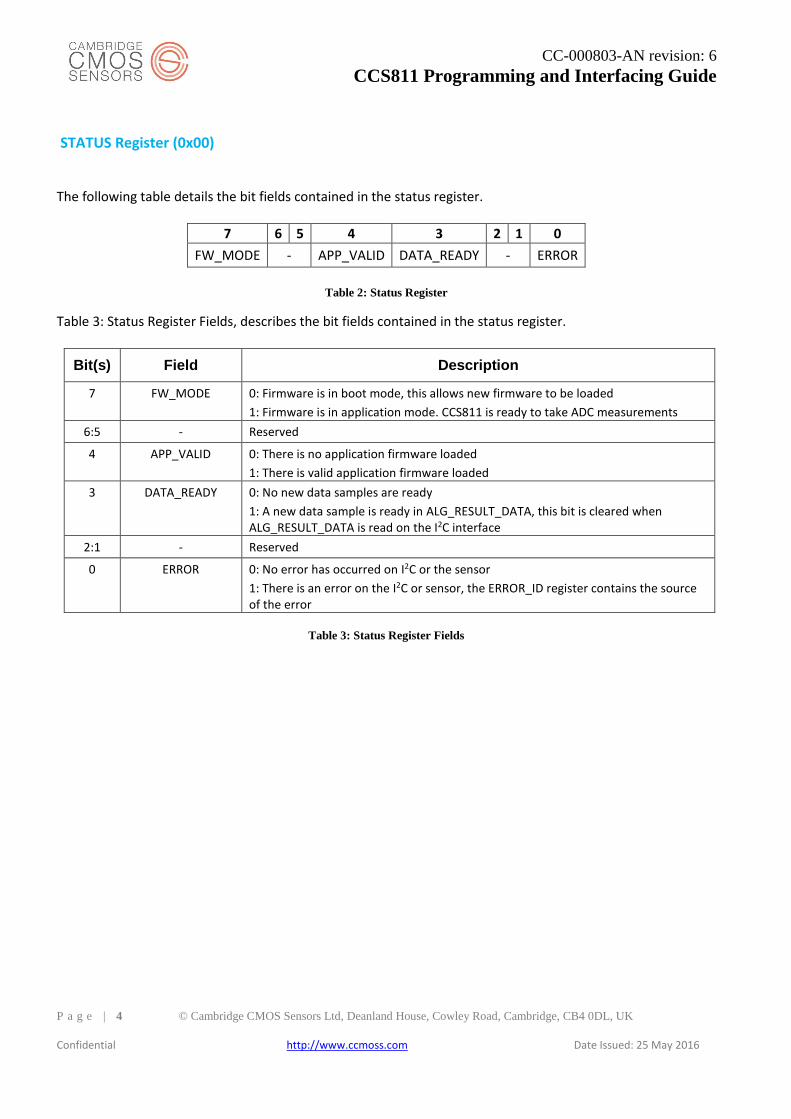
STATUS Register (0x00)
The following table details the bit fields contained in the status register.
7 6 5 4 3 2 1 0
FW_MODE - APP_VALID DATA_READY - ERROR
Table 2: Status Register
Table 3: Status Register Fields, describes the bit fields contained in the status register.
Bit(s) Field Description
7 FW_MODE 0: Firmware is in boot mode, this allows new firmware to be loaded
1: Firmware is in application mode. CCS811 is ready to take ADC measurements
6:5 - Reserved
4 APP_VALID 0: There is no application firmware loaded
1: There is valid application firmware loaded
3 DATA_READY 0: No new data samples are ready
1: A new data sample is ready in ALG_RESULT_DATA, this bit is cleared when ALG_RESULT_DATA is read on the I2C interface
2:1 - Reserved
0 ERROR 0: No error has occurred on I2C or the sensor
1: There is an error on the I2C or sensor, the ERROR_ID register contains the source of the error
Table 3: Status Register Fields
CC-000803-AN revision: 6
CCS811 Programming and Interfacing Guide
P a g e | 5 © Cambridge CMOS Sensors Ltd, Deanland House, Cowley Road, Cambridge, CB4 0DL, UK
Confidential http://www.ccmoss.com Date Issued: 25 May 2016
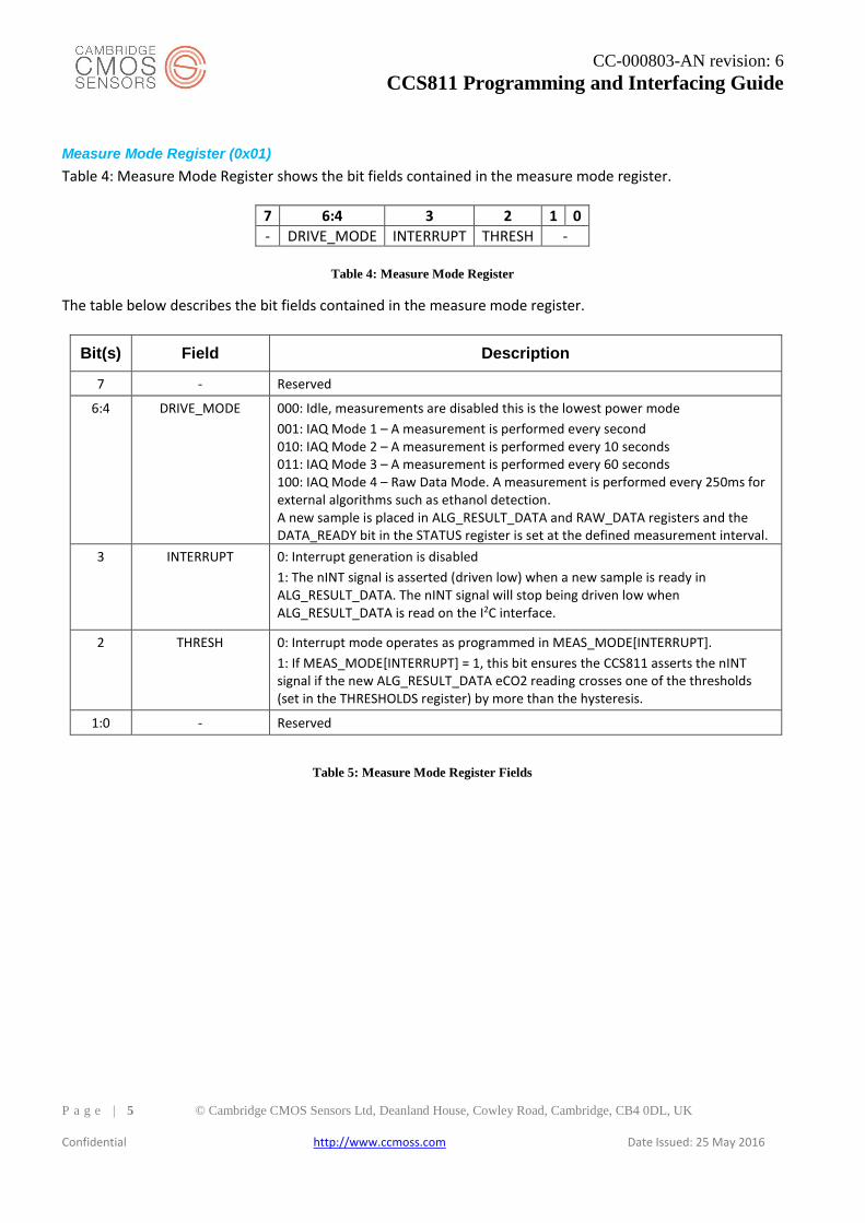
Measure Mode Register (0x01)
Table 4: Measure Mode Register shows the bit fields contained in the measure mode register.
7 6:4 3 2 1 0
- DRIVE_MODE INTERRUPT THRESH -
Table 4: Measure Mode Register
The table below describes the bit fields contained in the measure mode register.
Bit(s) Field Description
7 - Reserved
6:4 DRIVE_MODE 000: Idle, measurements are disabled this is the lowest power mode
001: IAQ Mode 1 – A measurement is performed every second 010: IAQ Mode 2 – A measurement is performed every 10 seconds 011: IAQ Mode 3 – A measurement is performed every 60 seconds 100: IAQ Mode 4 – Raw Data Mode. A measurement is performed every 250ms for external algorithms such as ethanol detection. A new sample is placed in ALG_RESULT_DATA and RAW_DATA registers and the DATA_READY bit in the STATUS register is set at the defined measurement interval.
3 INTERRUPT 0: Interrupt generation is disabled
1: The nINT signal is asserted (driven low) when a new sample is ready in ALG_RESULT_DATA. The nINT signal will stop being driven low when ALG_RESULT_DATA is read on the I2C interface.
2 THRESH 0: Interrupt mode operates as programmed in MEAS_MODE[INTERRUPT].
1: If MEAS_MODE[INTERRUPT] = 1, this bit ensures the CCS811 asserts the nINT signal if the new ALG_RESULT_DATA eCO2 reading crosses one of the thresholds (set in the THRESHOLDS register) by more than the hysteresis.
1:0 - Reserved
Table 5: Measure Mode Register Fields
CC-000803-AN revision: 6
CCS811 Programming and Interfacing Guide
P a g e | 6 © Cambridge CMOS Sensors Ltd, Deanland House, Cowley Road, Cambridge, CB4 0DL, UK
Confidential http://www.ccmoss.com Date Issued: 25 May 2016
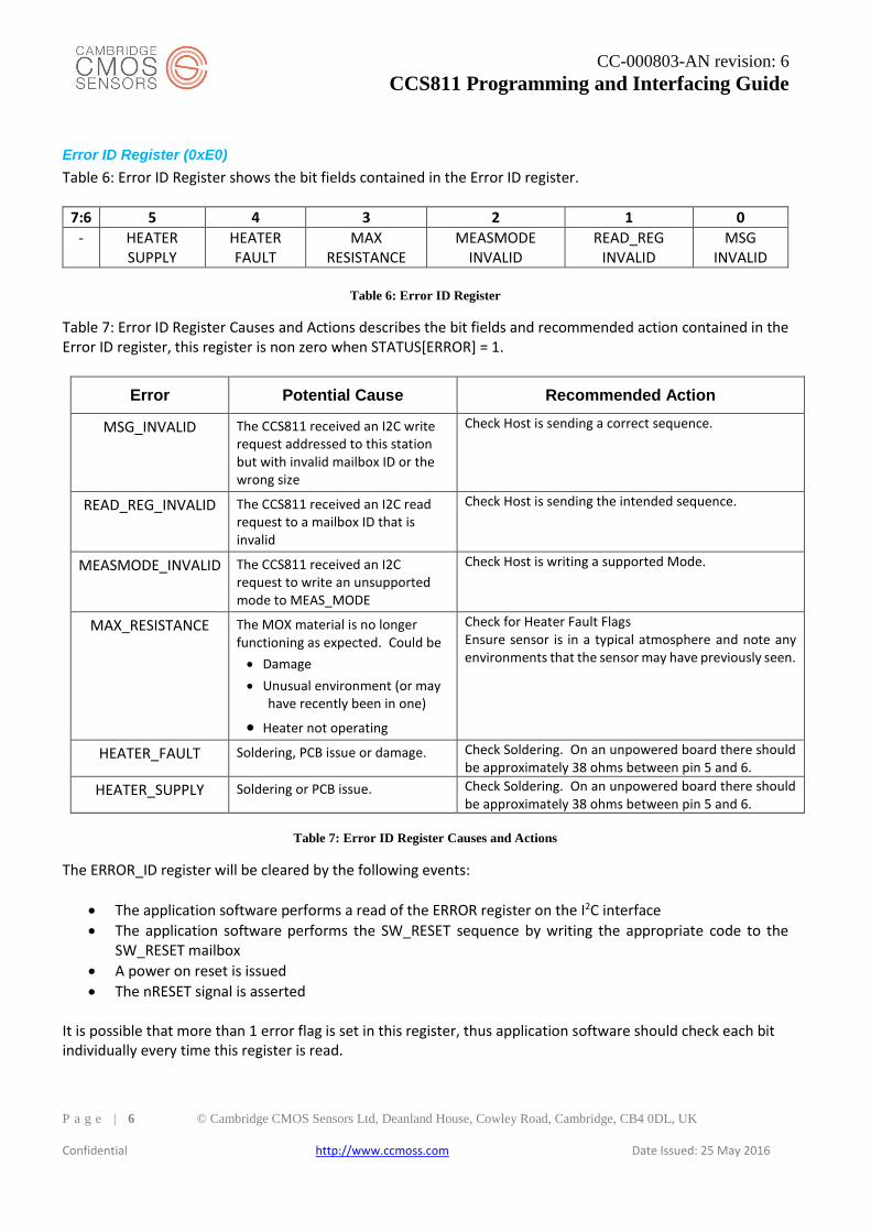
Error ID Register (0xE0)
Table 6: Error ID Register shows the bit fields contained in the Error ID register.
7:6 5 4 3 2 1 0
- HEATER SUPPLY
HEATER FAULT
MAX RESISTANCE
MEASMODE INVALID
READ_REG INVALID
MSG INVALID
Table 6: Error ID Register
Table 7: Error ID Register Causes and Actions describes the bit fields and recommended action contained in the Error ID register, this register is non zero when STATUS[ERROR] = 1.
Error Potential Cause Recommended Action
MSG_INVALID The CCS811 received an I2C write request addressed to this station but with invalid mailbox ID or the wrong size
Check Host is sending a correct sequence.
READ_REG_INVALID The CCS811 received an I2C read request to a mailbox ID that is invalid
Check Host is sending the intended sequence.
MEASMODE_INVALID The CCS811 received an I2C request to write an unsupported mode to MEAS_MODE
Check Host is writing a supported Mode.
MAX_RESISTANCE The MOX material is no longer functioning as expected. Could be
Damage
Unusual environment (or may have recently been in one)
Heater not operating
Check for Heater Fault Flags Ensure sensor is in a typical atmosphere and note any environments that the sensor may have previously seen.
HEATER_FAULT Soldering, PCB issue or damage. Check Soldering. On an unpowered board there should be approximately 38 ohms between pin 5 and 6.
HEATER_SUPPLY Soldering or PCB issue. Check Soldering. On an unpowered board there should be approximately 38 ohms between pin 5 and 6.
Table 7: Error ID Register Causes and Actions
The ERROR_ID register will be cleared by the following events:
The application software performs a read of the ERROR register on the I2C interface
The application software performs the SW_RESET sequence by writing the appropriate code to the SW_RESET mailbox
A power on reset is issued
The nRESET signal is asserted It is possible that more than 1 error flag is set in this register, thus application software should check each bit individually every time this register is read.
CC-000803-AN revision: 6
CCS811 Programming and Interfacing Guide
P a g e | 7 © Cambridge CMOS Sensors Ltd, Deanland House, Cowley Road, Cambridge, CB4 0DL, UK
Confidential http://www.ccmoss.com Date Issued: 25 May 2016
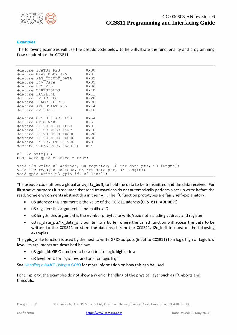
Examples
The following examples will use the pseudo code below to help illustrate the functionality and programming flow required for the CCS811.
#define STATUS_REG 0x00
#define MEAS_MODE_REG 0x01
#define ALG_RESULT_DATA 0x02
#define ENV_DATA 0x05
#define NTC_REG 0x06
#define THRESHOLDS 0x10
#define BASELINE 0x11
#define HW_ID_REG 0x20
#define ERROR_ID_REG 0xE0
#define APP_START_REG 0xF4
#define SW_RESET 0xFF
#define CCS_811_ADDRESS 0x5A
#define GPIO_WAKE 0x5
#define DRIVE_MODE_IDLE 0x0
#define DRIVE_MODE_1SEC 0x10
#define DRIVE_MODE_10SEC 0x20
#define DRIVE_MODE_60SEC 0x30
#define INTERRUPT_DRIVEN 0x8
#define THRESHOLDS_ENABLED 0x4
u8 i2c_buff[8];
bool wake_gpio_enabled = true;
void i2c_write(u8 address, u8 register, u8 *tx_data_ptr, u8 length);
void i2c_read(u8 address, u8 *rx_data_ptr, u8 length);
void gpio_write(u8 gpio_id, u8 level);
The pseudo code utilizes a global array, i2c_buff, to hold the data to be transmitted and the data received. For illustrative purposes it is assumed that read transactions do not automatically perform a set-up write before the read. Some environments abstract this in their API. The I2C function prototypes are fairly self-explanatory:
u8 address: this argument is the value of the CCS811 address (CCS_811_ADDRESS)
u8 register: this argument is the mailbox ID
u8 length: this argument is the number of bytes to write/read not including address and register
u8 rx_data_ptr/tx_data_ptr: pointer to a buffer where the called function will access the data to be written to the CCS811 or store the data read from the CCS811, i2c_buff in most of the following examples
The gpio_write function is used by the host to write GPIO outputs (input to CCS811) to a logic high or logic low level. Its arguments are described below:
u8 gpio_id: GPIO number to be written to logic high or low
u8 level: zero for logic low, and one for logic high
See Handling nWAKE Using a GPIO for more information on how this can be used.
For simplicity, the examples do not show any error handling of the physical layer such as I2C aborts and timeouts.
CC-000803-AN revision: 6
CCS811 Programming and Interfacing Guide
P a g e | 8 © Cambridge CMOS Sensors Ltd, Deanland House, Cowley Road, Cambridge, CB4 0DL, UK
Confidential http://www.ccmoss.com Date Issued: 25 May 2016
CCS811 I2C Data Byte Ordering
When reading or writing more than one byte the user must be aware of the order of the bytes used by the CCS811. The CCS811 assumes that the most significant byte of the scalar is present on the I2C before bytes of lesser significance. For example reading a 16-bit scalar with the value 0x11AA, the byte with value 0x11 would appear on the bus before the byte with value 0xAA.
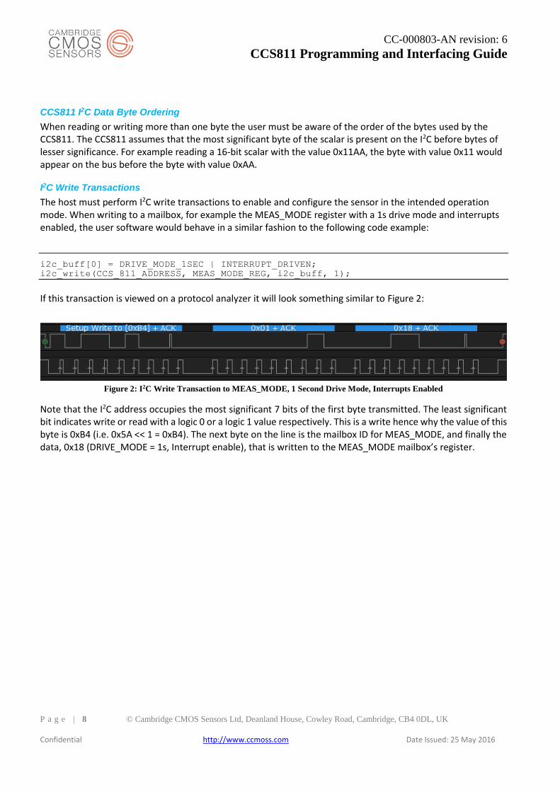
I2C Write Transactions
The host must perform I2C write transactions to enable and configure the sensor in the intended operation mode. When writing to a mailbox, for example the MEAS_MODE register with a 1s drive mode and interrupts enabled, the user software would behave in a similar fashion to the following code example:
i2c_buff[0] = DRIVE_MODE_1SEC | INTERRUPT_DRIVEN;
i2c_write(CCS_811_ADDRESS, MEAS_MODE_REG, i2c_buff, 1);
If this transaction is viewed on a protocol analyzer it will look something similar to Figure 2:
Figure 2: I2C Write Transaction to MEAS_MODE, 1 Second Drive Mode, Interrupts Enabled
Note that the I2C address occupies the most significant 7 bits of the first byte transmitted. The least significant bit indicates write or read with a logic 0 or a logic 1 value respectively. This is a write hence why the value of this byte is 0xB4 (i.e. 0x5A << 1 = 0xB4). The next byte on the line is the mailbox ID for MEAS_MODE, and finally the data, 0x18 (DRIVE_MODE = 1s, Interrupt enable), that is written to the MEAS_MODE mailbox’s register.
CC-000803-AN revision: 6
CCS811 Programming and Interfacing Guide
P a g e | 9 © Cambridge CMOS Sensors Ltd, Deanland House, Cowley Road, Cambridge, CB4 0DL, UK
Confidential http://www.ccmoss.com Date Issued: 25 May 2016
I2C Read Transactions
I2C read transactions must be preceded with a set-up write to enable the target mailbox for the read. This is best illustrated by an example. Let’s assume that the user is required to read the STATUS register, the code flow would look like the following:
i2c_write(CCS_811_ADDRESS, STATUS_REG, i2c_buff, 0);
i2c_read(CCS_811_ADDRESS, i2c_buff, 1);
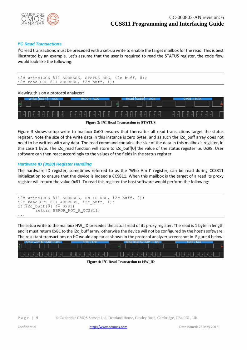
Viewing this on a protocol analyzer:
Figure 3: I2C Read Transaction to STATUS
Figure 3 shows setup write to mailbox 0x00 ensures that thereafter all read transactions target the status register. Note the size of the write data in this instance is zero bytes, and as such the i2c_buff array does not need to be written with any data. The read command contains the size of the data in this mailbox’s register, in this case 1 byte. The i2c_read function will store to i2c_buff[0] the value of the status register i.e. 0x98. User software can then react accordingly to the values of the fields in the status register.
Hardware ID (0x20) Register Handling
The hardware ID register, sometimes referred to as the ‘Who Am I’ register, can be read during CCS811 initialization to ensure that the device is indeed a CCS811. When this mailbox is the target of a read its proxy register will return the value 0x81. To read this register the host software would perform the following:
i2c_write(CCS_811_ADDRESS, HW_ID_REG, i2c_buff, 0);
i2c_read(CCS_811_ADDRESS, i2c_buff, 1);
if(i2c_buff[0] != 0x81)
return ERROR_NOT_A_CCS811;
...
The setup write to the mailbox HW_ID precedes the actual read of its proxy register. The read is 1 byte in length and it must return 0x81 to the i2c_buff array, otherwise the device will not be configured by the host’s software. The resultant transactions on I2C would appear as shown in the protocol analyzer screenshot in Figure 4 below:
Figure 4: I2C Read Transaction to HW_ID
CC-000803-AN revision: 6
CCS811 Programming and Interfacing Guide
P a g e | 1 0 © Cambridge CMOS Sensors Ltd, Deanland House, Cowley Road, Cambridge, CB4 0DL, UK
Confidential http://www.ccmoss.com Date Issued: 25 May 2016
APP_START (0xF4) Handling
The mailbox ID 0xF4, APP_START, is used to transition the CCS811 state from boot to application mode. Note that the size of the proxy register for this mailbox is zero bytes. Therefore to trigger this state transition a setup write with no data is all that is required. A typical flow can be viewed below:
i2c_write(CCS_811_ADDRESS, STATUS_REG, i2c_buff, 0);
i2c_read(CCS_811_ADDRESS, i2c_buff, 1);
if(!(i2c_buff[0] & 0x10))
return ERROR_NO_VALID_APP;
i2c_write(CCS_811_ADDRESS, APP_START_REG, i2c_buff, 0);
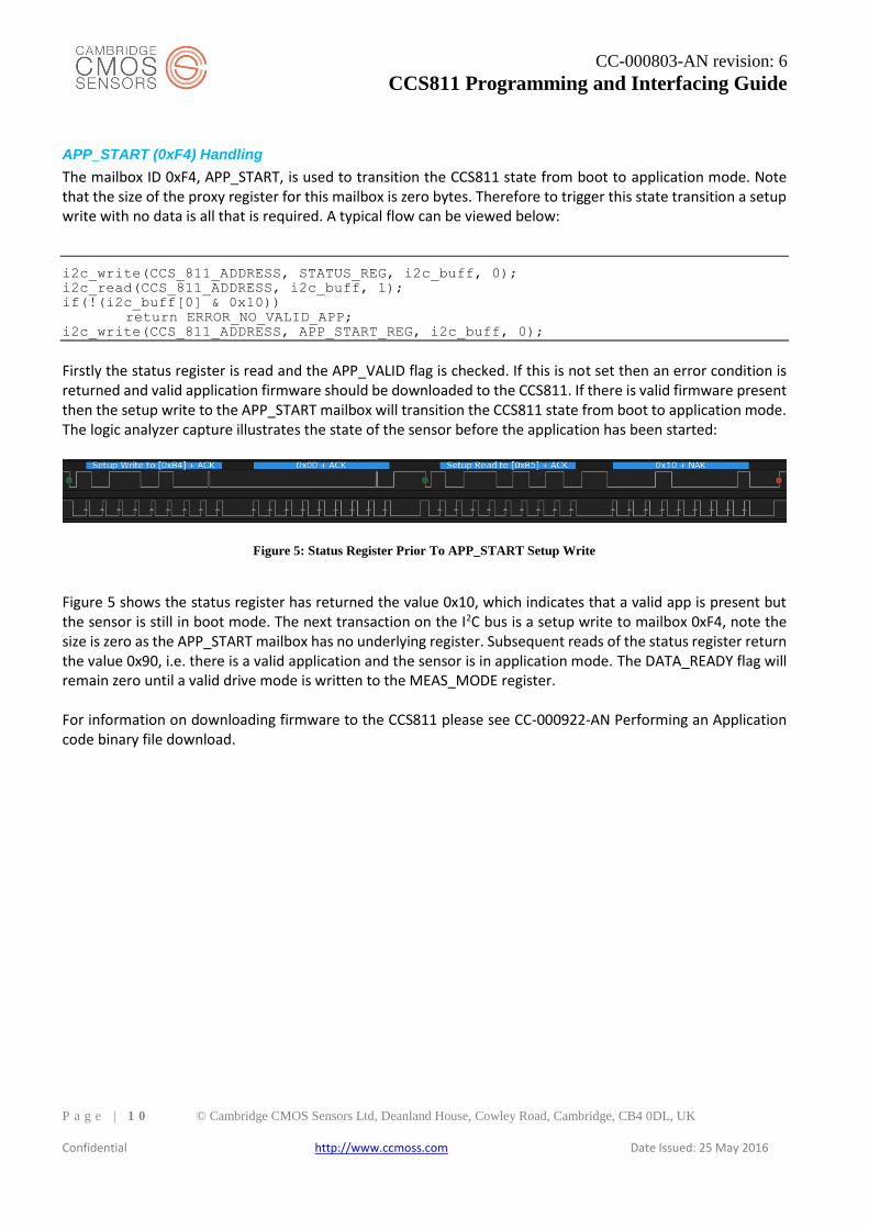
Firstly the status register is read and the APP_VALID flag is checked. If this is not set then an error condition is returned and valid application firmware should be downloaded to the CCS811. If there is valid firmware present then the setup write to the APP_START mailbox will transition the CCS811 state from boot to application mode. The logic analyzer capture illustrates the state of the sensor before the application has been started:
Figure 5: Status Register Prior To APP_START Setup Write
Figure 5 shows the status register has returned the value 0x10, which indicates that a valid app is present but the sensor is still in boot mode. The next transaction on the I2C bus is a setup write to mailbox 0xF4, note the size is zero as the APP_START mailbox has no underlying register. Subsequent reads of the status register return the value 0x90, i.e. there is a valid application and the sensor is in application mode. The DATA_READY flag will remain zero until a valid drive mode is written to the MEAS_MODE register. For information on downloading firmware to the CCS811 please see CC-000922-AN Performing an Application code binary file download.
CC-000803-AN revision: 6
CCS811 Programming and Interfacing Guide
P a g e | 1 1 © Cambridge CMOS Sensors Ltd, Deanland House, Cowley Road, Cambridge, CB4 0DL, UK
Confidential http://www.ccmoss.com Date Issued: 25 May 2016
Host Software Polling Mode
One mode of operation for the sensor is polling mode. In this mode the host software is required to cyclically read data from the sensor at the same period as the programmed drive mode. A timer interrupt on the host application can be used to read the sensor’s eCO2 and TVOC values. A typical flow for this can be seen below:
u8 *timer_routine_read_data(){
i2c_write(CCS_811_ADDRESS, STATUS_REG, i2c_buff, 0);
i2c_read(CCS_811_ADDRESS, i2c_buff, 1);
if(i2c_buff & 0x8) // check if data ready
{
i2c_write(CCS_811_ADDRESS, ALG_RESULT_DATA, i2c_buff, 0);
i2c_read(CCS_811_ADDRESS, i2c_buff, 4);
}
return i2c_buff;
}
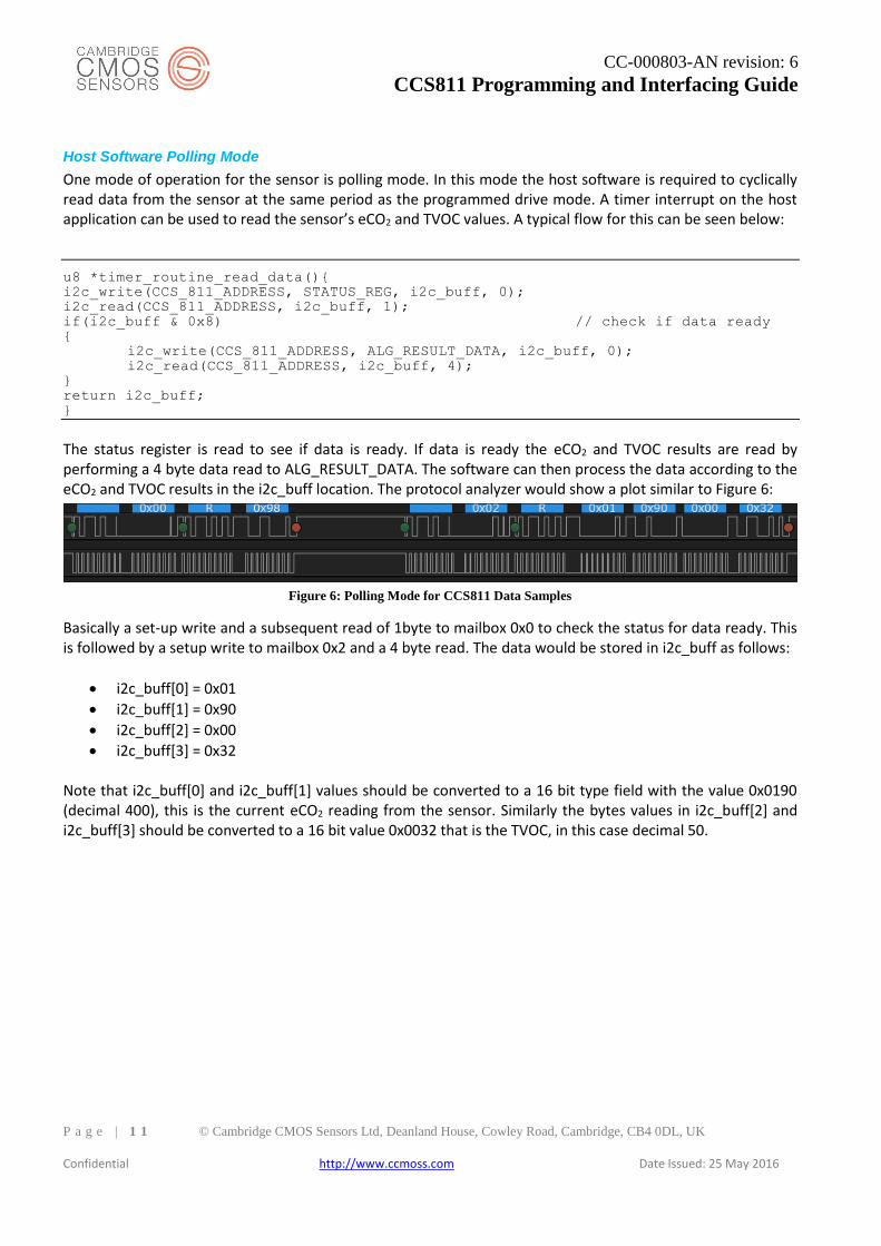
The status register is read to see if data is ready. If data is ready the eCO2 and TVOC results are read by performing a 4 byte data read to ALG_RESULT_DATA. The software can then process the data according to the eCO2 and TVOC results in the i2c_buff location. The protocol analyzer would show a plot similar to Figure 6:
Figure 6: Polling Mode for CCS811 Data Samples
Basically a set-up write and a subsequent read of 1byte to mailbox 0x0 to check the status for data ready. This is followed by a setup write to mailbox 0x2 and a 4 byte read. The data would be stored in i2c_buff as follows:
i2c_buff[0] = 0x01
i2c_buff[1] = 0x90
i2c_buff[2] = 0x00
i2c_buff[3] = 0x32 Note that i2c_buff[0] and i2c_buff[1] values should be converted to a 16 bit type field with the value 0x0190 (decimal 400), this is the current eCO2 reading from the sensor. Similarly the bytes values in i2c_buff[2] and i2c_buff[3] should be converted to a 16 bit value 0x0032 that is the TVOC, in this case decimal 50.
CC-000803-AN revision: 6
CCS811 Programming and Interfacing Guide
P a g e | 1 2 © Cambridge CMOS Sensors Ltd, Deanland House, Cowley Road, Cambridge, CB4 0DL, UK
Confidential http://www.ccmoss.com Date Issued: 25 May 2016
This example assumes 4 bytes of data is read from ALG_RESULT_DATA. It is possible to read up to eight bytes from ALG_RESULT_DATA. The format of this is shown in Table 8: ALG_RESULT_DATA Format.
Byte: 0:1 2:3 4 5 6:7
Parameter: ECO2 TVOC STATUS ERROR_ID RAW_DATA
Table 8: ALG_RESULT_DATA Format
The user can define a structure to hold this data as follows: typedef struct {
u16 eco2;
u16 tvoc;
u8 status;
u8 error_id;
u16 raw_data;
} ccs811_measurement_t;
The base address of this structure can be cast to a char pointer and supplied as the address that the i2c_read routine deposits the data read from the sensor. Alternatively data can be copied to this structure from the current i2c_buff. Care must always be taken with processor endianness when accessing data written to the i2c_buff by the i2c_read function.
Reading Data On Interrupt Thresholds Disabled
The nINT signal is driven low by the CCS811 whenever new data is ready and the MEAS_MODE[INTERRUPT] bit is set. The host’s CCS811 driver can provide a callback, to the host application’s O/S, which is registered to the GPIO signal connected to the nINT output signal. When the nINT is asserted the callback is called which then reads the ALG_RESULT_DATA from the CCS811:
u8 *ccs811_read_data_callback(){
i2c_write(CCS_811_ADDRESS, ALG_RESULT_DATA, i2c_buff, 0);
i2c_read(CCS_811_ADDRESS, i2c_buff, 4);
return i2c_buff;
}
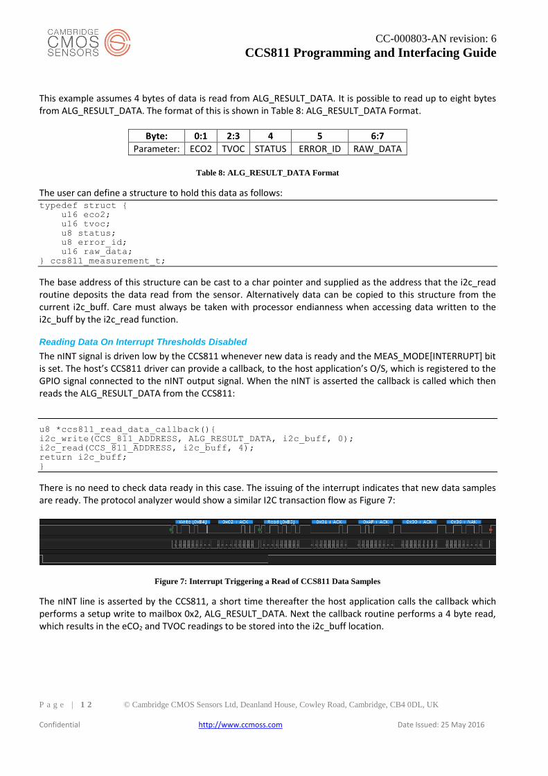
There is no need to check data ready in this case. The issuing of the interrupt indicates that new data samples are ready. The protocol analyzer would show a similar I2C transaction flow as Figure 7:
Figure 7: Interrupt Triggering a Read of CCS811 Data Samples
The nINT line is asserted by the CCS811, a short time thereafter the host application calls the callback which performs a setup write to mailbox 0x2, ALG_RESULT_DATA. Next the callback routine performs a 4 byte read, which results in the eCO2 and TVOC readings to be stored into the i2c_buff location.
CC-000803-AN revision: 6
CCS811 Programming and Interfacing Guide
P a g e | 1 3 © Cambridge CMOS Sensors Ltd, Deanland House, Cowley Road, Cambridge, CB4 0DL, UK
Confidential http://www.ccmoss.com Date Issued: 25 May 2016
Reading Data On Threshold Interrupt
It is possible to program CCS811 such that the nINT signal generates an interrupt when an eCO2 reading crosses the low or high threshold in either direction. The firmware will only trigger the interrupt if the threshold is breached by more than a programmable hysteresis value.
typedef struct __packed{
u16 thresh_low;
u16 thresh_high;
u8 thresh_hyst;
}threshold_reg;
...
threshold_reg thresh_reg = {1000, 2200, 50};
temp_ptr = (uint8_t *)&thresh_reg->thresh_low;
i2c_write(CCS_811_ADDRESS, THRESHOLDS, temp_ptr, 5);
...
i2c_buff[0] = DRIVE_MODE_1SEC | INTERRUPT_DRIVEN | THRESHOLDS_ENABLED;
i2c_write(CCS_811_ADDRESS, MEAS_MODE_REG, i2c_buff, 1);
Before enabling the drive mode the user must program the desired low and high threshold value in the THRESHOLDS’ registers. This can be achieved by defining and declaring the structure threshold_reg shown above. It can be used to hold the values of the threshold registers. The structure’s base can be cast to a pointer to char, it then can be the tx_data_ptr argument in the i2c_write function call. The default values in the CCS811 threshold registers are as follows, if the application always uses these values there is no requirement to write to the threshold registers:
LOW_THRESHOLD = 1500ppm
HIGH_THRESHOLD = 2500ppm
HYSTERESIS = 50ppm
If only one threshold is required the low and high threshold can be configured to the same value. It is possible to change the threshold registers on the fly.
CC-000803-AN revision: 6
CCS811 Programming and Interfacing Guide
P a g e | 1 4 © Cambridge CMOS Sensors Ltd, Deanland House, Cowley Road, Cambridge, CB4 0DL, UK
Confidential http://www.ccmoss.com Date Issued: 25 May 2016
Handling nWAKE Using a GPIO
There are 2 methods for handling the nWAKE:
1. Pull low and therefore always asserted* 2. Use a GPIO and control assertion and deassertion dynamically
When the active low nWAKE signal is asserted the CCS811 integrated processor is active and will handle requests on the I2C interface. When this pin is logic high the CCS811 enters sleep mode and all I2C requests are ignored. Therefore when this signal is dynamically controlled by a GPIO it can efficiently control CCS811 power consumption. Pulling nWAKE permanently low is not recommended in power sensitive applications.
if(wake_gpio_enabled)
gpio_write(GPIO_WAKE, 0); // enable wake
i2c_write(CCS_811_ADDRESS, STATUS_REG, i2c_buff, 0);
i2c_read(CCS_811_ADDRESS, i2c_buff, 1);
if(i2c_buff & 0x8) // check if data ready
{
i2c_write(CCS_811_ADDRESS, ALG_RESULT_DATA, i2c_buff, 0);
i2c_read(CCS_811_ADDRESS, i2c_buff, 4);
}
if(wake_gpio_enabled)
gpio_write(GPIO_WAKE, 1); // disable wake
Firstly nWAKE is enabled by writing logic level zero to the GPIO, note the code checks if this signal is currently controlled by a GPIO. If no GPIO is available then nWAKE must be pulled low. The status register is then read to see if data is ready.
When data is ready the eCO2 and TVOC results are read by performing a read to ALG_RESULT_DATA. Finally nWAKE is disabled. The software can then process the data according to the eCO2 and TVOC results in the i2c_buff location.
CC-000803-AN revision: 6
CCS811 Programming and Interfacing Guide
P a g e | 1 5 © Cambridge CMOS Sensors Ltd, Deanland House, Cowley Road, Cambridge, CB4 0DL, UK
Confidential http://www.ccmoss.com Date Issued: 25 May 2016
Disabling the CCS811
In order to disable the sensor and place in the lowest possible power consumption mode (while still connected to the supply voltage VDD), the following can used:
if(wake_gpio_enabled)
gpio_write(GPIO_WAKE, 0); // enable wake
i2c_buff[0] = DRIVE_MODE_IDLE;
i2c_write(CCS_811_ADDRESS, MEAS_MODE_REG, i2c_buff, 1);
if(wake_gpio_enabled)
gpio_write(GPIO_WAKE, 1); // disable wake
Basically the driver code should disable the readings from the sensor by placing the drive mode in MEAS_MODE in the idle state. The nWAKE signal can then be placed in its inactive state, thus no I2C commands will be processed. To ‘re-awaken’ the sensor nWAKE should be asserted and the appropriate drive mode including interrupt, if used, should be written to the MEAS_MODE register.
Another method of disabling the sensor is by writing the reset unlock sequence to the SW_RESET mailbox. This sequence is shown in the code example below (nWAKE handling not shown for simplicity):
u8 soft_reset_code[] = {0x11, 0xE5, 0x72, 0x8A};
i2c_write(CCS_811_ADDRESS, SW_RESET, soft_reset_code, 4);
This will reset the CCS811 and place it in boot mode, ready to be reprogrammed.
CC-000803-AN revision: 6
CCS811 Programming and Interfacing Guide
P a g e | 1 6 © Cambridge CMOS Sensors Ltd, Deanland House, Cowley Road, Cambridge, CB4 0DL, UK
Confidential http://www.ccmoss.com Date Issued: 25 May 2016
CCS811 Timing Considerations
The CCS811 data sheet, CC-000619-DS, lists a number of timing parameters that the programmer must adhere to. Failure to meet these timings may result in initialization failure. The CCS811 may also return NAK on I2C transactions.
A typical flow in a system is to perform an I2C setup write followed by very quickly thereafter an I2C read. The code for this will similar to the following:
i2c_write(CCS_811_ADDRESS, STATUS_REG, i2c_buff, 0);
i2c_read(CCS_811_ADDRESS, i2c_buff, 1);
void i2c_write(ARGS){
gpio_write(GPIO_WAKE, 0); // enable wake
...
I2C_WRITE_HW_REG();
...
gpio_write(GPIO_WAKE, 1); // disable wake
}
void i2c_read(ARGS){
gpio_write(GPIO_WAKE, 0); // enable wake
...
I2C_READ_HW_REG();
...
gpio_write(GPIO_WAKE, 1); // disable wake
}
The above shows a setup write to the STATUS register followed by a single byte read. Note that the I2C read and write functions each enable and disable nWAKE. This is done as close as possible to the physical I2C transaction in order achieve the least power consumption. However the timing in the data sheet needs to be adhered to. For example TAWAKE is defined as 50µs, to ensure this is met then after the enabling nWAKE a delay of at least 50µs must be provided by the software. Let’s assume we have a routine, wait(DELAY_US), capable of providing delays in increments of microseconds:
void i2c_XXXXX(ARGS){ // XXXXX = read or write
gpio_write(GPIO_WAKE, 0); // enable wake
wait(50); // ensure TAWAKE
...
I2C_XXXXX_HW_REG();
...
gpio_write(GPIO_WAKE, 1); // disable wake
CC-000803-AN revision: 6
CCS811 Programming and Interfacing Guide
P a g e | 1 7 © Cambridge CMOS Sensors Ltd, Deanland House, Cowley Road, Cambridge, CB4 0DL, UK
Confidential http://www.ccmoss.com Date Issued: 25 May 2016
TDWAKE is 20µs, this is the minimum deassertion time of the nWAKE signal (if it is deasserted) between back to back I2C transactions to the CCS811. This timing could be violated if the i2c_write routine desserts nWAKE and subsequently the i2c_read routine asserts wake too quickly. To ensure this timing parameter is not violated a delay is required after de-asserting nWAKE as follows:
void i2c_XXXXX(ARGS){ // XXXXX = read or write
wait(20); // ensure TDWAKE
gpio_write(GPIO_WAKE, 0); // enable wake
wait(50); // ensure TAWAKE
...
I2C_XXXXX_HW_REG();
...
gpio_write(GPIO_WAKE, 1); // disable wake
It can either be placed before the nWAKE assertion or directly after the deassertion on nWAKE in the I2C routines. In a similar manner after pulsing nRESET or writing to the SW_RESET or after a power on, the timing parameters TSTART and TRESET must not be violated by the driver.
CC-000803-AN revision: 6
CCS811 Programming and Interfacing Guide
P a g e | 1 8 © Cambridge CMOS Sensors Ltd, Deanland House, Cowley Road, Cambridge, CB4 0DL, UK
Confidential http://www.ccmoss.com Date Issued: 25 May 2016
Handling Environment Parameters in ENV_DATA (0x05)
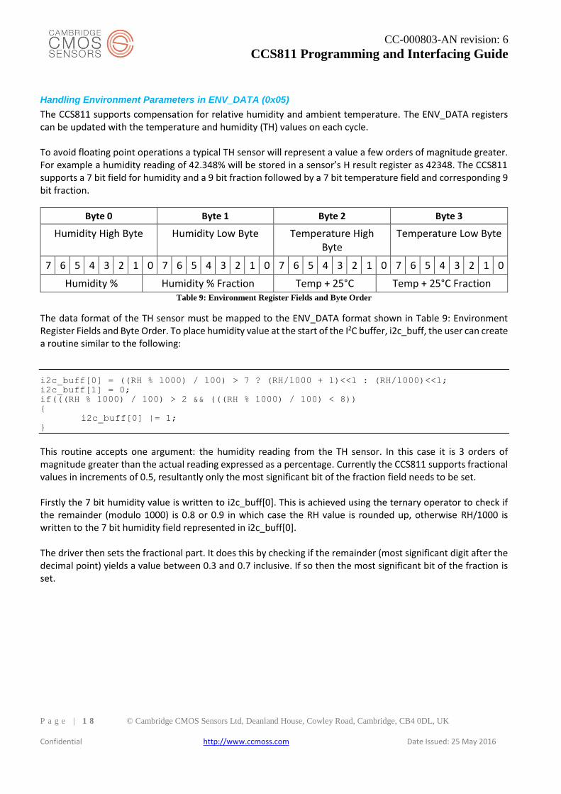
The CCS811 supports compensation for relative humidity and ambient temperature. The ENV_DATA registers can be updated with the temperature and humidity (TH) values on each cycle. To avoid floating point operations a typical TH sensor will represent a value a few orders of magnitude greater. For example a humidity reading of 42.348% will be stored in a sensor’s H result register as 42348. The CCS811 supports a 7 bit field for humidity and a 9 bit fraction followed by a 7 bit temperature field and corresponding 9 bit fraction.
Byte 0 Byte 1 Byte 2 Byte 3
Humidity High Byte Humidity Low Byte Temperature High Byte
Temperature Low Byte
7 6 5 4 3 2 1 0 7 6 5 4 3 2 1 0 7 6 5 4 3 2 1 0 7 6 5 4 3 2 1 0
Humidity % Humidity % Fraction Temp + 25°C Temp + 25°C Fraction Table 9: Environment Register Fields and Byte Order
The data format of the TH sensor must be mapped to the ENV_DATA format shown in Table 9: Environment Register Fields and Byte Order. To place humidity value at the start of the I2C buffer, i2c_buff, the user can create a routine similar to the following:
i2c_buff[0] = ((RH % 1000) / 100) > 7 ? (RH/1000 + 1)<<1 : (RH/1000)<<1;
i2c_buff[1] = 0;
if(((RH % 1000) / 100) > 2 && (((RH % 1000) / 100) < 8))
{
i2c_buff[0] |= 1;
}
This routine accepts one argument: the humidity reading from the TH sensor. In this case it is 3 orders of magnitude greater than the actual reading expressed as a percentage. Currently the CCS811 supports fractional values in increments of 0.5, resultantly only the most significant bit of the fraction field needs to be set. Firstly the 7 bit humidity value is written to i2c_buff[0]. This is achieved using the ternary operator to check if the remainder (modulo 1000) is 0.8 or 0.9 in which case the RH value is rounded up, otherwise RH/1000 is written to the 7 bit humidity field represented in i2c_buff[0]. The driver then sets the fractional part. It does this by checking if the remainder (most significant digit after the decimal point) yields a value between 0.3 and 0.7 inclusive. If so then the most significant bit of the fraction is set.
CC-000803-AN revision: 6
CCS811 Programming and Interfacing Guide
P a g e | 1 9 © Cambridge CMOS Sensors Ltd, Deanland House, Cowley Road, Cambridge, CB4 0DL, UK
Confidential http://www.ccmoss.com Date Issued: 25 May 2016
In a similar manner a routine for placing the temperature value into i2c_buff can be generated as follows.
TEMP += 25000;
i2c_buff[2] = ((TEMP % 1000) / 100) > 7 ? (TEMP/1000 + 1)<<1 : (TEMP/1000)<<1;
i2c_buff[3] = 0;
if(((TEMP % 1000) / 100) > 2 && (((TEMP % 1000) / 100) < 8))
{
i2c_buff[2] |= 1;
}
The bolded code takes care of the data sheet requirement that current temp value plus 25 is written to the ENV_DATA’s temperature register. To program ENV_DATA The user code would therefore look similar to the following:
u32 TEMP, RH;
read_temp_hum_sensor(TEMP, RH);
ccs811_temp_hum_convert(TEMP, RH);
i2c_write(CCS_811_ADDRESS, ENV_DATA, i2c_buff, 4);
The ccs811_temp_hum_convert combines the 2 examples shown above to render the values extracted from the RH into the format required by the CCS811’s ENV_DATA registers (stored in i2c_buff). After this the user can program the ENV_DATA to the sensor in the normal manner using the i2c_write routine. If the application supports temperature or humidity compensation, but not both, the data sheet’s default value must written to the register corresponding to the unsupported environment parameter. The user must not write zero to the unsupported temperature or humidity field of the ENV_DATA register.
CC-000803-AN revision: 6
CCS811 Programming and Interfacing Guide
P a g e | 2 0 © Cambridge CMOS Sensors Ltd, Deanland House, Cowley Road, Cambridge, CB4 0DL, UK
Confidential http://www.ccmoss.com Date Issued: 25 May 2016
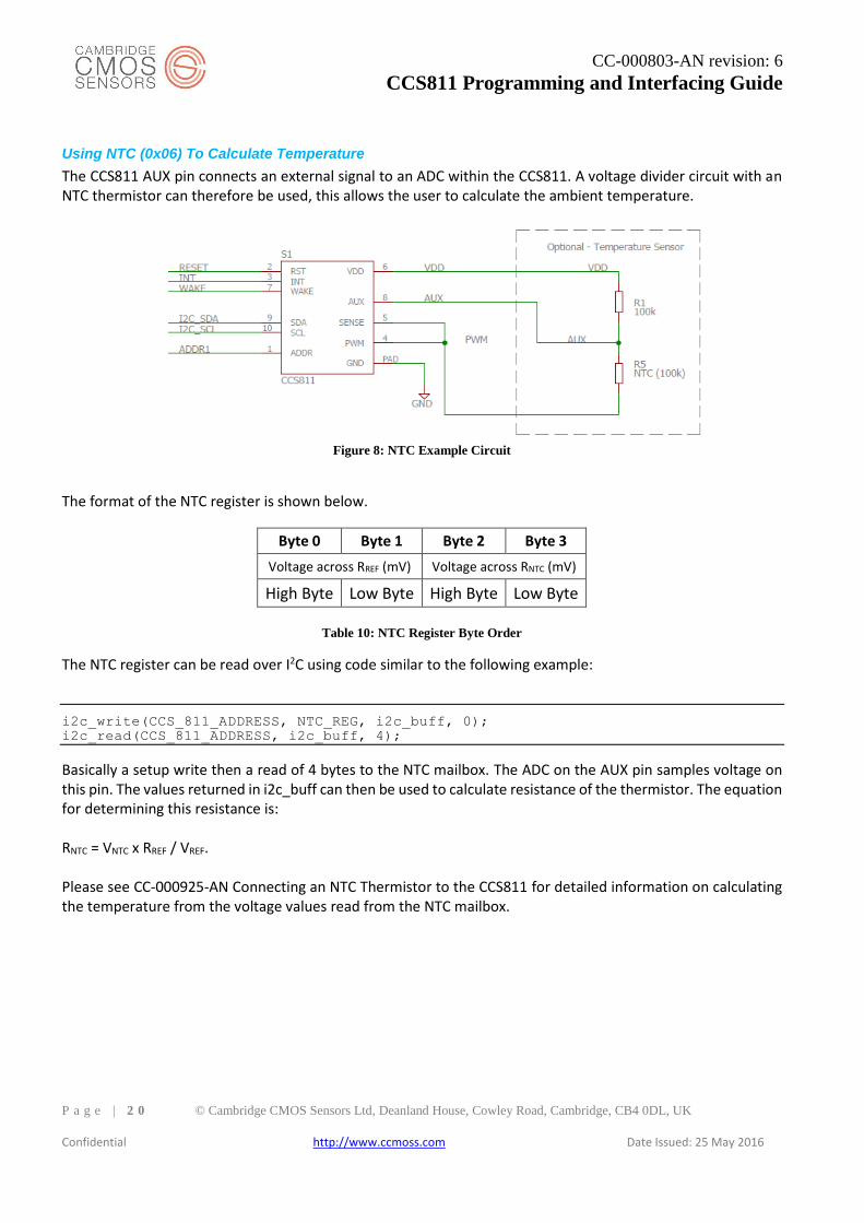
Using NTC (0x06) To Calculate Temperature
The CCS811 AUX pin connects an external signal to an ADC within the CCS811. A voltage divider circuit with an NTC thermistor can therefore be used, this allows the user to calculate the ambient temperature.
Figure 8: NTC Example Circuit
The format of the NTC register is shown below.
Byte 0 Byte 1 Byte 2 Byte 3
Voltage across RREF (mV) Voltage across RNTC (mV)
High Byte Low Byte High Byte Low Byte
Table 10: NTC Register Byte Order
The NTC register can be read over I2C using code similar to the following example:
i2c_write(CCS_811_ADDRESS, NTC_REG, i2c_buff, 0);
i2c_read(CCS_811_ADDRESS, i2c_buff, 4);
Basically a setup write then a read of 4 bytes to the NTC mailbox. The ADC on the AUX pin samples voltage on this pin. The values returned in i2c_buff can then be used to calculate resistance of the thermistor. The equation for determining this resistance is: RNTC = VNTC x RREF / VREF. Please see CC-000925-AN Connecting an NTC Thermistor to the CCS811 for detailed information on calculating the temperature from the voltage values read from the NTC mailbox.
CC-000803-AN revision: 6
CCS811 Programming and Interfacing Guide
P a g e | 2 1 © Cambridge CMOS Sensors Ltd, Deanland House, Cowley Road, Cambridge, CB4 0DL, UK
Confidential http://www.ccmoss.com Date Issued: 25 May 2016
Handling the BASELINE register (0x11)
The BASELINE register can be used to ensure that the CCS811 operates in a stable and consistent manner after each power on, regardless of the ambient air quality (e.g. if the sensor is started in ‘dirty’ air). To use this mechanism the application software must read and store the BASELINE register when the ambient air is fresh. The BASELINE register value is meaningless to the host application as it is encoded to a format used by the CCS811. The application software need only read this value and store it locally. It is not mandatory to write to this register, the CCS811 will configure and manage its baseline autonomously. The BASELINE register can be read and its value stored as follows:
u8 baseline_reg[2]; // storage for baseline value in clean air
if(air_is_clean(eCO2, CO2)){
i2c_write(CCS_811_ADDRESS, BASELINE, baseline_reg, 0);
i2c_read(CCS_811_ADDRESS, baseline_reg, 4);
}
The applications determines if the air is fresh. If so it performs a setup write to BASELINE then a read of 2 bytes into an array storage parameter baseline_reg. The baseline_reg parameter is therefore available to the user to write back to the BASELINE register:
i2c_write(CCS_811_ADDRESS, BASELINE, baseline_reg, 2);
This writes the 2 bytes stored in baseline_reg to the BASELINE register on the CCS811, setting the CCS811 baseline to its resistance in clean air. It will typically be written after each power on of the CCS811 after the sensor has stabilized. The BASELINE register can only be written when the CCS811 MEAS_MODE[DRIVE_MODE] is not in the idle state. Due to the long term drift of MOX sensors it is recommended that new clean baselines are stored periodically.
CC-000803-AN revision: 6
CCS811 Programming and Interfacing Guide
P a g e | 2 2 © Cambridge CMOS Sensors Ltd, Deanland House, Cowley Road, Cambridge, CB4 0DL, UK
Confidential http://www.ccmoss.com Date Issued: 25 May 2016
Host Processor Endianness
The endianness of the host processor needs to be known in order to process the eCO2 and TVOC values. Taking the previous example above where i2c_buff is loaded with:
i2c_buff[0] = 0x01
i2c_buff[1] = 0x90
i2c_buff[2] = 0x00
i2c_buff[3] = 0x32
Where eCO2 = 0x0190 and TVOC = 0x32. If we assume that the i2c_buff is located at physical address 0x1000 in the host CPU’s memory map, the memory will be written as shown in Figure 9 by the i2c_read function:
Address 0x1000 0x1001 0x1002 0x1003
Data 0x01 0x90 0x00 0x32
Figure 9: Big Endian Storage of I2C Read Data
A CPU with a little endian memory storage policy for data will not be able to access these values directly. A conversion/accessor function must be used that handles the endianness conversion from big endian to little endian. Some operating systems, e.g. Linux, support these endianness aware accessor functions and will apply the appropriate endianness formatting based on the size of the scalar being accessed.
If no such functions are available in an environment, the software driver must perform this by either using c code or inline assembly directives that utilize endianness accelerated swap opcodes. For example to ensure that a CPU register is given the correct value of the eCO2 reading the following can be used:
eco2_data = ((uint16_t)i2c_buf[0] << 8) | ((uint32_t)i2c_buf[1] << 0));
If the user’s CPU supports endianness swapping assembly instructions then it is more efficient to use these.
CC-000803-AN revision: 6
CCS811 Programming and Interfacing Guide
P a g e | 2 3 © Cambridge CMOS Sensors Ltd, Deanland House, Cowley Road, Cambridge, CB4 0DL, UK
Confidential http://www.ccmoss.com Date Issued: 25 May 2016
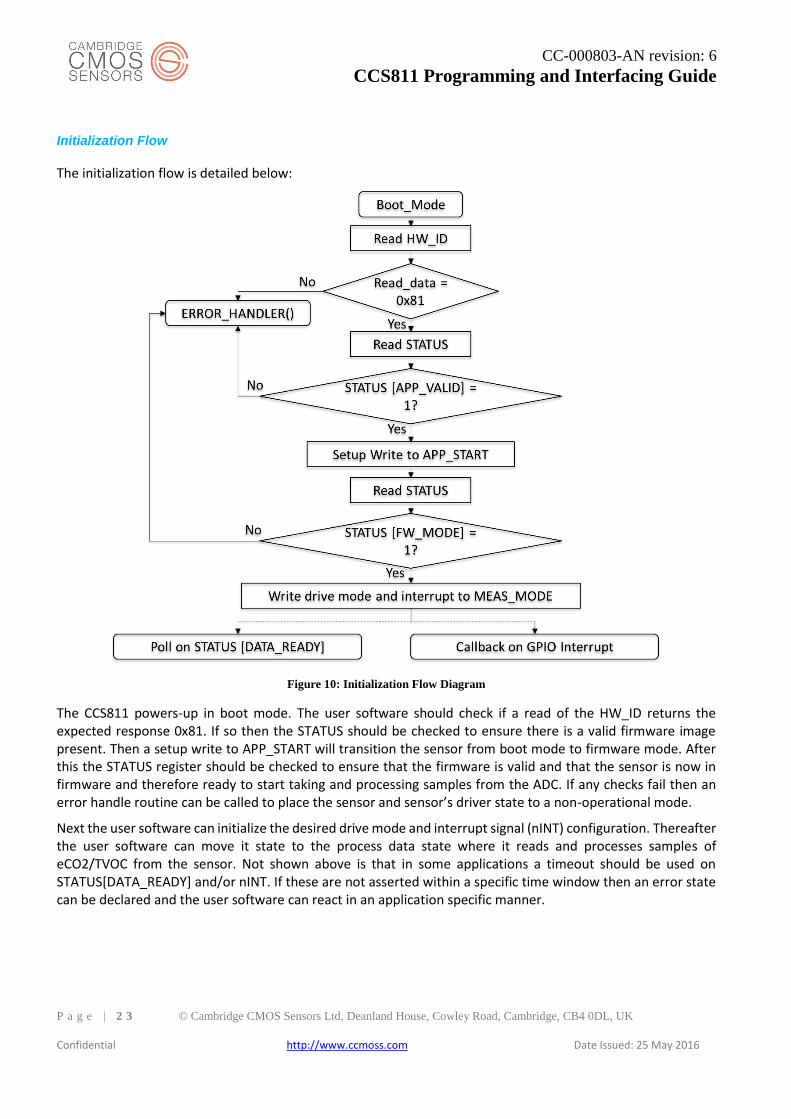
Initialization Flow
The initialization flow is detailed below:
Figure 10: Initialization Flow Diagram
The CCS811 powers-up in boot mode. The user software should check if a read of the HW_ID returns the expected response 0x81. If so then the STATUS should be checked to ensure there is a valid firmware image present. Then a setup write to APP_START will transition the sensor from boot mode to firmware mode. After this the STATUS register should be checked to ensure that the firmware is valid and that the sensor is now in firmware and therefore ready to start taking and processing samples from the ADC. If any checks fail then an error handle routine can be called to place the sensor and sensor’s driver state to a non-operational mode.
Next the user software can initialize the desired drive mode and interrupt signal (nINT) configuration. Thereafter the user software can move it state to the process data state where it reads and processes samples of eCO2/TVOC from the sensor. Not shown above is that in some applications a timeout should be used on STATUS[DATA_READY] and/or nINT. If these are not asserted within a specific time window then an error state can be declared and the user software can react in an application specific manner.
CC-000803-AN revision: 6
CCS811 Programming and Interfacing Guide
P a g e | 2 4 © Cambridge CMOS Sensors Ltd, Deanland House, Cowley Road, Cambridge, CB4 0DL, UK
Confidential http://www.ccmoss.com Date Issued: 25 May 2016
Document Reference Description
CC-000619-DS Datasheet for CCS811
CC-000774-AN Assembly guidelines for CCS811
CC-000783-AN Mechanical considerations for CCS811
CC-000922-AN Performing an Application code binary file download
CC-000925-AN Connecting an NTC Thermistor to the CCS811
The contents of this document are subject to change without notice. CCS products are not designed, authorized or warranted to be suitable for use in medical, military, aircraft, space or life
support equipment, nor in applications where failure or malfunction of an CCS product can reasonably be expected to result in personal injury, death or severe property or environmental
damage. CCS accepts no liability for inclusion and/or use of CCS products in such equipment or applications and therefore such inclusion and/or use, is at the customer’s own risk. As any
devices operated at high temperature have inherently a certain rate of failure, it is therefore necessary to protect against injury, damage or loss from such failures by incorporating appropriate
safety measures
Abbreviation Description
ADC Analogue To Digital Converter
CCS Cambridge CMOS Sensors
CMOS Complementary Metal Oxide Semiconductor
eCO2 Equivalent Carbon Dioxide
I2C Inter-Integrated Circuit
MOX Metal Oxide
NTC Negative Thermal Coefficient
PPM Parts per Million
PPB Parts per Billion
TH Temperature Humidity
TVOC Total Volatile Organic Compound
Abbreviations
References