Embed Size (px)
Citation preview

MEASUREMENT OF MUON LIFE TIME USING COSMIC RAY MUONS STOPPED IN A PLASTIC SCINTILLATOR DETECTOR Lakshmi S Mohan1.INTRODUCTION
Leptons are a class of fundamental building blocks of matter as proposed by the Standard Model of Particle Physics. There are three generations of leptons with the electron and electron neutrino(1st
generation), muon and muon neutrino (2nd generation) and tau and tau neutrino (3rd generation). These are all fermions with spin ½, and all particles other than neutrinos carry one unit of negative charge, where as the corresponding antiparticles carry one unit of positive charge. Muon has a mass of 105.66MeV/c2 and interact only via weak and electromagnetic interactions. Due to this large mass, it is unstable.While passing through matter it can undergo either of the following interactions: capture of muon by nuclei or spontaneous decay as follows, which is a weak decay:
(1)
The later decay is made use of in doing this experiment, since a plastic scintillator (hydrocarbon) and since the muon capturing probability is small for low Z materials. Muon decay times are distributed as follows: N(t) =N(0)exp(t/ ) (2),τwhere, N (0) = initial population of muons,
N(t) = remaining muons at time t,
= the muon life time.τ
This expression is the same as for the general radioactive decays of nuclei and decays of all unstable elementary particles. Muon life time ahs been measured accurately as, = 2.19703 μs.τ
2.COSMIC RAY MUONS
Secondary cosmic rays are used as the source of muons in this experiment. The total secondary flux at the ground level, consists of 75% muons (+ve and ve ) and 25% electrons (e+ and e). Muon flux at sea level is 1cm2min1. Cosmic rays are highenergy particles that fall on the earth from the space. Primary cosmic rays consist of protons(by far the highest proportion), electrons,positrons,neutrinos,and gamma ray photons of very high energies ranging from 108 eV to 1020 eV. On entering the earth's atmosphere, they collide with oxygen and nitrogen nuclei producing secondary cosmic rays, consisting mainly of elementary particles and gammaray photons. A single high energy particle can produce a large shower of secondary particles. The reactions leading to the production of cosmic ray muons are as follows: p+p → p+p+π++π-
π+ → μ++ νμ ; π- → μ-+ ῡμ (weak interaction) (3)
π0 → 2γ (electromagnetic interaction)The spontaneous decay of muon is as follows: μ- → e- +ῡe+ νμ ; μ+ → e+ +ῡμ+ νe (4)
Muon decay time has been calculated accurately as =2.19704 τ μs. Lets say that muon life time is approximately 2.2 μs. This is the value as measured in a reference frame at rest wrt the muon. Using Newtonian mechanics, if the muons travel with velocity ~ c, then they should travel approximately 660m after their creation and should not be detected at the ground level. Only relativistic time dialation can explain the detection of muons at the ground level. By the Lorentz transformation equation, t=t' /1−v2
/c2 = t' (5)γ
t=time measured in the lab systemt'=time measured in the rest frame of the system v=velocity of the systemc=speed of lightFor v~0.99c, =7.08, =2.2 μs, = 15.58 μs is the life time of muons, relative to an observer onγ τ γτ earth. So the average distance travelled by muons as measured by an observer on earth : d = v = 15.58 X 10γτ 6 X 0.99 X 3 X 108 m = 4.627km.
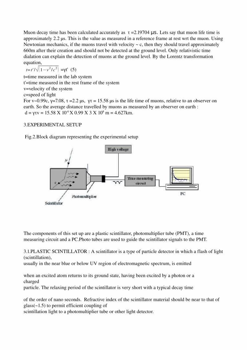
3.EXPERIMENTAL SETUP
Fig.2.Block diagram representing the experimental setup
The components of this set up are a plastic scintillator, photomultiplier tube (PMT), a time measuring circuit and a PC.Photo tubes are used to guide the scintillator signals to the PMT.
3.1.PLASTIC SCINTILLATOR : A scintillator is a type of particle detector in which a flash of light (scintillation), usually in the near blue or below UV region of electromagnetic spectrum, is emitted
when an excited atom returns to its ground state, having been excited by a photon or a chargedparticle. The relaxing period of the scintillator is very short with a typical decay time
of the order of nano seconds. Refractive index of the scintillator material should be near to that of glass(~1.5) to permit efficient coupling of scintillation light to a photomultiplier tube or other light detector.

A plastic scintillator of refractive index 1.58 and dimensions (24 cm X 24 cm X 14.5 cm) , (wrapped first by white tyrek paper to avoid the scintillation light from escaping out, and then by black tedler paper to avoid external light form entering into the detector) is the muon detector used here.
3.2.PHOTOMULTIPLIER TUBE (PMT):The light output of a scintillator is converted into electrical signals and amplified using a photomultiplier tube (PMT).A typical photomultiplier tube consists of a photoemissive cathode (photocathode) followed by focusing electrodes , an electron multiplier (with dynodes) and an electron collector (anode) in a vacuum tube.A PMT is shown in Fig.3.
Fig.3.Structure of a photo multiplier tube.
When light enters the photocathode, the photocathode emits photoelectrons into the vacuum. The number of electrons produced is determined by the quantum efficiency of the photocathode and the number of electrons thus produced is very small. The signal produced by the photo cathode is then focused on dynodes, where secondary emission of electrons proportional to the incident electron energy takes place. The final charges are accumulated and collected at the anode which gives rise to a sharp and strong electrical output. Because of secondary emission multiplication, photomultiplier tubes provide extremely high sensitivity and exceptionally low noise.
The overall spectral response, i.e., the sensitivity of the photocathode is expressed in
terms of quantum efficiency, Q.E.,
Q.E. = (no:of photoelectrons emitted) / (no:of incident photons on the photocathode) (6) For ideal photocathode, Q.E. = 100%, but practically it is 20 – 30%.It is a strong function of the wavelength of the incident light and the photocathode material.
The efficiency of a dynode is determined by the overall multiplication factor ( ),δ
= (no:of emitted secondary electrons) / (no:of incident primary electrons)δ (7)

A 2 inch diameter PMT, with a 21 pin base (9807B, manufactured by Electron Tubes Ltd) , operated at a high voltage of about 1.7 kV by means of high voltage dc to dc converter (E20HVDCDC) was used for this experiment.The rise time of the pulse obtained is a few nanoseconds.
3.3.TIME MEASUREMENT CIRCUIT: A stopped muon decaying inside a scintillator gives rise to two signals; one due to itself and the other due to the electron into which it decays. The time measurement circuit is used to determine the delay between the two signals and then it is passed to a PC.PMT pulse: When the muon passes through the detector, it produces a light signal, which is fed to a PMT, to produce a negative analog pulse. The decay electron also gives a similar pulse, but of smaller height. The two pulses are shown in Fig.4.
Fig.4. PMT pulses. Note the deeper pulse for muon.
The time difference between the entering of a muon into the detector and its decay into the subsequent products should be measured. For this a 'clock' is needed. The electronic circuit designed for this purpose is shown in Fig.5.

Fig.5. Time measurement circuit (top one). The 2 circuits at the bottom of the figure are the voltage regulators for providing voltages to IC’s (+5V and 5V) and PMT base (rated 1.65 kV)
The main components of this circuit are the following: a) Comparator b) Flipflops c) Counters d) Oscillator e) Latches f) a buffer IC and g) a standard Parallel Port interfacing with the computer where the data is recorded. The names and uses of the different ICs used in this circuit are listed in the following table. Table.1.ICs (A description of these ICs is given in the appendix.) IC name Description
LM360 (8 PINS) COMPARATOR
74LS74 (14 PINS) DFLIP FLOP
74LS161 (16 PINS) COUNTER
74LS541 (20 PINS) BUFFER
74LS11 (14 PINS) AND GATE
74LS04 (14 PINS) NOT GATE
7805 (3PINS) POSITIVE VOLTAGE REGULATOR
7905 (3 PINS) NEGATIVE VOLTAGE REGULATOR
LM317 POSITIVE VOLTAGE REGULATOR
DB103 (4 PINS) BRIDGE RECTIFIER
A CRYSTAL OSCILLATOR (4 PINS) of frequency 10 MHz is used to generate the clock for both

LSB and USB counters, thus giving the resolution of 0.1μs.The working of this circuit is described below: The small light pulse produced when a muon stops in the sintillator is detected and ampified by the PMT, the output of which is fed to a comparator. The comparator acts as a noise filter, which will allow only sigals with amplitudes greater than a certain threshold value to pass through. Once there is a signal at the comparator output, it starts a counter, which counts at a rate of 10MHz, giving a resolution of 0.1μs. If a second pulse from a decaying muon arrives soon after the first, the counter is stoped and the PC is signalled that the data is to be read. The PC, after reading the data, resets the circuit ready for more decays. If there's is no second pulse following the first pulse after a certain period, the circuit resets itself and waits for the second pulse to come.
The LM360 high speed comparator is the first stage of the electronic circuit. A potential divider is used to set the threshold for the comparator. The comparator filters out noise by allowing only those
signals which have a voltage higher than the reference voltage, of 42mV, set at the noninverting terminal of the IC,to generate a high logic pulse. The output of the comparator is a positive high (the negative input signal is fed to the inverting terminal) digital pulse (TTL) of 5 Volts. This pulse acts as the clock of the first DF/F. Two flipflops are used in this circuit. In the cleared state, the Q o/p is low and Q’ o/p is high. Q’ o/p of the 1st F/F is connected to its Di/p. when the clock comes, Q goes high and Q’ goes low. The positive high o/p of the LM360 comparator acts as the clock for the 1st F/F. When the clock is present, the Q o/p of the 1st F/F goes high, goes to the ENT of the 1st 4bit synchronous counter and starts counting at 10MHz. The Q’ o/p goes low and is fed to the clock of the 2nd F/F. Since the clock is low, Q o/p of 2nd F/F is low and its Q’ o/p is high.
There are two cases. Case 1: Muon decays into an electron
When a muon decays into an electron, a 2nd pulse comes from the PMT and passes through the comparator soon after the first. Now, the 1st F/F’s Q o/p goes low and stops the counter. Meanwhile the Q’ o/p, which is the clock of the 2nd F/F, goes high, making the Q o/p of the 2nd F/F high and its Q’ o/p low. This low Q’ o/p clears the 1st F/F as well as the counter. The low Q’ is read as the time when the data from the buffer (IC74LS541) is to be read by the interfacing program. Q’ after buffering is sent to the BUSY pin of the PC parallel port. On receiving the BUSY signal, the DATA_STROBE is pulled low to enable the data buffer, which passes the count from the counter to the PC, which reads the data. After reading data, the DATA_STROBE line goes high and the RESET line is pulled low for a few microseconds. This clears the F/F back to the waiting state and the counter is ready for the next PMT signal.
Case 2: Muon doesn’t decay into an electron
The counter will count upto 255, ie. if a second pulse is not received within 25.5μs, the RCO (Ripple Carry Output) goes high. This is inverted to clear the counter and the F/Fs, to wait for the next PMT pulse.
DATA ANALYSIS Data analysis requires fitting of the data with appropriate functions. Measured quantity is the

time lag between the start event and stop event. For time distribution, tha data is sampled, events binned and then fitted. A correction for background events is needed, since there are background sources like other radioactive sources, light leakage through the scintillator or a muon decaying before the decay of the previous one. The background events which are produced due to start from
one muon and stop from another one will be very small as the flux reaching down at sea level is very small when compared to the 25.5μsecs window used for counting. The background for the data is assumed to be constant over a period of time. Then, the function N(t) =N0 exp(t/ τ) + b (8) is fitted using ROOT. The fitting parameters obtained are:
Fig 6: Log of event number vs time. Straight line gives the background.
NO. NAME VALUE ERROR SIZE DERIVATIVE 1 p0 1.17507e+03 1.17805e+01 1.63446e03 1.03881e07 2 p1 2.14951e+01 1.81382e01 2.34723e05 1.04836e05 3 p2 1.88115e+01 3.71917e01 1.20655e05 4.29021e06 b = 18.8115The fitted parameters are obtained as: N(0) = 1175.07 ± 11.78

τ = (21.49 ± 0.18) X 100ns ~ (21.5 ± 0.2) x 100ns b = 18.81 ± 0.37
So, the mean muon life time is determined approximately as, (2.15 ± 0.02)μs.
FERMI COUPLING CONSTANT The universal constants for a process provides a tool to validate experimental results. The muon decay is an electroweak process and the coupling constant is the Fermi Coupling constant (G). In the theory of muon decay the expression for average life time of muon is expressed as τ=(192π3) / (G2mμ
5) (9)Substituting the value of obtained from this experiment, in this equation,the value of Fermiτ coupling constant is obtained as: GF = 1.1753 X 10⁵(GeV)2
Here, the conversion relation 1GeV1 = 6.58 X 1025s, has been used.

APPENDIX I : ELECTRONIC COMPONENTS
LM360 : It is an 8pin configuration IC with a very high speed differential input, complementary TTL output voltage comparator which has been optimized for greater speed, input impedance and fanout, and lower input offset voltage. Typically delay varies only 3 ns for overdrive variations of 5 mV to 400 mV.
The connection diagram is shown in metal can package and dualin line package.
Fig I: Metal Can Package Fig II: DualInLine Package
Features of LM360:
• Tight delay matching on both outputs• Guaranteed high speed: 20 ns max• Complementary TTL outputs• High input impedance• Low speed variation with overdrive variation• Fanout of 4• Low input offset voltage• Series 74 TTL compatible• Positive Supply Voltage : +8V• Negative Supply Voltage: −8V• Peak Output Current 20 mA• Differential Input Voltage ±5V• Input Voltage V+ ≥VIN≥ V−• Operating Temperature Range 0°C to +70°C• Storage temperature range 65°C to +150°C
74LS74 : A dual edge triggered flipflop that utilizes Schottky TTL circuitry to produce high speed Dtype flip – flops. Each flipflop has individual clear and set inputs,and also complementary Q

and Q' outputs.
Fig III: Logic diagram(Individual FlipFlop)
Fig 1V: Logic symbol
The information at the D i/p is transferred to the Q o/p on the +ve going edge of the clock pulse.Clock trigering occurs at a particular voltage level of the clock pulse and is not directly related to the transition time of the +ve going pulse.When the clock i/p is either at HIGH or LOW level,the D input signal has no effect.
Fig V: Connection diagram

Fig VI : Truth table
where, X = LOW or HIGH Logic Level H = HIGH Logic Level
L = LOW Logic Level
= Positivegoing Transition
Q0 = The output logic level of Q before the indicated i/p conditions were established.
Note: This configuration is unstable, i.e. it will not persist when either the preset and/or clear inputs
return to their inactive (HIGH) level.
74LS161: Ahigh speed 4bit synchronous counter with 16 pin configuration.
Fig VII: 74LS161 Connection diagram

The carry output is decoded by means of a NOR gate, thus preventing spikes during the normal
counting mode of operation. Synchronous operation is provided by having all flipflops clocked
simultaneously, so that the outputs change coincidently with each other, when so instructed by the countenable inputs and internal gating.
A buffered clock input triggers the four flipflops on the rising (positivegoing) edge of the clock inputwaveform. These counters are fully programmable, i.e. the outputs may be preset to either level. As presetting is synchronous,setting up a low level at the load input disables the counter and causes the outputsto agree with the setup data after the next clock pulse, regardless of the levels of the enable input. The clear function for the DM74LS161A is asynchronous. A low level at the clear input sets all four of the flipflop outputs LOW, regardless of the levels of clock,load, or enable inputs.
The carry lookahead circuitry provides cascading for counters for nbit synchronous applications
without additional gating. Instrumental in accomplishing this function are two countenable inputs and a ripple carry output. Both countenable inputs (P and T) must be HIGH to count,and input T is fed forward to enable the ripple carry output.The ripple carry output thus enabled will produce a highlevel output pulse with a duration approximately equal to the highlevel portion of the QA output. This highlevel overflow ripple carry pulse can be used to enable successive cascaded stages. HIGHtoLOW level transitions at the enable P or T inputs may occur, regardless of the logic level of the clock.
Table I: Guaranteed Operating Ranges
Parameter Symbol Min Type Max Unit
Supply Voltage Vcc 4.75 5 5.25 V
Operating Ambient
0 2.5 70 0C

Temperature range
TA
Output current
High
IOH 0.4 mA
Output current
Low
IOL 8 mA
74LS541: An octal buffer with 20 pin configuration.It takes 4 bit output from each counter and
gives 8 bit output to the PC.
Fig VIII: Connection diagram
Fig IX: Logic diagram

Fig X: Truth table
74LS11:A 14 pin configuration IC consisting of triple threeinput AND gates.Fig XI: Pin diagram
Fig XII: Truth table
H = HIGH Logic Level

L = LOW Logic Level
X = Either LOW or HIGH Logic Level
Table II: Features Symbol Parameter Min Nom Max Unit
Vcc Supply Voltage 4.75 5 5.25 V
TA Operating Ambient Temperature Range
0 70 0C
IOH Output current High
0.4 mA
IOL Output currentLow
8 mA
VIH Input VoltageHigh
2 V
VIL Input VoltageLow
0.8 V
VOH Output Voltage High
2.7 V
VOL Output VoltageLow
0.5 V
IIH Input High Current
0.1 mA
IIL Input Low Current
0.4 mA
74LS04: A triple 3input AND gate with 14 pins.
Fig XIII: Connection diagram

7805 : It is a three terminal 1A positive voltage regulator which employs internal current limiting, thermal shut down and safe operating area protection,making it essentially indestructible. If adequate heat sinking is provided, they can deliver over 1A output current.
Table III:Absolute Maximum Ratings
Parameter Symbol Value Unit
Input voltage (for V0
=5V to 18V) VI 35 V
Input voltage (for V0
=24V) VI 40 V
Thermal Resistance Junction Cases (T O 220)
RθJC 5 0C/W
Thermal Resistance JunctionAir (TO220)
RθJC 65 0C/W
Operating Temperature Range (KA78XX)
TOPR 0 ~ +125 0C
Storage Temperature Range
TSTG 65 ~ +150 0C
7905: It is a three terminal negative voltage regulator with thermal overload protection and short circuit protection.
Table IV: Absolute maximum ratings
Parameter Symbol Value Unit
Input voltage (for V0
=5V to 18V) VI 35 V
Input voltage (for V0
=20V,24V) VI 40 V
Output Current IOUT Internally limited
Power Dissipation PO Internally limited W
Operating Temperature TOPR 0 ~ 150 0C

Range (KA78XX)
Storage Temperature Range
TSTG 65 ~ +150 0C
LM317 : An adjustible three terminal positive voltage regulator designed to supply more than 1.5A of load current with an output voltage adjustible over 1.2 to 37V. It employs internal current limiting, thermal shutdown and safe area compensation.
Table V: Absolute maximum ratingsParameter Symbol Value Unit
Input output Voltage: Differential
Vi Vo 40 V
Lead temperature Tlead 230 0C
Power dissipation PD Internally limited W
Operating junction temperature range
TJ
0 125 0C
Temperature coefficient of Output voltage
ΔV0/ΔT ±0.02 %/ 0C
Storage Temperature Range
TSTG 65 ~ +150 0C