Embed Size (px)
Citation preview

Freescale SemiconductorData Sheet: Advance Information
Document Number: MC9S08QE128Rev. 4, 11/2007
MC9S08QE128MC9S08QE128 SeriesCovers: MC9S08QE128, MC9S08QE96, MC9S08QE64,MCF51QE32
• 8-Bit HCS08 Central Processor Unit (CPU)– Up to 50.33-MHz HCS08 CPU from 3.6V to 2.1V, and
20-MHz CPU at 2.1V to 1.8V across temperature range – HC08 instruction set with added BGND instruction– Support for up to 32 interrupt/reset sources
• On-Chip Memory– Flash read/program/erase over full operating voltage
and temperature– Random-access memory (RAM)– Security circuitry to prevent unauthorized access to
RAM and flash contents• Power-Saving Modes
– Two low power stop modes; reduced power wait mode– Peripheral clock enable register can disable clocks to
unused modules, reducing currents; allows clocks to remain enabled to specific peripherals in stop3 mode
– Very low power external oscillator can be used in stop3 mode to provide accurate clock to active peripherals
– Very low power real time counter for use in run, wait, and stop modes with internal and external clock sources
– 6 μs typical wake up time from stop modes• Clock Source Options
– Oscillator (XOSC) — Loop-control Pierce oscillator; Crystal or ceramic resonator range of 31.25 kHz to 38.4 kHz or 1 MHz to 16 MHz
– Internal Clock Source (ICS) — FLL controlled by internal or external reference; precision trimming of internal reference allows 0.2% resolution and 2% deviation; supports CPU freq. from 2 to 50.33 MHz
• System Protection– Watchdog computer operating properly (COP) reset
with option to run from dedicated 1-kHz internal clock source or bus clock
– Low-voltage detection with reset or interrupt; selectable trip points
– Illegal opcode detection with reset– Flash block protection
• Development Support– Single-wire background debug interface– Breakpoint capability to allow single breakpoint setting
during in-circuit debugging (plus two more breakpoints)– On-chip in-circuit emulator (ICE) debug module
containing two comparators and nine trigger modes. Eight deep FIFO for storing change-of-flow addresses
© Freescale Semiconductor, Inc., 2007. All rights reserved.
This document contains information on a new product. Specificaare subject to change without notice.
and event-only data. Debug module supports both tag and force breakpoints.
• ADC — 24-channel, 12-bit resolution; 2.5 μs conversion time; automatic compare function; 1.7 mV/°C temperature sensor; internal bandgap reference channel; operation in stop3; fully functional from 3.6V to 1.8V
• ACMPx — Two analog comparators with selectable interrupt on rising, falling, or either edge of comparator output; compare option to fixed internal bandgap reference voltage; outputs can be optionally routed to TPM module; operation in stop3
• SCIx — Two SCIs with full duplex non-return to zero (NRZ); LIN master extended break generation; LIN slave extended break detection; wake up on active edge
• SPIx— Two serial peripheral interfaces with Full-duplex or single-wire bidirectional; Double-buffered transmit and receive; MSB-first or LSB-first shifting
• IICx — Two IICs with; Up to 100 kbps with maximum bus loading; Multi-master operation; Programmable slave address; Interrupt driven byte-by-byte data transfer; supports broadcast mode and 10 bit addressing
• TPMx — One 6-channel and two 3-channel; Selectable input capture, output compare, or buffered edge- or center-aligned PWMs on each channel
• RTC — 8-bit modulus counter with binary or decimal based prescaler; External clock source for precise time base, time-of-day, calendar or task scheduling functions; Free running on-chip low power oscillator (1 kHz) for cyclic wake-up without external components
• Input/Output– 70 GPIOs and 1 input-only and 1 output-only pin– 16 KBI interrupts with selectable polarity– Hysteresis and configurable pull-up device on all input
pins; Configurable slew rate and drive strength on all output pins.
– SET/CLR registers on 16 pins (PTC and PTE)
80-LQFPCase 917A14 mm2
64-LQFPCase 840F10 mm2
48-QFNCase 13147 mm2
32-LQFPCase 873A7 mm2
44-LQFPCase 824D10 mm2
tions and information herein

MC9S08QE128 Series Advance Information Data Sheet, Rev. 4
Freescale Semiconductor2
Table of Contents1 MC9S08QE128 Series Comparison . . . . . . . . . . . . . . . . . . . . .42 Pin Assignments . . . . . . . . . . . . . . . . . . . . . . . . . . . . . . . . . . . .53 Electrical Characteristics . . . . . . . . . . . . . . . . . . . . . . . . . . . .12
3.1 Introduction . . . . . . . . . . . . . . . . . . . . . . . . . . . . . . . . . .123.2 Parameter Classification . . . . . . . . . . . . . . . . . . . . . . . .123.3 Absolute Maximum Ratings . . . . . . . . . . . . . . . . . . . . .123.4 Thermal Characteristics . . . . . . . . . . . . . . . . . . . . . . . .133.5 ESD Protection and Latch-Up Immunity . . . . . . . . . . . .143.6 DC Characteristics . . . . . . . . . . . . . . . . . . . . . . . . . . . .153.7 Supply Current Characteristics . . . . . . . . . . . . . . . . . . .183.8 External Oscillator (XOSC) Characteristics . . . . . . . . .213.9 Internal Clock Source (ICS) Characteristics . . . . . . . . .223.10 AC Characteristics . . . . . . . . . . . . . . . . . . . . . . . . . . . .24
3.10.1 Control Timing . . . . . . . . . . . . . . . . . . . . . . . . . .243.10.2 TPM Module Timing. . . . . . . . . . . . . . . . . . . . . .26
3.10.3 SPI Timing . . . . . . . . . . . . . . . . . . . . . . . . . . . . 273.10.4 Analog Comparator (ACMP) Electricals . . . . . . 303.10.5 ADC Characteristics. . . . . . . . . . . . . . . . . . . . . 303.10.6 Flash Specifications . . . . . . . . . . . . . . . . . . . . . 33
3.11 EMC Performance. . . . . . . . . . . . . . . . . . . . . . . . . . . . 333.11.1 Radiated Emissions . . . . . . . . . . . . . . . . . . . . . 343.11.2 Conducted Transient Susceptibility . . . . . . . . . 34
4 Ordering Information . . . . . . . . . . . . . . . . . . . . . . . . . . . . . . . 354.1 Device Numbering System . . . . . . . . . . . . . . . . . . . . . 36
5 Package Information . . . . . . . . . . . . . . . . . . . . . . . . . . . . . . . 365.1 Mechanical Drawings . . . . . . . . . . . . . . . . . . . . . . . . . 36
6 Product Documentation. . . . . . . . . . . . . . . . . . . . . . . . . . . . . 517 Revision History . . . . . . . . . . . . . . . . . . . . . . . . . . . . . . . . . . 51

Figure 1. MC9S08QE128 Series Block Diagram
TPM2CH2-0
TPM1CH2-0
ANALOG COMPARATOR(ACMP1)
ACMP1O
ACMP1-
ACMP1+
VSS
VDD
IIC MODULE (IIC1)
SERIAL PERIPHERAL INTERFACE MODULE (SPI1)
USER FLASH
USER RAM
128K / 96K / 64K
HCS08 CORE
CPU
BDC
6-CHANNEL TIMER/PWM
MODULE (TPM3)
HCS08 SYSTEM CONTROL
RESETS AND INTERRUPTSMODES OF OPERATIONPOWER MANAGEMENT
VOLTAGE
REGULATOR
COP
IRQ
LVD
OSCILLATOR (XOSC)
RE
SE
T
VREFL
VREFH
8K / 6K / 4K
BK
GD
/MS
INTERFACE (SCI1)SERIAL COMMUNICATIONS
MISO1SS1
SPSCK1
3-CHANNEL TIMER/PWM
MODULE (TPM2)
REAL TIME COUNTER (RTC)
DEBUG MODULE (DBG)
IRQ
PTA3/KBI1P3/SCL1/ADP3
PTA4/ACMP1O/BKGD/MS
PTA5/IRQ/TPM1CLK/RESET
PTA2/KBI1P2/SDA1/ADP2
PTA1/KBI1P1/TPM2CH0/ADP1/ACMP1-
PTA0/KBI1P0/TPM1CH0/ADP0/ACMP1+
PO
RT
A
PTA6/TPM1CH2/ADP8
PTA7/TPM2CH2/ADP9
MOSI1
PTB3/KBI1P7/MOSI1/ADP7
PTB4/TPM2CH1/MISO1
PTB5/TPM1CH1/SS1
PTB2/KBI1P6/SPSCK1/ADP6
PTB1/KBI1P5/TxD1/ADP5
PTB0/KBI1P4/RxD1/ADP4
PO
RT
B
PTB6/SDA1/XTAL
PTB7/SCL1/EXTAL
PTC3/TPM3CH3
PTC4/TPM3CH4/RSTO
PTC5/TPM3CH5/ACMP2O
PTC2/TPM3CH2
PTC1/TPM3CH1
PTC0/TPM3CH0
PO
RT
C
PTC6/RxD2/ACMP2+
PTC7/TxD2/ACMP2-
PTD3/KBI2P3/SS2
PTD4/KBI2P4
PTD5/KBI2P5
PTD2/KBI2P2/MISO2
PTD1/KBI2P1/MOSI2
PTD0/KBI2P0/SPSCK2
PO
RT
D
PTD6/KBI2P6
PTD7/KBI2P7
PTE3/SS1
PTE4
PTE5
PTE2/MISO1
PTE1/MOSI1
TPM2CLK
PO
RT
E
PTE6
PTE0/TPM2CLK/SPSCK1
PTF3/ADP13
PTF4/ADP14
PTF5/ADP15
PTF2/ADP12
PTF1/ADP11
PTF0/ADP10
PO
RT
F
PTF6/ADP16
PTF7/ADP17
PTG1
PTG2/ADP18
PTG3/ADP19
PO
RT
G
PTG4/ADP20
PTG5/ADP21
PTG0
VSS
VDD
VSSA
VDDA
BKP
INT
ANALOG COMPARATOR
(ACMP2)
INTERFACE (SCI2)
SERIAL COMMUNICATIONS
6
TPM3CH5-0
- VREFH/VREFL internally connected to VDDA/VSSA in 48-pin and 32-pin packages- VDD and VSS pins are each internally connected to two pads in 32-pin package
PTG6/ADP22PTG7/ADP23
SOURCE (ICS)INTERNAL CLOCK
PO
RT
JP
OR
T H
PTJ1PTJ2PTJ3PTJ4PTJ5
PTJ0
PTJ6PTJ7
PTH1PTH2PTH3PTH4PTH5
PTH0
PTH6/SCL2PTH7/SDA2
IIC MODULE (IIC2)
ANALOG-TO-DIGITALCONVERTER (ADC)
24-CHANNEL,12-BIT
3-CHANNEL TIMER/PWM
MODULE (TPM1)
SDA2SCL2
SERIAL PERIPHERAL
INTERFACE MODULE (SPI2)
MISO2SS2
SPSCK2
MOSI2
EXTAL
XTAL
10
SDA1SCL1
ACMP2-
ACMP2+
ACMP2O
RxD1
TxD1
RxD2
TxD2
TPM3CLK
3
TPM1CLK
PTE7/TPM3CLK
MC9S08QE128 Series Advance Information Data Sheet, Rev. 4
Freescale Semiconductor 3

MC9S08QE128 Series Comparison
1 MC9S08QE128 Series ComparisonThe following table compares the various device derivatives available within the MC9S08QE128 series.
Table 1. MC9S08QE128 Series Features by MCU and Package
Feature MC9S08QE128 MC9S08QE96 MC9S08QE64
Flash size (bytes) 131072 98304 65536
RAM size (bytes) 8064 6016 4096
Pin quantity 80 64 48 44 80 64 48 44 64 48 44 32
ACMP1 yes
ACMP2 yes
ADC channels 24 22 10 10 24 22 10 10 22 10 10 10
DBG yes
ICS yes
IIC1 yes
IIC2 yes yes no no yes yes no no yes no no no
IRQ yes
KBI 16 16 16 16 16 16 16 16 16 16 16 12
Port I/O1
1 Port I/O count does not include the input only PTA5/IRQ/TPM1CLK/RESET or the output only PTA4/ACMP1O/BKGD/MS.
70 54 38 34 70 54 38 34 54 38 34 26
RTC yes
SCI1 yes
SCI2 yes
SPI1 yes
SPI2 yes
TPM1 channels 3
TPM2 channels 3
TPM3 channels 6
XOSC yes
MC9S08QE128 Series Advance Information Data Sheet, Rev. 4
Freescale Semiconductor4

Pin Assignments
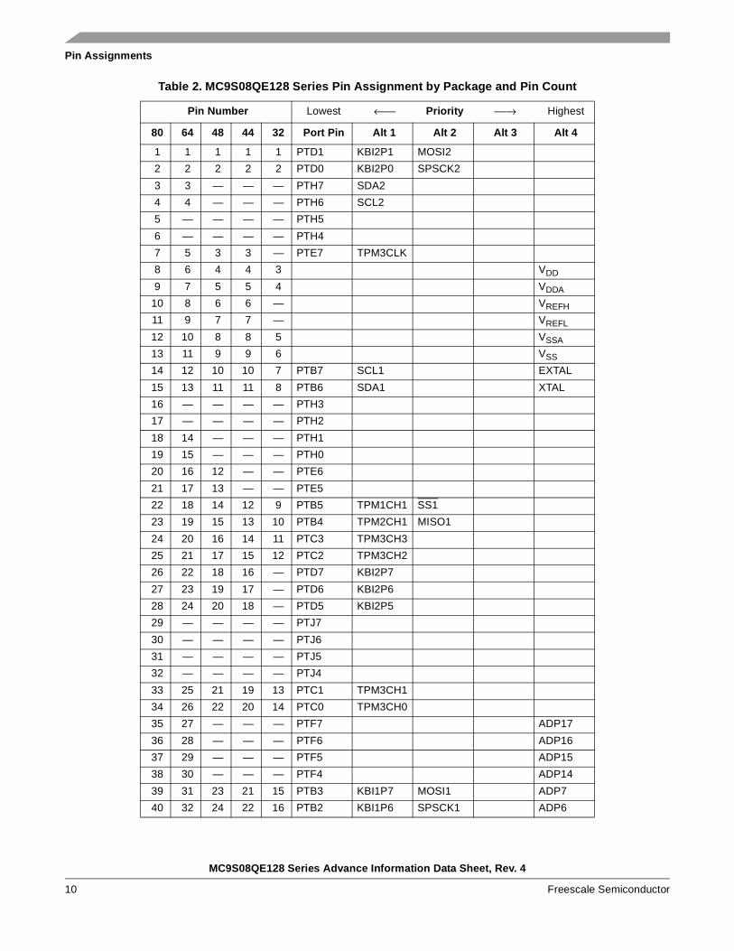
2 Pin AssignmentsThis section describes the pin assignments for the available packages. See Table 2 for pin availability by package pin-count.
Figure 2. Pin Assignments in 80-Pin LQFP
1234567891011121314151617181920
80 79 78 77 76 75 74 73 72 71 70 69 68 67 66 65 64 63 62 61
21 22 23 24 25 26 27 28 29 30 31 32 33 34 35 36 37 38 39 40
6059585756555453525150494847464544434241
VREFH
VSSAD
VDD
VREFL
VDDAD
VSS
PTB7/SCL1/EXTAL
PTH7/SDA2
PTD0/KBI2P0/SPSCK2PTD1/KBI2P1/MOSI2
PTE6
PTB6/SDA1/XTAL
PTH6/SCL2
PTE7/TPM3CLK
PTH1PTH0
PTH3PTH2
PTH5PTH4
PT
C2
/TP
M3C
H2
PT
B4/
TP
M2C
H1/
MIS
O1
PT
B5
/TP
M1C
H1
/SS
1
PT
C3
/TP
M3C
H3
PT
D7/
KB
I2P
7
PT
C0
/TP
M3C
H0
PT
C1
/TP
M3C
H1
PT
D6/
KB
I2P
6
PT
D5/
KB
I2P
5
PT
B3/
KB
I1P
7/M
OS
I1/A
DP
7
PT
B2
/KB
I1P
6/S
PS
CK
1/A
DP
6
PT
E5
PT
F7/
AD
P17
PT
F6/
AD
P16
PT
F5/
AD
P15
PT
F4/
AD
P14
PTD4/KBI2P4
VDD
VSS
PTA7/TPM2CH2/ADP9
PTB1/KBI1P5/TxD1/ADP5PTB0/KBI1P4/RxD1/ADP4
PTA2/KBI1P2/SDA1/ADP2PTA3/KBI1P3/SCL1/ADP3
PTA6/TPM1CH2/ADP8
PTD3/KBI2P3/SS2
PTD2/KBI2P2/MISO2
PTE4
PTF0/ADP10PTF1/ADP11
PTF2/ADP12PTF3/ADP13
PT
E2/
MIS
O1
PT
A5/
IRQ
/TP
M1C
LK/R
ES
ET
PT
A4/
AC
MP
1O
/BK
GD
/MS
PT
A0/
KB
I1P
0/T
PM
1CH
0/A
DP
0/A
CM
P1
+
PT
C7/
TxD
2/A
CM
P2-
PT
C5/
TP
M3
CH
5/A
CM
P2O
PT
C4/
TP
M3
CH
4/R
ST
O
PT
C6/
RxD
2/A
CM
P2+
PT
E0/
TP
M2C
LK/S
PS
CK
1P
TE
1/M
OS
I1
PT
E3/
SS
1
PT
G3/
AD
P1
9
PT
G2/
AD
P1
8P
TG
1P
TG
0
PT
G7/
AD
P23
PT
G6/
AD
P22
PT
G5/
AD
P21
PT
G4/
AD
P20
PTJ
4P
TJ5
PTJ
6P
TJ7
PTJ1PTJ0
PTJ3PTJ2
PT
A1/
KB
I1P
1/T
PM
2CH
0/A
DP
1/A
CM
P1
-
Pins in bold are added from the next smaller package.
MC9S08QE128 Series Advance Information Data Sheet, Rev. 4
Freescale Semiconductor 5

Pin Assignments
Figure 3. Pin Assignments in 64-Pin LQFP Package
12345678910111213141516
17 18 19 20 21 22 23 24 25 26 27 28 29 30 31 32
48474645444342414039383736353433
64 63 62 61 60 59 58 57 56 55 54 53 52 51 50 49
VREFH
VSSAD
VDD
VREFL
VDDAD
VSS
PTB7/SCL1/EXTAL
PTH7/SDA2PTD0/KBI2P0/SPSCK2
PTD1/KBI2P1/MOSI2
PTE6
PTB6/SDA1/XTAL
PT
C2/
TP
M3
CH
2
PT
B4/
TP
M2C
H1/
MIS
O1
PT
B5
/TP
M1C
H1
/SS
1
PT
C3/
TP
M3
CH
3
PT
D7/
KB
I2P
7
PT
C0/
TP
M3
CH
0
PT
C1/
TP
M3
CH
1
PT
D6/
KB
I2P
6
PT
D5/
KB
I2P
5
PT
B3/
KB
I1P
7/M
OS
I1/A
DP
7
PT
B2/
KB
I1P
6/S
PS
CK
1/A
DP
6
PT
E5
PTD4/KBI2P4
VDD
VSS
PTA7/TPM2CH2/ADP9
PTB1/KBI1P5/TxD1/ADP5PTB0/KBI1P4/RxD1/ADP4
PTA2/KBI1P2/SDA11/ADP2PTA3/KBI1P3/SCL1/ADP3
PTA6/TPM1CH2/ADP8
PTD3/KBI2P3/SS2
PTD2/KBI2P2/MISO2
PTE4
PT
E2
/MIS
O1
PT
A5
/IRQ
/TP
M1C
LK/R
ES
ET
PT
A4
/AC
MP
1O/B
KG
D/M
S
PT
A0
/KB
I1P
0/T
PM
1CH
0/A
DP
0/A
CM
P1+
PT
A1
/KB
I1P
1/T
PM
2CH
0/A
DP
1/A
CM
P1-
PT
C7/
TxD
2/A
CM
P2-
PT
C5/
TP
M3C
H5/
AC
MP
2O
PT
C4/
TP
M3C
H4/
RS
TO
PT
C6
/RxD
2/A
CM
P2+
PT
E0
/TP
M2C
LK
/SP
SC
K1
PT
E1
/MO
SI1
PT
E3
/SS
1
PTF0/ADP10PTF1/ADP11
PT
F7/
AD
P17
PT
F6/
AD
P16
PT
F5/
AD
P15
PT
F4/
AD
P14
PTF2/ADP12PTF3/ADP13
PT
G3/
AD
P19
PT
G2/
AD
P18
PT
G1
PT
G0
PTH6/SCL2PTE7/TPM3CLK
PTH1PTH0
Pins in bold are added from the next smaller package.
MC9S08QE128 Series Advance Information Data Sheet, Rev. 4
Freescale Semiconductor6

Pin Assignments
Figure 4. Pin Assignments in 48-Pin QFN Package
48 47 46 45 44 43 42 41 40 39
1
2
3
4
5
6
7
8
9
10
11
14 15 16 17 18 19 20 21 22
36
33
32
31
30
29
28
27
26
13 2423
25
35
34
3738
12
VREFH
VSSAD
VDD
VREFL
VDDAD
VSS
PTB7/SCL1/EXTAL
PTB6/SDA11/XTAL
PTE7/TPM3CLK
PTD0/KBI2P0/SPSCK2
PTD1/KBI2P1/MOSI2
PTE6
PT
C2/
TP
M3C
H2
PT
B4/
TP
M2C
H1/
MIS
O1
PT
B5/
TP
M1C
H1/
SS
1
PT
C3/
TP
M3C
H3
PT
D7/
KB
I2P
7
PT
C0/
TP
M3C
H0
PT
C1/
TP
M3C
H1
PT
D6/
KB
I2P
6
PT
D5/
KB
I2P
5
PT
B3/
KB
I1P
7/M
OS
I1/A
DP
7
PT
B2/
KB
I1P
6/S
PS
CK
1/A
DP
6
PT
E5
PTD4/KBI2P4
VDD
VSS
PTA7/TPM2CH2/ADP9
PTB1/KBI1P5/TxD1/ADP5
PTB0/KBI1P4/RxD1/ADP4
PTA2/KBI1P2/SDA1/ADP2
PTA3/KBI1P3/SCL1/ADP3
PTA6/TPM1CH2/ADP8
PTD3/KBI2P3/SS2
PTD2/KBI2P2/MISO2
PTE4
PT
E2/
MIS
O1
PT
A5/
IRQ
/TP
M1C
LK/R
ES
ET
PT
A4/
AC
MP
1O/B
KG
D/M
S
PT
A0/
KB
I1P
0/T
PM
1CH
0/A
DP
0/A
CM
P1+
PT
A1/
KB
I1P
1/T
PM
2CH
0/A
D
PT
C7/
TxD
2/A
CM
P2-
PT
C5/
TP
M3C
H5/
AC
MP
2O
PT
C4/
TP
M3C
H4/
RS
TO
PT
C6/
RxD
2/A
CM
P2+
PT
E0/
TP
M2C
LK/S
PS
CK
1
PT
E1/
MO
SI1
PT
E3/
SS
1
PT
A1/
KB
I1P
1/T
PM
2CH
0/A
DP
1/A
CM
P1-
MC9S08QE128 Series Advance Information Data Sheet, Rev. 4
Freescale Semiconductor 7

Pin Assignments
Figure 5. Pin Assignments in 44-Pin LQFP Package
44 3443 42 41 40 39 38 37 36 35
1
2
3
4
5
6
7
8
9
10
11
13 14 15 16 17 18 19 20 21
33
32
31
30
29
28
27
26
25
24
12 22
23
VREFH
VSSAD
VDD
VREFL
VDDADP
TE
2PTD4/KBI2P4
VSS
PT
C2/
TP
M3C
H2
PT
B4/
TP
M2C
H1/
MIS
O1
PTB7/SCL1/EXTAL
PTB6/SDA1/XTAL
PT
B5/
TP
M1C
H1/
SS
1
PT
C3/
TP
M3C
H3
PT
A5/
IRQ
/TP
M1C
LK/R
ES
ET
PT
A4/
AC
MP
1O/B
KG
D/M
S
PT
D7/
KB
I2P
7
PT
C0/
TP
M3C
H0
PT
C1/
TP
M3C
H1
VDD
VSS
PT
D6/
KB
I2P
6
PT
D5/
KB
I2P
5
PT
A0/
KB
I1P
0/T
PM
1CH
0/A
DP
0/A
CM
P1+
PT
A1/
KB
I1P
1/T
PM
2CH
0/A
DP
1/A
CM
P1-
PT
C7/
TxD
2/A
CM
P2-
PT
C5/
TP
M3C
H5/
AC
MP
2O
PT
C4/
TP
M3C
H4/
RS
TO
PT
C6/
RxD
2/A
CM
P2+
PTA7/TPM2CH2/ADP9
PT
B3/
KB
I1P
7/M
OS
I1/A
DP
7
PT
B2/
KB
I1P
6/S
PS
CK
1/A
DP
6
PTB1/KBI1P5/TxD1/ADP5
PTB0/KBI1P4/RxD1/ADP4
PTA2/KBI1P2/SDA1/ADP2
PTA3/KBI1P3/SCL1/ADP3
PTA6/TPM1CH2/ADP8
PT
E0/
TP
M2C
LK
PT
E1
PTE7/TPM3CLK
PTD0/KBI2P0/SPSCK2
PTD1/KBI2P1/MOSI2
PTD3/KBI2P3/SS2
PTD2/KBI2P2/MISO2
MC9S08QE128 Series Advance Information Data Sheet, Rev. 4
Freescale Semiconductor8

Pin Assignments
Figure 6. Pin Assignments 32-Pin LQFP Package
PTD3/KBI2P3/SS2VREFH/VDDAD
1
2
3
4
5
6
7
8
VREFL/VSSAD
VSS 19
18
1710 11 12 13 14 159
24
32
16
252627
VDD
20
21
22
23
31 30 29 28
PT
A5/
IRQ
/TP
M1C
LK/R
ES
ET
PT
A4/
AC
MP
1O/B
KG
D/M
S
PTA7/TPM2CH2/ADP9
PT
A0/
KB
IP0/
TP
M1C
H0/
AD
P0/
AC
MP
1
PT
C0/
TP
M3C
H0
PT
B3/
KB
I1P
7/M
OS
I1/A
DP
7
PT
B2/
KB
I1P
6/S
PS
CK
1/A
DP
6
PTB1/KBI1P5/TxD1/ADP5
PTB0/KBI1P4/RxD1/ADP4
PTA2/KBIP2/SDA1/ADP2
PTA3/KBIP3/SCL1/ADP3
PT
A1/
KB
IP1/
TP
M2C
H0/
AD
P1/
AC
MP
1
PT
C1/
TP
M3C
H1
PT
C2/
TP
M3C
H2
PT
B4/
TP
M2C
H1/
MIS
O1
PT
C7/
TxD
2/A
CM
P2-
PTB6/SDA1/XTAL
PT
B5/
TP
M1C
H1/
SS
1
PT
C5/
TP
M3C
H5/
AC
MP
2O
PT
C4/
TP
M3C
H4/
RS
TO
PT
C3/
TP
M3C
H3
PTD0/KBI2P0/SPSCK2
PTD1/KBI2P1/MOSI2
PTB7/SCL1/EXTAL
PTD2/KBI2P2/MISO2
PTA6/TPM1CH2/ADP8
PT
C6/
RxD
2/A
CM
P2+
MC9S08QE128 Series Advance Information Data Sheet, Rev. 4
Freescale Semiconductor 9
Pin Assignments
Table 2. MC9S08QE128 Series Pin Assignment by Package and Pin Count
Pin Number Lowest ←⎯ Priority ⎯→ Highest
80 64 48 44 32 Port Pin Alt 1 Alt 2 Alt 3 Alt 4
1 1 1 1 1 PTD1 KBI2P1 MOSI2
2 2 2 2 2 PTD0 KBI2P0 SPSCK2
3 3 — — — PTH7 SDA2
4 4 — — — PTH6 SCL2
5 — — — — PTH5
6 — — — — PTH4
7 5 3 3 — PTE7 TPM3CLK
8 6 4 4 3 VDD
9 7 5 5 4 VDDA
10 8 6 6 — VREFH
11 9 7 7 — VREFL
12 10 8 8 5 VSSA
13 11 9 9 6 VSS
14 12 10 10 7 PTB7 SCL1 EXTAL
15 13 11 11 8 PTB6 SDA1 XTAL
16 — — — — PTH3
17 — — — — PTH2
18 14 — — — PTH1
19 15 — — — PTH0
20 16 12 — — PTE6
21 17 13 — — PTE5
22 18 14 12 9 PTB5 TPM1CH1 SS1
23 19 15 13 10 PTB4 TPM2CH1 MISO1
24 20 16 14 11 PTC3 TPM3CH3
25 21 17 15 12 PTC2 TPM3CH2
26 22 18 16 — PTD7 KBI2P7
27 23 19 17 — PTD6 KBI2P6
28 24 20 18 — PTD5 KBI2P5
29 — — — — PTJ7
30 — — — — PTJ6
31 — — — — PTJ5
32 — — — — PTJ4
33 25 21 19 13 PTC1 TPM3CH1
34 26 22 20 14 PTC0 TPM3CH0
35 27 — — — PTF7 ADP17
36 28 — — — PTF6 ADP16
37 29 — — — PTF5 ADP15
38 30 — — — PTF4 ADP14
39 31 23 21 15 PTB3 KBI1P7 MOSI1 ADP7
40 32 24 22 16 PTB2 KBI1P6 SPSCK1 ADP6
MC9S08QE128 Series Advance Information Data Sheet, Rev. 4
Freescale Semiconductor10
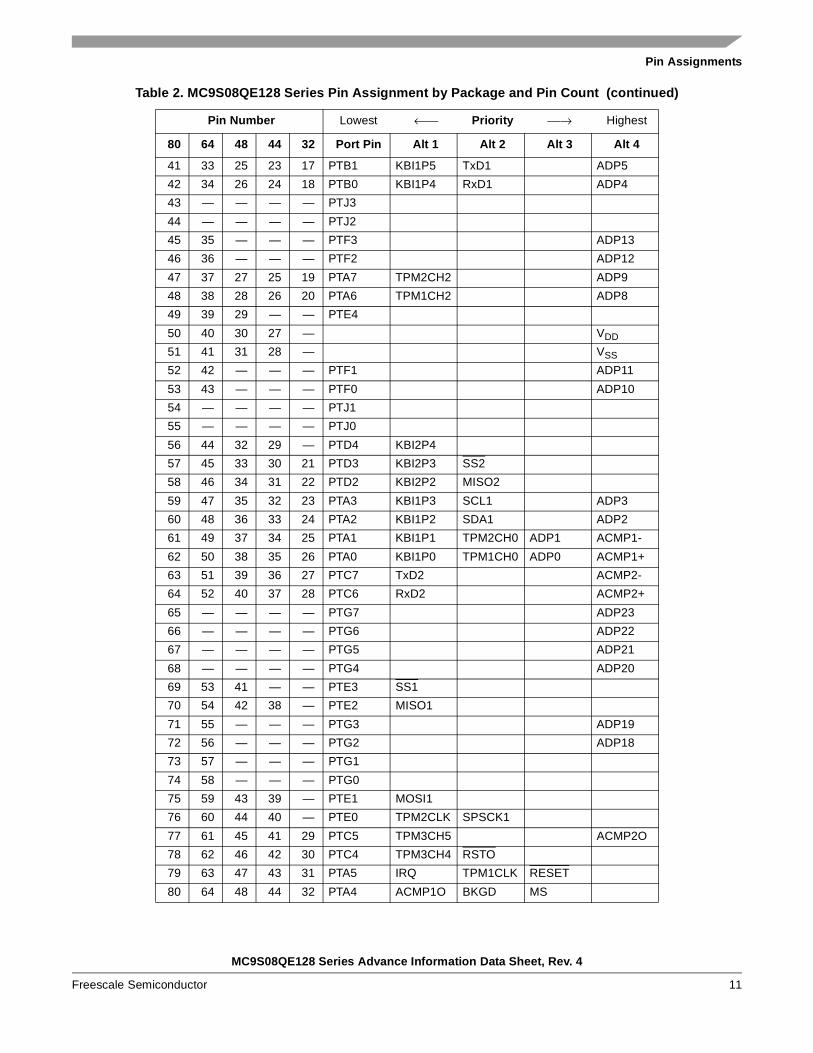
Pin Assignments
41 33 25 23 17 PTB1 KBI1P5 TxD1 ADP5
42 34 26 24 18 PTB0 KBI1P4 RxD1 ADP4
43 — — — — PTJ3
44 — — — — PTJ2
45 35 — — — PTF3 ADP13
46 36 — — — PTF2 ADP12
47 37 27 25 19 PTA7 TPM2CH2 ADP9
48 38 28 26 20 PTA6 TPM1CH2 ADP8
49 39 29 — — PTE4
50 40 30 27 — VDD
51 41 31 28 — VSS
52 42 — — — PTF1 ADP11
53 43 — — — PTF0 ADP10
54 — — — — PTJ1
55 — — — — PTJ0
56 44 32 29 — PTD4 KBI2P4
57 45 33 30 21 PTD3 KBI2P3 SS2
58 46 34 31 22 PTD2 KBI2P2 MISO2
59 47 35 32 23 PTA3 KBI1P3 SCL1 ADP3
60 48 36 33 24 PTA2 KBI1P2 SDA1 ADP2
61 49 37 34 25 PTA1 KBI1P1 TPM2CH0 ADP1 ACMP1-
62 50 38 35 26 PTA0 KBI1P0 TPM1CH0 ADP0 ACMP1+
63 51 39 36 27 PTC7 TxD2 ACMP2-
64 52 40 37 28 PTC6 RxD2 ACMP2+
65 — — — — PTG7 ADP23
66 — — — — PTG6 ADP22
67 — — — — PTG5 ADP21
68 — — — — PTG4 ADP20
69 53 41 — — PTE3 SS1
70 54 42 38 — PTE2 MISO1
71 55 — — — PTG3 ADP19
72 56 — — — PTG2 ADP18
73 57 — — — PTG1
74 58 — — — PTG0
75 59 43 39 — PTE1 MOSI1
76 60 44 40 — PTE0 TPM2CLK SPSCK1
77 61 45 41 29 PTC5 TPM3CH5 ACMP2O
78 62 46 42 30 PTC4 TPM3CH4 RSTO
79 63 47 43 31 PTA5 IRQ TPM1CLK RESET
80 64 48 44 32 PTA4 ACMP1O BKGD MS
Table 2. MC9S08QE128 Series Pin Assignment by Package and Pin Count (continued)
Pin Number Lowest ←⎯ Priority ⎯→ Highest
80 64 48 44 32 Port Pin Alt 1 Alt 2 Alt 3 Alt 4
MC9S08QE128 Series Advance Information Data Sheet, Rev. 4
Freescale Semiconductor 11

Electrical Characteristics
3 Electrical Characteristics
3.1 IntroductionThis section contains electrical and timing specifications for the MC9S08QE128 series of microcontrollers available at the time of publication.
3.2 Parameter ClassificationThe electrical parameters shown in this supplement are guaranteed by various methods. To give the customer a better understanding the following classification is used and the parameters are tagged accordingly in the tables where appropriate:
NOTEThe classification is shown in the column labeled “C” in the parameter tables where appropriate.
3.3 Absolute Maximum RatingsAbsolute maximum ratings are stress ratings only, and functional operation at the maxima is not guaranteed. Stress beyond the limits specified in Table 4 may affect device reliability or cause permanent damage to the device. For functional operating conditions, refer to the remaining tables in this section.
This device contains circuitry protecting against damage due to high static voltage or electrical fields; however, it is advised that normal precautions be taken to avoid application of any voltages higher than maximum-rated voltages to this high-impedance circuit. Reliability of operation is enhanced if unused inputs are tied to an appropriate logic voltage level (for instance, either VSS or VDD) or the programmable pull-up resistor associated with the pin is enabled.
Table 3. Parameter Classifications
P Those parameters are guaranteed during production testing on each individual device.
C Those parameters are achieved by the design characterization by measuring a statistically relevant sample size across process variations.
TThose parameters are achieved by design characterization on a small sample size from typical devices under typical conditions unless otherwise noted. All values shown in the typical column are within this category.
D Those parameters are derived mainly from simulations.
Table 4. Absolute Maximum Ratings
Rating Symbol Value Unit
Supply voltage VDD –0.3 to +3.8 V
Maximum current into VDD IDD 120 mA
Digital input voltage VIn –0.3 to VDD + 0.3 V
Instantaneous maximum current Single pin limit (applies to all port pins)1, 2, 3
1 Input must be current limited to the value specified. To determine the value of the required current-limiting resistor, calculate resistance values for positive (VDD) and negative (VSS) clamp voltages, then use the larger of the two resistance values.
2 All functional non-supply pins are internally clamped to VSS and VDD.
ID ± 25 mA
Storage temperature range Tstg –55 to 150 °C
MC9S08QE128 Series Advance Information Data Sheet, Rev. 4
Freescale Semiconductor12

Electrical Characteristics
3.4 Thermal CharacteristicsThis section provides information about operating temperature range, power dissipation, and package thermal resistance. Power dissipation on I/O pins is usually small compared to the power dissipation in on-chip logic and voltage regulator circuits, and it is user-determined rather than being controlled by the MCU design. To take PI/O into account in power calculations, determine the difference between actual pin voltage and VSS or VDD and multiply by the pin current for each I/O pin. Except in cases of unusually high pin current (heavy loads), the difference between pin voltage and VSS or VDD will be very small.
The average chip-junction temperature (TJ) in °C can be obtained from:
TJ = TA + (PD × θJA) Eqn. 1
where:
TA = Ambient temperature, °CθJA = Package thermal resistance, junction-to-ambient, °C/WPD = Pint + PI/O
3 Power supply must maintain regulation within operating VDD range during instantaneous and operating maximum current conditions. If positive injection current (VIn > VDD) is greater than IDD, the injection current may flow out of VDD and could result in external power supply going out of regulation. Ensure external VDD load will shunt current greater than maximum injection current. This will be the greatest risk when the MCU is not consuming power. Examples are: if no system clock is present, or if the clock rate is very low (which would reduce overall power consumption).
Table 5. Thermal Characteristics
Rating Symbol Value Unit
Operating temperature range (packaged)
TATL to TH
(–40 to 85 or 0 to 70)1
1 Depending on packaging.
°C
Maximum junction temperature TJM 95 °C
Thermal resistanceSingle-layer board
32-pin LQFP
θJA
82
°C/W44-pin LQFP 68
48-pin QFN 81
64-pin LQFPθJA
69°C/W
80-pin LQFP 60
Thermal resistanceFour-layer board
32-pin LQFP
θJA
54
°C/W44-pin LQFP 46
48-pin QFN 26
64-pin LQFPθJA
50°C/W
80-pin LQFP 47
MC9S08QE128 Series Advance Information Data Sheet, Rev. 4
Freescale Semiconductor 13

Electrical Characteristics
Pint = IDD × VDD, Watts — chip internal powerPI/O = Power dissipation on input and output pins — user determined
For most applications, PI/O << Pint and can be neglected. An approximate relationship between PD and TJ (if PI/O is neglected) is:
PD = K ÷ (TJ + 273°C) Eqn. 2
Solving Equation 1 and Equation 2 for K gives:
K = PD × (TA + 273°C) + θJA × (PD)2 Eqn. 3
where K is a constant pertaining to the particular part. K can be determined from equation 3 by measuring PD (at equilibrium) for a known TA. Using this value of K, the values of PD and TJ can be obtained by solving Equation 1 and Equation 2 iteratively for any value of TA.
3.5 ESD Protection and Latch-Up ImmunityAlthough damage from electrostatic discharge (ESD) is much less common on these devices than on early CMOS circuits, normal handling precautions should be used to avoid exposure to static discharge. Qualification tests are performed to ensure that these devices can withstand exposure to reasonable levels of static without suffering any permanent damage.
All ESD testing is in conformity with AEC-Q100 Stress Test Qualification for Automotive Grade Integrated Circuits. During the device qualification ESD stresses were performed for the human body model (HBM), the machine model (MM) and the charge device model (CDM).
A device is defined as a failure if after exposure to ESD pulses the device no longer meets the device specification. Complete DC parametric and functional testing is performed per the applicable device specification at room temperature followed by hot temperature, unless specified otherwise in the device specification.
Table 6. ESD and Latch-up Test Conditions
Model Description Symbol Value Unit
Human Body
Series resistance R1 1500 Ω
Storage capacitance C 100 pF
Number of pulses per pin — 3
Machine
Series resistance R1 0 Ω
Storage capacitance C 200 pF
Number of pulses per pin — 3
Latch-upMinimum input voltage limit – 2.5 V
Maximum input voltage limit 7.5 V
Table 7. ESD and Latch-Up Protection Characteristics
No. Rating1 Symbol Min Max Unit
1 Human body model (HBM) VHBM ± 2000 — V
2 Machine model (MM) VMM ± 200 — V
3 Charge device model (CDM) VCDM ± 500 — V
4 Latch-up current at TA = 85°C ILAT ± 100 — mA
MC9S08QE128 Series Advance Information Data Sheet, Rev. 4
Freescale Semiconductor14
Electrical Characteristics
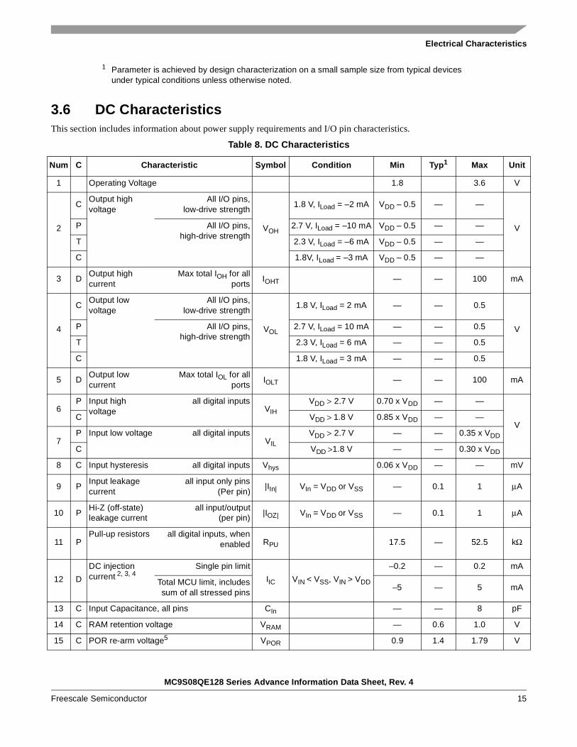
3.6 DC CharacteristicsThis section includes information about power supply requirements and I/O pin characteristics.
1 Parameter is achieved by design characterization on a small sample size from typical devices under typical conditions unless otherwise noted.
Table 8. DC Characteristics
Num C Characteristic Symbol Condition Min Typ1 Max Unit
1 Operating Voltage 1.8 3.6 V
2
COutput high voltage
All I/O pins,low-drive strength
VOH
1.8 V, ILoad = –2 mA VDD – 0.5 — —
VP All I/O pins,high-drive strength
2.7 V, ILoad = –10 mA VDD – 0.5 — —
T 2.3 V, ILoad = –6 mA VDD – 0.5 — —
C 1.8V, ILoad = –3 mA VDD – 0.5 — —
3 DOutput high current
Max total IOH for allports
IOHT — — 100 mA
4
COutput low voltage
All I/O pins,low-drive strength
VOL
1.8 V, ILoad = 2 mA — — 0.5
VP All I/O pins,high-drive strength
2.7 V, ILoad = 10 mA — — 0.5
T 2.3 V, ILoad = 6 mA — — 0.5
C 1.8 V, ILoad = 3 mA — — 0.5
DOutput low current
Max total IOL for allports
IOLT — — 100 mA5
6P Input high
voltageall digital inputs
VIH
VDD > 2.7 V 0.70 x VDD — —
VC VDD > 1.8 V 0.85 x VDD — —
7P Input low voltage all digital inputs
VIL
VDD > 2.7 V — — 0.35 x VDD
C VDD >1.8 V — — 0.30 x VDD
8 C Input hysteresis all digital inputs Vhys 0.06 x VDD — — mV
9 PInput leakage current
all input only pins(Per pin)
|IIn| VIn = VDD or VSS — 0.1 1 μA
10 PHi-Z (off-state) leakage current
all input/output(per pin)
|IOZ| VIn = VDD or VSS — 0.1 1 μA
11 PPull-up resistors all digital inputs, when
enabled RPU 17.5 — 52.5 kΩ
12 D
DC injection current 2, 3, 4
Single pin limit
IIC VIN < VSS, VIN > VDD
–0.2 — 0.2 mA
Total MCU limit, includessum of all stressed pins
–5 — 5 mA
13 C Input Capacitance, all pins CIn — — 8 pF
14 C RAM retention voltage VRAM — 0.6 1.0 V
15 C POR re-arm voltage5 VPOR 0.9 1.4 1.79 V
MC9S08QE128 Series Advance Information Data Sheet, Rev. 4
Freescale Semiconductor 15
Electrical Characteristics
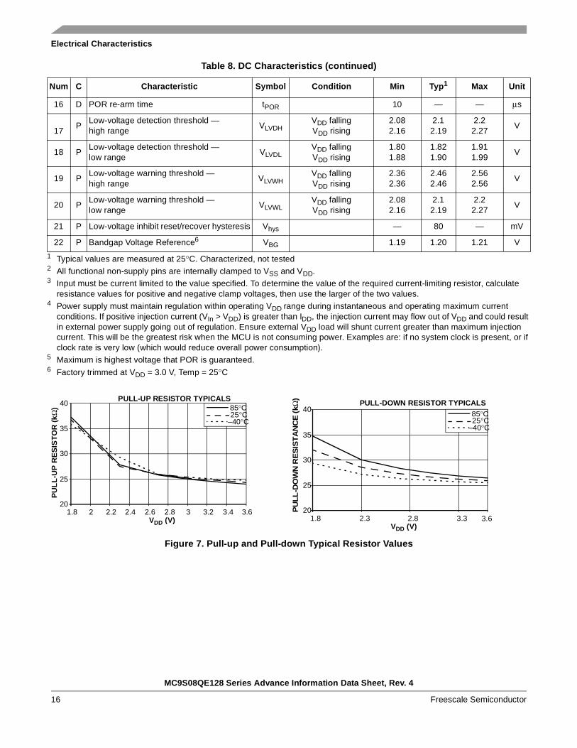
Figure 7. Pull-up and Pull-down Typical Resistor Values
16 D POR re-arm time tPOR 10 — — μs
17P
Low-voltage detection threshold —high range
VLVDHVDD fallingVDD rising
2.082.16
2.12.19
2.22.27
V
18 PLow-voltage detection threshold —low range
VLVDLVDD fallingVDD rising
1.801.88
1.821.90
1.911.99
V
19 PLow-voltage warning threshold —high range
VLVWHVDD fallingVDD rising
2.362.36
2.462.46
2.562.56
V
20 PLow-voltage warning threshold —low range
VLVWLVDD fallingVDD rising
2.082.16
2.12.19
2.22.27
V
21 P Low-voltage inhibit reset/recover hysteresis Vhys — 80 — mV
22 P Bandgap Voltage Reference6 VBG 1.19 1.20 1.21 V
1 Typical values are measured at 25°C. Characterized, not tested2 All functional non-supply pins are internally clamped to VSS and VDD.3 Input must be current limited to the value specified. To determine the value of the required current-limiting resistor, calculate
resistance values for positive and negative clamp voltages, then use the larger of the two values.4 Power supply must maintain regulation within operating VDD range during instantaneous and operating maximum current
conditions. If positive injection current (VIn > VDD) is greater than IDD, the injection current may flow out of VDD and could result in external power supply going out of regulation. Ensure external VDD load will shunt current greater than maximum injection current. This will be the greatest risk when the MCU is not consuming power. Examples are: if no system clock is present, or if clock rate is very low (which would reduce overall power consumption).
5 Maximum is highest voltage that POR is guaranteed.6 Factory trimmed at VDD = 3.0 V, Temp = 25°C
Table 8. DC Characteristics (continued)
Num C Characteristic Symbol Condition Min Typ1 Max Unit
PULL-UP RESISTOR TYPICALS
VDD (V)
PU
LL
-UP
RE
SIS
TO
R (
kΩ)
20
25
30
35
40
1.8 2 2.2 2.4 2.6 2.8 3 3.2 3.4 3.6
25°C85°C
–40°C
PULL-DOWN RESISTOR TYPICALS
VDD (V)
PU
LL
-DO
WN
RE
SIS
TA
NC
E (
kΩ)
20
25
30
35
40
1.8 2.3 2.8 3.3
25°C85°C
–40°C
3.6
MC9S08QE128 Series Advance Information Data Sheet, Rev. 4
Freescale Semiconductor16

Electrical Characteristics
Figure 8. Typical Low-Side Driver (Sink) Characteristics — Low Drive (PTxDSn = 0)
Figure 9. Typical Low-Side Driver (Sink) Characteristics — High Drive (PTxDSn = 1)
Figure 10. Typical High-Side (Source) Characteristics — Low Drive (PTxDSn = 0)
TYPICAL VOL VS IOL AT VDD = 3.0 V
IOL (mA)
VO
L (
V)
0
0.2
0.4
0.6
0.8
1
1.2
0 5 10 15 20
TYPICAL VOL VS VDD
VDD (V)
VO
L (
V)
0
0.05
0.1
0.15
0.2
1 2 3 4
25°C85°C
–40°C
25°C, IOL = 2 mA85°C, IOL = 2 mA
–40°C, IOL = 2 mA
TYPICAL VOL VS IOL AT VDD = 3.0 V
IOL (mA)
VO
L (
V)
0
0.2
0.4
0.6
0.8
1
0 10 20 30
TYPICAL VOL VS VDD
VDD (V)
VO
L (
V)
0
0.1
0.2
0.3
0.4
1 2 3 4
IOL = 6 mA
IOL = 3 mA
IOL = 10 mA
25°C85°C
–40°C 25°C85°C
–40°C
TYPICAL VDD – VOH VS IOH AT VDD = 3.0 V
IOH (mA))
0
0.2
0.4
0.6
0.8
1
1.2
–20–15–10–50
TYPICAL VDD – VOH VS VDD AT SPEC IOH
VDD (V)
VD
D –
VO
H (
V)
0
0.05
0.1
0.15
0.2
0.25
1 2 3 4
VD
D –
VO
H (
V) 25°C
85°C
–40°C 25°C, IOH = 2 mA85°C, IOH = 2 mA
–40°C, IOH = 2 mA
MC9S08QE128 Series Advance Information Data Sheet, Rev. 4
Freescale Semiconductor 17

Electrical Characteristics
Figure 11. Typical High-Side (Source) Characteristics — High Drive (PTxDSn = 1)
3.7 Supply Current CharacteristicsThis section includes information about power supply current in various operating modes.
Table 9. Supply Current Characteristics
Num C Parameter SymbolBusFreq
VDD (V)
Typ1 Max UnitTemp(°C)
1
P Run supply currentFEI mode, all modules on
RIDD
25.165 MHz
3
17.5 TBD
mA –40 to 85°CT 20 MHz 14.4 TBD
T 8 MHz 6.5 TBD
T 1 MHz 1.4 TBD
2
C Run supply currentFEI mode, all modules off
RIDD
25.165 MHz
3
11.5 TBD
mA –40 to 85°CT 20 MHz 9.5 TBD
T 8 MHz 4.6 TBD
T 1 MHz 1.0 TBD
3
TRun supply currentLPS=0, all modules off
RIDD
16 kHz FBILP
3
152 TBD
μA –40 to 85°CT
16 kHz FBELP
115 TBD
4
TRun supply currentLPS=1, all modules off, running from Flash
RIDD16 kHz FBELP
3
21.9TBD
μA
0 to 70°C
TBD –40 to 85°C
TRun supply currentLPS=1, all modules off, running from RAM
7.3TBD 0 to 70°C
TBD –40 to 85°C
5
C Wait mode supply currentFEI mode, all modules off
WIDD
25.165 MHz
3
5740 TBD
μA –-40 to 85°CT 20 MHz 4570 TBD
T 8 MHz 2000 TBD
T 1 MHz 730 TBD
TYPICAL VDD – VOH VS IOH AT VDD = 3.0 V
IOH (mA)
0
0.2
0.4
0.6
0.8
–30–25–20–15–10–50
TYPICAL VDD – VOH VS VDD AT SPEC IOH
VDD (V)
VD
D –
VO
H (
V)
0
0.1
0.2
0.3
0.4
1 2 3 4
IOH = –10 mA
IOH = –6 mA
IOH = –3 mAVD
D –
VO
H (
V)
25°C85°C
–40°C
25°C85°C
–40°C
MC9S08QE128 Series Advance Information Data Sheet, Rev. 4
Freescale Semiconductor18

Electrical Characteristics
6
Stop2 mode supply current
S2IDD
n/a
3 350TBD
nA
0 to 70°C
P TBD –40 to 85°C
2 250TBD 0 to 70°C
C TBD –40 to 85°C
7
Stop3 mode supply currentNo clocks active
S3IDD
n/a
3450
TBD
nA
0 to 70°C
P 3 TBD –40 to 85°C
2350
TBD 0 to 70°C
C 2 TBD –40 to 85°C
8 T
Low power mode adders:
EREFSTEN=1 32 kHz
3
500TBD
nA0 to 70°C
TBD –40 to 85°C
9 T IREFSTEN=1 32 kHz 70TBD
μA0 to 70°C
TBD –40 to 85°C
10 T TPM PWM 100 Hz 12TBD
μA0 to 70°C
TBD –40 to 85°C
11 T SCI, SPI, or IIC 300 bps 15TBD
μA0 to 70°C
TBD –40 to 85°C
12 T RTC using LPO 1 kHz 200TBD
nA0 to 70°C
TBD –40 to 85°C
13 TRTC using ICSERCLK
32 kHz 1TBD
μA0 to 70°C
TBD –40 to 85°C
14 T LVD n/a 100TBD
μA0 to 70°C
TBD –40 to 85°C
15 T ACMP n/a 20TBD
μA0 to 70°C
TBD –40 to 85°C1 Data in Typical column was characterized at 3.0 V, 25°C or is typical recommended value.
Table 9. Supply Current Characteristics (continued)
Num C Parameter SymbolBusFreq
VDD (V)
Typ1 Max UnitTemp(°C)
MC9S08QE128 Series Advance Information Data Sheet, Rev. 4
Freescale Semiconductor 19

Electrical Characteristics
Figure 12. Typical Run IDD for FBE and FEI, IDD vs. VDD (ACMP and ADC off, All Other Modules Enabled)
TBD
MC9S08QE128 Series Advance Information Data Sheet, Rev. 4
Freescale Semiconductor20

Electrical Characteristics
3.8 External Oscillator (XOSC) CharacteristicsReference Figure 13 and Figure 14 for crystal or resonator circuits.
Table 10. XOSC and ICS Specifications (Temperature Range = –40 to 85°C Ambient)
Num C Characteristic Symbol Min Typ1
1 Data in Typical column was characterized at 3.0 V, 25°C or is typical recommended value.
Max Unit
1 C
Oscillator crystal or resonator (EREFS = 1, ERCLKEN = 1)Low range (RANGE = 0)High range (RANGE = 1), high gain (HGO = 1)High range (RANGE = 1), low power (HGO = 0)
flofhifhi
3211
———
38.4168
kHzMHzMHz
2 DLoad capacitors
Low range (RANGE=0), low power (HGO=0)Other oscillator settings
C1,C2See Note2
See Note3
2 Load capacitors (C1,C2), feedback resistor (RF) and series resistor (RS) are incorporated internally when RANGE=HGO=0.3 See crystal or resonator manufacturer’s recommendation.
3 D
Feedback resistorLow range, low power (RANGE=0, HGO=0)2
Low range, High Gain (RANGE=0, HGO=1)High range (RANGE=1, HGO=X)
RF———
—101
———
MΩ
4 D
Series resistor — Low range, low power (RANGE = 0, HGO = 0)2
Low range, high gain (RANGE = 0, HGO = 1)High range, low power (RANGE = 1, HGO = 0)High range, high gain (RANGE = 1, HGO = 1)
≥ 8 MHz4 MHz1 MHz
RS
———
———
—0
100
000
———
01020
kΩ
5 C
Crystal start-up time 4
Low range, low powerLow range, high powerHigh range, low powerHigh range, high power
4 Proper PC board layout procedures must be followed to achieve specifications.
tCSTL
tCSTH
————
200400
515
————
ms
6 DSquare wave input clock frequency (EREFS = 0, ERCLKEN = 1)
FEE mode FBE or FBELP mode
fextal 0.031250
——
50.3350.33
MHzMHz
MC9S08QE128 Series Advance Information Data Sheet, Rev. 4
Freescale Semiconductor 21

Electrical Characteristics
Figure 13. Typical Crystal or Resonator Circuit: High Range and Low Range/High Gain
Figure 14. Typical Crystal or Resonator Circuit: Low Range/Low Gain
3.9 Internal Clock Source (ICS) CharacteristicsTable 11. ICS Frequency Specifications (Temperature Range = –40 to 85°C Ambient)
Num C Characteristic Symbol Min Typ1 Max Unit
1 PAverage internal reference frequency — factory trimmed
at VDD = 3.6 V and temperature = 25°Cfint_ft — 32.768 — kHz
2 P Internal reference frequency — user trimmed fint_ut 31.25 — 39.06 kHz
3 T Internal reference start-up time tIRST — 60 100 μs
4
PDCO output frequency range —
trimmed 2
Low range (DRS=00)
fdco_u
16 — 20
MHzC Mid range (DRS=01) 32 — 40
P High range (DRS=10) 48 — 60
5
P DCO output frequency 2
Reference = 32768 Hz and
DMX32 = 1
Low range (DRS=00)
fdco_DMX32
— 19.92 —
MHzP Mid range (DRS=01) — 39.85 —
P High range (DRS=10) — 59.77 —
6 CResolution of trimmed DCO output frequency at fixed voltage and temperature (using FTRIM)
Δfdco_res_t — ± 0.1 ± 0.2 %fdco
7 CResolution of trimmed DCO output frequency at fixed voltage and temperature (not using FTRIM)
Δfdco_res_t — ± 0.2 ± 0.4 %fdco
XOSC
EXTAL XTAL
Crystal or Resonator
RS
C2
RF
C1
XOSC
EXTAL XTAL
Crystal or Resonator
MC9S08QE128 Series Advance Information Data Sheet, Rev. 4
Freescale Semiconductor22

Electrical Characteristics
Figure 15. Deviation of DCO Output from Trimmed Frequency (50.33 MHz, 3.0 V)
8 CTotal deviation of trimmed DCO output frequency over voltage and temperature
Δfdco_t —+ 0.5-1.0
± 2 %fdco
9 CTotal deviation of trimmed DCO output frequency over fixed voltage and temperature range of 0°C to 70 °C
Δfdco_t — ± 0.5 ± 1 %fdco
10 C FLL acquisition time 3 tAcquire — — 1 ms
11 CLong term jitter of DCO output clock (averaged over 2-ms
interval) 4CJitter — 0.02 0.2 %fdco
1 Data in Typical column was characterized at 3.0 V, 25°C or is typical recommended value.2 The resulting bus clock frequency should not exceed the maximum specified bus clock frequency of the device.3 This specification applies to any time the FLL reference source or reference divider is changed, trim value changed or changing
from FLL disabled (FBELP, FBILP) to FLL enabled (FEI, FEE, FBE, FBI). If a crystal/resonator is being used as the reference, this specification assumes it is already running.
4 Jitter is the average deviation from the programmed frequency measured over the specified interval at maximum fBus. Measurements are made with the device powered by filtered supplies and clocked by a stable external clock signal. Noise injected into the FLL circuitry via VDD and VSS and variation in crystal oscillator frequency increase the CJitter percentage for a given interval.
Table 11. ICS Frequency Specifications (Temperature Range = –40 to 85°C Ambient) (continued)
Num C Characteristic Symbol Min Typ1 Max Unit
TBD
MC9S08QE128 Series Advance Information Data Sheet, Rev. 4
Freescale Semiconductor 23
Electrical Characteristics
Figure 16. Deviation of DCO Output from Trimmed Frequency (50.33 MHz, 25°C)
3.10 AC CharacteristicsThis section describes timing characteristics for each peripheral system.
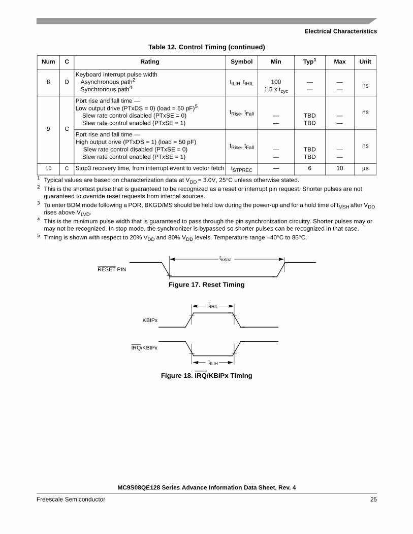
3.10.1 Control Timing
Table 12. Control Timing
Num C Rating Symbol Min Typ1 Max Unit
1 DBus frequency (tcyc = 1/fBus)
VDD ≤ 2.1VVDD > 2.1V
fBus dcdc
——
1025.165
MHz
2 D Internal low power oscillator period tLPO 700 — 1300 μs
3 D External reset pulse width2 textrst 100 — — ns
4 D Reset low drive trstdrv 34 x tcyc — — ns
5 DBKGD/MS setup time after issuing background debug force reset to enter user or BDM modes
tMSSU 500 — — ns
6 DBKGD/MS hold time after issuing background debug force reset to enter user or BDM modes 3
tMSH 100 — — μs
7 DIRQ pulse width
Asynchronous path2
Synchronous path4tILIH, tIHIL 100
1.5 x tcyc
——
——
ns
TBD
MC9S08QE128 Series Advance Information Data Sheet, Rev. 4
Freescale Semiconductor24
Electrical Characteristics
Figure 17. Reset Timing
Figure 18. IRQ/KBIPx Timing
8 DKeyboard interrupt pulse width
Asynchronous path2
Synchronous path4tILIH, tIHIL 100
1.5 x tcyc
——
——
ns
9 C
Port rise and fall time — Low output drive (PTxDS = 0) (load = 50 pF)5
Slew rate control disabled (PTxSE = 0) Slew rate control enabled (PTxSE = 1)
tRise, tFall ——
TBDTBD
——
ns
Port rise and fall time — High output drive (PTxDS = 1) (load = 50 pF)
Slew rate control disabled (PTxSE = 0) Slew rate control enabled (PTxSE = 1)
tRise, tFall ——
TBDTBD
——
ns
10 C Stop3 recovery time, from interrupt event to vector fetch tSTPREC — 6 10 μs
1 Typical values are based on characterization data at VDD = 3.0V, 25°C unless otherwise stated.2 This is the shortest pulse that is guaranteed to be recognized as a reset or interrupt pin request. Shorter pulses are not
guaranteed to override reset requests from internal sources.3 To enter BDM mode following a POR, BKGD/MS should be held low during the power-up and for a hold time of tMSH after VDD
rises above VLVD.4 This is the minimum pulse width that is guaranteed to pass through the pin synchronization circuitry. Shorter pulses may or
may not be recognized. In stop mode, the synchronizer is bypassed so shorter pulses can be recognized in that case.5 Timing is shown with respect to 20% VDD and 80% VDD levels. Temperature range –40°C to 85°C.
Table 12. Control Timing (continued)
Num C Rating Symbol Min Typ1 Max Unit
textrst
RESET PIN
tIHIL
KBIPx
tILIH
IRQ/KBIPx
MC9S08QE128 Series Advance Information Data Sheet, Rev. 4
Freescale Semiconductor 25

Electrical Characteristics
3.10.2 TPM Module TimingSynchronizer circuits determine the shortest input pulses that can be recognized or the fastest clock that can be used as the optional external source to the timer counter. These synchronizers operate from the current bus rate clock.
Figure 19. Timer External Clock
Figure 20. Timer Input Capture Pulse
Table 13. TPM Input Timing
No. C Function Symbol Min Max Unit
1 D External clock frequency fTCLK 0 fBus/4 Hz
2 D External clock period tTCLK 4 — tcyc
3 D External clock high time tclkh 1.5 — tcyc
4 D External clock low time tclkl 1.5 — tcyc
5 D Input capture pulse width tICPW 1.5 — tcyc
tTCLK
tclkh
tclkl
TCLK
tICPW
TPMCHn
tICPW
TPMCHn
MC9S08QE128 Series Advance Information Data Sheet, Rev. 4
Freescale Semiconductor26

Electrical Characteristics
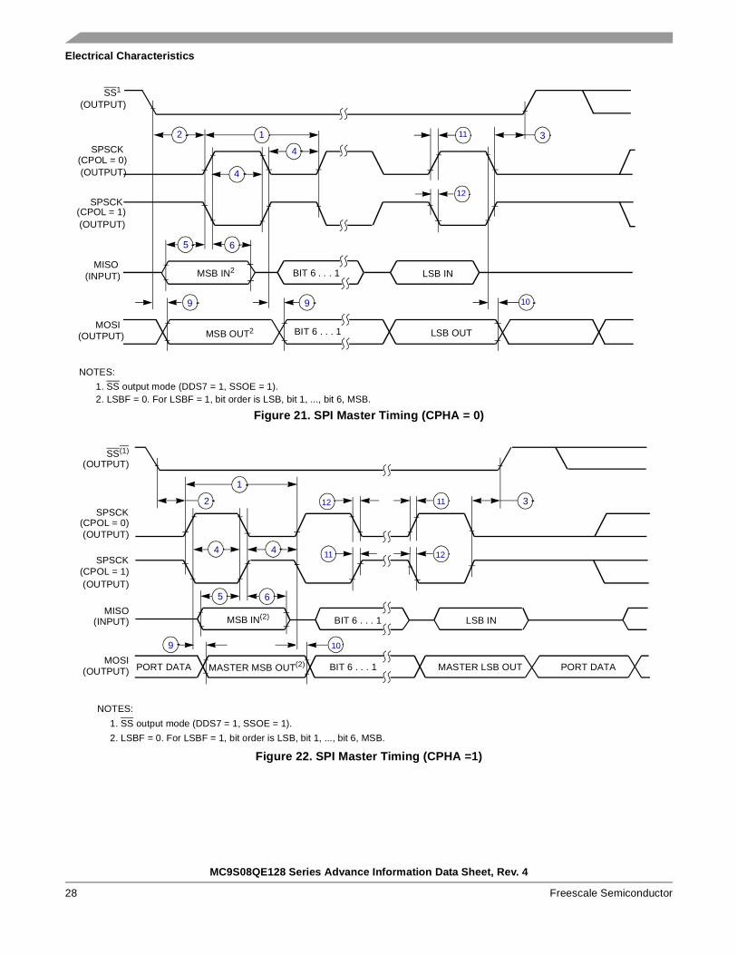
3.10.3 SPI TimingTable 14 and Figure 21 through Figure 24 describe the timing requirements for the SPI system.
Table 14. SPI Timing
No. C Function Symbol Min Max Unit
— DOperating frequency
MasterSlave
fopfBus/2048
0fBus/2fBus/4
HzHz
1 DSPSCK period
MasterSlave
tSPSCK24
2048—
tcyctcyc
2 DEnable lead time
MasterSlave
tLead1/21
——
tSPSCKtcyc
3 DEnable lag time
MasterSlave
tLag1/21
——
tSPSCKtcyc
4 DClock (SPSCK) high or low time
MasterSlave
tWSPSCKtcyc – 30tcyc – 30
1024 tcyc—
nsns
5 DData setup time (inputs)
MasterSlave
tSU1515
——
nsns
6 DData hold time (inputs)
MasterSlave
tHI025
——
nsns
7 D Slave access time ta — 1 tcyc
8 D Slave MISO disable time tdis — 1 tcyc
9 DData valid (after SPSCK edge)
MasterSlave
tv——
2525
nsns
10 DData hold time (outputs)
MasterSlave
tHO00
——
nsns
11 DRise time
InputOutput
tRItRO
——
tcyc – 2525
nsns
12 DFall time
InputOutput
tFItFO
——
tcyc – 2525
nsns
MC9S08QE128 Series Advance Information Data Sheet, Rev. 4
Freescale Semiconductor 27
Electrical Characteristics
Figure 21. SPI Master Timing (CPHA = 0)
Figure 22. SPI Master Timing (CPHA =1)
SPSCK
(OUTPUT)
SPSCK
(OUTPUT)
MISO(INPUT)
MOSI(OUTPUT)
SS1
(OUTPUT)
MSB IN2
BIT 6 . . . 1
LSB IN
MSB OUT2 LSB OUT
BIT 6 . . . 1
(CPOL = 0)
(CPOL = 1)
NOTES:
2. LSBF = 0. For LSBF = 1, bit order is LSB, bit 1, ..., bit 6, MSB.1. SS output mode (DDS7 = 1, SSOE = 1).
12 3
4
5 6
9 10
11
12
4
9
SPSCK
(OUTPUT)
SPSCK
(OUTPUT)
MISO(INPUT)
MOSI(OUTPUT)
MSB IN(2)
BIT 6 . . . 1
LSB IN
MASTER MSB OUT(2) MASTER LSB OUT
BIT 6 . . . 1
PORT DATA
(CPOL = 0)
(CPOL = 1)
PORT DATA
SS(1)
(OUTPUT)
1. SS output mode (DDS7 = 1, SSOE = 1).
2. LSBF = 0. For LSBF = 1, bit order is LSB, bit 1, ..., bit 6, MSB.
NOTES:
2
1
12 11 3
4 4 11 12
5 6
9 10
MC9S08QE128 Series Advance Information Data Sheet, Rev. 4
Freescale Semiconductor28

Electrical Characteristics
Figure 23. SPI Slave Timing (CPHA = 0)
Figure 24. SPI Slave Timing (CPHA = 1)
SPSCK
(INPUT)
SPSCK
(INPUT)
MOSI(INPUT)
MISO(OUTPUT)
SS(INPUT)
MSB IN
BIT 6 . . . 1
LSB IN
MSB OUT SLAVE LSB OUT
BIT 6 . . . 1
(CPOL = 0)
(CPOL = 1)
NOTE:
SLAVESEE
NOTE
1. Not defined but normally MSB of character just received
1
2
3
4
5 6
7
8
9 10
1112
4 11 12
10
SPSCK
(INPUT)
SPSCK
(INPUT)
MOSI(INPUT)
MISO(OUTPUT)
MSB IN
BIT 6 . . . 1
LSB IN
MSB OUT SLAVE LSB OUT
BIT 6 . . . 1
SEE
(CPOL = 0)
(CPOL = 1)
SS(INPUT)
NOTE:
SLAVE NOTE
1. Not defined but normally LSB of character just received
1
2
3
4
5 67
89 10
1112
4 11 12
MC9S08QE128 Series Advance Information Data Sheet, Rev. 4
Freescale Semiconductor 29

Electrical Characteristics
3.10.4 Analog Comparator (ACMP) Electricals
3.10.5 ADC Characteristics
Table 15. Analog Comparator Electrical Specifications
C Characteristic Symbol Min Typical Max Unit
D Supply voltage VDD 1.80 — 3.6 V
P Supply current (active) IDDAC — 20 35 μA
D Analog input voltage VAIN VSS – 0.3 — VDD V
P Analog input offset voltage VAIO 20 40 mV
C Analog comparator hysteresis VH 3.0 9.0 15.0 mV
P Analog input leakage current IALKG — — 1.0 μA
C Analog comparator initialization delay tAINIT — — 1.0 μs
Table 16. 12-bit ADC Operating Conditions
C Characteristic Conditions Symb Min Typ1
1 Typical values assume VDDAD = 3.0V, Temp = 25°C, fADCK=1.0MHz unless otherwise stated. Typical values are for reference only and are not tested in production.
Max Unit Comment
DSupply voltage Absolute VDDAD 1.8 — 3.6 V
Delta to VDD (VDD-VDDAD)2
2 DC potential difference.
ΔVDDAD -100 0 +100 mV
D Ground voltage Delta to VSS (VSS-VSSAD)2 ΔVSSAD -100 0 +100 mV
D Ref Voltage High VREFH 1.8 VDDAD VDDAD V
D Ref Voltage Low VREFL VSSAD VSSAD VSSAD V
D Input Voltage VADIN VREFL — VREFH V
CInput Capacitance
CADIN — 4.5 5.5pF
C Input Resistance RADIN — 5 7 kΩ
C
Analog Source Resistance
12 bit modefADCK > 4MHzfADCK < 4MHz
RAS——
——
25
kΩ
External to MCU
10 bit modefADCK > 4MHzfADCK < 4MHz
——
——
510
8 bit mode (all valid fADCK) — — 10
DADC Conversion Clock Freq.
High Speed (ADLPC=0) fADCK 0.4 — 8.0MHz
Low Power (ADLPC=1) 0.4 — 4.0
MC9S08QE128 Series Advance Information Data Sheet, Rev. 4
Freescale Semiconductor30

Electrical Characteristics
Figure 25. ADC Input Impedance Equivalency Diagram
Table 17. 12-bit ADC Characteristics (VREFH = VDDAD, VREFL = VSSAD)
Characteristic Conditions C Symb Min Typ1 Max Unit Comment
Supply CurrentADLPC=1ADLSMP=1ADCO=1
T IDDAD — 120 —
μA
Supply CurrentADLPC=1ADLSMP=0ADCO=1
T IDDAD — 202 —
μA
Supply CurrentADLPC=0ADLSMP=1ADCO=1
T IDDAD — 288 —
μA
Supply CurrentADLPC=0ADLSMP=0ADCO=1
P IDDAD — 0.532 1
mA
Supply Current Stop, Reset, Module Off IDDAD — 0.007 0.8 μA
ADC Asynchronous Clock Source
High Speed (ADLPC=0) P fADACK 2 3.3 5MHz
tADACK = 1/fADACK
Low Power (ADLPC=1) C 1.25 2 3.3
+–
+
–VAS
RAS
CAS
VADIN
ZASPad leakagedue toinput protection
ZADIN
SIMPLIFIED INPUT PIN EQUIVALENT
CIRCUIT
RADIN
ADC SARENGINE
SIMPLIFIED CHANNEL SELECT
CIRCUIT
INPUT PIN
RADIN
CADIN
INPUT PIN
RADIN
INPUT PIN
RADIN
MC9S08QE128 Series Advance Information Data Sheet, Rev. 4
Freescale Semiconductor 31

Electrical Characteristics
Conversion Time (Including sample time)
Short Sample (ADLSMP=0) P tADC — 20 — ADCK cycles
See the ADC chapter in the
MC9S08QE128 Reference Manual for conversion time
variances
Long Sample (ADLSMP=1) C — 40 —
Sample Time Short Sample (ADLSMP=0) P tADS — 3.5 — ADCK cycles
Long Sample (ADLSMP=1) C — 23.5 —
Total Unadjusted Error
12 bit mode T ETUE — ±3.0 — LSB2 Includes Quantization
10 bit mode P — ±1 ±2.5
8 bit mode T — ±0.5 ±1.0
Differential Non-Linearity
12 bit mode T DNL — ±1.75 — LSB2
10 bit mode3 P — ±0.5 ±1.0
8 bit mode3 T — ±0.3 ±0.5
Integral Non-Linearity
12 bit mode T INL — ±1.5 — LSB2
10 bit mode P — ±0.5 ±1.0
8 bit mode T — ±0.3 ±0.5
Zero-Scale Error 12 bit mode T EZS — ±1.5 — LSB2 VADIN = VSSAD
10 bit mode P — ±0.5 ±1.5
8 bit mode T — ±0.5 ±0.5
Full-Scale Error 12 bit mode T EFS — ±1.0 — LSB2 VADIN = VDDAD
10 bit mode P — ±0.5 ±1
8 bit mode T — ±0.5 ±0.5
Quantization Error
12 bit mode D EQ — -1 to 0 — LSB2
10 bit mode — — ±0.5
8 bit mode — — ±0.5
Input Leakage Error
12 bit mode D EIL — ±2 — LSB2 Pad leakage4 * RAS
10 bit mode — ±0.2 ±4
8 bit mode — ±0.1 ±1.2
Temp SensorSlope
-40°C to 25°C D m — 1.646 — mV/°C
25°C to 85°C — 1.769 —
Temp SensorVoltage
25°C D VTEMP25 — 701.2 — mV
1 Typical values assume VDDAD = 3.0V, Temp = 25°C, fADCK=1.0MHz unless otherwise stated. Typical values are for reference only and are not tested in production.
2 1 LSB = (VREFH - VREFL)/2N
3 Monotonicity and No-Missing-Codes guaranteed in 10 bit and 8 bit modes4 Based on input pad leakage current. Refer to pad electricals.
Table 17. 12-bit ADC Characteristics (VREFH = VDDAD, VREFL = VSSAD) (continued)
Characteristic Conditions C Symb Min Typ1 Max Unit Comment
MC9S08QE128 Series Advance Information Data Sheet, Rev. 4
Freescale Semiconductor32

Electrical Characteristics
3.10.6 Flash SpecificationsThis section provides details about program/erase times and program-erase endurance for the flash memory.
Program and erase operations do not require any special power sources other than the normal VDD supply. For more detailed information about program/erase operations, see the Memory section of the MC9S08QE128 Reference Manual.
3.11 EMC PerformanceElectromagnetic compatibility (EMC) performance is highly dependent on the environment in which the MCU resides. Board design and layout, circuit topology choices, location and characteristics of external components as well as MCU software operation all play a significant role in EMC performance. The system designer should consult Freescale applications notes such as AN2321, AN1050, AN1263, AN2764, and AN1259 for advice and guidance specifically targeted at optimizing EMC performance.
Table 18. Flash Characteristics
C Characteristic Symbol Min Typical Max Unit
DSupply voltage for program/erase-40°C to 85°C Vprog/erase 1.8 3.6 V
D Supply voltage for read operation VRead 1.8 3.6 V
D Internal FCLK frequency1
1 The frequency of this clock is controlled by a software setting.
fFCLK 150 200 kHz
D Internal FCLK period (1/FCLK) tFcyc 5 6.67 μs
P Byte program time (random location)(2) tprog 9 tFcyc
P Byte program time (burst mode)(2) tBurst 4 tFcyc
P Page erase time2
2 These values are hardware state machine controlled. User code does not need to count cycles. This information supplied for calculating approximate time to program and erase.
tPage 4000 tFcyc
P Mass erase time(2) tMass 20,000 tFcyc
Byte program current3
3 The program and erase currents are additional to the standard run IDD. These values are measured at room temperatures with VDD = 3.0 V, bus frequency = 4.0 MHz.
RIDDBP — 4 — mA
Page erase current3 RIDDPE — 6 — mA
CProgram/erase endurance4
TL to TH = –40°C to + 85°CT = 25°C
4 Typical endurance for flash was evaluated for this product family on the HC9S12Dx64. For additional information on how Freescale defines typical endurance, please refer to Engineering Bulletin EB619, Typical Endurance for Nonvolatile Memory.
10,000—
—100,000
——
cycles
C Data retention5
5 Typical data retention values are based on intrinsic capability of the technology measured at high temperature and de-rated to 25°C using the Arrhenius equation. For additional information on how Freescale defines typical data retention, please refer to Engineering Bulletin EB618, Typical Data Retention for Nonvolatile Memory.
tD_ret 15 100 — years
MC9S08QE128 Series Advance Information Data Sheet, Rev. 4
Freescale Semiconductor 33
Electrical Characteristics
3.11.1 Radiated EmissionsMicrocontroller radiated RF emissions are measured from 150 kHz to 1 GHz using the TEM/GTEM Cell method in accordance with the IEC 61967-2 and SAE J1752/3 standards. The measurement is performed with the microcontroller installed on a custom EMC evaluation board while running specialized EMC test software. The radiated emissions from the microcontroller are measured in a TEM cell in two package orientations (North and East).
The maximum radiated RF emissions of the tested configuration in all orientations are less than or equal to the reported emissions levels.
3.11.2 Conducted Transient SusceptibilityMicrocontroller transient conducted susceptibility is measured in accordance with an internal Freescale test method. The measurement is performed with the microcontroller installed on a custom EMC evaluation board and running specialized EMC test software designed in compliance with the test method. The conducted susceptibility is determined by injecting the transient susceptibility signal on each pin of the microcontroller. The transient waveform and injection methodology is based on IEC 61000-4-4 (EFT/B). The transient voltage required to cause performance degradation on any pin in the tested configuration is greater than or equal to the reported levels unless otherwise indicated by footnotes below Table 20.
Table 19. Radiated Emissions, Electric Field
Parameter Symbol Conditions Frequency fOSC/fBUSLevel1
(Max)
1 Data based on qualification test results.
Unit
Radiated emissions,electric field
VRE_TEM
VDD = TBDTA = +25oC
package typeTBD
0.15 – 50 MHz
TBD crystalTBD bus
TBD
dBμV50 – 150 MHz TBD
150 – 500 MHz TBD
500 – 1000 MHz TBD
IEC Level TBD —
SAE Level TBD —
Table 20. Conducted Susceptibility, EFT/B
Parameter Symbol Conditions fOSC/fBUS Result Amplitude1
(Min)
1 Data based on qualification test results. Not tested in production.
Unit
Conducted susceptibility, electrical fast transient/burst (EFT/B)
VCS_EFT
VDD = TBDTA = +25oC
package typeTBD
TBD crystalTBD bus
A TBD
kVB TBD
C TBD
D TBD
MC9S08QE128 Series Advance Information Data Sheet, Rev. 4
Freescale Semiconductor34
Ordering Information
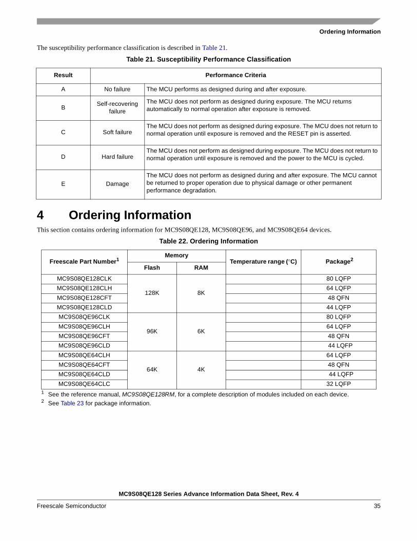
The susceptibility performance classification is described in Table 21.
4 Ordering InformationThis section contains ordering information for MC9S08QE128, MC9S08QE96, and MC9S08QE64 devices.
Table 21. Susceptibility Performance Classification
Result Performance Criteria
A No failure The MCU performs as designed during and after exposure.
BSelf-recovering
failure
The MCU does not perform as designed during exposure. The MCU returns automatically to normal operation after exposure is removed.
C Soft failureThe MCU does not perform as designed during exposure. The MCU does not return to normal operation until exposure is removed and the RESET pin is asserted.
D Hard failureThe MCU does not perform as designed during exposure. The MCU does not return to normal operation until exposure is removed and the power to the MCU is cycled.
E DamageThe MCU does not perform as designed during and after exposure. The MCU cannot be returned to proper operation due to physical damage or other permanent performance degradation.
Table 22. Ordering Information
Freescale Part Number1
1 See the reference manual, MC9S08QE128RM, for a complete description of modules included on each device.
MemoryTemperature range (°C) Package2
2 See Table 23 for package information.
Flash RAM
MC9S08QE128CLK
128K 8K
80 LQFP
MC9S08QE128CLH 64 LQFP
MC9S08QE128CFT 48 QFN
MC9S08QE128CLD 44 LQFP
MC9S08QE96CLK
96K 6K
80 LQFP
MC9S08QE96CLH 64 LQFP
MC9S08QE96CFT 48 QFN
MC9S08QE96CLD 44 LQFP
MC9S08QE64CLH
64K 4K
64 LQFP
MC9S08QE64CFT 48 QFN
MC9S08QE64CLD 44 LQFP
MC9S08QE64CLC 32 LQFP
MC9S08QE128 Series Advance Information Data Sheet, Rev. 4
Freescale Semiconductor 35

Package Information
4.1 Device Numbering SystemExample of the device numbering system:
5 Package InformationThe below table details the various packages available.
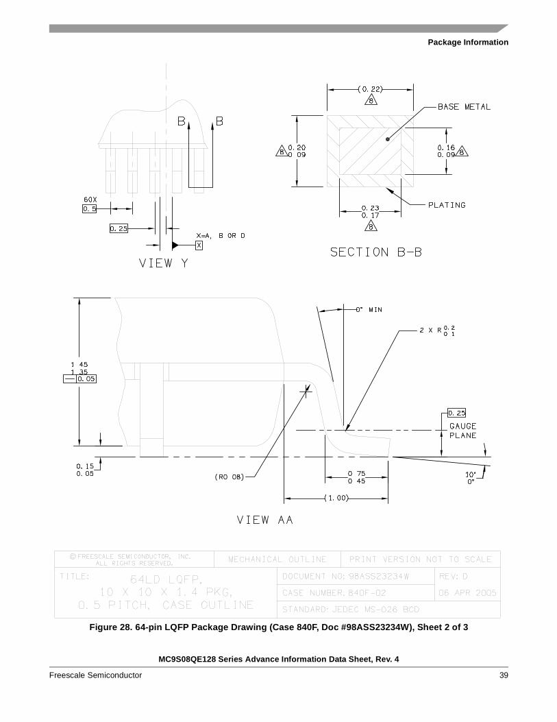
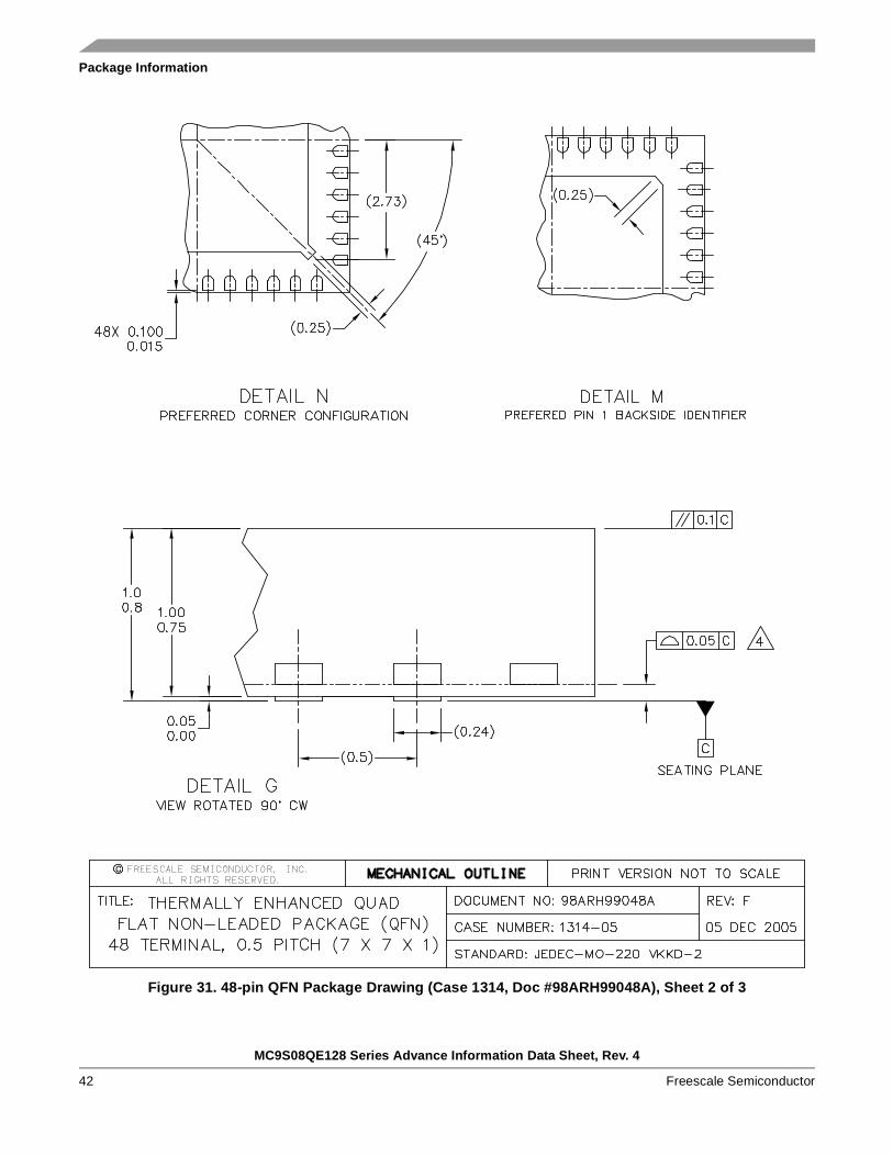
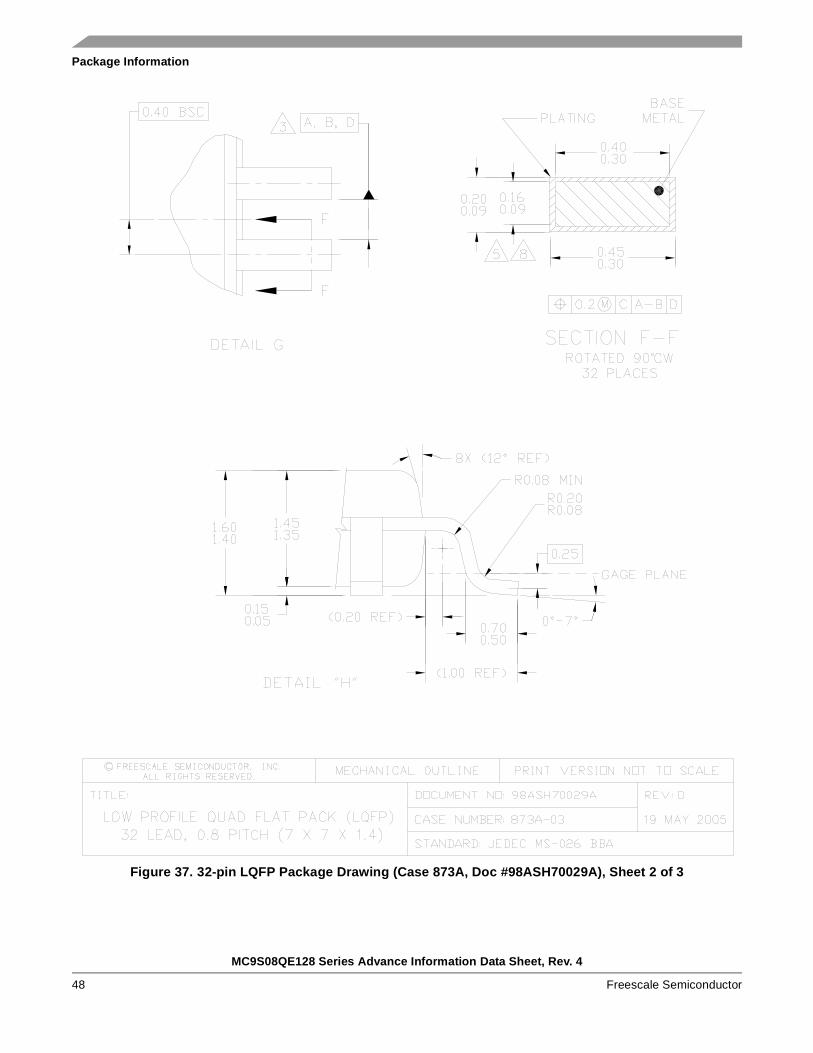
5.1 Mechanical DrawingsThe following pages are mechanical drawings for the packages described in Table 23. For the latest available drawings please visit our web site (http://www.freescale.com) and enter the package’s document number into the keyword search box.
Table 23. Package Descriptions
Pin Count Package Type Abbreviation Designator Case No. Document No.
80 Low Quad Flat Package LQFP LK 917A 98ASS23237W
64 Low Quad Flat Package LQFP LH 840F 98ASS23234W
48 Quad Flat No-Leads QFN FT 1314 98ARH99048A
44 Low Quad Flat Package LQFP LD 824D 98ASS23225W
32 Low Quad Flat Package LQFP LC 873A 98ASH70029A
MC
Temperature range
Family
Memory
Status
Core
(C = –40°C to 85°C)(9 = Flash-based)
9 S08 XX
(MC = Fully Qualified) Package designator (see Table 23)
Approximate flash size in Kbytes
QE 128 C
MC9S08QE128 Series Advance Information Data Sheet, Rev. 4
Freescale Semiconductor36

Package Information
Figure 26. 80-pin LQFP Package Drawing (Case 917A, Doc #98ASS23237W)
1
20
21 40
41
60
6180
VIEW AA
ÍÍÍÍÍÍÍÍÇÇÇÇÇÇ
NOTES:1. DIMENSIONING AND TOLERANCING PER ANSI
Y14.5M, 1982.2. CONTROLLING DIMENSION: MILLIMETER.3. DATUM PLANE –H– IS LOCATED AT BOTTOM OF
LEAD AND IS COINCIDENT WITH THE LEADWHERE THE LEAD EXITS THE PLASTIC BODY ATTHE BOTTOM OF THE PARTING LINE.
4. DATUMS –L–, –M– AND –N– TO BE DETERMINEDAT DATUM PLANE –H–.
5. DIMENSIONS S AND V TO BE DETERMINED ATSEATING PLANE –T–.
6. DIMENSIONS A AND B DO NOT INCLUDE MOLDPROTRUSION. ALLOWABLE PROTRUSION IS0.250 (0.010) PER SIDE. DIMENSIONS A AND BDO INCLUDE MOLD MISMATCH AND AREDETERMINED AT DATUM PLANE –H–.
7. DIMENSION D DOES NOT INCLUDE DAMBARPROTRUSION. DAMBAR PROTRUSION SHALLNOT CAUSE THE LEAD WIDTH TO EXCEED 0.460(0.018). MINIMUM SPACE BETWEENPROTRUSION AND ADJACENT LEAD ORPROTRUSION 0.07 (0.003).
AB
VIEW Y
(K)
(Z)
(W)
VIEW AA
DIMA
MIN MAX MIN MAXINCHES
14.00 BSC 0.551 BSC
MILLIMETERS
A1 7.00 BSC 0.276 BSCB 14.00 BSC 0.551 BSCB1 7.00 BSC 0.276 BSCC ––– 1.60 ––– 0.063C1 0.04 0.24 0.002 0.009C2 1.30 1.50 0.051 0.059D 0.22 0.38 0.009 0.015E 0.40 0.75 0.016 0.030F 0.17 0.33 0.007 0.013G 0.65 BSC 0.026 BSCJ 0.09 0.27 0.004 0.011K 0.50 REF 0.020 REFP 0.325 BSC 0.013 REF
R1 0.10 0.20 0.004 0.008S 16.00 BSC 0.630 BSCS1 8.00 BSC 0.315 BSCU 0.09 0.16 0.004 0.006V 16.00 BSC 0.630 BSCV1 8.00 BSC 0.315 BSCW 0.20 REF 0.008 REFZ 1.00 REF 0.039 REF001 ––– –––02
C2
C1
CL
0 10 09 14
0 10 09 14
L–M0.20 (0.008) H N
4X
3X VIEW Y–L–
L–M0.20 (0.008) T N
–M–
B V
V1B1
–N–
S1
A1
SA
4X 20 TIPS
SEATING
0.10 (0.004) T–H–
PLANE
–T–
8XC
2
GAGE
0.25 (0.010)
PLANE
2X R R1
E
1
S0.05 (0.002)
AB
–X–X= L, M, N
P
G
PLATING
BASEMETALJ
U
F
D
SECTION AB–AB
SL–MM0.13 (0.005) N ST
ROTATED 90 CLOCKWISE
CASE 917A-02ISSUE C
DATE 09/21/95
MC9S08QE128 Series Advance Information Data Sheet, Rev. 4
Freescale Semiconductor 37

Package Information
Figure 27. 64-pin LQFP Package Drawing (Case 840F, Doc #98ASS23234W), Sheet 1 of 3
MC9S08QE128 Series Advance Information Data Sheet, Rev. 4
Freescale Semiconductor38
Package Information
Figure 28. 64-pin LQFP Package Drawing (Case 840F, Doc #98ASS23234W), Sheet 2 of 3
MC9S08QE128 Series Advance Information Data Sheet, Rev. 4
Freescale Semiconductor 39

Package Information
Figure 29. 64-pin LQFP Package Drawing (Case 840F, Doc #98ASS23234W), Sheet 3 of 3
MC9S08QE128 Series Advance Information Data Sheet, Rev. 4
Freescale Semiconductor40

Package Information
Figure 30. 48-pin QFN Package Drawing (Case 1314, Doc #98ARH99048A), Sheet 1 of 3
MC9S08QE128 Series Advance Information Data Sheet, Rev. 4
Freescale Semiconductor 41
Package Information
Figure 31. 48-pin QFN Package Drawing (Case 1314, Doc #98ARH99048A), Sheet 2 of 3
MC9S08QE128 Series Advance Information Data Sheet, Rev. 4
Freescale Semiconductor42

Package Information
Figure 32. 48-pin QFN Package Drawing (Case 1314, Doc #98ARH99048A), Sheet 3 of 3
MC9S08QE128 Series Advance Information Data Sheet, Rev. 4
Freescale Semiconductor 43

Package Information
Figure 33. 44-pin LQFP Package Drawing (Case 824D, Doc #98ASS23225W), Sheet 1 of 3
MC9S08QE128 Series Advance Information Data Sheet, Rev. 4
Freescale Semiconductor44

Package Information
Figure 34. 44-pin LQFP Package Drawing (Case 824D, Doc #98ASS23225W), Sheet 2 of 3
MC9S08QE128 Series Advance Information Data Sheet, Rev. 4
Freescale Semiconductor 45

Package Information
Figure 35. 44-pin LQFP Package Drawing (Case 824D, Doc #98ASS23225W), Sheet 3 of 3
MC9S08QE128 Series Advance Information Data Sheet, Rev. 4
Freescale Semiconductor46

Package Information
Figure 36. 32-pin LQFP Package Drawing (Case 873A, Doc #98ASH70029A), Sheet 1 of 3
MC9S08QE128 Series Advance Information Data Sheet, Rev. 4
Freescale Semiconductor 47
Package Information
Figure 37. 32-pin LQFP Package Drawing (Case 873A, Doc #98ASH70029A), Sheet 2 of 3
MC9S08QE128 Series Advance Information Data Sheet, Rev. 4
Freescale Semiconductor48

Package Information
Figure 38. 32-pin LQFP Package Drawing (Case 873A, Doc #98ASH70029A), Sheet 3 of 3
MC9S08QE128 Series Advance Information Data Sheet, Rev. 4
Freescale Semiconductor 49

Product Documentation
6 Product DocumentationFind the most current versions of all documents at: http://www.freescale.com
7 Revision HistoryTo provide the most up-to-date information, the revision of our documents on the World Wide Web are the most current. Your printed copy may be an earlier revision. To verify you have the latest information available, refer to:
http://www.freescale.com
The following revision history table summarizes changes contained in this document.
Reference Manual (MC9S08QE128RM)
Contains extensive product information including modes of operation, memory, resets and interrupts, register definition, port pins, CPU, and all module information.
Table 24. Revision History
Revision Date Description of Changes
4 9 Nov 2007 Replaced 44 QFP package with 44 LQFP package.
MC9S08QE128 Series Advance Information Data Sheet, Rev. 4
Freescale Semiconductor50

Revision History
MC9S08QE128 Series Advance Information Data Sheet, Rev. 4
Freescale Semiconductor 51

Document Number: MC9S08QE128 Rev. 411/2007
How to Reach Us:
Home Page:www.freescale.com
E-mail:[email protected]
USA/Europe or Locations Not Listed:Freescale SemiconductorTechnical Information Center, CH3701300 N. Alma School RoadChandler, Arizona 85224+1-800-521-6274 or [email protected]
Europe, Middle East, and Africa:Freescale Halbleiter Deutschland GmbHTechnical Information CenterSchatzbogen 781829 Muenchen, Germany+44 1296 380 456 (English)+46 8 52200080 (English)+49 89 92103 559 (German)+33 1 69 35 48 48 (French)[email protected]
Japan:Freescale Semiconductor Japan Ltd.HeadquartersARCO Tower 15F1-8-1, Shimo-Meguro, Meguro-ku,Tokyo 153-0064Japan0120 191014 or +81 3 5437 [email protected]
Asia/Pacific:Freescale Semiconductor Hong Kong Ltd.Technical Information Center2 Dai King StreetTai Po Industrial EstateTai Po, N.T., Hong Kong+800 2666 [email protected]
For Literature Requests Only:Freescale Semiconductor Literature Distribution CenterP.O. Box 5405Denver, Colorado 802171-800-441-2447 or 303-675-2140Fax: [email protected]
Information in this document is provided solely to enable system and software implementers to use Freescale Semiconductor products. There are no express or implied copyright licenses granted hereunder to design or fabricate any integrated circuits or integrated circuits based on the information in this document.
Freescale Semiconductor reserves the right to make changes without further notice to any products herein. Freescale Semiconductor makes no warranty, representation or guarantee regarding the suitability of its products for any particular purpose, nor does Freescale Semiconductor assume any liability arising out of the application or use of any product or circuit, and specifically disclaims any and all liability, including without limitation consequential or incidental damages. “Typical” parameters that may be provided in Freescale Semiconductor data sheets and/or specifications can and do vary in different applications and actual performance may vary over time. All operating parameters, including “Typicals”, must be validated for each customer application by customer’s technical experts. Freescale Semiconductor does not convey any license under its patent rights nor the rights of others. Freescale Semiconductor products are not designed, intended, or authorized for use as components in systems intended for surgical implant into the body, or other applications intended to support or sustain life, or for any other application in which the failure of the Freescale Semiconductor product could create a situation where personal injury or death may occur. Should Buyer purchase or use Freescale Semiconductor products for any such unintended or unauthorized application, Buyer shall indemnify and hold Freescale Semiconductor and its officers, employees, subsidiaries, affiliates, and distributors harmless against all claims, costs, damages, and expenses, and reasonable attorney fees arising out of, directly or indirectly, any claim of personal injury or death associated with such unintended or unauthorized use, even if such claim alleges that Freescale Semiconductor was negligent regarding the design or manufacture of the part.
RoHS-compliant and/or Pb-free versions of Freescale products have the functionality and electrical characteristics as their non-RoHS-compliant and/or non-Pb-free counterparts. For further information, see http://www.freescale.com or contact your Freescale sales representative.
For information on Freescale’s Environmental Products program, go to http://www.freescale.com/epp.
Freescale™ and the Freescale logo are trademarks of Freescale Semiconductor, Inc. All other product or service names are the property of their respective owners.
© Freescale Semiconductor, Inc. 2007. All rights reserved.