Embed Size (px)
Citation preview
General DescriptionThe MAX16046 evaluation kit (EV kit) provides a provenprinted-circuit board (PCB) layout that facilitates evalua-tion of the MAX16046 EEPROM-based sequencer/moni-tor/marginer with nonvolatile fault memory. This EV kit isa fully assembled and tested surface-mount board.
The EV kit includes an on-board USB-to-JTAG and I2Cinterface facilitating communications between the hostPC and the MAX16046. Two LDO regulators and twotracking FETs make it easy to evaluate the sequencing,monitoring, and margining functionality of theMAX16046. External connections are also provided tofacilitate connection to an external application circuit.
This EV kit data sheet assumes basic familiarity with theMAX16046. Refer to the MAX16046/MAX16048 datasheet for more detailed information.
Features♦ USB Interface to Host PC
♦ Easy-to-Use GUI Software
♦ On-Board LDO Regulators and Tracking FETs
♦ Convenient Test Points and Headers for EasyEvaluation
Eva
lua
tes: M
AX
16
04
6
MAX16046 Evaluation Kit
________________________________________________________________ Maxim Integrated Products 1
19-4050; Rev 1; 3/09
+Denotes lead(Pb)-free and RoHS compliant.
Component List
For pricing, delivery, and ordering information, please contact Maxim Direct at 1-888-629-4642,or visit Maxim’s website at www.maxim-ic.com.
Ordering Information
DESIGNATION QTY DESCRIPTION
C1, C2 2
10μF ±10%, 16V tantalumcapacitorsAVX TAJA106K016RKEMET T494A106K010AS
C3 1
4.7μF ±20%, 16V X5R ceramiccapacitor (1206)TDK C3216X5R1C475MTaiyo Yuden EMK316BJ475ML
C4, C6, C8,C10, C100,
C1086
1.0μF ±10%, 10V X5R ceramiccapacitors (0805)TDK C2012X5R1A105KKEMET C0805C105K4PAC
C5, C9, C110 3
4.7μF ±20%, 6.3V X5R ceramiccapacitors (0805)TDK C2012X5R0J475MTaiyo Yuden JMK212BJ475MG
C7 1
10μF ±20%, 16V X5R ceramiccapacitor (1206)TDK C3216X5R1C106MTaiyo Yuden EMK316BJ106KL
C101, C102,C103
3
0.1μF ±10%, 25V X7R ceramiccapacitors (0603)TDK C1608X7R1E104KTaiyo Yuden TMK107BJ104KA
C104–C107 4
18pF ±5%, 50V C0G ceramiccapacitors (0603)TDK C1608C0G1H180JTaiyo Yuden UMK107CG180JZ
DESIGNATION QTY DESCRIPTION
C111 1
0.01μF ±10%, 50V X7R ceramiccapacitor (0603)TDK C1608X7R1H103KTaiyo Yuden UMK107B103KZ
C112, C113 2
2.2μF ±20%, 10V X5R ceramiccapacitors (0805)TDK C2012X5R1A225MTaiyo Yuden LMK212BJ225MG
C114 1
33pF ±50V, C0G ceramiccapacitor (0603)TDK C1608C0G1H330JTaiyo Yuden UMK107CG330JZ
EXT PWR 1 Test point, red
F100 1 500mA fast-acting fuse (2405)
GND 3 Test points, black
J1 1 8-pin header
J2, J3, J4, J7, J8 5 3-pin headers
J5, J6 2 2-pin headers
J100 1 2 x 3-pin header
LE D 1–LE D 7,LE D 100–LE D 103
11 Green LEDs (1206)
P1 1 5-pin header
P2 1 2 x 5-pin header
P3, P4, P9, P10 4 3-pin headers
P5, P7 2 9-pin headers
PART TYPE
MAX16046EVKIT+ EV Kit
Contents ListQTY DESCRIPTION
1 Circuit board assembly: MAX16046EVKIT+
1 USB high-speed A-to-B cable, 5ft (1.5m)
Eva
lua
tes:
M
AX
16
04
6
MAX16046 Evaluation Kit
2 _______________________________________________________________________________________
Quick StartRequired Equipment
You need the following equipment to start using theMAX16046 EV kit:
• Maxim MAX16046 EV kit
• A PC with a spare USB port
Note: In the following sections, software-related itemsare identified by bolding. Text in bold refers to itemsdirectly from the EV kit software. Text in bold andunderlined refers to items from the Windows® operat-ing system.
Component SuppliersSUPPLIER PHONE WEBSITE
Diodes, Inc. 805-446-4800 www.diodes.com
FairchildSemiconductor
888-522-5372 www.fairchildsemi.com
KEMET Corp. 864-963-6300 www.kemet.com
Taiyo Yuden 800-348-2496 www.t-yuden.com
TDK Corp 847-390-4373 www.component.tdk.com
Component List (continued)DESIGNATION QTY DESCRIPTION
P6 1 10-pin header
P8 1 11-pin header
P100 1 USB_B right-angle connector
P101, P102 0 Not installed
Q1, Q2 2n-channel MOSFETsFairchild FDC5612
R1, R3 2 84.5kΩ ±1% resistors (0805)
R2 1 133kΩ ±1% resistor (0805)
R4, R5, R19, R28 4 475Ω ±1% resistors (0805)
R6, R8, R9 3 78.7kΩ ±1% resistors (0805)
R7 1 66.5kΩ ±1% resistor (0805)
R10, R12, R13,R14
0 Not installed, resistors (0805)
R11 1 16.9kΩ ±1% resistor (0805)
R15, R17, R21,R24, R27, R29,
R30,R100–R103
11 221Ω ±1% resistors (0805)
R16, R18, R20,R22, R23, R25,
R26, R1048 10kΩ ±1% resistors (0805)
R105, R106 2 33.2Ω ±1% resistors (0805)
R108, R109,R110
3 4.75kΩ ±1% resistors (0805)
R112 0 Not installed, resistor (0805)
DESIGNATION QTY DESCRIPTION
S1–S4 4 8-row DIP switches
S5 1 SPDT slide switch
S6, S7 2 SPST pushbutton switches
U1, U2 2Low - d r op out l i near r eg ul ator s(8 SO)Maxim MAX1658ESA+
U3 1EEPROM-programmable systemmanager ( 56 TQFN - E P *) Maxim M AX 16046E TN +
U100 1Dual, low-noise, low-dropout linearregulator (6 SOT23)Maxim MAX8882EUTAQ+
U101 1USB peripheral controller(32 LQFP)Maxim MAX3420EECJ+
U102 1Microcontroller ( 68 QFN - E P *) Maxim M AX Q2000- RAX +
Y100 112MHz crystal (HCM49)Citizen HCM49-12.000MABJ-UT
Y101 0 Not installed, 32kHz crystal
Y102 120MHz crystal (HCM49)Citizen HCM49-20.000MABJ-UT
— 9 Shunts
— 1 PCB: MAX16046 Evaluation Kit+
*EP = Exposed pad.
Note: Indicate you are using the MAX16046 when contactingthese component suppliers.
Windows is a registered trademark of Microsoft Corp.
Eva
lua
tes: M
AX
16
04
6
MAX16046 Evaluation Kit
_______________________________________________________________________________________ 3
Procedure1) Ensure jumper J1 is set to LOW. Also ensure that
jumpers J2, J3, and J4 are set to the 1-2 position, J5and J6 are closed, J7 and J8 are in the 2-3 position,and J100 is in the 3.3V position. All switches in switchbanks S1, S2, and S3 should be in the ON position.
2) Connect the MAX16046 EV kit to a PC using theprovided USB cable. LED100 will light, indicatingthat the EV kit has power.
3) Install the MAX16046 EV kit software.
4) Launch MAX16046.exe.
5) Select I2C in the Connect dialog, and make sureAddress is 0xA0. Click OK.
6) From the File menu, select Open Configuration.
7) Select the MAX16046 EV Kit Demo.xml file and clickOK. This action loads the Setup tab with a configu-ration that matches the power supplies on the
MAX16046 EV kit, as well as the register contentsfor the MAX16046.
8) Click the Data Logging tab. Move the enableswitch, S5, to the ON position and note the moni-tored voltages.
Detailed Description of SoftwareThe MAX16046 EV kit software serves two purposes.One is to facilitate evaluation of the MAX16046 on theEV kit hardware. The other is to provide a convenientway to configure a MAX16046–MAX16049 in an appli-cation circuit.
Connecting to the MAX16046 EV KitMake sure the EV kit is connected to the PC by the USBcable. Launch the software, and in the Connect dialog,select I2C or JTAG and click OK. If the software isbeing used without the EV kit connected, select Demo.
The I2C slave address may be specified. The default is0xA0, but other values (depending on the settings ofjumper J1; see Table 5) may be used.
Setup TabThe Setup tab, shown in Figure 2, contains informationabout the power supplies connected to and monitoredby the MAX16046. Each list item represents a powersupply that is being controlled and monitored by theMAX16046. List items may have subitems, which areadditional power-supply outputs that also require moni-toring. For example, a dual-output DC-DC converter canhave one subitem to monitor the extra DC-DC output.The contents of the Setup tab should match theschematic of the application circuit. In the case of theEV kit, the contents of the Setup tab should match thepower supplies provided with the EV kit. Figure 2 showsthe configuration for the four EV kit power supplies.
Table 1 describes the purpose of each column in theSetup tab.Figure 1. Connect Dialog
Figure 2. Setup Tab
Eva
lua
tes:
M
AX
16
04
6
MAX16046 Evaluation Kit
4 _______________________________________________________________________________________
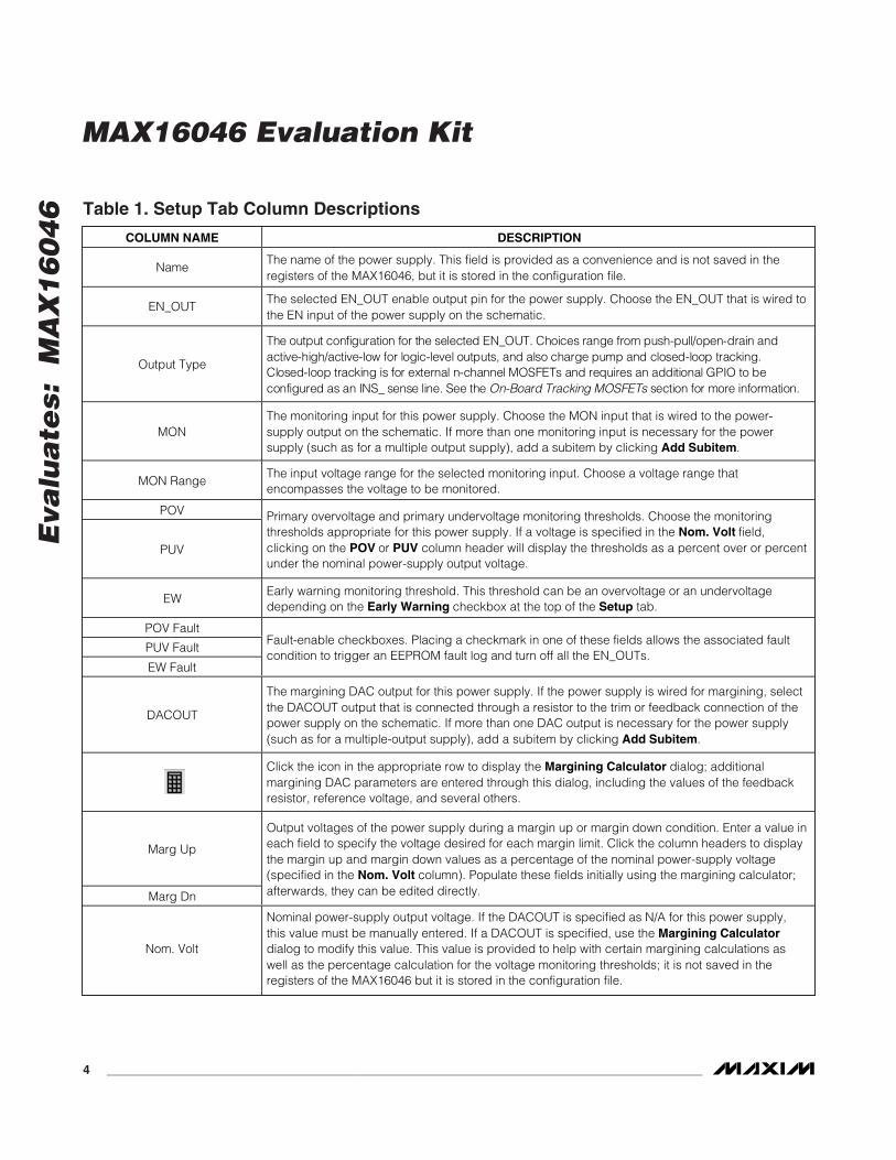
Table 1. Setup Tab Column Descriptions
COLUMN NAME DESCRIPTION
NameThe name of the power supply. This field is provided as a convenience and is not saved in theregisters of the MAX16046, but it is stored in the configuration file.
EN_OUTThe selected EN_OUT enable output pin for the power supply. Choose the EN_OUT that is wired tothe EN input of the power supply on the schematic.
Output Type
The outp ut confi g ur ati on for the sel ected E N _O U T. C hoi ces r ang e fr om p ush- p ul l /op en- d r ai n and acti ve- hi g h/acti ve- l ow for l og i c- l evel outp uts, and al so char g e p um p and cl osed - l oop tr acki ng .C l osed - l oop tr acki ng i s for exter nal n- channel M OS FE Ts and r eq ui r es an ad d i ti onal G P IO to b econfi g ur ed as an IN S _ sense l i ne. S ee the O n- Boar d Tr acki ng M OS FE Ts secti on for m or e i nfor m ati on.
MONThe monitoring input for this power supply. Choose the MON input that is wired to the power-supply output on the schematic. If more than one monitoring input is necessary for the powersupply (such as for a multiple output supply), add a subitem by clicking Add Subitem.
MON RangeThe input voltage range for the selected monitoring input. Choose a voltage range thatencompasses the voltage to be monitored.
POV
PUV
Primary overvoltage and primary undervoltage monitoring thresholds. Choose the monitoringthresholds appropriate for this power supply. If a voltage is specified in the Nom. Volt field,clicking on the POV or PUV column header will display the thresholds as a percent over or percentunder the nominal power-supply output voltage.
EWEarly warning monitoring threshold. This threshold can be an overvoltage or an undervoltagedepending on the Early Warning checkbox at the top of the Setup tab.
POV Fault
PUV Fault
EW Fault
Fault-enable checkboxes. Placing a checkmark in one of these fields allows the associated faultcondition to trigger an EEPROM fault log and turn off all the EN_OUTs.
DACOUT
The margining DAC output for this power supply. If the power supply is wired for margining, selectthe DACOUT output that is connected through a resistor to the trim or feedback connection of thepower supply on the schematic. If more than one DAC output is necessary for the power supply(such as for a multiple-output supply), add a subitem by clicking Add Subitem.
Click the icon in the appropriate row to display the Margining Calculator dialog; additionalmargining DAC parameters are entered through this dialog, including the values of the feedbackresistor, reference voltage, and several others.
Marg Up
Marg Dn
Output voltages of the power supply during a margin up or margin down condition. Enter a value ineach field to specify the voltage desired for each margin limit. Click the column headers to displaythe margin up and margin down values as a percentage of the nominal power-supply voltage(specified in the Nom. Volt column). Populate these fields initially using the margining calculator;afterwards, they can be edited directly.
Nom. Volt
Nominal power-supply output voltage. If the DACOUT is specified as N/A for this power supply,this value must be manually entered. If a DACOUT is specified, use the Margining Calculatordialog to modify this value. This value is provided to help with certain margining calculations aswell as the percentage calculation for the voltage monitoring thresholds; it is not saved in theregisters of the MAX16046 but it is stored in the configuration file.
Eva
lua
tes: M
AX
16
04
6
To add a power supply to the list, click Add Item. Toadd an additional monitoring input or margining DACoutput to a power supply, as in the case of a multiple-output power supply, select the row representing thepower supply and click Add Subitem. To remove apower supply or additional monitoring input/marginingDAC output, select the row to be removed and clickDelete Item. To remove all the power supplies, clickClear Tree.
The early warning thresholds (EW) can be configuredas overvoltage thresholds or undervoltage thresholds.Click Undervoltage or Overvoltage as desired.
The contents of the Setup tab are not sent to the regis-ters of the MAX16046 until the Write To Registers but-ton is clicked. After making a change, click Write ToRegisters to update the device registers.
Margining CalculatorTo facilitate resistor value calculation for designs usingthe margining DACs, the EV kit software provides amargining calculator. Access the margining calculatorby clicking the icon for the desired DACOUT chan-nel in the Setup tab.
Figure 3 shows the Margining Calculator dialog. Thisprovides a convenient interface to the margining calcu-lations listed in the Applications Information section ofthe MAX16046 data sheet.
To use the margining calculator, select the desired for-mulas using the Connection Style option buttons. Thediagram on the left will update to reflect the wiring forthat particular style. Enter the reference voltage usedby the power supply under Reference Voltage (Vref),and select the DAC Range so the reference voltage isapproximately in the middle of the range. For the feed-
MAX16046 Evaluation Kit
_______________________________________________________________________________________ 5
Figure 3. Margining Calculator

Eva
lua
tes:
M
AX
16
04
6
MAX16046 Evaluation Kit
6 _______________________________________________________________________________________
back pin style, Nominal VOUT is automatically calcu-lated based on R1 and R2. For the trim pin style, enterthe nominal output voltage. The Nominal VOUT valueis identical to that of the field in the Setup tab, and canbe changed from both places when the trim pin style isselected. Enter the three resistor values, R1 Value(k),R2 Value(k), R3 Value(k).
After these values have been entered, values under theVOUT Voltage, % of Nominal, and Register Valuecolumns update automatically. Rows Output (DAC=0)and Output (DAC=255) indicate the maximum and min-imum limits of the output voltage, both as voltages andas percentages of the nominal output voltage.
Fields in the last two rows can each be modified manu-ally, and the remaining fields in the same row will auto-matically be recalculated. For example, if a percentage
is entered in the % of Nominal field of the Margin UpSetting row, the VOUT Voltage and Register Value forthat row will be recalculated. Decimal values in theRegister Value column are actual 8-bit DAC codesloaded into the MAX16046 registers. Values in the % ofNominal and VOUT Voltage fields are identical tothose shown in the appropriate fields of the Setup taband can be changed from both places.
Click Ok to save the changes to the Setup tab. ClickCancel and any changes will be lost. Changes will notbe saved to the registers of the MAX16046 until WriteTo Registers (on the Setup tab) is clicked.
Table 2 provides the margining settings for LDO1 andLDO2 on the MAX16046 EV kit.
Table 2. Margining Settings
SETTINGCONNECTION
STYLEREFERENCE
VOLTAGEDAC RANGE
(V)R1 VALUE(k) R2 VALUE(k) R3 VALUE(k)
LDO1 (DACOUT2) Feedback Pin 1.21 0.8 to 1.6 133 78.7 78.7
LDO2 (DACOUT3) Feedback Pin 1.21 0.8 to 1.6 84.5 78.7 66.5
Eva
lua
tes: M
AX
16
04
6
MAX16046 Evaluation Kit
_______________________________________________________________________________________ 7
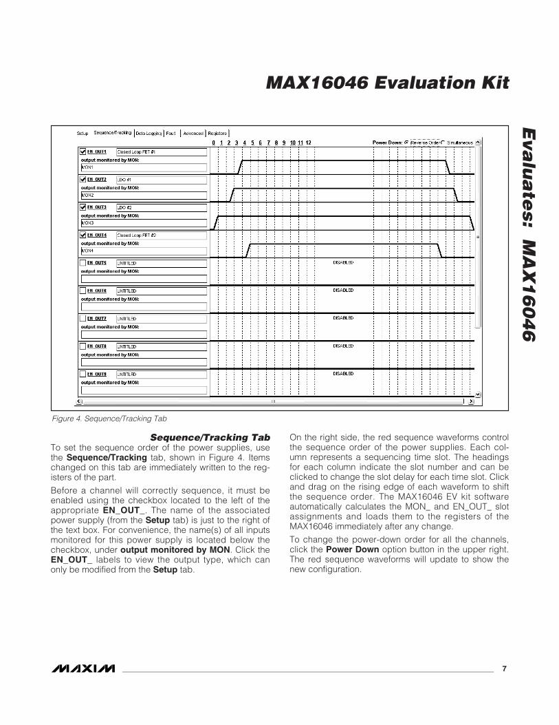
Sequence/Tracking TabTo set the sequence order of the power supplies, usethe Sequence/Tracking tab, shown in Figure 4. Itemschanged on this tab are immediately written to the reg-isters of the part.
Before a channel will correctly sequence, it must beenabled using the checkbox located to the left of theappropriate EN_OUT_. The name of the associatedpower supply (from the Setup tab) is just to the right ofthe text box. For convenience, the name(s) of all inputsmonitored for this power supply is located below thecheckbox, under output monitored by MON. Click theEN_OUT_ labels to view the output type, which canonly be modified from the Setup tab.
On the right side, the red sequence waveforms controlthe sequence order of the power supplies. Each col-umn represents a sequencing time slot. The headingsfor each column indicate the slot number and can beclicked to change the slot delay for each time slot. Clickand drag on the rising edge of each waveform to shiftthe sequence order. The MAX16046 EV kit softwareautomatically calculates the MON_ and EN_OUT_ slotassignments and loads them to the registers of theMAX16046 immediately after any change.
To change the power-down order for all the channels,click the Power Down option button in the upper right.The red sequence waveforms will update to show thenew configuration.
Figure 4. Sequence/Tracking Tab
Eva
lua
tes:
M
AX
16
04
6
MAX16046 Evaluation Kit
8 _______________________________________________________________________________________
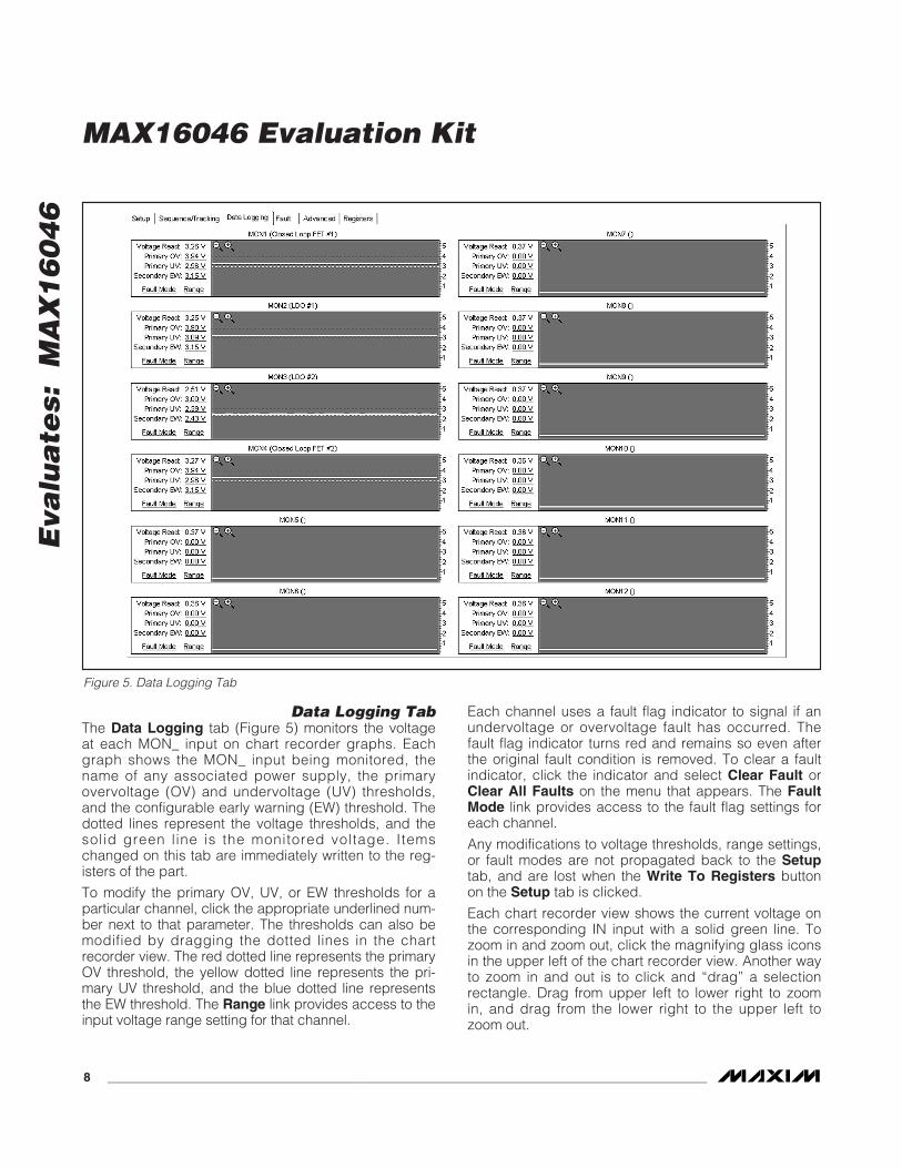
Data Logging TabThe Data Logging tab (Figure 5) monitors the voltageat each MON_ input on chart recorder graphs. Eachgraph shows the MON_ input being monitored, thename of any associated power supply, the primaryovervoltage (OV) and undervoltage (UV) thresholds,and the configurable early warning (EW) threshold. Thedotted lines represent the voltage thresholds, and thesolid green line is the monitored voltage. Itemschanged on this tab are immediately written to the reg-isters of the part.
To modify the primary OV, UV, or EW thresholds for aparticular channel, click the appropriate underlined num-ber next to that parameter. The thresholds can also bemodified by dragging the dotted lines in the chartrecorder view. The red dotted line represents the primaryOV threshold, the yellow dotted line represents the pri-mary UV threshold, and the blue dotted line representsthe EW threshold. The Range link provides access to theinput voltage range setting for that channel.
Each channel uses a fault flag indicator to signal if anundervoltage or overvoltage fault has occurred. Thefault flag indicator turns red and remains so even afterthe original fault condition is removed. To clear a faultindicator, click the indicator and select Clear Fault orClear All Faults on the menu that appears. The FaultMode link provides access to the fault flag settings foreach channel.
Any modifications to voltage thresholds, range settings,or fault modes are not propagated back to the Setuptab, and are lost when the Write To Registers buttonon the Setup tab is clicked.
Each chart recorder view shows the current voltage onthe corresponding IN input with a solid green line. Tozoom in and zoom out, click the magnifying glass iconsin the upper left of the chart recorder view. Another wayto zoom in and out is to click and “drag” a selectionrectangle. Drag from upper left to lower right to zoomin, and drag from the lower right to the upper left tozoom out.
Figure 5. Data Logging Tab
Eva
lua
tes: M
AX
16
04
6
MAX16046 Evaluation Kit
_______________________________________________________________________________________ 9
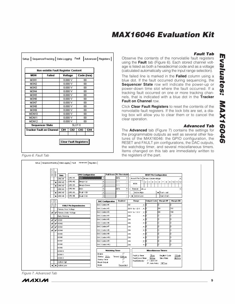
Fault TabObserve the contents of the nonvolatile fault registersusing the Fault tab (Figure 6). Each stored channel volt-age is listed as both a hexadecimal code and as a voltage(calculated automatically using the input range selection).
The failed line is marked in the Failed column using ablue dot. If the fault occurred during sequencing, theSequencer State row will indicate the power-up orpower-down time slot where the fault occurred. If atracking fault occurred on one or more tracking chan-nels, that is indicated with a blue dot in the TrackerFault on Channel row.
Click Clear Fault Registers to reset the contents of thenonvolatile fault registers. If the lock bits are set, a dia-log box will allow you to clear them or to cancel theclear operation.
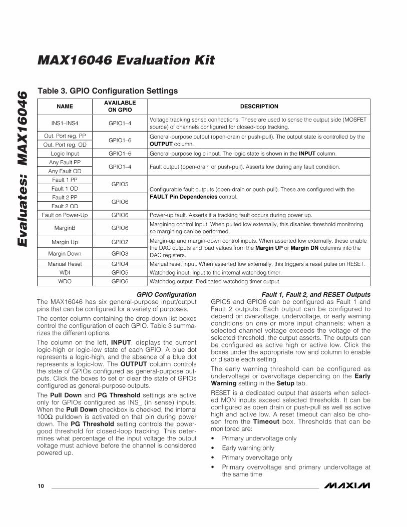
Advanced TabThe Advanced tab (Figure 7) contains the settings forthe programmable outputs as well as several other fea-tures of the MAX16046: the GPIO configuration, theRESET and FAULT pin configurations, the DAC outputs,the watchdog timer, and several miscellaneous timers.Items changed on this tab are immediately written tothe registers of the part.Figure 6. Fault Tab
Figure 7. Advanced Tab
Eva
lua
tes:
M
AX
16
04
6
MAX16046 Evaluation Kit
10 ______________________________________________________________________________________
GPIO ConfigurationThe MAX16046 has six general-purpose input/outputpins that can be configured for a variety of purposes.
The center column containing the drop-down list boxescontrol the configuration of each GPIO. Table 3 summa-rizes the different options.
The column on the left, INPUT, displays the currentlogic-high or logic-low state of each GPIO. A blue dotrepresents a logic-high, and the absence of a blue dotrepresents a logic-low. The OUTPUT column controlsthe state of GPIOs configured as general-purpose out-puts. Click the boxes to set or clear the state of GPIOsconfigured as general-purpose outputs.
The Pull Down and PG Threshold settings are activeonly for GPIOs configured as INS_ (in sense) inputs.When the Pull Down checkbox is checked, the internal100Ω pulldown is activated on that pin during powerdown. The PG Threshold setting controls the power-good threshold for closed-loop tracking. This deter-mines what percentage of the input voltage the outputvoltage must achieve before the channel is consideredpowered up.
Fault 1, Fault 2, and RESET OutputsGPIO5 and GPIO6 can be configured as Fault 1 andFault 2 outputs. Each output can be configured todepend on overvoltage, undervoltage, or early warningconditions on one or more input channels; when aselected channel voltage exceeds the voltage of theselected threshold, the output asserts. The outputs canbe configured as active high or active low. Click theboxes under the appropriate row and column to enableor disable each setting.
The early warning threshold can be configured asundervoltage or overvoltage depending on the EarlyWarning setting in the Setup tab.
RESET is a dedicated output that asserts when select-ed MON inputs exceed selected thresholds. It can beconfigured as open drain or push-pull as well as activehigh and active low. A reset timeout can also be cho-sen from the Timeout box. Thresholds that can bemonitored are:
• Primary undervoltage only
• Early warning only
• Primary overvoltage only
• Primary overvoltage and primary undervoltage atthe same time
Table 3. GPIO Configuration Settings
NAMEAVAILABLE
ON GPIODESCRIPTION
INS1–INS4 GPIO1–4Voltage tracking sense connections. These are used to sense the output side (MOSFETsource) of channels configured for closed-loop tracking.
Out. Port reg. PP
Out. Port reg. ODGPIO1–6
General-purpose output (open-drain or push-pull). The output state is controlled by theOUTPUT column.
Logic Input GPIO1–6 General-purpose logic input. The logic state is shown in the INPUT column.
Any Fault PP
Any Fault ODGPIO1–4 Fault output (open-drain or push-pull). Asserts low during any fault condition.
Fault 1 PP
Fault 1 ODGPIO5
Fault 2 PP
Fault 2 ODGPIO6
Configurable fault outputs (open-drain or push-pull). These are configured with theFAULT Pin Dependencies control.
Fault on Power-Up GPIO6 Power-up fault. Asserts if a tracking fault occurs during power up.
MarginB GPIO6Margining control input. When pulled low externally, this disables threshold monitoringso margining can be performed.
Margin Up GPIO2
Margin Down GPIO3
Margin-up and margin-down control inputs. When asserted low externally, these enablethe DAC outputs and load values from the Margin UP or Margin DN columns into theDAC registers.
Manual Reset GPIO4 Manual reset input. When asserted low externally, this triggers a reset pulse on RESET.
WDI GPIO5 Watchdog input. Input to the internal watchdog timer.
WDO GPIO6 Watchdog output. Dedicated watchdog timer output.

DAC ConfigurationThe preferred method for configuring the marginingDACs is through the Setup tab, but the DAC outputscan also be configured from the Advanced tab. Clickthe Enabled checkbox to turn a DAC on or off. For aDAC output to turn on, both the Enabled checkboxmust be checked and the Range selection must be oneof 0.4V to 0.8V, 0.6V to 1.2V, or 0.8V to 1.6V.
To set the DAC output voltage, enter a decimal numberfrom 0 to 255 in the Output Code box. The new value willbe written to the appropriate register and the DAC outputwill update immediately. The Margin UP and Margin DNboxes contain the decimal codes placed at all DAC out-puts when the margin-up or margin-down inputs areasserted (see the GPIO Configuration section).
Any modifications to the DAC settings are not propa-gated back to the Setup tab, and are lost when theWrite To Registers button on the Setup tab is clicked.
Watchdog Timer ConfigurationThe internal watchdog timer can be configured in thisbox. Check the Enable checkbox to turn on the watch-dog timer. Click the blue link next to Timeout to changethe watchdog timeout period.
If the watchdog timeout period needs to be extendedduring initial startup to allow for an external micro-processor to complete a boot-up sequence, check theStartup Timer checkbox and specify the startup time-out with the blue link next to Startup.
Normally, the watchdog timer asserts WDO (if GPIO6 isconfigured appropriately), but if desired, the watchdog
timer can also assert RESET. Check the Reset Outputcheckbox to enable this behavior.
If Mode is set to Dependent, the watchdog timer turnson after power sequencing is complete and RESETdeasserts. If Mode is set to Independent, the watch-dog timer turns on immediately and remains on regard-less of the power sequencing state.
Miscellaneous TimersThe Fault Up Timer controls the period of time allowedfor a power supply to fall within its power-good thresh-olds from when it is turned on. Conversely, the FaultDown Timer setting controls the period allowed for apower-supply rail to turn off.
During a fault condition, the MAX16046 can either shutoff or try to sequence again, depending on the FaultBehavior setting. Select Latch-Off to have theMAX16046 shut down and not attempt to restart powersequencing. Select Auto-Retry and select a delay peri-od to have the MAX16046 attempt sequencing againafter the delay occurs.
When a monitored voltage falls outside one of the pro-grammable thresholds, the MAX16046’s internal ADCwill repeat several conversions on the same channel.To trigger a fault condition, the voltage must remainoutside the threshold for a certain number of conver-sions. This number is controlled by the Deglitch Cyclesetting. Allowable options are: 2, 4, 8, and 16 cycles.
The Slew Rate setting controls the tracking slew ratefor channels configured in closed-loop tracking mode.
Eva
lua
tes: M
AX
16
04
6
MAX16046 Evaluation Kit
______________________________________________________________________________________ 11
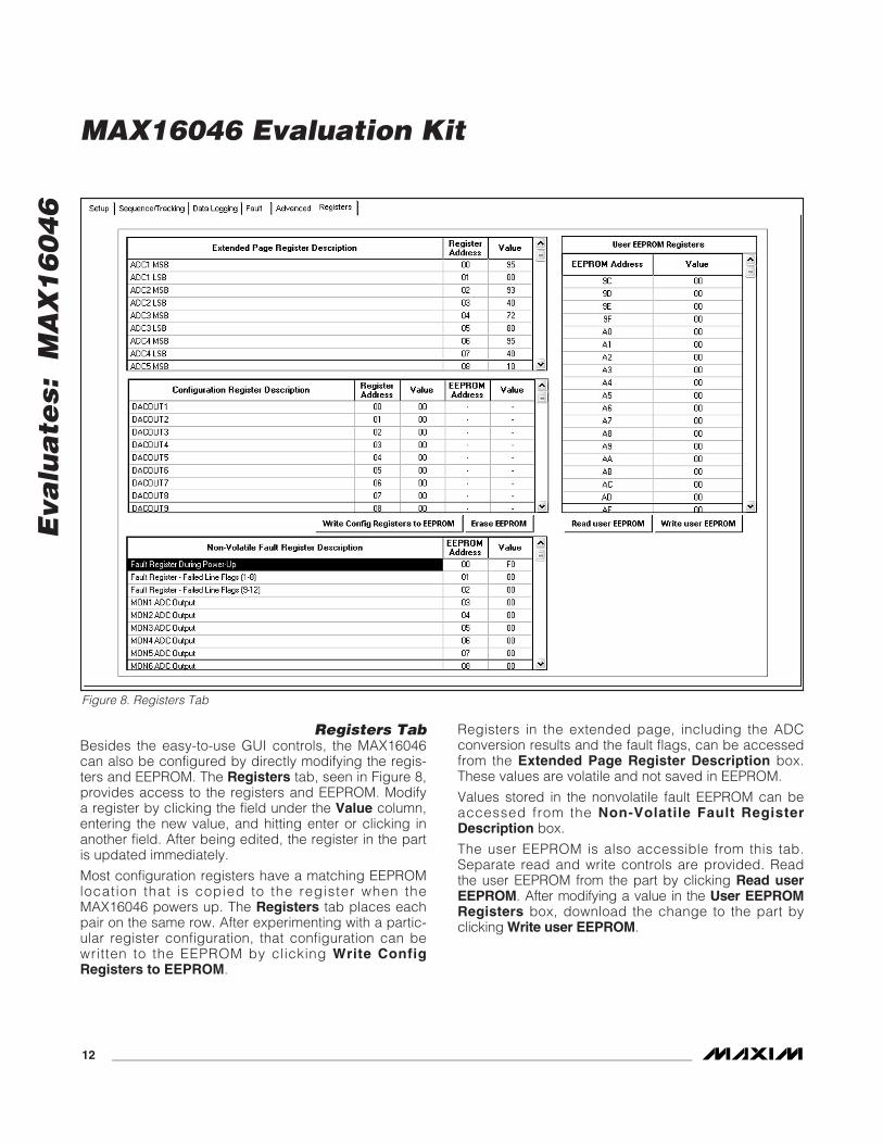
Registers TabBesides the easy-to-use GUI controls, the MAX16046can also be configured by directly modifying the regis-ters and EEPROM. The Registers tab, seen in Figure 8,provides access to the registers and EEPROM. Modifya register by clicking the field under the Value column,entering the new value, and hitting enter or clicking inanother field. After being edited, the register in the partis updated immediately.
Most configuration registers have a matching EEPROMlocation that is copied to the register when theMAX16046 powers up. The Registers tab places eachpair on the same row. After experimenting with a partic-ular register configuration, that configuration can bewritten to the EEPROM by clicking Write ConfigRegisters to EEPROM.
Registers in the extended page, including the ADCconversion results and the fault flags, can be accessedfrom the Extended Page Register Description box.These values are volatile and not saved in EEPROM.
Values stored in the nonvolatile fault EEPROM can beaccessed from the Non-Volatile Fault RegisterDescription box.
The user EEPROM is also accessible from this tab.Separate read and write controls are provided. Readthe user EEPROM from the part by clicking Read userEEPROM. After modifying a value in the User EEPROMRegisters box, download the change to the part byclicking Write user EEPROM.
Eva
lua
tes:
M
AX
16
04
6
MAX16046 Evaluation Kit
12 ______________________________________________________________________________________
Figure 8. Registers Tab
Menu ReferenceFile
Open Configuration and Save Configuration As loadand save the contents of the setup tab (which are notsaved to the MAX16046 registers), as well as the com-plete register contents to a standard XML file. Tip: XMLfiles can be viewed in an indented, color-coded formatin many web browsers.
Save as SVF writes the EEPROM configuration to anSVF file, which is a standard format used by JTAGdevice programmers for production programming.
SystemConnect… directs the software to open a connectionwith a connected EV kit, and displays the Connect dia-log (Figure 1) to select the connection type. Once con-nected, this menu item changes to Disconnect.
Fault Control changes the amount of information thatthe MAX16046 saves during a nonvolatile fault saveevent. This writes to register r47h.
Send REBOOT sends the reboot command to theMAX16046, which will then reload the configurationEEPROM into the configuration registers.
Trigger FAULT Save manually triggers a nonvolatilefault save event.
Save Configuration to EEPROM writes the contents ofthe configuration registers to the EEPROM.
Configuration Register Lock controls and displays thestatus of the register and configuration EEPROM lockbit, located in register r5Dh. The registers and the con-figuration EEPROM can be locked with this setting to
prevent unintentional modification of configuration set-tings. The lock icon on the status bar also indicatesand controls this lock bit.
Non-Volatile EEPROM Lock controls and displays thestatus of the nonvolatile EEPROM lock bit, located inregister r5Dh. The fault EEPROM is locked automaticallywhen a fault condition occurs, and it must be unlockedbefore any subsequent fault will get stored to EEPROM.A check mark will appear next to this item when theEEPROM is locked. Clear it by selecting the menu item.
Software Enable controls the MAX16046’s sequencer.Click this menu item to enable or disable the MAX16046.A check mark appears next to this menu item whenenabled. For power-up sequencing to occur, this menuitem must be checked and the hardware enable switchon the MAX16046 EV kit must be switched on.
DeviceThis menu selects the target device. The EV kit uses theMAX16046 by default, but the EV kit software can alsogenerate configuration files for and program theMAX16047/MAX16048/MAX16049.
PollingOn and Off turn register polling on and off. Whenpolling is on, the controls in all the tabs are periodicallyrefreshed from the physical registers. If polling is off,register contents can be read from the device byselecting Read All Registers.
HelpAbout launches the About dialog, which displays thesoftware version and, if the EV kit is connected, thefirmware revision of the USB interface.
Eva
lua
tes: M
AX
16
04
6
MAX16046 Evaluation Kit
______________________________________________________________________________________ 13
Eva
lua
tes:
M
AX
16
04
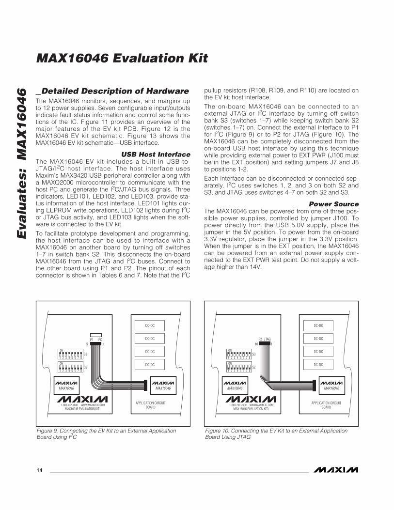
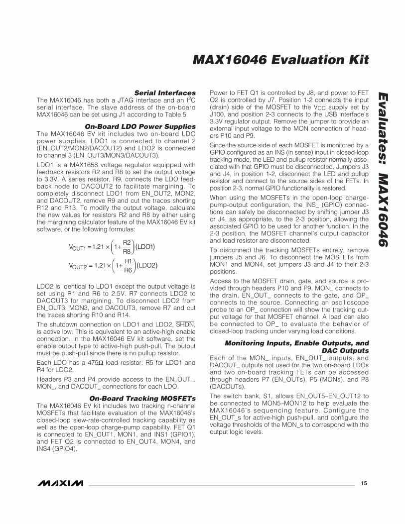
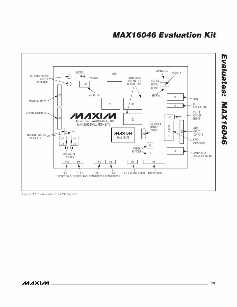
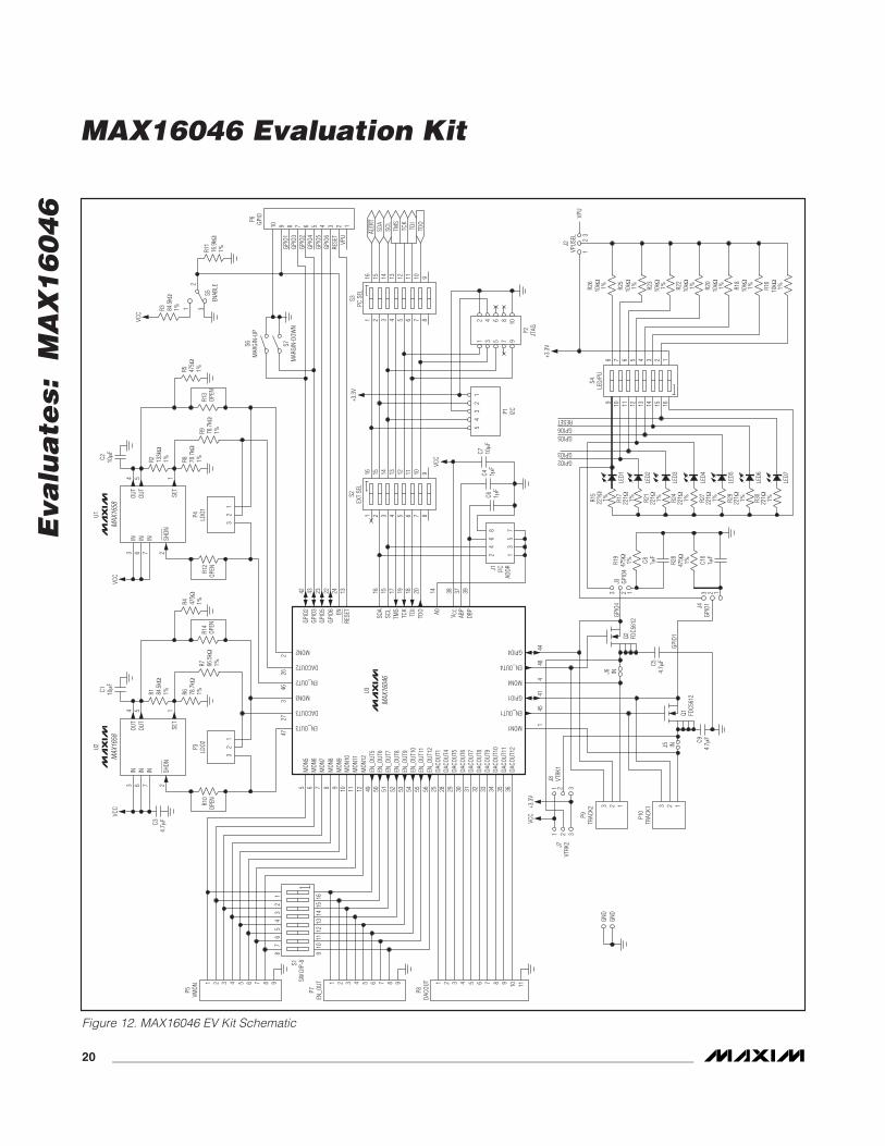
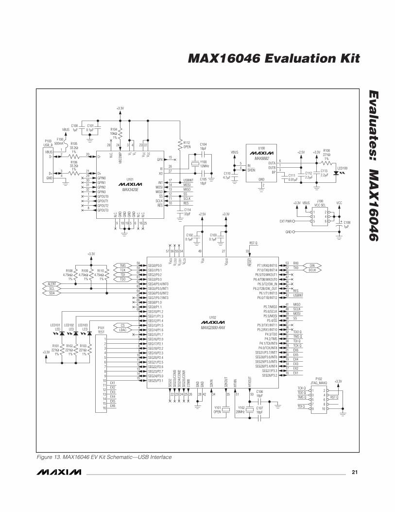
6 Detailed Description of HardwareThe MAX16046 monitors, sequences, and margins upto 12 power supplies. Seven configurable input/outputsindicate fault status information and control some func-tions of the IC. Figure 11 provides an overview of themajor features of the EV kit PCB. Figure 12 is theMAX16046 EV kit schematic. Figure 13 shows theMAX16046 EV kit schematic—USB interface.
USB Host InterfaceThe MAX16046 EV kit includes a built-in USB-to-JTAG/I2C host interface. The host interface usesMaxim’s MAX3420 USB peripheral controller along witha MAXQ2000 microcontroller to communicate with thehost PC and generate the I2C/JTAG bus signals. Threeindicators, LED101, LED102, and LED103, provide sta-tus information of the host interface. LED101 lights dur-ing EEPROM write operations, LED102 lights during I2Cor JTAG bus activity, and LED103 lights when the soft-ware is connected to the EV kit.
To facilitate prototype development and programming,the host interface can be used to interface with aMAX16046 on another board by turning off switches1–7 in switch bank S2. This disconnects the on-boardMAX16046 from the JTAG and I2C buses. Connect tothe other board using P1 and P2. The pinout of eachconnector is shown in Tables 6 and 7. Note that the I2C
pullup resistors (R108, R109, and R110) are located onthe EV kit host interface.
The on-board MAX16046 can be connected to anexternal JTAG or I2C interface by turning off switchbank S3 (switches 1–7) while keeping switch bank S2(switches 1–7) on. Connect the external interface to P1for I2C (Figure 9) or to P2 for JTAG (Figure 10). TheMAX16046 can be completely disconnected from theon-board USB host interface by using this techniquewhile providing external power to EXT PWR (J100 mustbe in the EXT position) and setting jumpers J7 and J8to positions 1-2.
Each interface can be disconnected or connected sep-arately. I2C uses switches 1, 2, and 3 on both S2 andS3, and JTAG uses switches 4–7 on both S2 and S3.
Power SourceThe MAX16046 can be powered from one of three pos-sible power supplies, controlled by jumper J100. Topower directly from the USB 5.0V supply, place thejumper in the 5V position. To power from the on-board3.3V regulator, place the jumper in the 3.3V position.When the jumper is in the EXT position, the MAX16046can be powered from an external power supply con-nected to the EXT PWR test point. Do not supply a volt-age higher than 14V.
MAX16046 Evaluation Kit
14 ______________________________________________________________________________________
1-800-737-7600 WWW.MAXIM-IC.COMMAX16046 EVALUATION KIT+
MAX16046 MAX16046
1
ON
ON
2 3 4 5 6 7 8S3
S2
10P2 JTAG
DC-DC
DC-DC
DC-DC
DC-DC
1
APPLICATION CIRCUITBOARD
1 2 3 4 5 6 7 8
Figure 10. Connecting the EV Kit to an External ApplicationBoard Using JTAG
Figure 9. Connecting the EV Kit to an External ApplicationBoard Using I2C
1-800-737-7600 WWW.MAXIM-IC.COMMAX16046 EVALUATION KIT+
MAX16046 MAX16046
1
ON
ON
2 3 4 5 6 7 8S3
S2
5P1 I2C
DC-DC
DC-DC
DC-DC
DC-DC
1
APPLICATION CIRCUITBOARD
1 2 3 4 5 6 7 8
Serial InterfacesThe MAX16046 has both a JTAG interface and an I2Cserial interface. The slave address of the on-boardMAX16046 can be set using J1 according to Table 5.
On-Board LDO Power SuppliesThe MAX16046 EV kit includes two on-board LDOpower supplies. LDO1 is connected to channel 2(EN_OUT2/MON2/DACOUT2) and LDO2 is connectedto channel 3 (EN_OUT3/MON3/DACOUT3).
LDO1 is a MAX1658 voltage regulator equipped withfeedback resistors R2 and R8 to set the output voltageto 3.3V. A series resistor, R9, connects the LDO feed-back node to DACOUT2 to facilitate margining. Tocompletely disconnect LDO1 from EN_OUT2, MON2,and DACOUT2, remove R9 and cut the traces shortingR12 and R13. To modify the output voltage, calculatethe new values for resistors R2 and R8 by either usingthe margining calculator feature of the MAX16046 EV kitsoftware, or the following formulas:
LDO2 is identical to LDO1 except the output voltage isset using R1 and R6 to 2.5V. R7 connects LDO2 toDACOUT3 for margining. To disconnect LDO2 fromEN_OUT3, MON3, and DACOUT3, remove R7 and cutthe traces shorting R10 and R14.
The shutdown connection on LDO1 and LDO2, SHDN,is active low. This is equivalent to an active-high enableconnection. In the MAX16046 EV kit software, set theenable output type to active-high push-pull. The outputmust be push-pull since there is no pullup resistor.
Each LDO has a 475Ω load resistor: R5 for LDO1 andR4 for LDO2.
Headers P3 and P4 provide access to the EN_OUT_,MON_, and DACOUT_ connections for each LDO.
On-Board Tracking MOSFETsThe MAX16046 EV kit includes two tracking n-channelMOSFETs that facilitate evaluation of the MAX16046’sclosed-loop slew-rate-controlled tracking capability aswell as the open-loop charge-pump capability. FET Q1is connected to EN_OUT1, MON1, and INS1 (GPIO1),and FET Q2 is connected to EN_OUT4, MON4, andINS4 (GPIO4).
Power to FET Q1 is controlled by J8, and power to FETQ2 is controlled by J7. Position 1-2 connects the input(drain) side of the MOSFET to the VCC supply set byJ100, and position 2-3 connects to the USB interface’s3.3V regulator output. Remove the jumper to provide anexternal input voltage to the MON connection of head-ers P10 and P9.
Since the source side of each MOSFET is monitored by aGPIO configured as an INS (in sense) input in closed-looptracking mode, the LED and pullup resistor normally asso-ciated with that GPIO must be disconnected. Jumpers J3and J4, in position 1-2, disconnect the LED and pullupresistor and connect to the source sides of the FETs. Inposition 2-3, normal GPIO functionality is restored.
When using the MOSFETs in the open-loop charge-pump-output configuration, the INS_ (GPIO) connec-tions can safely be disconnected by shifting jumper J3or J4, as appropriate, to the 2-3 position, allowing theassociated GPIO to be used for another function. In the2-3 position, the MOSFET channel’s output capacitorand load resistor are disconnected.
To disconnect the tracking MOSFETs entirely, removejumpers J5 and J6. To disconnect the MOSFETs fromMON1 and MON4, set jumpers J3 and J4 to their 2-3positions.
Access to the MOSFET drain, gate, and source is pro-vided through headers P10 and P9. MON_ connects tothe drain, EN_OUT_ connects to the gate, and OP_connects to the source. Connecting an oscilloscopeprobe to an OP_ connection will show the tracking out-put voltage for that MOSFET channel. A load can alsobe connected to OP_ to evaluate the behavior ofclosed-loop tracking under varying load conditions.
Monitoring Inputs, Enable Outputs, andDAC Outputs
Each of the MON_ inputs, EN_OUT_ outputs, andDACOUT_ outputs not used for the two on-board LDOsand two on-board tracking FETs can be accessedthrough headers P7 (EN_OUTs), P5 (MONs), and P8(DACOUTs).
The switch bank, S1, allows EN_OUT5–EN_OUT12 tobe connected to MON5–MON12 to help evaluate theMAX16046’s sequencing feature. Configure theEN_OUT_s for active-high push-pull, and configure thevoltage thresholds of the MON_s to correspond with theoutput logic levels.
VRR
LDO
V
OUT
OUT
1
2
1 21 128
1
1
.= × +⎛⎝⎜
⎞⎠⎟ ( )
= ..21 116
2× +⎛⎝⎜
⎞⎠⎟ ( )R
RLDO
Eva
lua
tes: M
AX
16
04
6
MAX16046 Evaluation Kit
______________________________________________________________________________________ 15
Eva
lua
tes:
M
AX
16
04
6 General-Purpose Inputs and OutputsEach GPIO has a separate indicator LED and pullupresistor, and each signal is brought out to a pin on P6.An LED will light to indicate that the associated outputhas gone to the logic-low state. The LEDs can be dis-abled by turning off switch 1 in switch bank S4. Thepullup resistors are individually switched by S4; seeTable 4 for the assignments of each switch in the switchbank. To use an external pullup voltage, connect J2 inthe 2-3 position and connect the voltage source to theVPU pin of P6.
Margin Up and Margin DownThrough the MAX16046 EV kit software, GPIO2 andGPIO3 can be configured as margin-up and margin-down inputs, respectively. Switches S6 and S7 pullGPIO2 and GPIO3 to ground. It is not necessary to dis-able the LEDs or disconnect the pullup resistors forGPIO2 or GPIO3 to use this function.
Hardware EnableThe MAX16046 has an analog EN connection that canbe used to trigger power-up or power-down sequenc-ing. An on-board resistive divider formed by R3 andR11 set the falling threshold to 3.0V on VCC; the thresh-old can be modified by changing R3 and R11 according to the following formulas:
EN can be manually controlled using the hardwareenable switch, S5. Set S5 to the OFF position to pull ENto 0V, and set S5 to the ON position to allow EN torespond to the VCC voltage.
MarginingTwo of the MAX16046’s DACOUTs (DACOUT2 andDACOUT3) connect to the two LDO regulators on theEV kit, LDO1 and LDO2, respectively. The rest go toheader P8. To evaluate the margining capabilities of theMAX16046, configure GPIO2 and GPIO3 as margin-upand margin-down inputs from the Advanced tab in theEV kit software. When the margin-down (S7) or margin-up (S6) pushbuttons are pressed, the DAC outputs areenabled and the DAC codes are loaded from theMargin UP or Margin DN columns in the Advancedtab, causing the LDO regulator output voltages to shift.
VRR
V
VCC TH RISING
VCC
_ _
_
.= × +⎛⎝⎜
⎞⎠⎟
0 525 1311
TTH FALLINGRR_ .= × +⎛
⎝⎜⎞⎠⎟
0 500 1311
MAX16046 Evaluation Kit
16 ______________________________________________________________________________________
Eva
lua
tes: M
AX
16
04
6
MAX16046 Evaluation Kit
______________________________________________________________________________________ 17
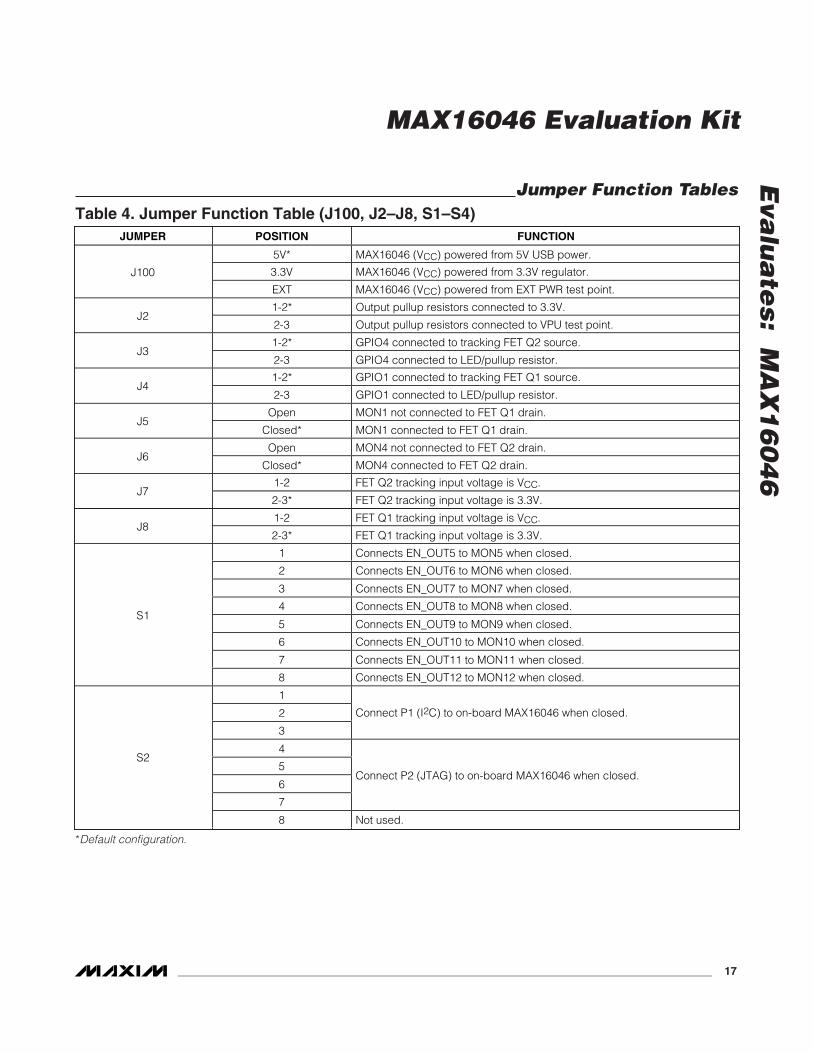
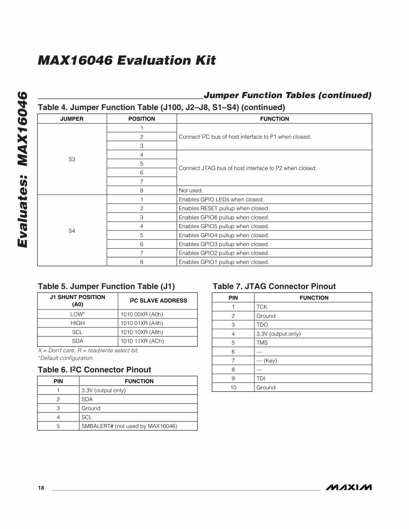
Jumper Function Tables
JUMPER POSITION FUNCTION
5V* MAX16046 (VCC) powered from 5V USB power.
3.3V MAX16046 (VCC) powered from 3.3V regulator.J100
EXT MAX16046 (VCC) powered from EXT PWR test point.
1-2* Output pullup resistors connected to 3.3V.J2
2-3 Output pullup resistors connected to VPU test point.
1-2* GPIO4 connected to tracking FET Q2 source.J3
2-3 GPIO4 connected to LED/pullup resistor.
1-2* GPIO1 connected to tracking FET Q1 source.J4
2-3 GPIO1 connected to LED/pullup resistor.
Open MON1 not connected to FET Q1 drain.J5
Closed* MON1 connected to FET Q1 drain.
Open MON4 not connected to FET Q2 drain.J6
Closed* MON4 connected to FET Q2 drain.
1-2 FET Q2 tracking input voltage is VCC.J7
2-3* FET Q2 tracking input voltage is 3.3V.
1-2 FET Q1 tracking input voltage is VCC.J8
2-3* FET Q1 tracking input voltage is 3.3V.
1 Connects EN_OUT5 to MON5 when closed.
2 Connects EN_OUT6 to MON6 when closed.
3 Connects EN_OUT7 to MON7 when closed.
4 Connects EN_OUT8 to MON8 when closed.
5 Connects EN_OUT9 to MON9 when closed.
6 Connects EN_OUT10 to MON10 when closed.
7 Connects EN_OUT11 to MON11 when closed.
S1
8 Connects EN_OUT12 to MON12 when closed.
1
2
3
Connect P1 (I2C) to on-board MAX16046 when closed.
4
5
6
7
Connect P2 (JTAG) to on-board MAX16046 when closed.
S2
8 Not used.
Table 4. Jumper Function Table (J100, J2–J8, S1–S4)
*Default configuration.
Eva
lua
tes:
M
AX
16
04
6
MAX16046 Evaluation Kit
18 ______________________________________________________________________________________
Jumper Function Tables (continued)
JUMPER POSITION FUNCTION
1
2
3
Connect I2C bus of host interface to P1 when closed.
4
5
6
7
Connect JTAG bus of host interface to P2 when closed.
S3
8 Not used.
1 Enables GPIO LEDs when closed.
2 Enables RESET pullup when closed.
3 Enables GPIO6 pullup when closed.
4 Enables GPIO5 pullup when closed.
5 Enables GPIO4 pullup when closed.
6 Enables GPIO3 pullup when closed.
7 Enables GPIO2 pullup when closed.
S4
8 Enables GPIO1 pullup when closed.
Table 4. Jumper Function Table (J100, J2–J8, S1–S4) (continued)
J1 SHUNT POSITION(A0)
I2C SLAVE ADDRESS
LOW* 1010 00XR (A0h)
HIGH 1010 01XR (A4h)
SCL 1010 10XR (A8h)
SDA 1010 11XR (ACh)
Table 5. Jumper Function Table (J1)PIN FUNCTION
1 TCK
2 Ground
3 TDO
4 3.3V (output only)
5 TMS
6 —
7 — (Key)
8 —
9 TDI
10 Ground
Table 7. JTAG Connector Pinout
PIN FUNCTION
1 3.3V (output only)
2 SDA
3 Ground
4 SCL
5 SMBALERT# (not used by MAX16046)
Table 6. I2C Connector Pinout
X = Don’t care, R = read/write select bit.*Default configuration.
Eva
lua
tes: M
AX
16
04
6
MAX16046 Evaluation Kit
______________________________________________________________________________________ 19
P7
LED1–LED7
P6
P2
S5
J3
S6
S7
J6
J4
J5
S1
S2
S3
P2
P1
J2
USB
J100
LED100
LED103LED102LED101
1-800-737-7600 WWW.MAXIM-IC.COMMAX16046 EVALUATION KIT+
CONNECTEDACTIVITY
EEPROM
POWER
VCC SELECT
EXTERNAL POWERSUPPLY
(OPTIONAL)
ENABLE OUTPUTSJTAG
I2CCONNECTORS
PULLUPVOLTAGESELECT
HARDWAREENABLESWITCH
GPIOINPUT/OUTPUTS
GPIOINDICATORS
CONFIGURESJTAG AND I2CBUS ROUTING
I2C ADDRESS SELECT
MAX16046
S4GPIO PULLUPENABLE SWITCHES
DAC OUTPUTS
P3
LDO 2CONNECTIONS
P4
LDO 1CONNECTIONS
P9
FET 2CONNECTIONS
TRACKING FETENABLES
J7J8
P10
FET 1CONNECTIONS
P5
P8
MONITORING INPUTS
TRACKING VOLTAGESOURCE SELECT
MARGINBUTTONS
Figure 11. Evaluation Kit PCB Diagram
Eva
lua
tes:
M
AX
16
04
6
MAX16046 Evaluation Kit
20 ______________________________________________________________________________________
5M
ON5
6M
ON6
7M
ON7
8M
ON8
10M
ON10
11M
ON11
12M
ON12
49EN
_OUT
550
EN_O
UT6
51EN
_OUT
752
EN_O
UT8
53EN
_OUT
9
42GP
IO2
43GP
IO3
23GP
IO5
22GP
IO6
24EN
13RE
SET
15SC
L17
TMS
19TC
K18
TDI
20TD
O
14A0
38V C
C
16SD
A
1MON1
44GPIO4
48EN_OUT4
4MON4
41GPIO1
45EN_OUT1
47
EN_OUT3
27
DACOUT3
3
MON3
46
EN_OUT2
26
DACOUT2
2
MON2
54EN
_OUT
1055
EN_O
UT11
56EN
_OUT
1225
DACO
UT1
28DA
COUT
429
DACO
UT5
30DA
COUT
631
DACO
UT7
32DA
COUT
833
DACO
UT9
34DA
COUT
1035
DACO
UT11
36
1
VCC
J7VT
RK2
J8 VTRK
1
+3.3
V
321 32
DACO
UT12
MAX
1604
6
U3
37AB
P39
DBP
1 2 3 4 5 6 7 8
16 15 14 13 12 11 10 9
S2EX
T SE
L+3
.3V
VCC
+3.3
V
2 4 6 8 10
1 3 5 7 9
P2 JTAG
54
32
1
P1 I2C
24
68
13
57
J1 I2 CAD
DR
1 2 3 4 5 6 7 8 9
P5VM
ON
GPIO
1GP
IO3
GPIO
2GP
IO4
GPIO
5GP
IO6
RESE
TVP
U
9 810 7 6 5 4 3 2 1
P6 GPIO
2
S5EN
ABLE
1
1 2 3 4 5 6 7 8
16 15 14 13 12 11 10 9
S3PC
SEL
9 10 11 12 13 14 15
GPIO2GPIO3
GPIO5GPIO6RESET
16
8 7 6 5 4 3 2 1
S4LE
D/PU
TDO
TDI
TCK
TMS
SCL
SDA
ALER
T
1 2 3 4 5 6 7 8 9
P7EN
_OUT 1 2 3 4 5 6 7 8 9 10 11
P8DA
COUT
9M
ON9
910
1112
1314
1516
87
65
43
21
S1SW
DIP
-8
32
1
P3 LDO2
MAX
1658
U2
3
VCC
IN6
IN7
IN
2SH
DN
4OU
T5
OUT
1SE
T
C34.
7μF
R10
OPEN
R1 84.5
kΩ1% R6 78
.7kΩ
1%
R4 475Ω
1%R1
4OP
ENR7 66
.5kΩ
1%
C1 10μ
F
32
1
P4 LDO1
123
P9TR
ACK2
123
P10
TRAC
K1
MAX
1658
U1
3
VCC
IN6
IN7
IN
2SH
DN
4OU
T5
OUT
1SE
T
VCC
R12
OPEN
R2 133kΩ
1% R8 78.7
kΩ1%
R5 475Ω
1%R1
3OP
ENR9 78
.7kΩ
1%
C2 10μ
F
GND
GND
J5 IN
J6 IN
GPIO
1
GPIO
4
C94.
7μF
Q1 FDC5
612
C54.
7μF
Q2 FDC5
612
S6M
ARGI
N-UP
S7M
ARGI
N-DO
WN
3R3 84.5
kΩ1%
R11
16.9
kΩ1%
C6 1μF
C4 1μF
C7 10μ
F
3J4
GPIO
1123
J3 GPIO
412
3
J2VP
USEL
VPU
12
R19
475Ω 1% C8 1μ
F
R28
475Ω 1% C10
1μF
LED1
LED2
LED3
LED4
LED5
LED6
LED7
R15
221Ω 1% R17
221Ω 1% R21
221Ω 1% R24
221Ω 1% R27
221Ω 1% R29
221Ω 1% R30
221Ω 1%
R26
10kΩ 1% R25
10kΩ 1% R23
10kΩ 1% R22
10kΩ 1% R20
10kΩ 1% R18
10kΩ 1% R16
10kΩ 1%
Figure 12. MAX16046 EV Kit Schematic
Eva
lua
tes: M
AX
16
04
6
MAX16046 Evaluation Kit
______________________________________________________________________________________ 21
MAXQ2000-RAX
U102
53P7.1/RX0/INT15
52RX0TX0
P7.0/TX0/INT1448
P6.5/T0/WKOUT147
P6.4/T0B/WKOUT046
P6.3/T2/OW_IN45
P6.2/T2B/OW_OUT44
P6.1/T1/INT13
41P5.7/MISO
40P5.6/SCLK
39P5.5/MOSI
38
MISOSCLKMOSISS
P5.4/SS
32P4.3/TDO
31P4.2/TMS
30P4.1/TDI/INT9
36P5.2/RX1/INT10
63SEG5/P0.5/INT1SEG4/P0.4/INT0
62
43RESUSBINT
P6.0/T1B/INT12
37P5.3/TX1/INT11
29P4.0/TCK/INT8
21SEG31/P3.7/INT7
18SEG28/P3.4/INT4
17SEG27/P3.3
16SEG26/P3.2
19SEG29/P3.5/INT5
20
TDO QTMS QTDI QTCK QEX6
EX3EX2EX1
EX4EX5
TCK QTDO QTMS Q
TDI Q
RST Q
SEG30/P3.6/INT6
59SEG1/P0.1
58SEG0/P0.0
61SEG3/P0.3
60SEG2/P0.2
1SEG11/P1.3SEG10/P1.2
68
65SEG7/P0.7/INT3
64SEG6/P0.6/INT2
MAX3420E
U10130GPIN1GPIN0
29
202D-
2143
D+
31GPIN2
1GPOUT0GPIN3
32
2GPOUT1
7GPOUT2
8GPOUT3
COM
0
2522
SEG3
3/CO
M3
SEG3
2
24
SEG3
5/CO
M1
23
SEG3
4/CO
M2
2826 35
32KO
UT
42
GND
34
32KI
N
Y101OPEN
GND
67SEG9/P1.1
66SEG8/P1.0
7SEG17/P2.1SEG16/P2.0
6
3SEG13/P1.5
2SEG12/P1.4
5SEG15/P1.7
4SEG14/P1.6
13SEG23/P2.7SEG22/P2.6
12
15SEG25/P3.1SEG24/P3.0
14
9SEG19/P2.3
8SEG18/P2.2
11SEG21/P2.5
10SEG20/P2.4
TDITDO
TCKTMS
GND
59
GND
N.C.
19
GND
18
GND
6 2516
N.C.
N.C.
R1104.75kΩ
1%
R1094.75kΩ
1%
R1084.75kΩ
1%
DCLKDIN
LDACCS
SDASCL
ALERT
+3.3V
+3.3V
123456789
EX11011
P101TEST
EX2EX3
1213
EX4EX5
1415
EX616
LED101LED
R101221Ω
1%
LED102LED
R102221Ω
1%
LED103LED
R103221Ω
1%
50
HFXO
UT
51
HFXI
N
Y10220MHz
C10618pF
C10718pF
+3.3V
2468
10
13579
P102JTAG_MAXQ
EXT PWR
VCCVBUS+3.3V
246
135
J100VCC SEL
GND
V LCD
54
V DD
4957
V ADJ
55
V LCD
1
56
V LCD
2
C1020.1μF
V DDI
O
RST Q
27RE
SET
33
C1030.1μF
+2.5V
VBUS
+3.3V
R10533.2Ω
1%
R10633.2Ω
1%
1VBUS
D-
D+GND
P100USB_B 28
N.C.
24
VBCO
MP
3
V L
4
V L
23V C
C22
V CC
R10410kΩ
1%
+3.3V
C1010.1μF
C1001μF
F100500mA
15GPX
26XI
27XO
17INT
14MOSI
13MOSIUSBINT
MISOMISO
12
6OUTA
1OUTB
3BP
SS11
SCLK10
SCLKSS
RESRES
R112OPEN
C11433pF
C10418pF
C10518pF
Y10012MHz
MAX8882
U100
2
GND
VBUS +2.5V +3.3V
4SHDNIN
5
C1104.7μF C111
0.01μF
C1122.2μF
C1132.2μF
C1081μF
LED100
R100221Ω1%
Figure 13. MAX16046 EV Kit Schematic—USB Interface
Eva
lua
tes:
M
AX
16
04
6
MAX16046 Evaluation Kit
22 ______________________________________________________________________________________
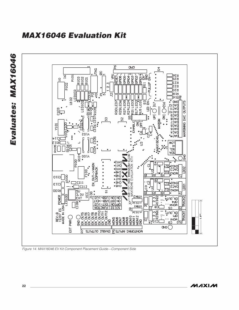
Figure 14. MAX16046 EV Kit Component Placement Guide—Component Side
Eva
lua
tes: M
AX
16
04
6
MAX16046 Evaluation Kit
______________________________________________________________________________________ 23
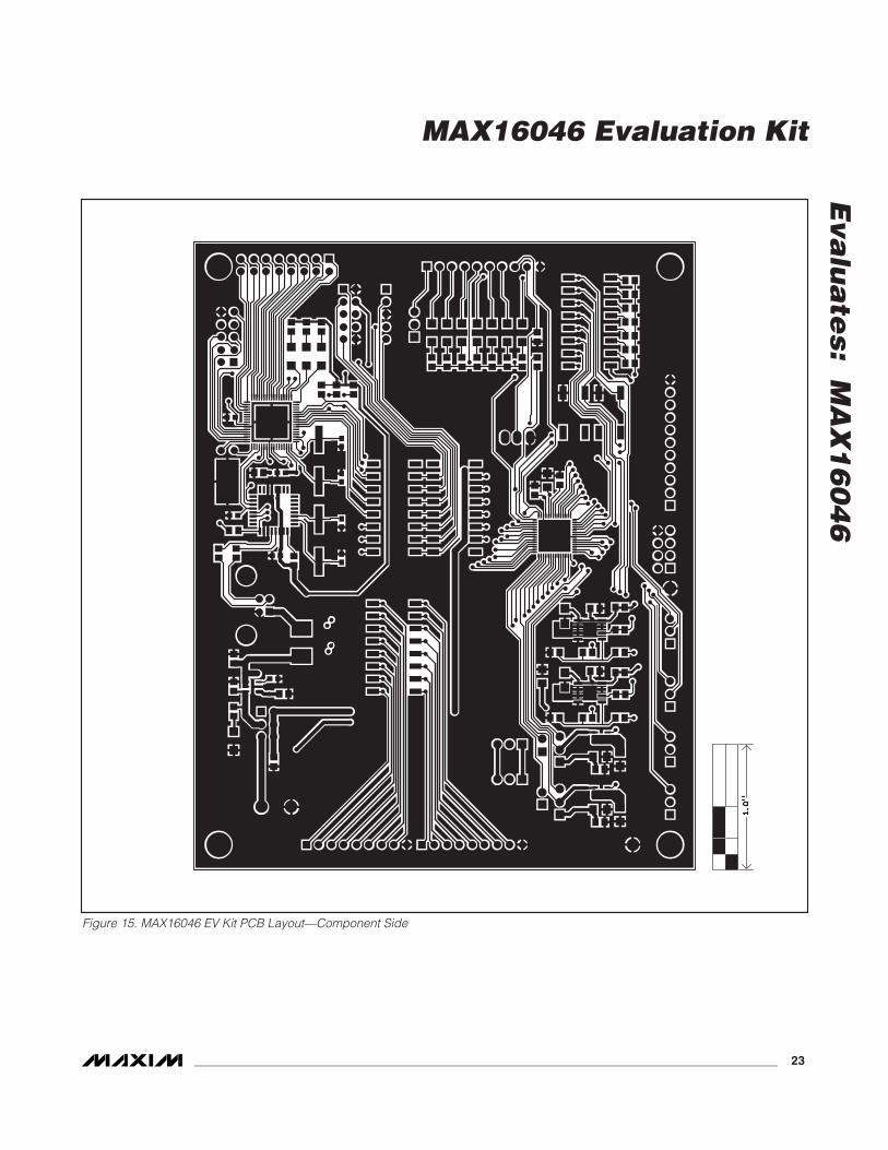
Figure 15. MAX16046 EV Kit PCB Layout—Component Side
Eva
lua
tes:
M
AX
16
04
6
MAX16046 Evaluation Kit
24 ______________________________________________________________________________________
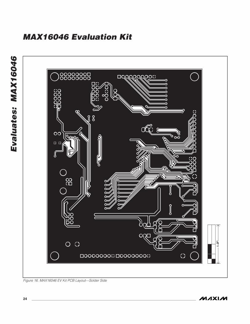
Figure 16. MAX16046 EV Kit PCB Layout—Solder Side

Maxim cannot assume responsibility for use of any circuitry other than circuitry entirely embodied in a Maxim product. No circuit patent licenses areimplied. Maxim reserves the right to change the circuitry and specifications without notice at any time.
Maxim Integrated Products, 120 San Gabriel Drive, Sunnyvale, CA 94086 408-737-7600 __________________ 25
© 2009 Maxim Integrated Products Maxim is a registered trademark of Maxim Integrated Products, Inc.
Eva
lua
tes: M
AX
16
04
6
MAX16046 Evaluation Kit
Revision History
REVISIONNUMBER
REVISIONDATE DESCRIPTION PAGES
CHANGED
0 2/08 Initial release —
1 3/09 Clarified I2C addresses in Table 5. 18


![[Manua]Tula Ev-kit Mr Sensor(Eng,060602)](https://img.pdfslide.us/doc/110x75/577d33fe1a28ab3a6b8c52d8/manuatula-ev-kit-mr-sensoreng060602.jpg)