Embed Size (px)
Citation preview
1
MAX3639 Evaluation Kit
Eva
lua
tes: M
AX
36
39
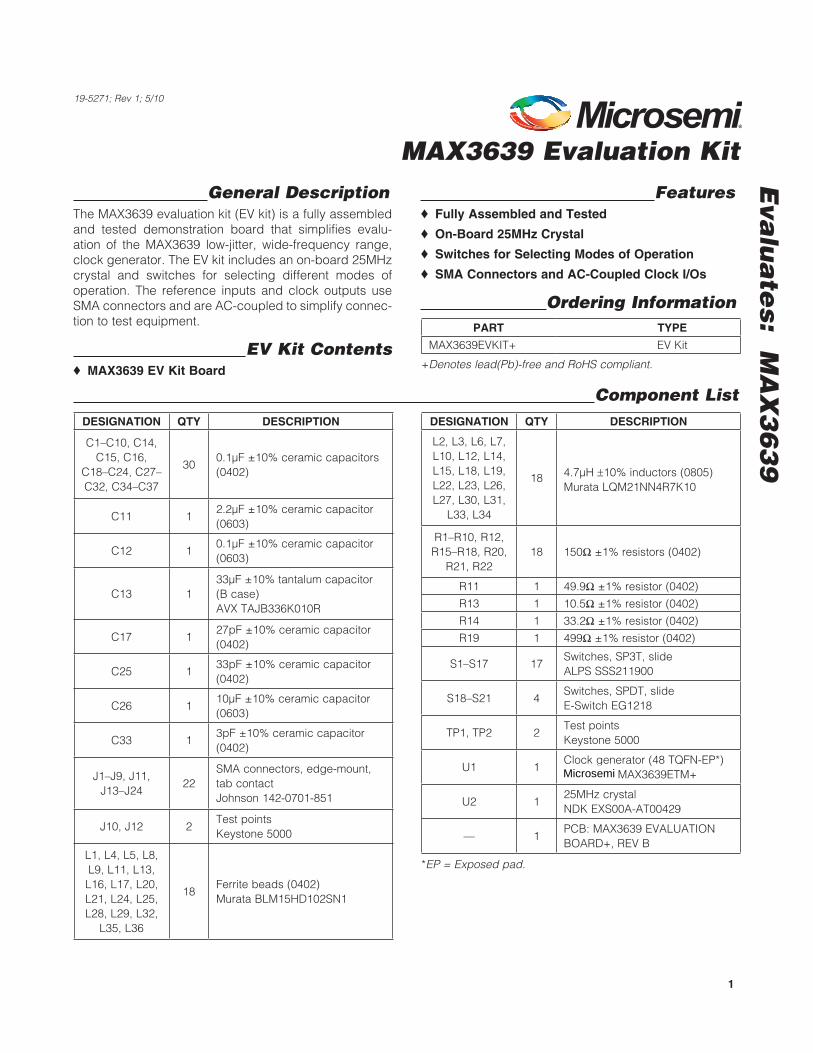
General DescriptionThe MAX3639 evaluation kit (EV kit) is a fully assembled and tested demonstration board that simplifies evalu-ation of the MAX3639 low-jitter, wide-frequency range, clock generator. The EV kit includes an on-board 25MHz crystal and switches for selecting different modes of operation. The reference inputs and clock outputs use SMA connectors and are AC-coupled to simplify connec-tion to test equipment.
EV Kit ContentsS MAX3639 EV Kit Board
FeaturesS Fully Assembled and Tested
S On-Board 25MHz Crystal
S Switches for Selecting Modes of Operation
S SMA Connectors and AC-Coupled Clock I/Os
Ordering Information
Component List
19-5271; Rev 1; 5/10
+Denotes lead(Pb)-free and RoHS compliant.
*EP = Exposed pad.
DESIGNATION QTY DESCRIPTION
C1–C10, C14, C15, C16,
C18–C24, C27–C32, C34–C37
300.1FF Q10% ceramic capacitors (0402)
C11 12.2FF Q10% ceramic capacitor (0603)
C12 10.1FF Q10% ceramic capacitor (0603)
C13 133FF Q10% tantalum capacitor (B case)AVX TAJB336K010R
C17 127pF Q10% ceramic capacitor (0402)
C25 133pF Q10% ceramic capacitor (0402)
C26 110FF Q10% ceramic capacitor (0603)
C33 13pF Q10% ceramic capacitor (0402)
J1–J9, J11, J13–J24
22SMA connectors, edge-mount, tab contactJohnson 142-0701-851
J10, J12 2Test pointsKeystone 5000
L1, L4, L5, L8, L9, L11, L13, L16, L17, L20, L21, L24, L25, L28, L29, L32,
L35, L36
18Ferrite beads (0402)Murata BLM15HD102SN1
DESIGNATION QTY DESCRIPTION
L2, L3, L6, L7, L10, L12, L14, L15, L18, L19, L22, L23, L26, L27, L30, L31,
L33, L34
18 4.7FH ±10% inductors (0805)Murata LQM21NN4R7K10
R1–R10, R12, R15–R18, R20,
R21, R2218 150I Q1% resistors (0402)
R11 1 49.9I Q1% resistor (0402)
R13 1 10.5I Q1% resistor (0402)
R14 1 33.2I Q1% resistor (0402)
R19 1 499I Q1% resistor (0402)
S1–S17 17Switches, SP3T, slideALPS SSS211900
S18–S21 4Switches, SPDT, slideE-Switch EG1218
TP1, TP2 2Test pointsKeystone 5000
U1 1Clock generator (48 TQFN-EP*)
Maxim MAX3639ETM+
U2 125MHz crystalNDK EXS00A-AT00429
— 1PCB: MAX3639 EVALUATION BOARD+, REV B
PART TYPE
MAX3639EVKIT+ EV Kit
E V A L U A T I O N K I T A V A I L A B L E
Microsemi
MAX3639 Evaluation Kit
Eva
lua
tes:
M
AX
36
39
2
Quick Start1) Set the switches to the following settings to generate
a 156.25MHz LVDS output from the 25MHz crystal reference:
IN_SEL = XO
PLL_BP = LOW
DM = LOW
DP1 = LOW, DP0 = HIGH
DF1 = LOW, DF0 = LOW
DA1 = HIGH, DA0 = LOW
DB1 = HIGH, DB0 = LOW
DC1 = HIGH, DC0 = LOW
QA_CTRL1 = LVDS
QA_CTRL2 = DISABLED
QB_CTRL = DISABLED
QC_CTRL = DISABLED
QA_TERM1 = LVDS
QA_TERM2 = LVDS
QB_TERM = LVDS
QC_TERM = LVDS
2) Connect a +3.3V supply to VCC (J10) and GND (J12). Set the supply current limit to 500mA.
3) Using SMA cables, connect QA0 (J11) and QA0 (J13) to a phase noise analyzer or scope. Terminate all unused enabled outputs, QA1 (J14), QA1 (J15), QA2 (J16), and QA2 (J17).
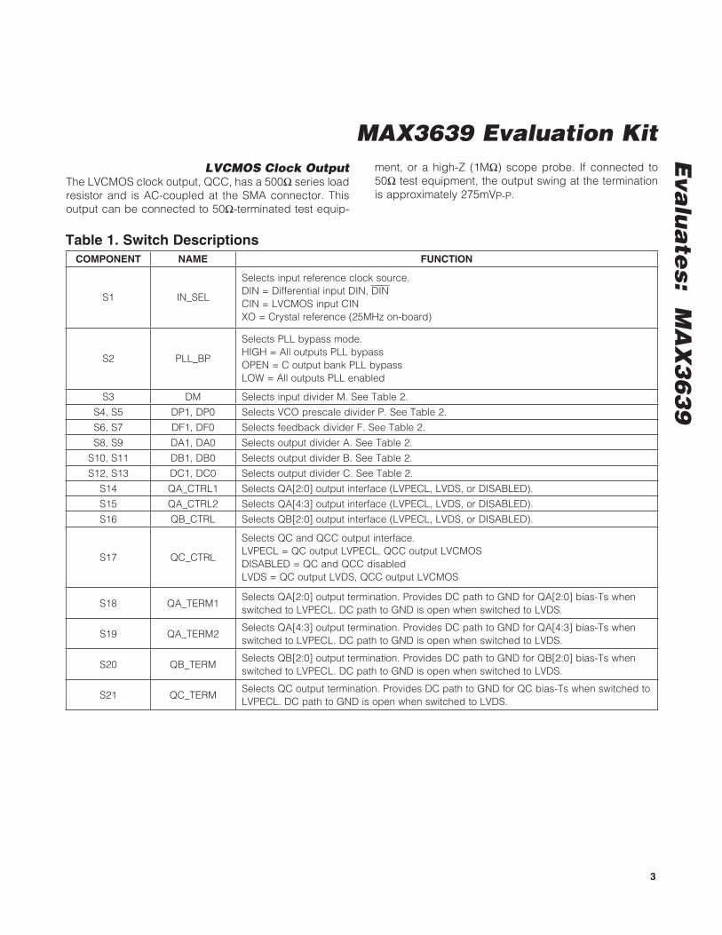
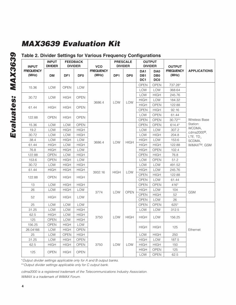
Detailed DescriptionThe MAX3639 EV kit simplifies evaluation by providing the hardware needed to evaluate all the MAX3639 func-tions. Table 1 contains functional descriptions for the switches. Table 2 provides the divider settings for vari-ous frequency configurations.
LVCMOS Clock InputThe LVCMOS clock input, CIN, is AC-coupled at the SMA connector and has an on-board 50I termination. For optimal performance it is important to use a low-jitter square-wave clock source. Clock signals should be applied to CIN only when the switch IN_SEL is set to CIN.
Differential Clock InputThe differential clock input, DIN, is AC-coupled at the SMA connectors and has an internal 100I differential termination. For optimal performance it is important to use a low-jitter, differential, square-wave clock source. Clock signals should be applied to DIN only when the switch IN_SEL is set to DIN.
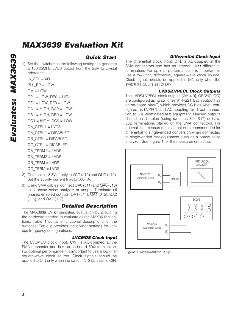
LVDS/LVPECL Clock OutputsThe LVDS/LVPECL clock outputs (QA[4:0], QB[2:0], QC) are configured using switches S14–S21. Each output has an on-board bias-T, which provides DC bias when con-figured as LVPECL and AC-coupling for direct connec-tion to 50I-terminated test equipment. Unused outputs should be disabled (using switches S14–S17) or have 50I terminations placed on the SMA connectors. For optimal jitter measurements, a balun is recommended for differential to single-ended conversion when connected to single-ended test equipment such as a phase noise analyzer. See Figure 1 for the measurement setup.
Figure 1. Measurement Setup
EVALUATION BOARD BALUN
PHASE NOISEANALYZER
Q_
Q_
SCOPE
MAX3639
EVALUATION BOARDQ_
Q_
MAX3639
MAX3639 Evaluation Kit
Eva
lua
tes: M
AX
36
39
3
Table 1. Switch Descriptions
LVCMOS Clock OutputThe LVCMOS clock output, QCC, has a 500I series load resistor and is AC-coupled at the SMA connector. This output can be connected to 50I-terminated test equip-
ment, or a high-Z (1MI) scope probe. If connected to 50I test equipment, the output swing at the termination is approximately 275mVP-P.
COMPONENT NAME FUNCTION
S1 IN_SEL
Selects input reference clock source.DIN = Differential input DIN, DINCIN = LVCMOS input CINXO = Crystal reference (25MHz on-board)
S2 PLL_BP
Selects PLL bypass mode.HIGH = All outputs PLL bypassOPEN = C output bank PLL bypassLOW = All outputs PLL enabled
S3 DM Selects input divider M. See Table 2.
S4, S5 DP1, DP0 Selects VCO prescale divider P. See Table 2.
S6, S7 DF1, DF0 Selects feedback divider F. See Table 2.
S8, S9 DA1, DA0 Selects output divider A. See Table 2.
S10, S11 DB1, DB0 Selects output divider B. See Table 2.
S12, S13 DC1, DC0 Selects output divider C. See Table 2.
S14 QA_CTRL1 Selects QA[2:0] output interface (LVPECL, LVDS, or DISABLED).
S15 QA_CTRL2 Selects QA[4:3] output interface (LVPECL, LVDS, or DISABLED).
S16 QB_CTRL Selects QB[2:0] output interface (LVPECL, LVDS, or DISABLED).
S17 QC_CTRL
Selects QC and QCC output interface.LVPECL = QC output LVPECL, QCC output LVCMOSDISABLED = QC and QCC disabledLVDS = QC output LVDS, QCC output LVCMOS
S18 QA_TERM1Selects QA[2:0] output termination. Provides DC path to GND for QA[2:0] bias-Ts when switched to LVPECL. DC path to GND is open when switched to LVDS.
S19 QA_TERM2Selects QA[4:3] output termination. Provides DC path to GND for QA[4:3] bias-Ts when switched to LVPECL. DC path to GND is open when switched to LVDS.
S20 QB_TERMSelects QB[2:0] output termination. Provides DC path to GND for QB[2:0] bias-Ts when switched to LVPECL. DC path to GND is open when switched to LVDS.
S21 QC_TERMSelects QC output termination. Provides DC path to GND for QC bias-Ts when switched to LVPECL. DC path to GND is open when switched to LVDS.
MAX3639 Evaluation Kit
Eva
lua
tes:
M
AX
36
39
4
Table 2. Divider Settings for Various Frequency Configurations
*Output divider settings applicable only for A and B output banks.**Output divider settings applicable only for C output bank.
cdma2000 is a registered trademark of the Telecommunications Industry Association.
WiMAX is a trademark of WiMAX Forum.
INPUT FREQUENCY
(MHz)
INPUT DIVIDER
FEEDBACK DIVIDER VCO
FREQUENCY(MHz)
PRESCALE DIVIDER
OUTPUT DIVIDER OUTPUT
FREQUENCY(MHz)
APPLICATIONSDM DF1 DF0 DP1 DP0
DA1 DB1 DC1
DA0 DB0 DC0
15.36 LOW OPEN LOW
3686.4 LOW LOW
OPEN OPEN 737.28*
Wireless Base Station:WCDMA, cdma2000®, LTE, TD_SCDMA, WiMAXTM, GSM
LOW LOW 368.64
30.72 LOW HIGH OPENLOW HIGH 245.76
HIGH LOW 184.32
61.44 HIGH HIGH OPENHIGH OPEN 122.88
OPEN HIGH 92.16
122.88 OPEN HIGH OPENLOW OPEN 61.44
OPEN OPEN 30.72**
15.36 LOW LOW OPEN
3686.4 LOW HIGH
OPEN OPEN 614.4*
19.2 LOW HIGH HIGH LOW LOW 307.2
30.72 LOW LOW HIGH LOW HIGH 204.8
38.4 LOW HIGH LOW HIGH LOW 153.6
61.44 HIGH LOW HIGH HIGH HIGH 122.88
76.8 HIGH HIGH LOW HIGH OPEN 102.4
122.88 OPEN LOW HIGH OPEN HIGH 76.8
153.6 OPEN HIGH LOW LOW OPEN 51.2
30.72 LOW HIGH HIGH
3932.16 HIGH LOW
LOW LOW 491.52
61.44 HIGH HIGH HIGH HIGH LOW 245.76
122.88 OPEN HIGH HIGHOPEN HIGH 122.88
OPEN LOW 61.44
13 LOW HIGH HIGH
3774 LOW OPEN
OPEN OPEN 416*
GSM26 LOW HIGH LOW HIGH LOW 104
52 HIGH HIGH LOWOPEN HIGH 52
OPEN LOW 26
25 LOW LOW LOW
3750 LOW HIGH
OPEN OPEN 625*
Ethernet
31.25 LOW LOW HIGH LOW LOW 312.5
62.5 HIGH LOW HIGHHIGH LOW 156.25
125 OPEN LOW HIGH
156.25 OPEN HIGH LOWHIGH HIGH 125
26.04166 LOW HIGH OPEN
25 LOW OPEN HIGH
3750 LOW LOW
LOW HIGH 250
31.25 LOW HIGH OPEN HIGH LOW 187.5
62.5 HIGH HIGH OPEN HIGH HIGH 150
125 OPEN HIGH OPENHIGH OPEN 125
LOW OPEN 62.5
MAX3639 Evaluation Kit
Eva
lua
tes: M
AX
36
39
5
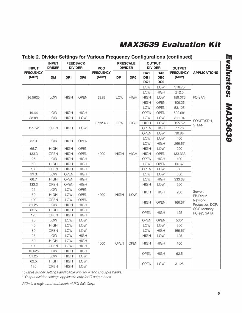
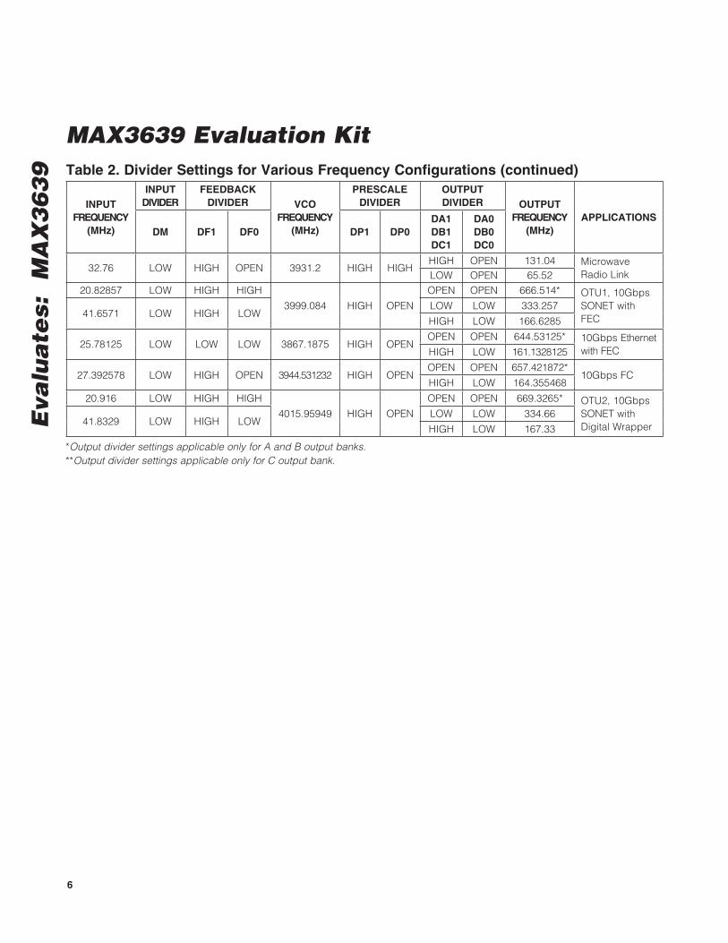
Table 2. Divider Settings for Various Frequency Configurations (continued)
*Output divider settings applicable only for A and B output banks.**Output divider settings applicable only for C output bank.
PCIe is a registered trademark of PCI-SIG Corp.
INPUT FREQUENCY
(MHz)
INPUT DIVIDER
FEEDBACK DIVIDER VCO
FREQUENCY(MHz)
PRESCALE DIVIDER
OUTPUT DIVIDER OUTPUT
FREQUENCY(MHz)
APPLICATIONSDM DF1 DF0 DP1 DP0
DA1 DB1 DC1
DA0 DB0 DC0
26.5625 LOW HIGH OPEN 3825 LOW HIGH
LOW LOW 318.75
FC-SAN
LOW HIGH 212.5
HIGH LOW 159.375
HIGH OPEN 106.25
LOW OPEN 53.125
19.44 LOW HIGH HIGH
3732.48 LOW HIGH
OPEN OPEN 622.08*
SONET/SDH, STM-N
38.88 LOW HIGH LOW LOW LOW 311.04
155.52 OPEN HIGH LOW
HIGH LOW 155.52
OPEN HIGH 77.76
OPEN LOW 38.88
33.3 LOW HIGH OPEN
4000 HIGH HIGH
LOW LOW 400
Server, FB-DIMM, Network Processor, DDR/QDR Memory, PCIe®, SATA
LOW HIGH 266.67
66.7 HIGH HIGH OPEN HIGH LOW 200
133.3 OPEN HIGH OPEN HIGH OPEN 133.333
25 LOW HIGH HIGH OPEN HIGH 100
50 HIGH HIGH HIGH LOW OPEN 66.67
100 OPEN HIGH HIGH OPEN LOW 50
33.3 LOW OPEN HIGH
4000 HIGH LOW
LOW LOW 500
66.7 HIGH OPEN HIGH LOW HIGH 333.33
133.3 OPEN OPEN HIGH HIGH LOW 250
25 LOW LOW OPENHIGH HIGH 200
50 HIGH LOW OPEN
100 OPEN LOW OPENHIGH OPEN 166.67
31.25 LOW HIGH HIGH
62.5 HIGH HIGH HIGHOPEN HIGH 125
125 OPEN HIGH HIGH
20 LOW LOW LOW
4000 OPEN OPEN
OPEN OPEN 500*
40 HIGH LOW LOW LOW LOW 250
80 OPEN LOW LOW LOW HIGH 166.67
25 LOW LOW HIGH HIGH LOW 125
50 HIGH LOW HIGHHIGH HIGH 100
100 OPEN LOW HIGH
15.625 LOW HIGH HIGHOPEN HIGH 62.5
31.25 LOW HIGH LOW
62.5 HIGH HIGH LOWOPEN LOW 31.25
125 OPEN HIGH LOW
MAX3639 Evaluation Kit
Eva
lua
tes:
M
AX
36
39
6
Table 2. Divider Settings for Various Frequency Configurations (continued)
*Output divider settings applicable only for A and B output banks.**Output divider settings applicable only for C output bank.
INPUT FREQUENCY
(MHz)
INPUT DIVIDER
FEEDBACK DIVIDER VCO
FREQUENCY(MHz)
PRESCALE DIVIDER
OUTPUT DIVIDER OUTPUT
FREQUENCY(MHz)
APPLICATIONSDM DF1 DF0 DP1 DP0
DA1 DB1 DC1
DA0 DB0 DC0
32.76 LOW HIGH OPEN 3931.2 HIGH HIGHHIGH OPEN 131.04 Microwave
Radio LinkLOW OPEN 65.5220.82857 LOW HIGH HIGH
3999.084 HIGH OPEN
OPEN OPEN 666.514* OTU1, 10Gbps SONET with FEC41.6571 LOW HIGH LOW
LOW LOW 333.257
HIGH LOW 166.6285
25.78125 LOW LOW LOW 3867.1875 HIGH OPENOPEN OPEN 644.53125* 10Gbps Ethernet
with FECHIGH LOW 161.1328125
27.392578 LOW HIGH OPEN 3944.531232 HIGH OPENOPEN OPEN 657.421872*
10Gbps FCHIGH LOW 164.355468
20.916 LOW HIGH HIGH
4015.95949 HIGH OPEN
OPEN OPEN 669.3265* OTU2, 10Gbps SONET with Digital Wrapper41.8329 LOW HIGH LOW
LOW LOW 334.66
HIGH LOW 167.33
MAX3639 Evaluation Kit
Eva
lua
tes: M
AX
36
39
7
Figure 2. MAX3639 EV Kit Schematic
DMXINXOUTVCCIN_SELPLL_BPDF1DF0QC_CTRLVCCADP1DP0
VCCQAQA0QA0QA1QA1QA2QA2QA3QA3QA4QA4
VCCQA
DB1
DB0
DA1
DA0
DC1
DC0
QA_C
TRL2
VCCQ
CCQC
CQC QC VC
CQC
CIN
DIN
DIN
QB_C
TRL
QA_C
TRL1
QB2
QB2
QB1
QB1
QB0
QB0
VCCQ
B
123456789
101112
U1
MAX3639ETM+
EP
363534333231302928272625
48 47 46 45 44 43 42 41 40 39 38 37
13 14 15 16 17 18 19 20 21 22 23 24
DM
25MHzCRYSTAL
U2
C2533pF
IN_SELPLL_BP
DF1DF0
QC_CTRL
DP1DP0
C230.1uF
C2610uF
R1310.5Ω
1%
C240.1uF
VCC
C1727pF
VCC
GNDJ10
J12
C112.2uF
C120.1uF
VCCTP1
TP2C1333uF
C180.1uF
VCC R1149.9Ω
1%C19
0.1uF
C10.1uF
C20.1uF
C30.1uF
CINJ1
DINJ2
DINJ3
+3.3V
DB1
DB0
DA1
DA0
DC1
DC0
QA_C
TRL2
QA_C
TRL1
QB_C
TRL
C210.1uF
VCC
C200.1uF
VCC
C40.1uF
C50.1uF
QB2J4
QB2J5
QB_TERM
C60.1uF
C70.1uF
QB1J6
QB1J7
QB_TERM
C80.1uF
C90.1uF
QB0J8
QB0J9
QB_TERM
C100.1uF
C140.1uF
QA0J11
QA0J13
QA_TERM1
C150.1uF
C160.1uF
QA1J14
QA1J15
QA_TERM1
C220.1uF
C290.1uF
QA2J16
QA2J17
QA_TERM1
C300.1uF
C310.1uF
QA3J18
QA3J19
QA_TERM2
C320.1uF
C370.1uF
QA4J20
QA4J24
QA_TERM2
VCC
C270.1uF
C280.1uF
R1433.2Ω
1%
C333pF
R19499Ω
1%
C340.1uF
QCCJ21
C350.1uF
C360.1uF
QCJ22
QCJ23
R20150Ω 1%
L32FERRITE BEAD
L334.7uH
R21150Ω 1%
L35FERRITE BEAD
L344.7uH
QC_TERM
VCC
IN_SEL S1
DM
VCC
PLL_BPS2
VCC
S3
DP0
VCC
DP1S4
VCC
S5DF0
VCC
DF1S6
VCC
S7
DA0
VCC
DA1S8
VCC
S9DB0
VCC
DB1S10
VCC
S11DC0
VCC
DC1S12
VCC
S13
VCC
QA_CTRL1S14
VCC
S15QC_CTRL
VCC
QB_CTRLS16
VCC
S17QA_CTRL2
QA_TERM1S18
QA_TERM2S19
QB_TERMS20
QC_TERMS21
R1150Ω 1%
L1FERRITE BEAD
L24.7uH
R2150Ω 1%
L4FERRITE BEAD
L34.7uH
R3150Ω 1%
L5FERRITE BEAD
L64.7uH
R4150Ω 1%
L8FERRITE BEAD
L74.7uH
R5150Ω 1%
L9FERRITE BEAD
L104.7uH
R6150Ω 1%
L11FERRITE BEAD
L124.7uH
R7150Ω 1%
L13FERRITE BEAD
L144.7uH
R8150Ω 1%
L16FERRITE BEAD
L154.7uH
R9150Ω 1%
L17FERRITE BEAD
L184.7uH
R10150Ω 1%
L20FERRITE BEAD
L194.7uH
R12150Ω 1%
L21FERRITE BEAD
L224.7uH
R15150Ω 1%
L24FERRITE BEAD
L234.7uH
R16150Ω 1%
L25FERRITE BEAD
L264.7uH
R17150Ω 1%
L28FERRITE BEAD
L274.7uH
R18150Ω 1%
L29FERRITE BEAD
L304.7uH
R22150Ω 1%
L314.7uH
L36FERRITE BEAD
MAX3639 Evaluation Kit
Eva
lua
tes:
M
AX
36
39
8
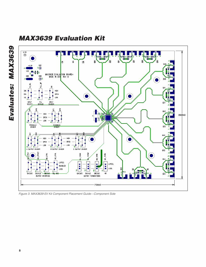
Figure 3. MAX3639 EV Kit Component Placement Guide—Component Side
MAX3639 Evaluation Kit
Eva
lua
tes: M
AX
36
39
9
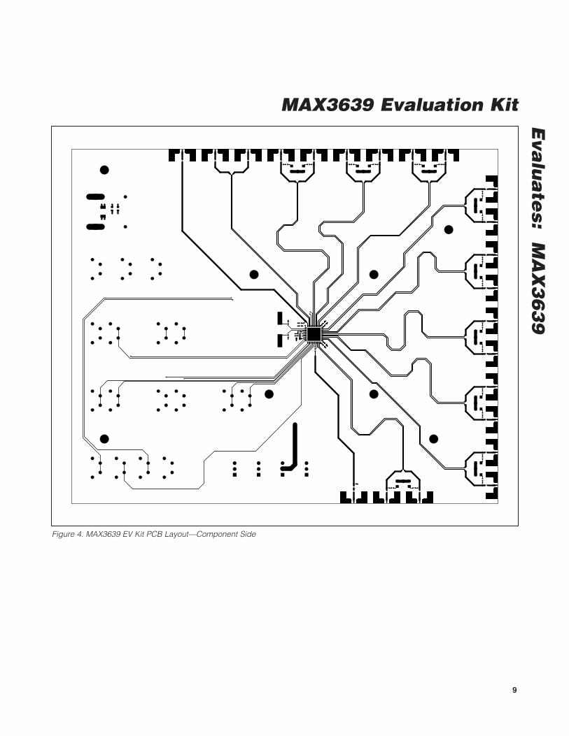
Figure 4. MAX3639 EV Kit PCB Layout—Component Side
MAX3639 Evaluation Kit
Eva
lua
tes:
M
AX
36
39
10
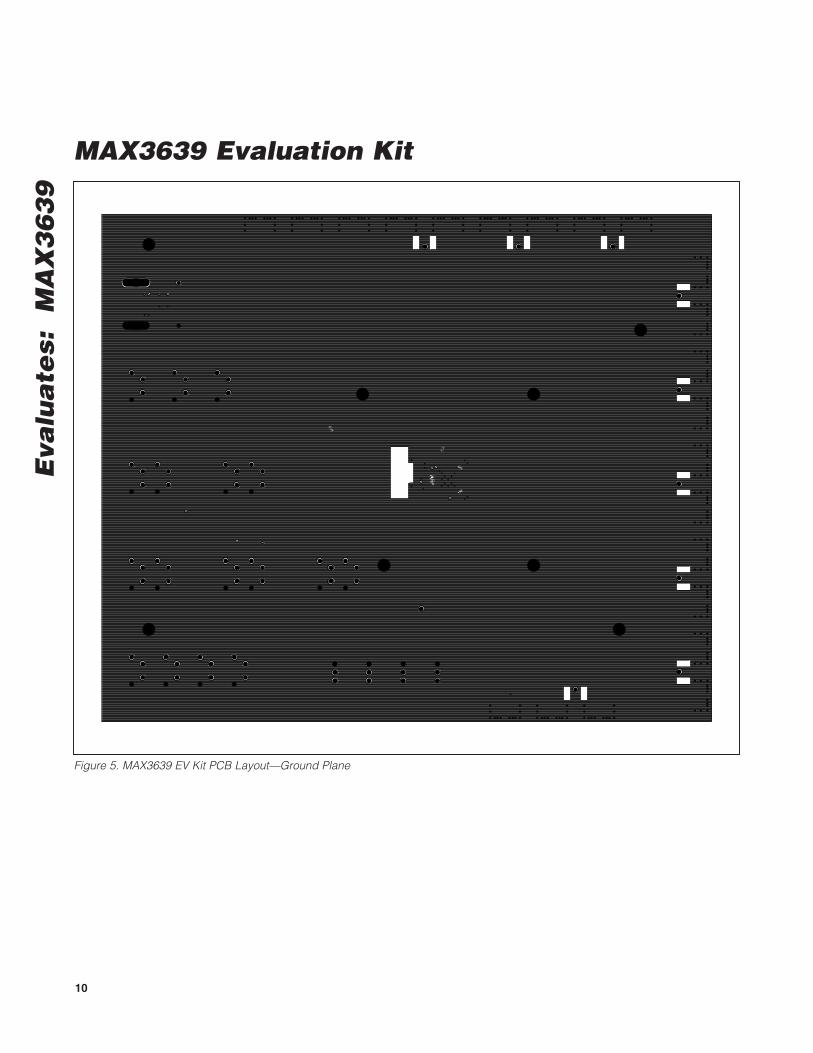
Figure 5. MAX3639 EV Kit PCB Layout—Ground Plane
MAX3639 Evaluation Kit
Eva
lua
tes: M
AX
36
39
11
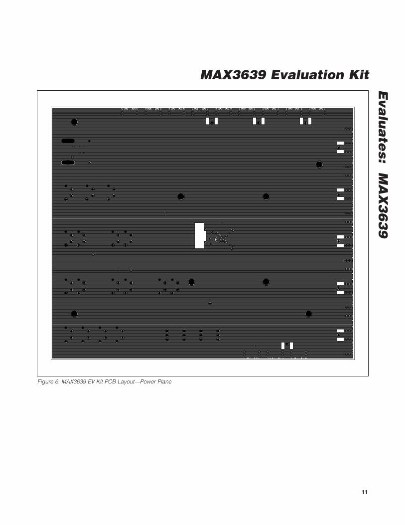
Figure 6. MAX3639 EV Kit PCB Layout—Power Plane
MAX3639 Evaluation Kit
Eva
lua
tes:
M
AX
36
39
12
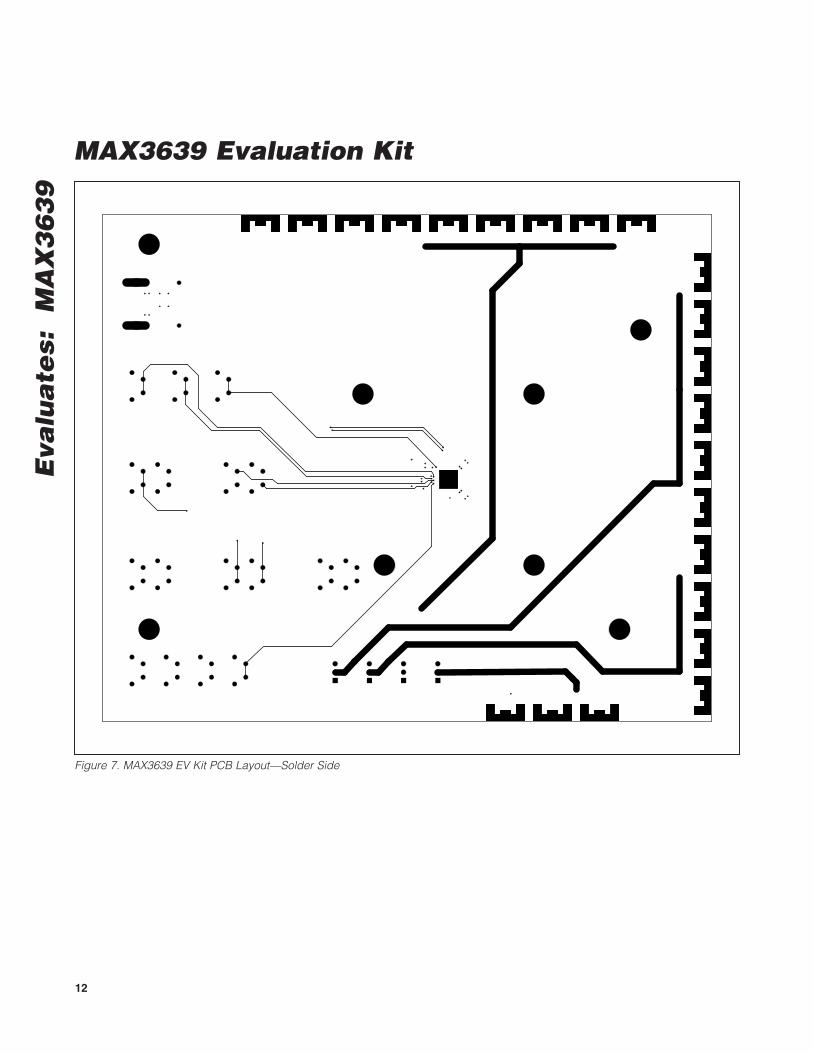
Figure 7. MAX3639 EV Kit PCB Layout—Solder Side
13
MAX3639 Evaluation Kit
Eva
lua
tes: M
AX
36
39
Revision HistoryREVISIONNUMBER
REVISIONDATE
DESCRIPTIONPAGES
CHANGED
0 5/10 Initial release —
1 5/10Changed R13 from 10.0Ω to 10.5Ω in the Component List and Figure 2; corrected the label for L28 in Figure 2
1, 7

Microsemi Corporate Headquarters One Enterprise, Aliso Viejo CA 92656 USA Within the USA: +1 (949) 380-6100 Sales: +1 (949) 380-6136 Fax: +1 (949) 215-4996
Microsemi Corporation (NASDAQ: MSCC) offers a comprehensive portfolio of semiconductor solutions for: aerospace, defense and security; enterprise and communications; and industrial and alternative energy markets. Products include high-performance, high-reliability analog and RF devices, mixed signal and RF integrated circuits, customizable SoCs, FPGAs, and complete subsystems. Microsemi is headquartered in Aliso Viejo, Calif. Learn more at www.microsemi.com.
© 2012 Microsemi Corporation. All rights reserved. Microsemi and the Microsemi logo are trademarks of Microsemi Corporation. All other trademarks and service marks are the property of their respective owners.