Embed Size (px)
Citation preview

_______________________________________________________________ Maxim Integrated Products 1
For pricing, delivery, and ordering information, please contact Maxim Direct at 1-888-629-4642, or visit Maxim’s website at www.maxim-ic.com.
MAX9530 Evaluation Kit
Eva
lua
tes: M
AX
95
30
General DescriptionThe MAX9530 evaluation kit (EV kit) provides a proven design to evaluate the MAX9530 quad NTSC/PAL decoder and quad audio codec. The EV kit also includes Windows XPM-, Windows VistaM-, and WindowsM 7-com-patible software that provides a graphical user interface (GUI) for exercising the features of the IC.
The EV kit comes with a MAX9530CXV+ installed.
FeaturesS Accepts Single-Ended or Differential Video
S Accepts Single-Ended or Differential Audio
S On-Board Frame Buffer Memory
S Digital Output Routing Through FPGA
S Digital Outputs Directly Drive FMC Connector
S Analog Audio Output Buffers
S Analog Video DAC
S Serial Digital Video Output Buffer at 270Mbps
S Windows XP-, Windows Vista-, and Windows 7-Compatible Software
S USB-PC Connection (Cable Included)
S Proven PCB Layout
S Fully Assembled and Tested
S Requires Single 5V Power Supply
Ordering Information
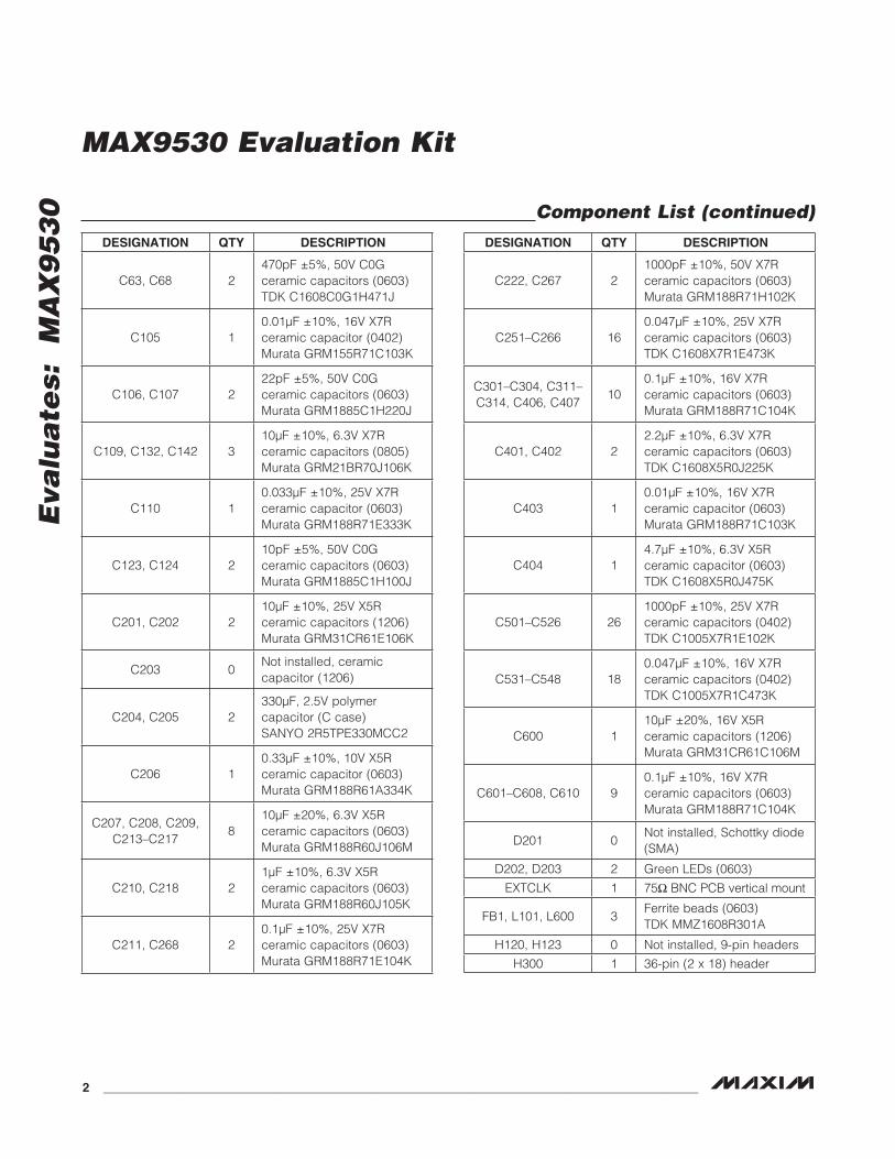
Component List
19-5656; Rev 0; 12/10
+Denotes lead(Pb)-free and RoHS compliant.
Windows, Windows XP, and Windows Vista are registered trademarks of Microsoft Corp.
PART TYPE
MAX9530EVKIT+ EV Kit
DESIGNATION QTY DESCRIPTION
5V_IN, PGND 2 Banana jacks
AIN1–AIN4, AOUT1, AOUT2
6 Right-angle RCA jacks, white
AIN1N–AIN4N, AIN1P–AIN4P, GNDA, GNDV, VIN1N–VIN4N, VIN1P–VIN4P
1820G tinned copper bus wire into U-shape loops (0.25in off the PCB)
C1–C11, C212, C219, C220, C221,
C2230
Not installed, ceramic capacitors (0603)
C12, C13 227pF Q5%, 50V C0G ceramic capacitors (0603)TDK C1608C0G1H270J
C14–C21, C66, C100–C104, C111,
C121, C12217
0.1FF Q10%, 25V X7R ceramic capacitors (0603)TDK C1608X7R1E104K
DESIGNATION QTY DESCRIPTION
C22–C45, C47, C50, C73
270.1FF Q10%, 6.3V X5R ceramic capacitors (0201)TDK C0603X5R0J104K
C46, C49, C71 30.01FF Q10%, 6.3V X5R ceramic capacitors (0201)Murata GRM033R60J103K
C48, C51, C60, C61, C74, C108,
C131, C141, C550, C551, C560, C561
121FF Q10%, 16V X7R ceramiccapacitors (0603) TDK C1608X7R1C105K
C52–C59 80.47FF Q10%, 25V X7R ceramic capacitors (0603) Murata GRM188R71E474K
C62, C64, C65, C67, C69, C70,
C727
2.2FF Q10%, 10V X7R ceramic capacitors (0603) Murata GRM188R71A225K
MAX9530 Evaluation Kit
Eva
lua
tes:
M
AX
95
30
2 ______________________________________________________________________________________
Component List (continued)
DESIGNATION QTY DESCRIPTION
C63, C68 2470pF Q5%, 50V C0G ceramic capacitors (0603)TDK C1608C0G1H471J
C105 10.01FF Q10%, 16V X7R ceramic capacitor (0402)Murata GRM155R71C103K
C106, C107 222pF Q5%, 50V C0Gceramic capacitors (0603)Murata GRM1885C1H220J
C109, C132, C142 310FF Q10%, 6.3V X7R ceramic capacitors (0805)Murata GRM21BR70J106K
C110 10.033FF Q10%, 25V X7R ceramic capacitor (0603)Murata GRM188R71E333K
C123, C124 210pF Q5%, 50V C0Gceramic capacitors (0603)Murata GRM1885C1H100J
C201, C202 210FF Q10%, 25V X5Rceramic capacitors (1206)Murata GRM31CR61E106K
C203 0Not installed, ceramic capacitor (1206)
C204, C205 2330FF, 2.5V polymercapacitor (C case)SANYO 2R5TPE330MCC2
C206 10.33FF Q10%, 10V X5R ceramic capacitor (0603)Murata GRM188R61A334K
C207, C208, C209, C213–C217
810FF Q20%, 6.3V X5R ceramic capacitors (0603)Murata GRM188R60J106M
C210, C218 21FF Q10%, 6.3V X5Rceramic capacitors (0603)Murata GRM188R60J105K
C211, C268 20.1FF Q10%, 25V X7R ceramic capacitors (0603)Murata GRM188R71E104K
DESIGNATION QTY DESCRIPTION
C222, C267 21000pF Q10%, 50V X7R ceramic capacitors (0603)Murata GRM188R71H102K
C251–C266 160.047FF Q10%, 25V X7Rceramic capacitors (0603)TDK C1608X7R1E473K
C301–C304, C311–C314, C406, C407
100.1FF Q10%, 16V X7Rceramic capacitors (0603)Murata GRM188R71C104K
C401, C402 22.2FF Q10%, 6.3V X7R ceramic capacitors (0603)TDK C1608X5R0J225K
C403 10.01FF Q10%, 16V X7R ceramic capacitor (0603)Murata GRM188R71C103K
C404 14.7FF Q10%, 6.3V X5R ceramic capacitor (0603)TDK C1608X5R0J475K
C501–C526 261000pF Q10%, 25V X7R ceramic capacitors (0402)TDK C1005X7R1E102K
C531–C548 180.047FF Q10%, 16V X7Rceramic capacitors (0402)TDK C1005X7R1C473K
C600 110FF Q20%, 16V X5Rceramic capacitors (1206)Murata GRM31CR61C106M
C601–C608, C610 90.1FF Q10%, 16V X7R ceramic capacitors (0603)Murata GRM188R71C104K
D201 0Not installed, Schottky diode (SMA)
D202, D203 2 Green LEDs (0603)
EXTCLK 1 75I BNC PCB vertical mount
FB1, L101, L600 3Ferrite beads (0603)TDK MMZ1608R301A
H120, H123 0 Not installed, 9-pin headers
H300 1 36-pin (2 x 18) header

MAX9530 Evaluation Kit
Eva
lua
tes: M
AX
95
30
_______________________________________________________________________________________ 3
Component List (continued)
DESIGNATION QTY DESCRIPTION
H350 1FMC connector, low-density, 0.050in pitch socket array Samtec ASP-134603-01
H501, H503 2 16-pin (2 x 8) headers
H502 1 26-pin (2 x 13) header
H600 1 2-pin header
JTAGU1, JTAGU120
0Not installed, 10-pin (2 x 5) headers
JTAGU500 1 6-pin header
JU1–JU24, JU26–JU30, JU201,
JU203–JU209, JU350, JU500, JU501, JU502, JU506, JU507, JU550, JU551, JU560, JU561, JU601, JU602,
JU603
50 2-pin headers
JU101–JU108 0Not installed, 2-pin headers—shorted with PCB trace
JU202, JU600 2 3-pin headers
JU25, JU31 2 5-pin headers
L200 11.4FH Q30%, 12A, 3.4M
inductorSumida CDEP105NP-1R4
LED503, LED504 2 Red LEDs (0805)
LEDPWR 1 Red LED (0805)
N201 1n-channel MOSFET (8 SO)Fairchild FDMS7692
N202 1n-channel MOSFET (8 SO)Fairchild FDMS8660S
N203 0Not installed, dual MOSFET (8 SO)
NSOUT, SOUT 2 SMA connectors
PGOOD1, PGOOD2 0Not installed, multipurpose test points
Q100 1p-channel MOSFET (SOT223) Fairchild NDT456P
R1–R11 11 0I Q5% resistors (0603)
DESIGNATION QTY DESCRIPTION
R12–R16, R18, R209–R212, R214–
R2200
Not installed, resistors (0603)R209–R212 are shorted with PCB trace; all others are open
R17, R36–R51, R54, R55, R56, R60, R61, R62, R64–R67, R71
28 4.7kI Q5% resistors (0603)
R19 1 49.9kI Q1% resistor (0603)
R20–R35, R608–R613, R561
23 37.4I Q1% resistors (0603)
R52, R53, R57, R58, R59, R63,
R2137 10I Q5% resistors (0603)
R68, R72, R112, R500, R501, R502
6 10kI Q5% resistors (0603)
R69, R70 2 22I Q5% resistors (0402)
R100, R202, R203 3 1kI Q5% resistors (0603)
R101, R102 2 27I Q5% resistors (0603)
R103 1 1.5kI Q5% resistor (0603)
R104, R504 2 470I Q5% resistors (0603)
R111 1 2.2kI Q5% resistor (0603)
R201 10.002I Q1% resistor (2010)Vishay WSL20102L000FEA
R204–R207, R600, R601
6 100kI Q5% resistors (0603)
R208 1 200kI Q1% resistor (0603)
R401, R402 2 75I Q1% resistors (0603)
R403, R404 2 110I Q1% resistors (0603)
R405, R406 2 232I Q1% resistors (0603)
R503 1 680I Q5% resistor (0603)
R505, R506, R507 3 4.7kI Q5% resistors (0603)
R562 1 75kI Q1% resistor (0603)
R602 1 150I Q5% resistor (0603)
R603, R605, RTCK, RTDI, RTDO, RTMS
6 100I Q5% resistors (0603)
R604 1 4.02kI Q1% resistor (0603)
R606, R607, R615, R616, R617
5 75I Q5% resistors (0603)
RLEDPWR 1 330I Q5% resistor (0603)

MAX9530 Evaluation Kit
Eva
lua
tes:
M
AX
95
30
4 ______________________________________________________________________________________
Component List (continued)
µMAX is a registered trademark of Maxim Integrated Products, Inc.
DESIGNATION QTY DESCRIPTION
RN1–RN6 6
22I Q2% x 8 independent resistors array (0402 x 8 convex) Panasonic EXB-2HV220JV
SW_RESET 1 Momentary NO switch
TP3–TP8 6White multipurpose test points
TP00, TP100, TP101, TP108, TP132, TP142
0Not installed, multipurpose test points
TP201, TP202 2 Red multipurpose test points
TP403, TP404, TP405
0Not installed, multipurpose test points
U/BLUE, V/RED, Y/GREEN
3 Right-angle RCA jacks
U1 1Video and audio encoder (CSBGA 196) Maxim MAX9530CXV+
U2 1
Dual op amp, 5V single-supply unity-gain-stable (8 SOT23)Maxim LMX358AKA+(Top Mark: AAIR)
U100 1UART-to-USB converter (32 TQFP)
U110 193C46 type 3-wire EEPROM 16-bit architecture (8 SO)
U120 1Low-power microcontroller (68 QFN-EP) Maxim MAXQ2000-RAX+
U130 12.5V regulator (5 SC70)Maxim MAX8511EXK25+T(Top Mark: ADV)
U140 13.3V regulator (5 SC70)Maxim MAX8511EXK33+T(Top Mark: AEI)
DESIGNATION QTY DESCRIPTION
U200 1
Maxim complete power solution for DDR, DDR2, and DDR3 memory (24 TQFN)Maxim MAX17000ETG+
U250 1
360MHz DDR2 memory, 4M x 16 x 4 (84 FBGA)Micron MT47H16M16BG-37E:B
U300, U310 2Low-voltage TTL buffers (48 TSSOP)
U400 1SMPTE 259M 270MHz cable driver National Semi CLC006
U500 1
FPGA, Spartan-3AN, 200k, nonvolatile configuration (256 FBGA)Xilinx XC3S200AN-5FTG256C
U500TCK, U500TDI, U500TDO, U500TMS
4White multipurpose test points
U550, U560 23.3V, 1000mA LDO regulators (16 TSSOP-EP)Maxim MAX8869EUE33+
U600 1
Digital PAL/NTSC video encoder (44 MQFP)Analog Devices ADV7171KSZ
U610 1
Triple standard-definition video filter amplifier (8 FMAXM)Maxim MAX9584AUA+
USB1 1USB type-B right-angle female receptacle
VIN1–VIN4 4Right-angle RCA jacks, yellow
MAX9530 Evaluation Kit
Eva
lua
tes: M
AX
95
30
_______________________________________________________________________________________ 5
Component List (continued)
Component Suppliers
MAX9530 EV Kit Files
Note: Indicate that you are using the MAX9530 when contacting these component suppliers.
DESIGNATION QTY DESCRIPTION
Y1 1
27MHz crystal, fundamental modeHong Kong X’tals SSM27000N1HK188F0-0
Y100 16MHz crystal (HCM49)Hong Kong X’tals SSL60000N1HK188F0-0
Y120 116MHz crystal (HCM49)Hong Kong X’tals SSM16000N1HK188F0-0
SUPPLIER PHONE WEBSITE
Fairchild Semiconductor 888-522-5372 www.fairchildsemi.com
Hong Kong X’tals Ltd. 852-35112388 www.hongkongcrystal.com
Murata Electronics North America, Inc. 770-436-1300 www.murata-northamerica.com
Samtec, Inc. 800-726-8329 www.samtec.com
SANYO Electric Co., Ltd. 619-661-6835 www.sanyo.com
Sumida Corp. 847-545-6700 www.sumida.com
TDK Corp. 847-803-6100 www.component.tdk.com
Vishay 402-563-6866 www.vishay.com
FILE DESCRIPTION
INSTALL.EXE Installs the EV kit files on your computer
MAX9530.EXE Application program
FTD2XX.INF USB device driver file
CDM20600.EXE Installs the USB device driver
UNINSTALL.EXE Uninstalls the EV kit software
USB_Driver_Help_200.PDF USB driver installation help file
DESIGNATION QTY DESCRIPTION
— 1USB high-speed A-to-B cables, 6ft
— 0Not included: FMC cableSamtec ASP-134603-01
— 40 Shunts
— 1PCB: MAX9530 EVALUATION KIT+
MAX9530 Evaluation Kit
Eva
lua
tes:
M
AX
95
30
6 ______________________________________________________________________________________
Quick StartRequired Equipment
• MAX9530EVkit(USBcableincluded)
• WindowsXP,WindowsVista,orWindows7PCwithaspare USB port
• User-supplied5VDCat1000mApowersupply
• User-suppliedstandard-definitionvideodisplay
Note: In the following sections, software-related items are identified by bolding. Text in bold refers to items directly from the EV kit software. Text in bold and under-lined refers to items from the Windows operating system.
ProcedureThe EV kit is fully assembled and tested. Follow the steps below to verify board operation:
1) Visit www.maxim-ic.com/evkitsoftware to down-load the latest version of the EV kit software, 9530Rxx.ZIP. Save the EV kit software to a tempo-rary folder and uncompress the ZIP file.
2) Install the EV kit software and USB driver on your computer by running the INSTALL.EXE program inside the temporary folder. The program files are copied to your PC and icons are created in the Windows Start | Programs menu. During software installation, some versions of Windows may show a warning message indicating that this software is from an unknown publisher. This is not an error condition and it is safe to proceed with installation. Administrator privileges are required to install the USB device driver on Windows.
3) Verify that all jumpers are in their default positions, as shown in Tables 1–5.
4) Connect the 5V DC power supply to the 5V_IN and PGND banana jacks.
5) Connect the video display to the Y/GREEN RCA jack.
6) Connect the USB cable from the PC to the EV kit board. A Windows message appears when connect-ing the EV kit board to the PC for the first time. Each version of Windows has a slightly different message. If you see a Windows message stating ready to use, then proceed to the next step; otherwise, open the USB_Driver_Help_200.PDF document in the Windows Start | Programs menu to verify that the USB driver was installed successfully.
7) Start the EV kit software by opening its icon in the Start | Programs menu. The EV kit software main window appears, as shown in Figure 1. Wait as the software is searching for hardware and then for the software to load two default configuration files before proceeding.
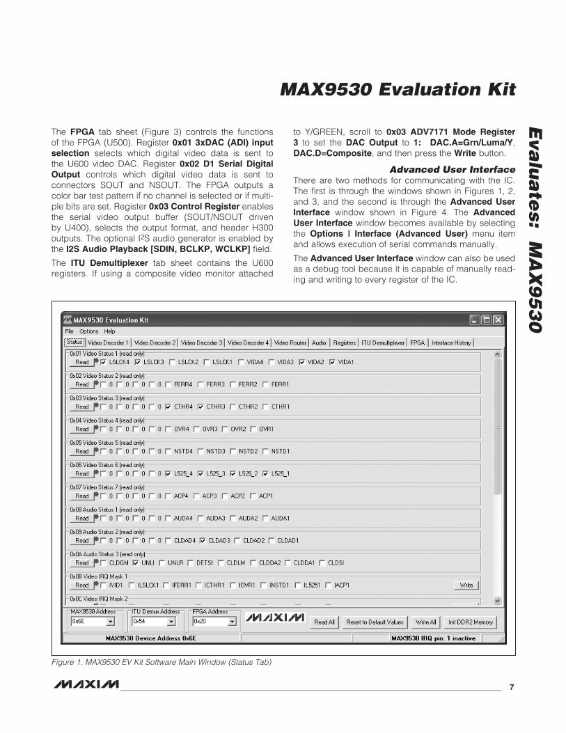
8) Color Bar Test: On the Video Decoder 1 tab sheet, scroll down to register 0x2B Test Pattern and set CBAR to 10: 75% Color Bars. Press the Writebutton. The video display shows 75% color bars.
9) Quad Splitscreen Test (NTSC): Configure a unique video signal for each of the four video inputs.
10) Select File | Load Configuration File… inside the config_files folder, and load file max9530_scale-360-525_ovl.MAX9530. The video display shows video signal 1 scaled to fit into the upper quadrant of the screen, and the rest of the video display is blank.
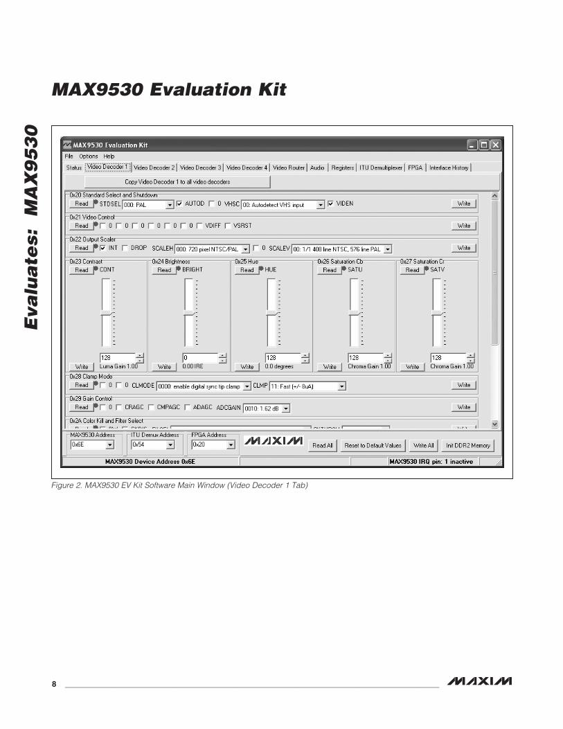
11) On the FPGA tab sheet, inside the 0x01 3xDAC (ADI) input selection group box, check four channel overlay and remove the checks from chan-nel 4 through channel 1. The video display is recon-figured to show a split screen with four images from each of the four video decoders.
12) On the Video Router tab sheet, scroll to register 0x60 FIFO Source and change the order from Vin4 – Vin3 – Vin2 – Vin1 and press the Write button. The new order is reflected in the video display. The channel selected by CH1R appears in the upper-left quadrant of the video display.
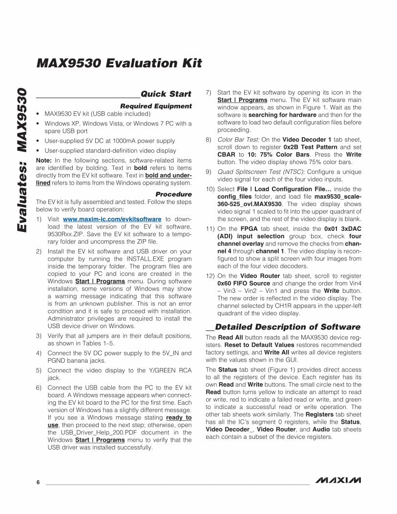
Detailed Description of SoftwareThe Read All button reads all the MAX9530 device reg-isters. Reset to Default Values restores recommended factory settings, and Write All writes all device registers with the values shown in the GUI.
The Status tab sheet (Figure 1) provides direct access to all the registers of the device. Each register has its own Read and Write buttons. The small circle next to the Read button turns yellow to indicate an attempt to read or write, red to indicate a failed read or write, and green to indicate a successful read or write operation. The other tab sheets work similarly. The Registers tab sheet has all the IC’s segment 0 registers, while the Status, Video Decoder_, Video Router, and Audio tab sheets each contain a subset of the device registers.
MAX9530 Evaluation Kit
Eva
lua
tes: M
AX
95
30
_______________________________________________________________________________________ 7
The FPGA tab sheet (Figure 3) controls the functions of the FPGA (U500). Register 0x01 3xDAC (ADI) input selection selects which digital video data is sent to the U600 video DAC. Register 0x02 D1 Serial Digital Output controls which digital video data is sent toconnectors SOUT and NSOUT. The FPGA outputs a color bar test pattern if no channel is selected or if multi-ple bits are set. Register 0x03 Control Register enables the serial video output buffer (SOUT/NSOUT driven by U400), selects the output format, and header H300 outputs. The optional I2S audio generator is enabled by the I2S Audio Playback [SDIN, BCLKP, WCLKP] field.
The ITU Demultiplexer tab sheet contains the U600 registers. If using a composite video monitor attached
to Y/GREEN, scroll to 0x03 ADV7171 Mode Register 3 to set the DAC Output to 1: DAC.A=Grn/Luma/Y, DAC.D=Composite, and then press the Write button.
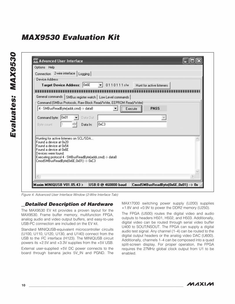
Advanced User InterfaceThere are two methods for communicating with the IC. The first is through the windows shown in Figures 1, 2, and 3, and the second is through the Advanced User Interface window shown in Figure 4. The Advanced User Interface window becomes available by selecting the Options | Interface (Advanced User) menu item and allows execution of serial commands manually.
The Advanced User Interface window can also be used as a debug tool because it is capable of manually read-ing and writing to every register of the IC.
Figure 1. MAX9530 EV Kit Software Main Window (Status Tab)
MAX9530 Evaluation Kit
Eva
lua
tes:
M
AX
95
30
8 ______________________________________________________________________________________
Figure 2. MAX9530 EV Kit Software Main Window (Video Decoder 1 Tab)
MAX9530 Evaluation Kit
Eva
lua
tes: M
AX
95
30
_______________________________________________________________________________________ 9
Figure 3. MAX9530 EV Kit Software Main Window (FPGA Tab)
MAX9530 Evaluation Kit
Eva
lua
tes:
M
AX
95
30
10 _____________________________________________________________________________________
Figure 4. Advanced User Interface Window (2-Wire Interface Tab)
Detailed Description of HardwareThe MAX9530 EV kit provides a proven layout for the MAX9530. Frame buffer memory, multifunction FPGA, analog audio and video output buffers, and easy-to-use USB-PC connection are included on the EV kit.
Standard MINIQUSB-equivalent microcontroller circuits (U100, U110, U120, U130, and U140) connect from the USB to the I2C interface (H123). The MINIQUSB circuit powers its +2.5V and +3.3V supplies from the +5V USB.
External user-supplied +5V DC power connects to the board through banana jacks 5V_IN and PGND. The
MAX17000 switching power supply (U200) supplies +1.8V and +0.9V to power the DDR2 memory (U250).
The FPGA (U500) routes the digital video and audio outputs to headers H501, H502, and H503. Additionally, digital video can be routed through serial video buffer U400 to SOUT/NSOUT. The FPGA can supply a digital audio test signal. Any channel (1–4) can be routed to the digital output headers or the analog video DAC (U600). Additionally, channels 1–4 can be composed into a quad split-screen display. For proper operation, the FPGA requires the 27MHz global clock output from U1 to be enabled.
MAX9530 Evaluation Kit
Eva
lua
tes: M
AX
95
30
______________________________________________________________________________________ 11
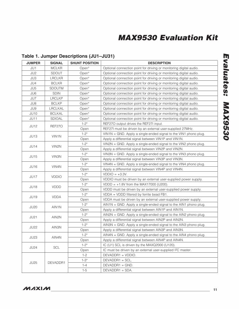
Table 1. Jumper Descriptions (JU1–JU31)JUMPER SIGNAL SHUNT POSITION DESCRIPTION
JU1 MCLKR Open* Optional connection point for driving or monitoring digital audio.
JU2 SDOUT Open* Optional connection point for driving or monitoring digital audio.
JU3 LRCLKR Open* Optional connection point for driving or monitoring digital audio.
JU4 BCLKR Open* Optional connection point for driving or monitoring digital audio.
JU5 SDOUTM Open* Optional connection point for driving or monitoring digital audio.
JU6 SDIN Open* Optional connection point for driving or monitoring digital audio.
JU7 LRCLKP Open* Optional connection point for driving or monitoring digital audio.
JU8 BCLKP Open* Optional connection point for driving or monitoring digital audio.
JU9 LRCLKAL Open* Optional connection point for driving or monitoring digital audio.
JU10 BCLKAL Open* Optional connection point for driving or monitoring digital audio.
JU11 SDIOAL Open* Optional connection point for driving or monitoring digital audio.
JU12 REF27O1-2* REF27O output drives the REF27I input.
Open REF27I must be driven by an external user-supplied 27MHz.
JU13 VIN1N1-2* VIN1N = GND. Apply a single-ended signal to the VIN1 phono plug.
Open Apply a differential signal between VIN1P and VIN1N.
JU14 VIN2N1-2* VIN2N = GND. Apply a single-ended signal to the VIN2 phono plug.
Open Apply a differential signal between VIN2P and VIN2N.
JU15 VIN3N1-2* VIN3N = GND. Apply a single-ended signal to the VIN3 phono plug.
Open Apply a differential signal between VIN3P and VIN3N.
JU16 VIN4N1-2* VIN4N = GND. Apply a single-ended signal to the VIN4 phono plug.
Open Apply a differential signal between VIN4P and VIN4N.
JU17 VDDIO1-2* VDDIO = +3.3V.
Open VDDIO must be driven by an external user-supplied power supply.
JU18 VDDD1-2* VDDD = +1.8V from the MAX17000 (U200).
Open VDDD must be driven by an external user-supplied power supply.
JU19 VDDA1-2* VDDA = VDDD filtered by ferrite bead FB1.
Open VDDA must be driven by an external user-supplied power supply.
JU20 AIN1N1-2* AIN1N = GND. Apply a single-ended signal to the AIN1 phono plug.
Open Apply a differential signal between AIN1P and AIN1N.
JU21 AIN2N1-2* AIN2N = GND. Apply a single-ended signal to the AIN2 phono plug.
Open Apply a differential signal between AIN2P and AIN2N.
JU22 AIN3N1-2* AIN3N = GND. Apply a single-ended signal to the AIN3 phono plug.
Open Apply a differential signal between AIN3P and AIN3N.
JU23 AIN4N1-2* AIN4N = GND. Apply a single-ended signal to the AIN4 phono plug.
Open Apply a differential signal between AIN4P and AIN4N.
JU24 SCL1-2* IC (U1) SCL is driven by the MAXQ2000 (U120).
Open IC must be driven by an external user-supplied I2C master.
JU25 DEVADDR1
1-2 DEVADDR1 = VDDIO.
1-3* DEVADDR1 = SCL.
1-4 DEVADDR1 = GND.
1-5 DEVADDR1 = SDA.

MAX9530 Evaluation Kit
Eva
lua
tes:
M
AX
95
30
12 _____________________________________________________________________________________
Table 1. Jumper Descriptions (JU1–JU31) (continued)
Table 2. Jumper Descriptions (JU201–JU209)
*Default position.
JUMPER SIGNAL SHUNT POSITION DESCRIPTION
JU26 SDA1-2* IC (U1) SDA is driven by the MAXQ2000 (U120).
Open IC must be driven by an external user-supplied I2C master.
JU27 SCL pullup1-2* R66 pulls up idle SCL to VDDIO.
Open SCL requires an external user-supplied resistive pullup.
JU28 SDA pullup1-2* R67 pulls up idle SDA to VDDIO.
Open SDA requires an external user-supplied resistive pullup.
JU29 IRQB1-2* IC (U1) IRQB drives the MAXQ2000 (U120) on the MINIQUSB GPIO pin K1.
Open Connect IC (U1) IRQB to user-supplied controller.
JU30 RSTB1-2*
IC (U1) RSTB is driven by the MAXQ2000 (U120) from the MINIQUSB GPIO pin K2.
Open Drive IC (U1) RSTB from a user-supplied controller.
JU31 DEVADDR0
1-2 DEVADDR0 = VDDIO.
1-3* DEVADDR0 = SCL.
1-4 DEVADDR0 = GND.
1-5 DEVADDR0 = SDA.
JUMPER SIGNAL SHUNT POSITION DESCRIPTION
JU201 U200 OVP1-2 MAX17000 (U200) OVP = AGND. Overvoltage protection is disabled.
Open* MAX17000 (U200) OVP = VDD. Overvoltage protection is enabled.
JU202 U200 FB
1-2* MAX17000 (U200) FB connects to VDD. VOUT = +1.8V.
2-3 MAX17000 (U200) FB connects to GND. VOUT = +1.5V.
OpenMAX17000 (U200) FB connects to resistive-dividers R214/R215. Refer to the MAX17000 IC data sheet.
JU203U200 STDBY
1-2 MAX17000 (U200) STDBY = GND. VTT is disabled (U250 DDR2 memory not powered).
Open* MAX17000 (U200) STDBY = VDD. VTT = +0.9V. Normal operation of DDR2 memory.
JU204 U200 SKIP
1-2 MAX17000 (U200) SKIP = GND. Pulse-skipping mode is enabled.
Open* MAX17000 (U200) SKIP = VDD. Forced-PWM operation mode, no pulse-skipping.
JU205 U200 SHDN
1-2 MAX17000 (U200) SHDN = GND. VOUT is disabled (U250 DDR2 memory is not powered).
Open* MAX17000 (U200) SHDN = VDD. VOUT = +1.8V. Normal operation of DDR2 memory.
JU206 U200 REFIN1-2* MAX17000 (U200) REFIN = VDD. VTT = VCSL/2.
Open Refer to the MAX17000 IC data sheet.
MAX9530 Evaluation Kit
Eva
lua
tes: M
AX
95
30
______________________________________________________________________________________ 13
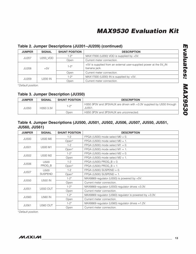
Table 2. Jumper Descriptions (JU201–JU209) (continued)
Table 3. Jumper Description (JU350)
Table 4. Jumper Descriptions (JU500, JU501, JU502, JU506, JU507, JU550, JU551, JU560, JU561)
*Default position.
*Default position.
JUMPER SIGNAL SHUNT POSITION DESCRIPTION
JU207 U200_VDD1-2* MAX17000 (U200) VDD is supplied by +5V.
Open Current meter connection.
JU208 +5V1-2*
+5V is supplied from an external user-supplied power at the 5V_IN banana jack.
Open Current meter connection.
JU209 U200 IN1-2* MAX17000 (U200) IN is supplied by +5V.
Open Current meter connection.
JUMPER SIGNAL SHUNT POSITION DESCRIPTION
JU350 H350 3.3V1-2*
H350 3P3V and 3P3VAUX are driven with +3.3V supplied by U550 through JU551.
Open H350 3P3V and 3P3VAUX are unconnected.
JUMPER SIGNAL SHUNT POSITION DESCRIPTION
JU500 U500 M01-2 FPGA (U500) mode select M0 = 0.
Open* FPGA (U500) mode select M0 = 1.
JU501 U500 M11-2 FPGA (U500) mode select M1 = 0.
Open* FPGA (U500) mode select M1 = 1.
JU502 U500 M21-2* FPGA (U500) mode select M2 = 0.
Open FPGA (U500) mode select M2 = 1.
JU506U500
PROG_B1-2 FPGA (U500) PROG_B = 0.
Open* FPGA (U500) PROG_B = 1.
JU507U500
SUSPEND1-2 FPGA (U500) SUSPEND = 0.
Open* FPGA (U500) SUSPEND = 1.
JU550 U550 IN1-2* MAX8869 regulator (U550) is powered by +5V.
Open Current meter connection.
JU551 U550 OUT1-2* MAX8869 regulator (U550) regulator drives +3.3V.
Open Current meter connection.
JU560 U560 IN1-2* MAX8869 regulator (U560) regulator is powered by +3.3V.
Open Current meter connection.
JU561 U560 OUT1-2* MAX8869 regulator (U560) regulator drives +1.2V.
Open Current meter connection.
MAX9530 Evaluation Kit
Eva
lua
tes:
M
AX
95
30
14 _____________________________________________________________________________________
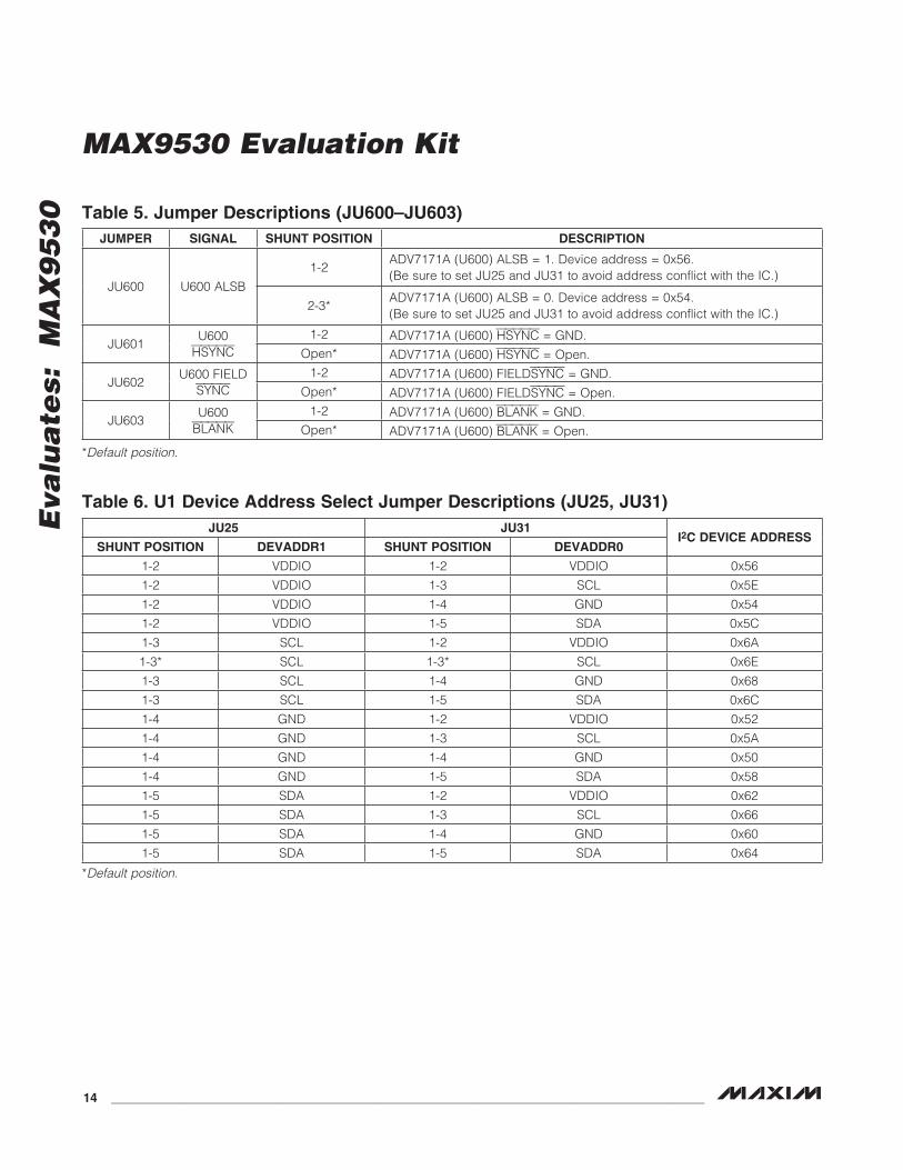
Table 5. Jumper Descriptions (JU600–JU603)
Table 6. U1 Device Address Select Jumper Descriptions (JU25, JU31)
*Default position.
*Default position.
JUMPER SIGNAL SHUNT POSITION DESCRIPTION
JU600 U600 ALSB
1-2ADV7171A (U600) ALSB = 1. Device address = 0x56. (Be sure to set JU25 and JU31 to avoid address conflict with the IC.)
2-3*ADV7171A (U600) ALSB = 0. Device address = 0x54. (Be sure to set JU25 and JU31 to avoid address conflict with the IC.)
JU601U600 HSYNC
1-2 ADV7171A (U600) HSYNC = GND.Open* ADV7171A (U600) HSYNC = Open.
JU602U600 FIELD
SYNC1-2 ADV7171A (U600) FIELDSYNC = GND.
Open* ADV7171A (U600) FIELDSYNC = Open.
JU603U600 BLANK
1-2 ADV7171A (U600) BLANK = GND.Open* ADV7171A (U600) BLANK = Open.
JU25 JU31I2C DEVICE ADDRESS
SHUNT POSITION DEVADDR1 SHUNT POSITION DEVADDR0
1-2 VDDIO 1-2 VDDIO 0x56
1-2 VDDIO 1-3 SCL 0x5E
1-2 VDDIO 1-4 GND 0x54
1-2 VDDIO 1-5 SDA 0x5C
1-3 SCL 1-2 VDDIO 0x6A
1-3* SCL 1-3* SCL 0x6E
1-3 SCL 1-4 GND 0x68
1-3 SCL 1-5 SDA 0x6C
1-4 GND 1-2 VDDIO 0x52
1-4 GND 1-3 SCL 0x5A
1-4 GND 1-4 GND 0x50
1-4 GND 1-5 SDA 0x58
1-5 SDA 1-2 VDDIO 0x62
1-5 SDA 1-3 SCL 0x66
1-5 SDA 1-4 GND 0x60
1-5 SDA 1-5 SDA 0x64
MAX9530 Evaluation Kit
Eva
lua
tes: M
AX
95
30
______________________________________________________________________________________ 15
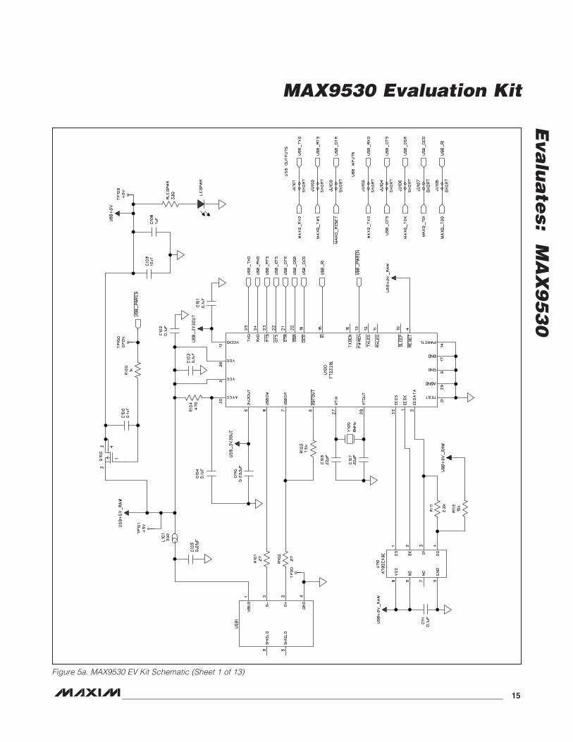
Figure 5a. MAX9530 EV Kit Schematic (Sheet 1 of 13)
MAX9530 Evaluation Kit
Eva
lua
tes:
M
AX
95
30
16 _____________________________________________________________________________________
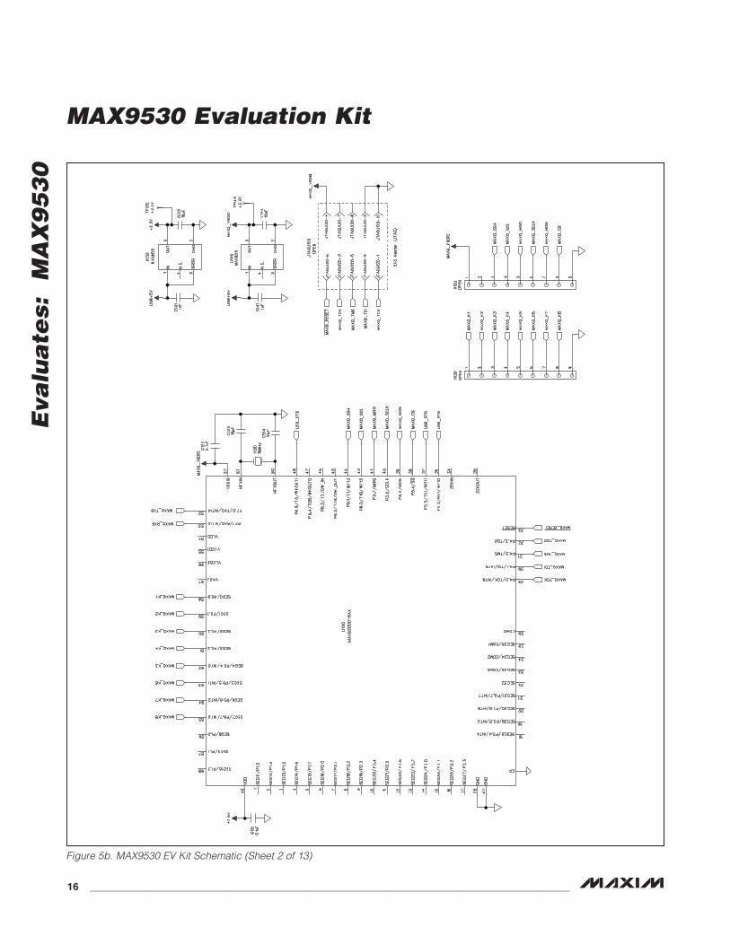
Figure 5b. MAX9530 EV Kit Schematic (Sheet 2 of 13)
MAX9530 Evaluation Kit
Eva
lua
tes: M
AX
95
30
______________________________________________________________________________________ 17
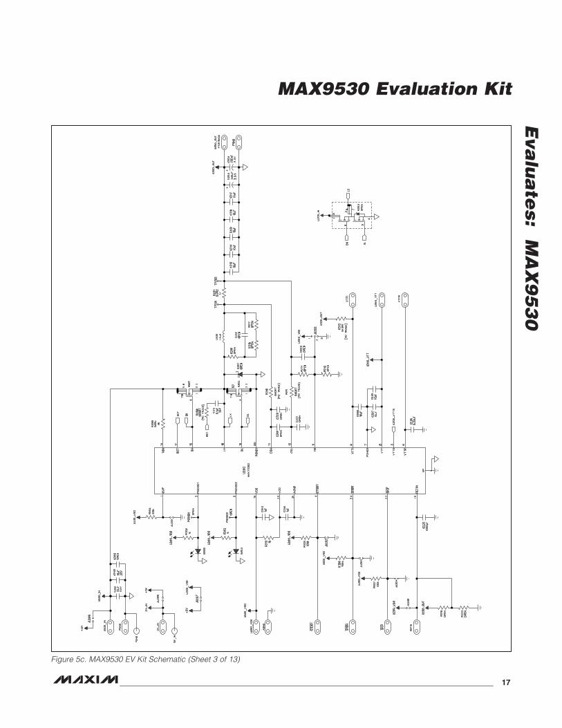
Figure 5c. MAX9530 EV Kit Schematic (Sheet 3 of 13)

MAX9530 Evaluation Kit
Eva
lua
tes:
M
AX
95
30
18 _____________________________________________________________________________________
Figure 5d. MAX9530 EV Kit Schematic (Sheet 4 of 13)
MAX9530 Evaluation Kit
Eva
lua
tes: M
AX
95
30
______________________________________________________________________________________ 19
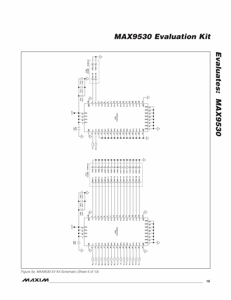
Figure 5e. MAX9530 EV Kit Schematic (Sheet 5 of 13)

MAX9530 Evaluation Kit
Eva
lua
tes:
M
AX
95
30
20 _____________________________________________________________________________________
Figure 5f. MAX9530 EV Kit Schematic (Sheet 6 of 13)
MAX9530 Evaluation Kit
Eva
lua
tes: M
AX
95
30
______________________________________________________________________________________ 21
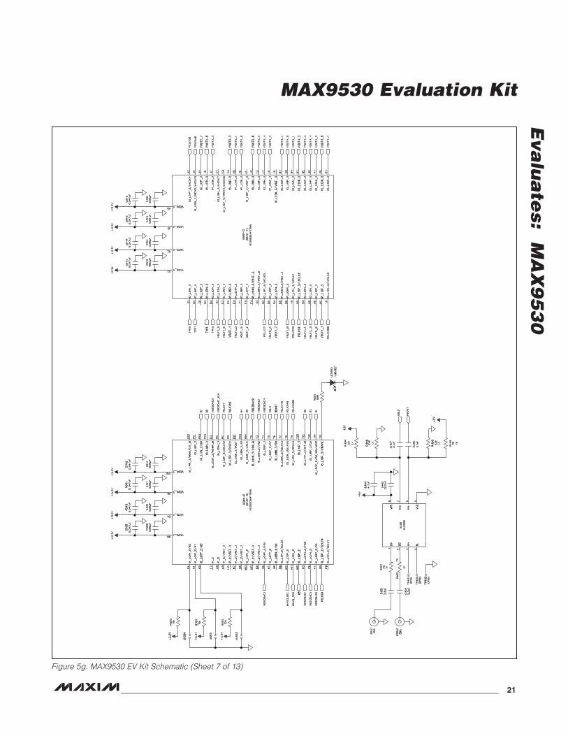
Figure 5g. MAX9530 EV Kit Schematic (Sheet 7 of 13)
MAX9530 Evaluation Kit
Eva
lua
tes:
M
AX
95
30
22 _____________________________________________________________________________________
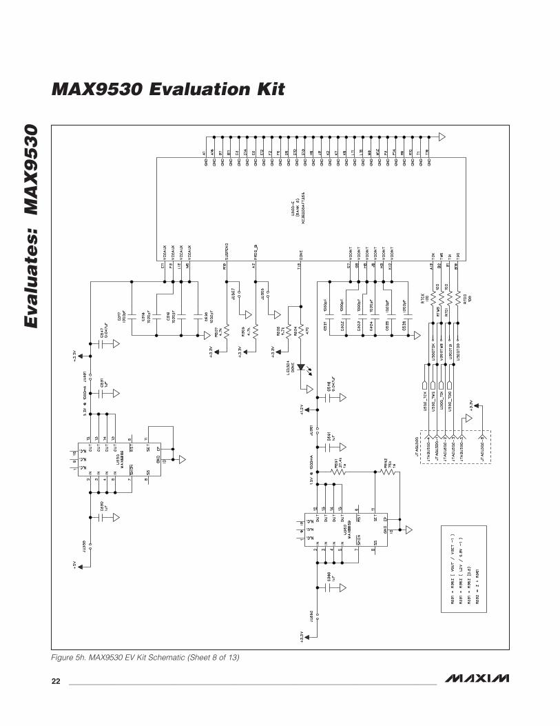
Figure 5h. MAX9530 EV Kit Schematic (Sheet 8 of 13)
MAX9530 Evaluation Kit
Eva
lua
tes: M
AX
95
30
______________________________________________________________________________________ 23
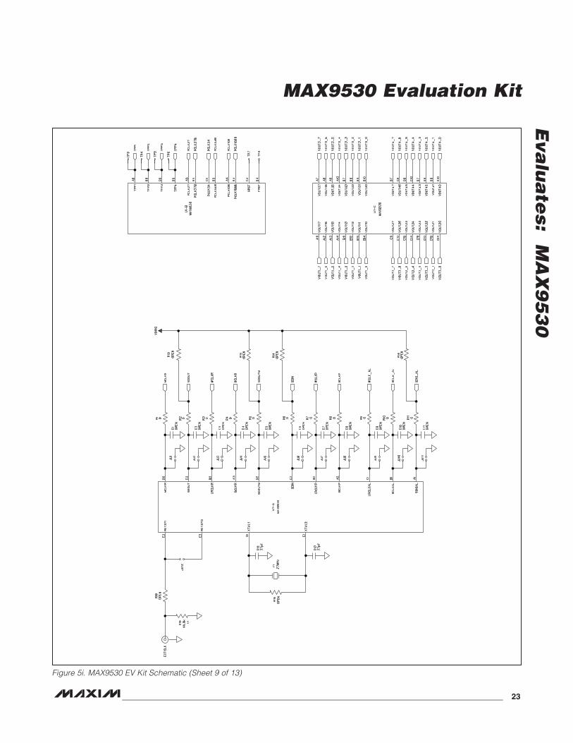
Figure 5i. MAX9530 EV Kit Schematic (Sheet 9 of 13)
MAX9530 Evaluation Kit
Eva
lua
tes:
M
AX
95
30
24 _____________________________________________________________________________________
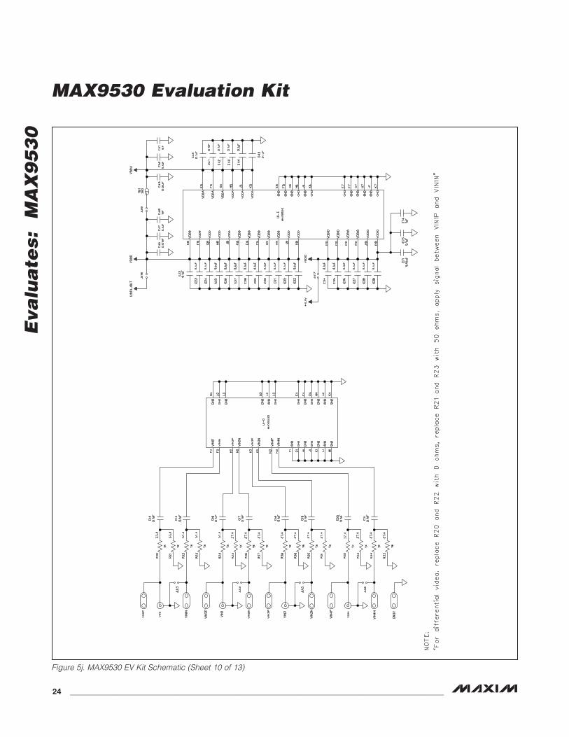
Figure 5j. MAX9530 EV Kit Schematic (Sheet 10 of 13)
MAX9530 Evaluation Kit
Eva
lua
tes: M
AX
95
30
______________________________________________________________________________________ 25
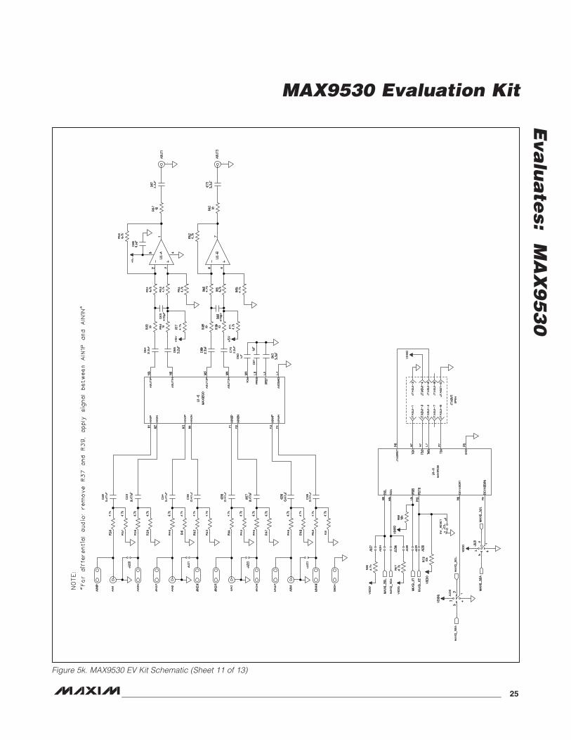
Figure 5k. MAX9530 EV Kit Schematic (Sheet 11 of 13)
MAX9530 Evaluation Kit
Eva
lua
tes:
M
AX
95
30
26 _____________________________________________________________________________________
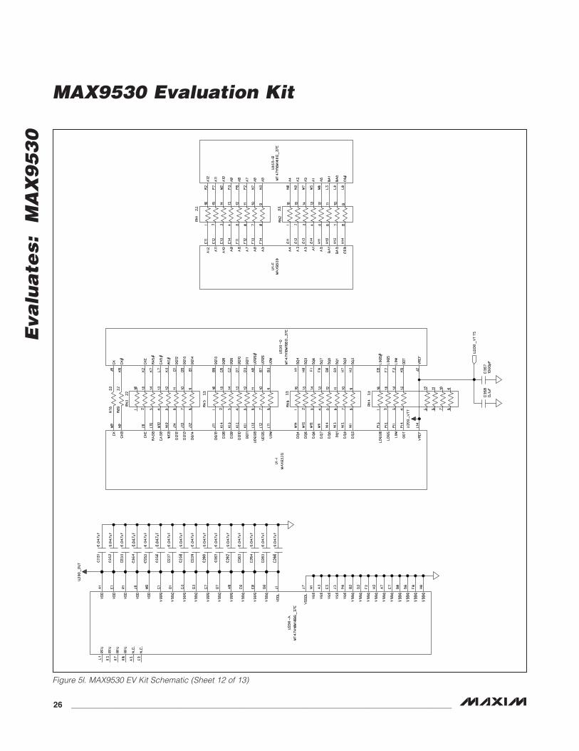
Figure 5l. MAX9530 EV Kit Schematic (Sheet 12 of 13)
MAX9530 Evaluation Kit
Eva
lua
tes: M
AX
95
30
______________________________________________________________________________________ 27
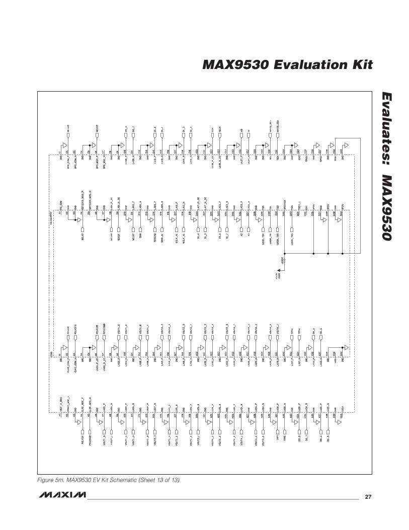
Figure 5m. MAX9530 EV Kit Schematic (Sheet 13 of 13)
MAX9530 Evaluation Kit
Eva
lua
tes:
M
AX
95
30
28 _____________________________________________________________________________________
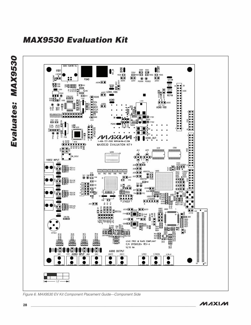
Figure 6. MAX9530 EV Kit Component Placement Guide—Component Side
1.0”
MAX9530 Evaluation Kit
Eva
lua
tes: M
AX
95
30
______________________________________________________________________________________ 29
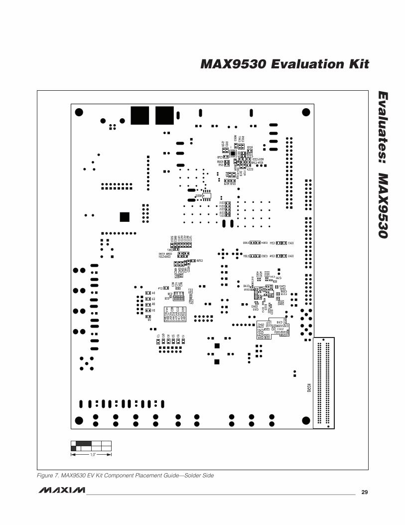
Figure 7. MAX9530 EV Kit Component Placement Guide—Solder Side
1.0”
MAX9530 Evaluation Kit
Eva
lua
tes:
M
AX
95
30
30 _____________________________________________________________________________________
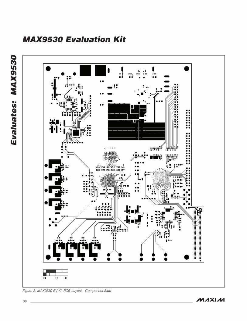
Figure 8. MAX9530 EV Kit PCB Layout—Component Side
1.0”
MAX9530 Evaluation Kit
Eva
lua
tes: M
AX
95
30
______________________________________________________________________________________ 31
Figure 9. MAX9530 EV Kit PCB Layout—Ground Layer 2
1.0”
MAX9530 Evaluation Kit
Eva
lua
tes:
M
AX
95
30
32 _____________________________________________________________________________________
Figure 10. MAX9530 EV Kit PCB Layout—Power Layer 3
1.0”
MAX9530 Evaluation Kit
Eva
lua
tes: M
AX
95
30
______________________________________________________________________________________ 33
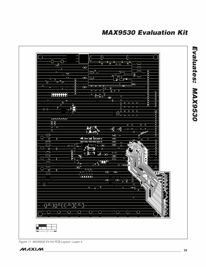
Figure 11. MAX9530 EV Kit PCB Layout—Layer 4
1.0”
MAX9530 Evaluation Kit
Eva
lua
tes:
M
AX
95
30
34 _____________________________________________________________________________________
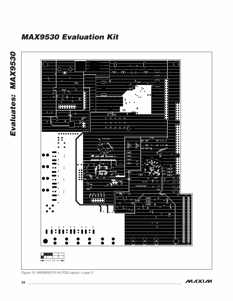
Figure 12. MAX9530 EV Kit PCB Layout—Layer 5
1.0”
MAX9530 Evaluation Kit
Eva
lua
tes: M
AX
95
30
______________________________________________________________________________________ 35
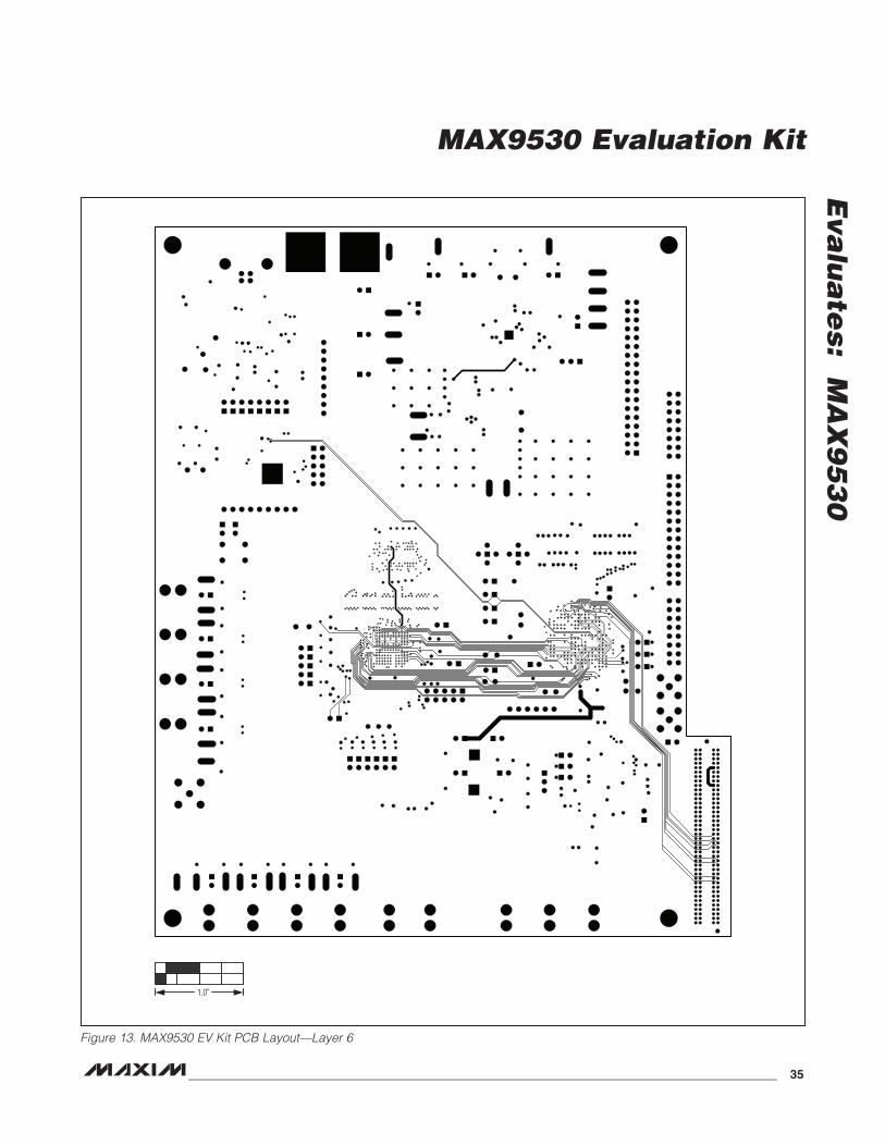
Figure 13. MAX9530 EV Kit PCB Layout—Layer 6
1.0”
MAX9530 Evaluation Kit
Eva
lua
tes:
M
AX
95
30
36 _____________________________________________________________________________________
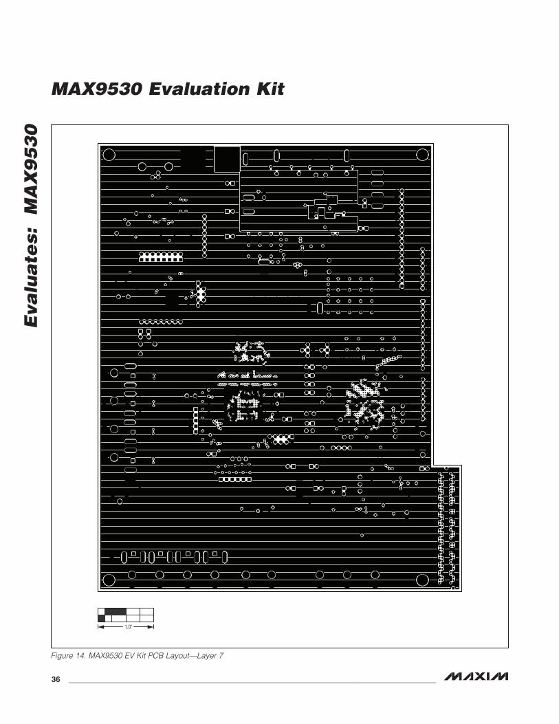
Figure 14. MAX9530 EV Kit PCB Layout—Layer 7
1.0”
MAX9530 Evaluation Kit
Eva
lua
tes: M
AX
95
30
______________________________________________________________________________________ 37
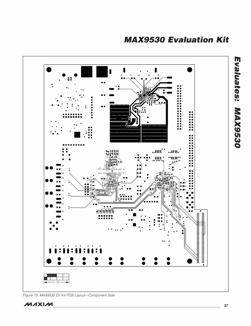
Figure 15. MAX9530 EV Kit PCB Layout—Component Side
1.0”
Maxim cannot assume responsibility for use of any circuitry other than circuitry entirely embodied in a Maxim product. No circuit patent licenses are implied. Maxim reserves the right to change the circuitry and specifications without notice at any time.
38 Maxim Integrated Products, 120 San Gabriel Drive, Sunnyvale, CA 94086 408-737-7600© 2010 Maxim Integrated Products Maxim is a registered trademark of Maxim Integrated Products, Inc.
MAX9530 Evaluation Kit
Eva
lua
tes:
M
AX
95
30 Revision History
REVISIONNUMBER
REVISION DATE
DESCRIPTIONPAGES
CHANGED
0 12/10 Initial release —