Embed Size (px)
Citation preview

NFE-11-03200
Page 1 of 20
Material Science & Technology Division
CRADA Final Report For
CRADA Number NFE-11-03200
Wide Area Thermal Processing of Light Emitting Materials
Chad Duty, PhD Oak Ridge National Laboratory
Nathaniel Quick, PhD AppliCote Associates, LLC
Prepared by Oak Ridge National Laboratory
Oak Ridge, TN 37831 Managed by
UT-BATELLE, LLC for the
U.S. Department of Energy Under contract DE-AC05-00OR22725
Approved for Public Release
NFE-11-03200
Page 2 of 20

NFE-11-03200
Page 3 of 20
Table of Contents
Executive Summary .................................................................................................................... 4 Project Objective ........................................................................................................................... 5
Modeling ....................................................................................................................................... 6 SiC-‐4H: Material Properties ...................................................................................................... 8 Resistivity/Hall Effect ............................................................................................................... 8 Transmission ............................................................................................................................. 8 Ellipsometry ............................................................................................................................... 9 Photoluminescence ................................................................................................................... 9 Discussion ................................................................................................................................ 10
Laser Annealing Experiments ................................................................................................ 11
PTP Processing .......................................................................................................................... 12 Impact of PulseForge Annealing ............................................................................................ 13 Impact of Vortek 300 Processing ........................................................................................... 13 Process Range ....................................................................................................................... 13 Surface Morphology ............................................................................................................. 13 XPS Analysis .......................................................................................................................... 14 Electrical Performance ........................................................................................................ 16
Summary and Direction ........................................................................................................... 17 Task Schedule .............................................................................................................................. 18
Spending Schedule .................................................................................................................... 19 Cost Share Contributions ........................................................................................................... 20
NFE-11-03200
Page 4 of 20
Executive Summary Silicon carbide based materials and devices have been successfully exploited for diverse electronic applications. However, they have not achieved the same success as Si technologies due to higher material cost and higher processing temperatures required for device development. Traditionally, SiC is not considered for optoelectronic applications because it has an indirect bandgap. However, AppliCote Associates, LLC has developed a laser-based doping process which enables light emission in SiC through the creation of embedded p-n junctions. AppliCote laser irradiation of silicon carbide allows two different interaction mechanisms:
1. Laser conversion or induced phase transformation which creates carbon rich regions that have conductive properties. These conductive regions are required for interconnection to the light emitting semiconducting region.
2. Laser doping which injects external dopant atoms into the substrate that introduces deep level transition states that emit light when electrically excited.
The current collaboration with AppliCote has focused on the evaluation of ORNL’s unique Pulse Thermal Processing (PTP) technique as a replacement for laser processing. Compared to laser processing, Pulse Thermal Processing can deliver similar energy intensities (20-50 kW/cm2) over a much larger area (up to 1,000 cm2) at a lower cost and much higher throughput. The main findings of our investigation; which are significant for the realization of SiC based optoelectronic devices, are as follows:
• The PTP technique is effective in low thermal budget activation of dopants in SiC similar to the laser technique. The surface electrical conductivity of the SiC samples improved by about three orders of magnitude as a result of PTP processing which is significant for charge injection in the devices.
• The surface composition of the SiC film can be modified by the PTP technique to create a carbon-rich surface (increased local C:Si ratio from 1:1 to 2.9:1). This is significant as higher thermal and electrical conductivities of the surface layer are critical for a successful development of integrated optoelectronic devices.
• PTP provides low thermal budget dopant activation with a controlled depth profile, which can be exploited for high performance device development with selective patterning of the substrate.
This project has successfully demonstrated that a low thermal budget annealing technique, such as PTP, is critical to defining the path for low cost electronic devices integrated on glass or polymeric substrates. This project is complimentary to the goals of the Solid State Lighting Program within DOE. It involves new manufacturing techniques for light emitting materials that are potentially much lower cost and energy efficient than existing products. Significant opportunity exists for further exploration of AppliCote’s material and device technology in combination with ORNL’s PTP technique, modeling, and characterization capabilities.
NFE-11-03200
Page 5 of 20
Project Objective Laser-based synthesis of wide bandgap materials has been successfully used to create white light emitting materials (LEMs). This technology development has progressed to the exploration on design and construction of apparatus for wide area doping and phase transformation of wide bandgap material substrates. The objective of this proposal is to develop concepts for wide area doping and phase transformation based on AppliCote Associates, LLC laser technology and ORNL high density pulsed plasma arc technology. Background: AppliCote Associates, LLC has developed a Laser Materials Synthesis process which produces Light Emitting Material that can be used in lighting applications with greater efficiency, significantly lower environmental impacts, and a broader array of applications than compact florescent and LED technologies. The specific laser processing tools and devices utilized in LMS are patented with additional patents filed on improvements to the process.
An advance over traditional LED technology is that light emitting materials emit white light over a large surface area, thus eliminating the need for point light source array assemblies and complex device packaging. This technology has been developed by AppliCote Associates, LLC team using laser processing, particularly laser conversion and laser doping. Efforts are in progress to expand the laser beam size and beam translation technologies to approach wide area processing. Currently a beam diameter of 1.4 cm is used and it is proposed that this beam be rastered by galvo mirror mechanisms or across a substrate using a laser gas assist nozzle design to discharge and evacuate doping gases eliminating the need for chambers.
ORNL has developed the Pulse Thermal Processing (PTP) technology based on high density pulsed plasma arc lamps that can provide heating and cooling rates on the order of 6 x 10⁵ °C/s, temperatures on the order of 3000°C, and wide area processing (up to 1,000 cm2). While the temperature is sufficient to drive solid state diffusion in wide bandgap materials, modeling and research must be conducted to determine if the 6 x 10⁵ °C/s heating/cooling rate is sufficient to create the chemistries and nanostructures necessary for light emission or if additional apparatus research and design is required to boost pulsed plasma arc heating and cooling rates or if the substrate materials must be selected or designed to improve their thermal conductivity as an assist for rapid cooling.
Commercialization Status: There was no activity toward commercialization at this stage of development. Invention Disclosures: None to date.
Patents: None to date. Publications / Presentations: None to date.
NFE-11-03200
Page 6 of 20
Modeling Extensive modeling of the laser doping process was conducted at AppliCote Associates. Initially the intent was to match the following laser parameters for nitrogen in available n-type SiC substrates. A boost in nitrogen concentration was anticipated in these substrates already containing nitrogen (commercial grade material). In a Phase II CRADA p-type-SiC substrates will be special ordered for easier discrimination of nitrogen doping.
Table 1. Nd:YAG (1064 nm) laser doping process parameters for SiC LED fabrication.
The goal is to predict the dopant mass flux injected into the substrate by a set of chosen laser processing parameters. We are using the dopant mass flux as opposed to just as a function of laser processing parameters rather than concentration profile as a function of laser processing parameters so that we can evaluate and understand the laser electromagnetic field effects on the laser doping process. This predictive capability will evolve into a laser doping process control. The first path is to simplify the total dopant mass flux equation so that it varies with laser irradiance incident on the wafer’s surface (Iu ). The principle reference used in this approach is Sachin Bet “Laser enhanced Doping for Silicon Carbide White Light Emitting Diode”, University of Central Florida, 2008. This thesis was in part supported by AppliCote Associates, LLC. Elements of the approach are as follows: 1. Consider the total mass flux of dopant atoms that is injected into the substrate (e.g., SiC).
This flux is defined by1: 1 Sachin Bet, “Laser enhanced Doping for Silicon Carbide White Light Emitting Diode”, Ph. D. Thesis, University of Central Florida, 2008.
Dopant Power (W)
Pulse Repetition
Rate (KHz)
Focal Length (mm)
Spot Size (µm)
No. of Passes
Scanning Speed
(mm/sec)
Dopant Medium
p-type
(deferred)
Al 11.5-12
5 150 65 2 0.5 Trimethyl aluminum, Methane
30psi
p-type
(deferred)
Cr 12.5-13
5 150 65 1 0.5 Bis (ethyl benzene)-chromium,
argon 30 psi
n-type
(studied)
N 12 5 150 80 3 0.8 Ultra high pure nitrogen
30psi
n-type
(deferred)
Se 11.5-13
5 150 100 2 0.8 Diethyl selenium,
argon 30 psi
NFE-11-03200
Page 7 of 20
( ) ( ) ⎥⎦
⎤Δ++⎢
⎣
⎡+
∂
∂−=
),()),((,)),(1(,
),()),((),()),((
tzTktzTDEtzCAtzTeEtzC
tzTktzTD
ztzCtzTDJ
BYsel
B
α a)
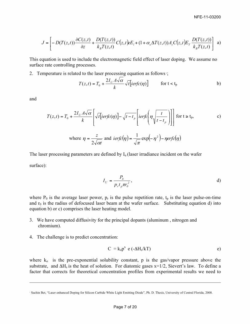
This equation is used to include the electromagnetic field effect of laser doping. We assume no surface rate controlling processes.
2. Temperature is related to the laser processing equation as follows 2;
[ ])(2),( 0 η
α ierfctkAITtzT U+= for t < tp b)
and
[ ]⎥⎥
⎦
⎤
⎢⎢
⎣
⎡
⎥⎥⎦
⎤
⎢⎢⎣
⎡
⎟⎟
⎠
⎞
⎜⎜
⎝
⎛
−−−+=
pp
U
tttierfcttierfct
kAI
TtzT ηηα
)(2
),( 0 for t ≥ tp, c)
where t
zα
η2
= and ( ) ( ) ( )ηηηπ
η erfcierfc −−= 2exp1
The laser processing parameters are defined by Iu (laser irradiance incident on the wafer
surface):
20pr
0U πrtp
PI = , d)
where P0 is the average laser power, pr is the pulse repetition rate, tp is the laser pulse-on-time and r0 is the radius of defocused laser beam at the wafer surface. Substituting equation d) into equation b) or c) comprises the laser heating model. 3. We have computed diffusivity for the principal dopants (aluminum , nitrogen and
chromium).
4. The challenge is to predict concentration:
C = kopx e (-ΔHs/kT) e) where ko is the pre-exponential solubility constant, p is the gas/vapor pressure above the substrate, and ΔHs is the heat of solution. For diatomic gases x=1/2, Sievert’s law. To define a factor that corrects for theoretical concentration profiles from experimental results we need to
2 Sachin Bet, “Laser enhanced Doping for Silicon Carbide White Light Emitting Diode”, Ph. D. Thesis, University of Central Florida, 2008.
NFE-11-03200
Page 8 of 20
plot the theoretical predictions against secondary ion mass spectroscopy (SIMS) concentration profiles. Any other instrument that determines dopant concentration profiles can also be used if available. 5. The final step is to make appropriate substitutions e.g., d into b or c, b or c into a, e into a)
into the mass flux equation and simplify. 6. An alternate and simpler approach once the effect of laser electromagnetic field effect is
understood is to evaluate dopant concentration as a function of temperature and hence laser processing parameters. Here the substitutions are d into b or c, b or c into e.
7. Ultimately we would like to predict dopant concentration profile as a function of the laser process parameters.
8. These paths are a starting point for discussion. Sections 2 and 3 form the basis for these and other approaches.
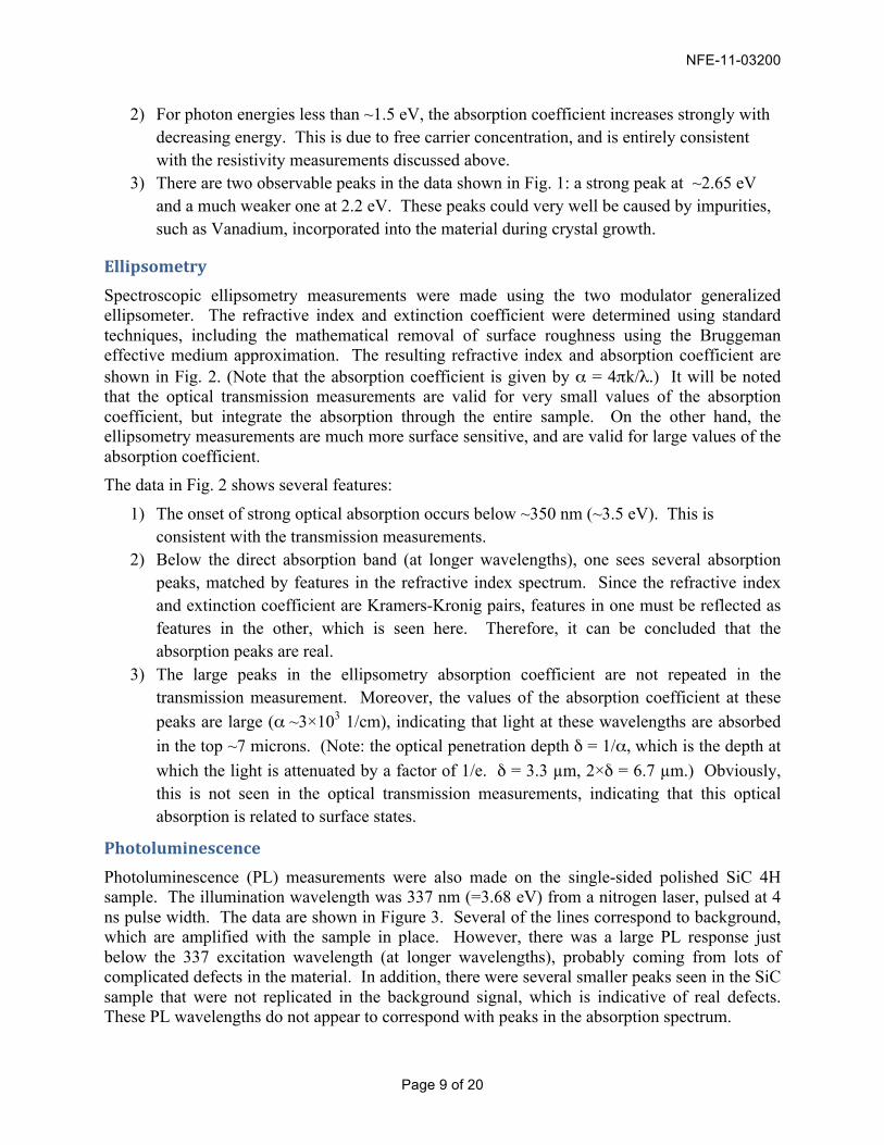
PTP processing provides similar process parameters to laser processing with the major difference being the pulse on time; consequently the same modeling approach can be used. Another discovery with PTP is its ability to generate high power wavelengths in the region less than 700 nm which provides overlap with the laser processing wavelengths of 532 nm and 355 nm which hold promise for simultaneously doping and activating dopants. In laser processing this may require two laser sources whereas PTP provides both simultaneously. SiC-‐4H: Material Properties The SiC material properties were evaluated in terms of optical, electrical, and photoluminescence characteristics. The results of our measurement and analysis are summarized in the following sections. Resistivity/Hall Effect Resistivity and Hall Effect measurements were taken in order to determine the type and extent doping present in the SiC material. Ohmic contacts were deposited at the 4 corners of the sample for I-V measurements. The resistivity of the sample was 20 milliohm-cm, but it was not possible to get good results from a Hall Effect measurement. Probable reason: The 1×1 cm2 sample was non-uniform. (This is expected for demonstration grade SiC). The low resistivity indicated that the carrier concentration was quite high, probably >1018 carriers/cm3. Since the Hall Effect measurements were inconclusive, it was not possible to ascertain the type, exact carrier concentration, or the mobility. The material conductivity modulations by PTP processing were evaluated in terms of surface resistance characteristics. Transmission Optical transmission measurements were taken on the double side polished SiC 4H sample, and then converted to the optical absorption coefficient, shown in Fig. 1. The data in figure 1 shows several features:
1) The onset of strong optical absorption occurs at ~3.5 eV ( ~350 nm). This is the fundamental band gap of the material.
NFE-11-03200
Page 9 of 20
2) For photon energies less than ~1.5 eV, the absorption coefficient increases strongly with decreasing energy. This is due to free carrier concentration, and is entirely consistent with the resistivity measurements discussed above.
3) There are two observable peaks in the data shown in Fig. 1: a strong peak at ~2.65 eV and a much weaker one at 2.2 eV. These peaks could very well be caused by impurities, such as Vanadium, incorporated into the material during crystal growth.
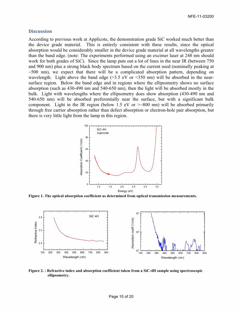
Ellipsometry Spectroscopic ellipsometry measurements were made using the two modulator generalized ellipsometer. The refractive index and extinction coefficient were determined using standard techniques, including the mathematical removal of surface roughness using the Bruggeman effective medium approximation. The resulting refractive index and absorption coefficient are shown in Fig. 2. (Note that the absorption coefficient is given by α = 4πk/λ.) It will be noted that the optical transmission measurements are valid for very small values of the absorption coefficient, but integrate the absorption through the entire sample. On the other hand, the ellipsometry measurements are much more surface sensitive, and are valid for large values of the absorption coefficient. The data in Fig. 2 shows several features:
1) The onset of strong optical absorption occurs below ~350 nm (~3.5 eV). This is consistent with the transmission measurements.
2) Below the direct absorption band (at longer wavelengths), one sees several absorption peaks, matched by features in the refractive index spectrum. Since the refractive index and extinction coefficient are Kramers-Kronig pairs, features in one must be reflected as features in the other, which is seen here. Therefore, it can be concluded that the absorption peaks are real.
3) The large peaks in the ellipsometry absorption coefficient are not repeated in the transmission measurement. Moreover, the values of the absorption coefficient at these peaks are large (α ~3×10³ 1/cm), indicating that light at these wavelengths are absorbed in the top ~7 microns. (Note: the optical penetration depth δ = 1/α, which is the depth at which the light is attenuated by a factor of 1/e. δ = 3.3 µm, 2×δ = 6.7 µm.) Obviously, this is not seen in the optical transmission measurements, indicating that this optical absorption is related to surface states.
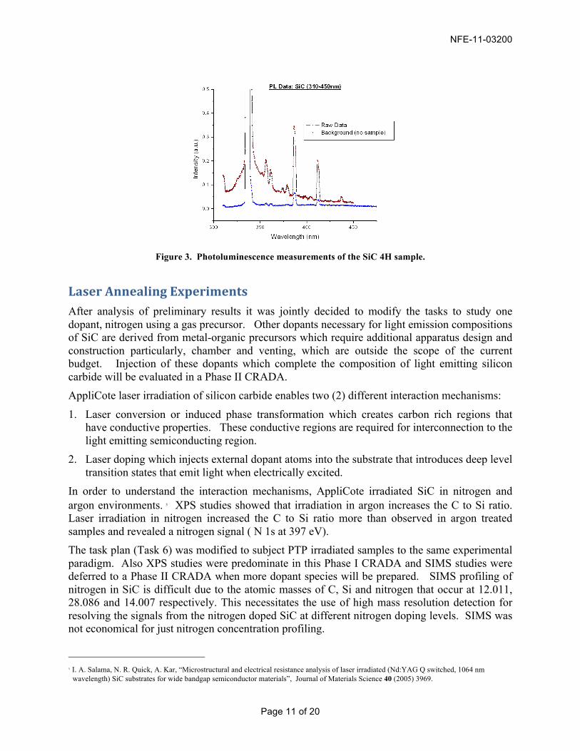
Photoluminescence Photoluminescence (PL) measurements were also made on the single-sided polished SiC 4H sample. The illumination wavelength was 337 nm (=3.68 eV) from a nitrogen laser, pulsed at 4 ns pulse width. The data are shown in Figure 3. Several of the lines correspond to background, which are amplified with the sample in place. However, there was a large PL response just below the 337 excitation wavelength (at longer wavelengths), probably coming from lots of complicated defects in the material. In addition, there were several smaller peaks seen in the SiC sample that were not replicated in the background signal, which is indicative of real defects. These PL wavelengths do not appear to correspond with peaks in the absorption spectrum.
NFE-11-03200
Page 10 of 20
Discussion According to previous work at Applicote, the demonstration grade SiC worked much better than the device grade material. This is entirely consistent with these results, since the optical absorption would be considerably smaller in the device grade material at all wavelengths greater than the band edge. (note: The experiments performed using an excimer laser at 248 nm should work for both grades of SiC). Since the lamp puts out a lot of lines in the near IR (between 750 and 900 nm) plus a strong black body spectrum based on the current used (nominally peaking at ~500 nm), we expect that there will be a complicated absorption pattern, depending on wavelength. Light above the band edge (>3.5 eV or <350 nm) will be absorbed in the near-surface region. Below the band edge and in regions where the ellipsometry shows no surface absorption (such as 430-490 nm and 540-650 nm), then the light will be absorbed mostly in the bulk. Light with wavelengths where the ellipsometry does show absorption (430-490 nm and 540-650 nm) will be absorbed preferentially near the surface, but with a significant bulk component. Light in the IR region (below 1.5 eV or >~800 nm) will be absorbed primarily through free carrier absorption rather than defect absorption or electron-hole pair absorption, but there is very little light from the lamp in this region.
Figure 1. The optical absorption coefficient as determined from optical transmission measurements.
Figure 2. : Refractive index and absorption coefficient taken from a SiC-4H sample using spectroscopic ellipsometry.
NFE-11-03200
Page 11 of 20
Figure 3. Photoluminescence measurements of the SiC 4H sample.
Laser Annealing Experiments After analysis of preliminary results it was jointly decided to modify the tasks to study one dopant, nitrogen using a gas precursor. Other dopants necessary for light emission compositions of SiC are derived from metal-organic precursors which require additional apparatus design and construction particularly, chamber and venting, which are outside the scope of the current budget. Injection of these dopants which complete the composition of light emitting silicon carbide will be evaluated in a Phase II CRADA. AppliCote laser irradiation of silicon carbide enables two (2) different interaction mechanisms:
1. Laser conversion or induced phase transformation which creates carbon rich regions that have conductive properties. These conductive regions are required for interconnection to the light emitting semiconducting region.
2. Laser doping which injects external dopant atoms into the substrate that introduces deep level transition states that emit light when electrically excited.
In order to understand the interaction mechanisms, AppliCote irradiated SiC in nitrogen and argon environments. 3 XPS studies showed that irradiation in argon increases the C to Si ratio. Laser irradiation in nitrogen increased the C to Si ratio more than observed in argon treated samples and revealed a nitrogen signal ( N 1s at 397 eV). The task plan (Task 6) was modified to subject PTP irradiated samples to the same experimental paradigm. Also XPS studies were predominate in this Phase I CRADA and SIMS studies were deferred to a Phase II CRADA when more dopant species will be prepared. SIMS profiling of nitrogen in SiC is difficult due to the atomic masses of C, Si and nitrogen that occur at 12.011, 28.086 and 14.007 respectively. This necessitates the use of high mass resolution detection for resolving the signals from the nitrogen doped SiC at different nitrogen doping levels. SIMS was not economical for just nitrogen concentration profiling.
3 I. A. Salama, N. R. Quick, A. Kar, “Microstructural and electrical resistance analysis of laser irradiated (Nd:YAG Q switched, 1064 nm
wavelength) SiC substrates for wide bandgap semiconductor materials”, Journal of Materials Science 40 (2005) 3969.
NFE-11-03200
Page 12 of 20
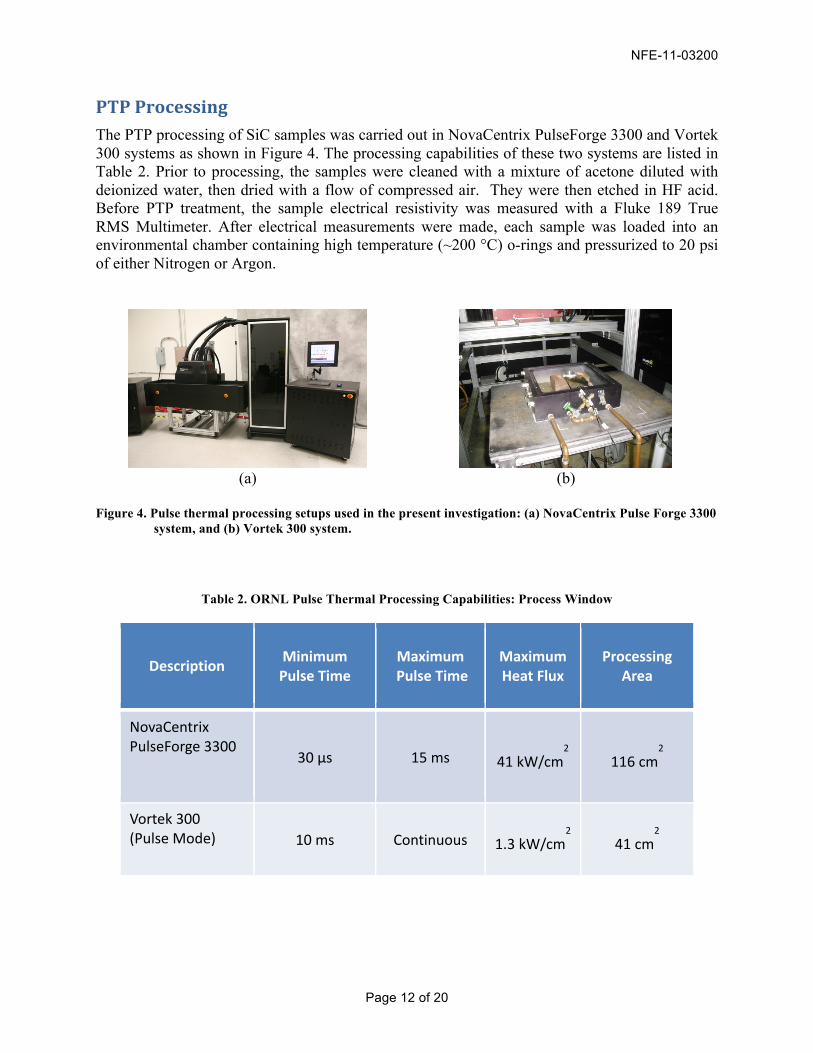
PTP Processing The PTP processing of SiC samples was carried out in NovaCentrix PulseForge 3300 and Vortek 300 systems as shown in Figure 4. The processing capabilities of these two systems are listed in Table 2. Prior to processing, the samples were cleaned with a mixture of acetone diluted with deionized water, then dried with a flow of compressed air. They were then etched in HF acid. Before PTP treatment, the sample electrical resistivity was measured with a Fluke 189 True RMS Multimeter. After electrical measurements were made, each sample was loaded into an environmental chamber containing high temperature (~200 °C) o-rings and pressurized to 20 psi of either Nitrogen or Argon.
(a) (b)
Figure 4. Pulse thermal processing setups used in the present investigation: (a) NovaCentrix Pulse Forge 3300
system, and (b) Vortek 300 system.
Table 2. ORNL Pulse Thermal Processing Capabilities: Process Window
Description Minimum Pulse Time
Maximum Pulse Time
Maximum Heat Flux
Processing Area
NovaCentrix PulseForge 3300
30 µs 15 ms 41 kW/cm2 116 cm
2
Vortek 300 (Pulse Mode) 10 ms Continuous 1.3 kW/cm
2 41 cm
2
NFE-11-03200
Page 13 of 20
Impact of PulseForge Annealing The PTP processing of the SiC samples in PulseForge 3300 system was carried out in the peak power range of 11-41 KW/cm2. The samples were enclosed in an environmental chamber under 20 psi N2 atmosphere. The investigated processing range did not show any influence on the surface morphology; as viewed under optical microscope, or electrical resistance of the samples. No thermal budget optimization was carried out at the first step as we wanted to analyze the influence of Vortek 300 processing on the material characteristics to make a better decision about the next step in dopant activation in SiC samples. Impact of Vortek 300 Processing Process Range
In Vortek 300 system; the sample was placed on the shuttle of the lamp for PTP processing, with metal guarding the environmental chamber hoses from lamp exposure. The lamp to sample offset distance was 2 cm. The samples were exposed to radiation with a peak power of 0.9 KW/cm2. The pulse duration and the number of pulses were varied in the ranges of 0.125-0.40s and 1-30; respectively. The investigated PTP process space mapped a total energy exposure range of 225-3600 J/cm2. Surface Morphology
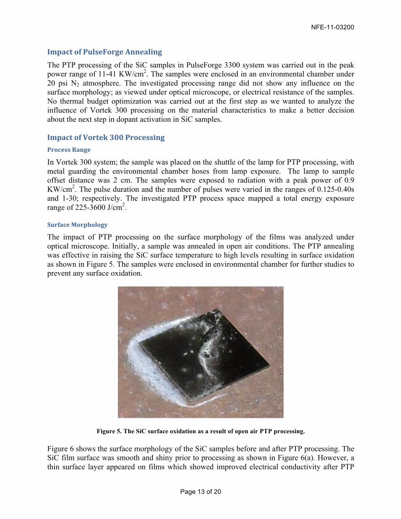
The impact of PTP processing on the surface morphology of the films was analyzed under optical microscope. Initially, a sample was annealed in open air conditions. The PTP annealing was effective in raising the SiC surface temperature to high levels resulting in surface oxidation as shown in Figure 5. The samples were enclosed in environmental chamber for further studies to prevent any surface oxidation.
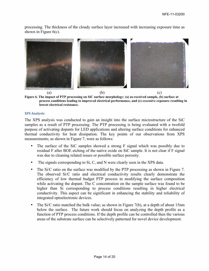
Figure 5. The SiC surface oxidation as a result of open air PTP processing. Figure 6 shows the surface morphology of the SiC samples before and after PTP processing. The SiC film surface was smooth and shiny prior to processing as shown in Figure 6(a). However, a thin surface layer appeared on films which showed improved electrical conductivity after PTP
NFE-11-03200
Page 14 of 20
processing. The thickness of the cloudy surface layer increased with increasing exposure time as shown in Figure 6(c).
(a) (b) (c)
Figure 6. The impact of PTP processing on SiC surface morphology: (a) as-received sample, (b) surface at process conditions leading to improved electrical performance, and (c) excessive exposure resulting in lowest electrical resistance.
XPS Analysis
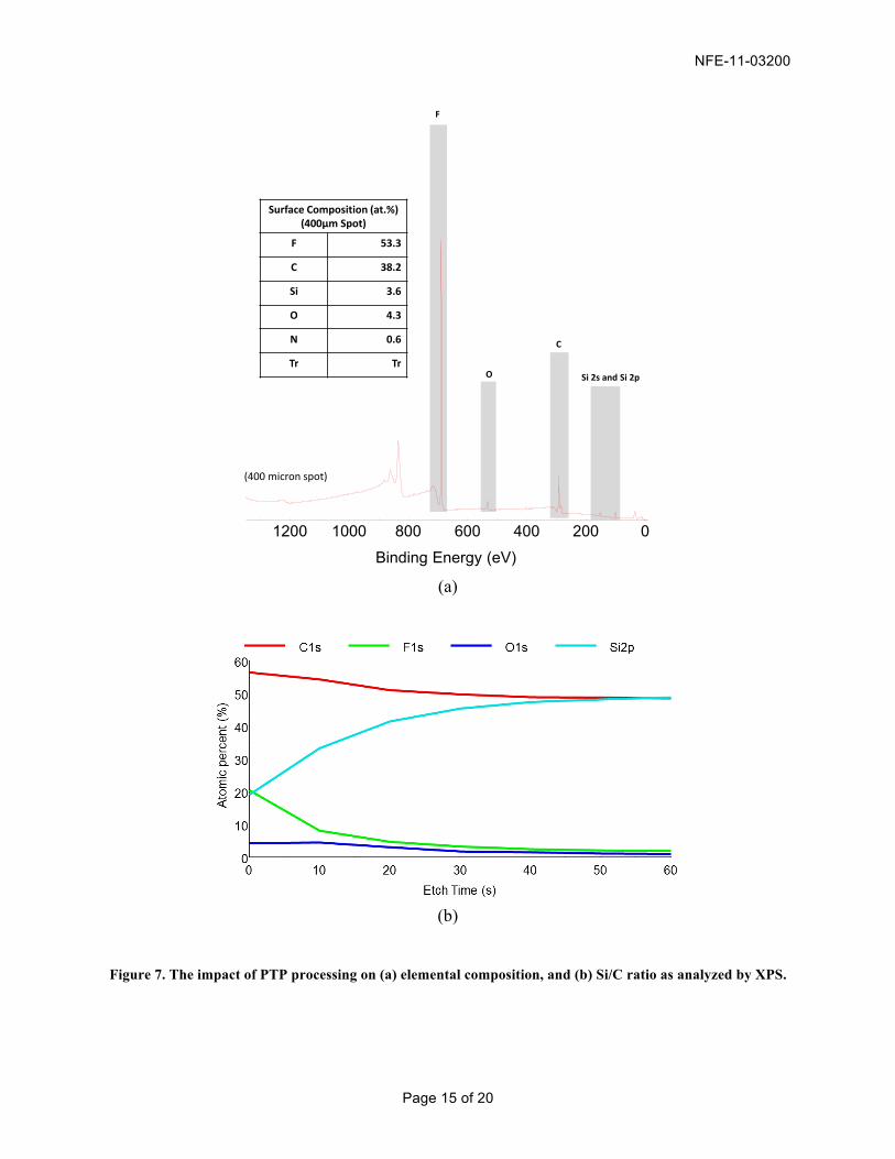
The XPS analysis was conducted to gain an insight into the surface microstructure of the SiC samples as a result of PTP processing. The PTP processing is being evaluated with a twofold purpose of activating dopants for LED applications and altering surface conditions for enhanced thermal conductivity for heat dissipation. The key points of our observations from XPS measurements; as shown in Figure 7, were as follows:
• The surface of the SiC samples showed a strong F signal which was possibly due to residual F after BOE etching of the native oxide on SiC sample. It is not clear if F signal was due to cleaning related issues or possible surface porosity.
• The signals corresponding to Si, C, and N were clearly seen in the XPS data.
• The Si/C ratio on the surface was modified by the PTP processing as shown in Figure 7. The observed Si/C ratio and electrical conductivity results clearly demonstrate the efficiency of low thermal budget PTP process in modifying the surface composition while activating the dopant. The C concentration on the sample surface was found to be higher than Si corresponding to process conditions resulting in higher electrical conductivity. This aspect can be significant in enhancing the stability and reliability of integrated optoelectronic devices.
• The Si/C ratio matched the bulk value; as shown in Figure 7(b), at a depth of about 15nm below the surface. The future work should focus on analyzing the depth profile as a function of PTP process conditions. If the depth profile can be controlled then the various areas of the substrate surface can be selectively patterned for novel device development.
NFE-11-03200
Page 15 of 20
(a)
(b)
Figure 7. The impact of PTP processing on (a) elemental composition, and (b) Si/C ratio as analyzed by XPS.
020040060080010001200
Binding Energy (eV)
(400 micron spot)
F
O
C
Si 2s and Si 2p
Surface Composition (at.%) (400µm Spot)
F 53.3
C 38.2
Si 3.6
O 4.3
N 0.6
Tr Tr
NFE-11-03200
Page 16 of 20
Electrical Performance
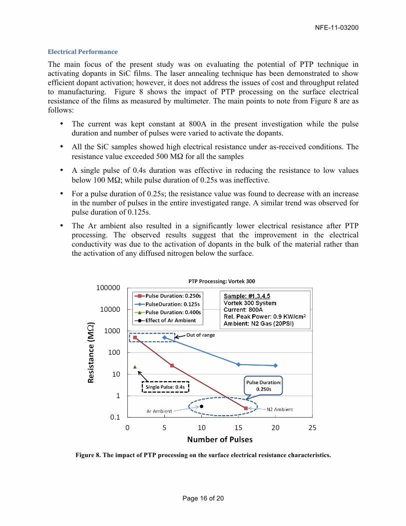
The main focus of the present study was on evaluating the potential of PTP technique in activating dopants in SiC films. The laser annealing technique has been demonstrated to show efficient dopant activation; however, it does not address the issues of cost and throughput related to manufacturing. Figure 8 shows the impact of PTP processing on the surface electrical resistance of the films as measured by multimeter. The main points to note from Figure 8 are as follows:
• The current was kept constant at 800A in the present investigation while the pulse duration and number of pulses were varied to activate the dopants.
• All the SiC samples showed high electrical resistance under as-received conditions. The resistance value exceeded 500 MΩ for all the samples
• A single pulse of 0.4s duration was effective in reducing the resistance to low values below 100 MΩ; while pulse duration of 0.25s was ineffective.
• For a pulse duration of 0.25s; the resistance value was found to decrease with an increase in the number of pulses in the entire investigated range. A similar trend was observed for pulse duration of 0.125s.
• The Ar ambient also resulted in a significantly lower electrical resistance after PTP processing. The observed results suggest that the improvement in the electrical conductivity was due to the activation of dopants in the bulk of the material rather than the activation of any diffused nitrogen below the surface.
Figure 8. The impact of PTP processing on the surface electrical resistance characteristics.
NFE-11-03200
Page 17 of 20
Summary and Direction This project has successfully demonstrated that a low thermal budget annealing technique, such as PTP, is critical to defining the path for low cost electronic devices integrated on glass or polymeric substrates. The observed results are attractive from manufacturing point of view as PTP technique offers significant advantages of large area processing, lower cost, and higher throughput as compared to laser annealing process. Additionally, PTP provides similar process parameters to laser processing while allowing sufficient pulse width for dopant activation. Another discovery with PTP is the ability to generate high intensity at wavelengths in the region below 700 nm, which overlaps with laser wavelengths of 532 nm and 355 nm, and thus shows the potential for simultaneously doping and activating dopants.
The main findings of our investigation; which are significant for the realization of SiC based optoelectronic devices, are as follows:
• The PTP technique is effective in low thermal budget activation of dopants in SiC similar to the laser technique. The surface electrical conductivity of the SiC samples improved by about three orders of magnitude as a result of PTP processing which is significant for charge injection in the devices.
• The surface composition of the SiC film can be modified by the PTP technique to create a carbon-rich surface (increased local C:Si ratio from 1:1 to 2.9:1). This is significant as higher thermal and electrical conductivities of the surface layer are critical for a successful development of integrated optoelectronic devices.
• PTP provides low thermal budget dopant activation with a controlled depth profile, which can be exploited for high performance device development with selective patterning of the substrate.
The following key focus areas have been identified for further exploration of the SiC based novel electronic device technology:
• Development of an LED device employing PTP dopant activation technique.
• Doping/Enhancing SiC conductivity by controlling environmental chamber atmosphere. o The present study was focused on nitrogen doped SiC samples. Other key dopants
necessary for light emission compositions of SiC are derived from metal-organic precursors which require additional apparatus design and construction particularly, chamber and venting, which were outside the scope of the current budget. Injection of these dopants which complete the composition of light emitting silicon carbide will be evaluated in a Phase II CRADA.
• Development of an LED device integrated on glass or other low temperature substrates.

NFE-11-03200
Page 18 of 20
Task Schedule
Task Number Task Description
Task Completion Date Progress Notes Original
Planned Revised Planned Actual Percent
Complete
1 Laser Thermal Modeling 12/31/10 6/1/11 8/1/11 100% Efforts at AppliCote supported by ORNL
2 Preliminary Laser
Processing 2/28/11 6/1/11 8/1/11 100% Efforts at AppliCote supported by ORNL
3 PTP Thermal Modeling 4/30/11 8/1/11 8/1/11 100% Completed optical analysis & modeling
4 Preliminary PTP
Processing 6/30/11 8/1/11 9/1/11 100% Completed on
Vortek and PulseForge tools
5 Modeling Light Emitting
Materials 8/31/11 8/1/11 100% Efforts at AppliCote supported by ORNL
6 Processing Light Emitting
Materials 10/31/11 9/30/11 9/30/11 100% Laser processing at
AppliCote, PTP at ORNL
7 Final Report 11/30/11 9/30/11 9/30/11 100% Complete

NFE-11-03200
Page 19 of 20
Spending Schedule Project Period: 11/31/10 to 09/30/11
Task Approved Budget
Project Expenditures
This Quarter Cumulative to Date
Task 1 Literature Review 28,000 $558 $11,657
Task 2 Prototype Design 50,000 $37,985 $58,184
Task 3 Prototype Fabrication 15,000 $7,404 $12,234
Task 4 Short-Term Testing 25,000 $16,116 $19,244
Task 5 Long-Term Testing 15,000 $3,116 $7,841
Task 6 Project Management 30,000 $37,232 $40,915
Task 7 Final Report 25,000 $15,751 $15,751
Materials & Travel 12,000 $8,742 $34,203
Total 200,000 $126,904 $200,031
DOE Share 100,000 $77,228 $100,000
Cost Share 100,000 $49,676 $100,031

NFE-11-03200
Page 20 of 20
Project Spending and Estimate of Future Spending
Calendar Year Quarter From To
Estimated Federal Share of Outlays*
Actual Federal Share of Outlays
Estimated Recipient Share of Outlays*
Actual Recipient Share of Outlays
Cumulative Actual Outlays
(Federal + Recipient)
1Q11 11/31/10 12/31/10 5,000 0 9,000 0 0
2Q11 1/1/11 3/31/11 25,000 $527 39,000 $23,758* $24,285
3Q11 4/1/11 6/30/11 40,000 $22,246 7,000 $26,597 $48,843
4Q11 7/31/11 9/30/11 5,000 $77,227 15,000 $49,676 $126,903
1Q12 10/1/11 11/31/11 25,000 n/a 30,000 n/a n/a
Totals 100,000 $100,000 100,000 $100,031 $200,031 * Reflects change in AppliCote’s accounting practice
Cost Share Contributions
Funding Source Approved Cost Share This Quarter Cumulative to Date
Cash In-Kind Cash In-Kind Cash In-Kind
AppliCote Associates 0 100 0 $49,676 0 $100,031
Total 0 100 0 $49,676 0 $100,031
Cumulative Cost Share Contributions $100,031