Embed Size (px)
Citation preview
NAZANIN KARIMI DIRECT LASER WRITING OF FLUORESCENT MICROSTRUCTURES CONTAINING SILVER NANOCLUSTERS IN POLYVINYL ALCOHOL FILMS Master of Science Thesis
Examiner: Dr. Juha Toivonen Examiner and topic approved by the Council of the Faculty of Natural Science on June 4, 2014
I
ABSTRACT
KARIMI, NAZANIN: Direct Laser Writing of Fluorescent Microstructures containing
Silver Nanoclusters in Polyvinyl Alcohol Films
Tampere University of Technology
Master of Science Thesis, 57 pages
April 2015
Master’s Degree Program in Science and Bioengineering
Major: Nanotechnology
Examiners: Dr. Juha Toivonen, M.Sc. Puskal Kunwar
Keywords: Metal nanoclusters, Polymer, Photopolymerization, Direct laser writing,
Spectroscopy, Photoluminescence, Photostability.
Metal nanoclusters (NCs), consisting of a few to few hundred atoms with dimensions
comparable to Fermi wavelength of electrons, exhibit significant molecular behavior. As a result
of quantum confinement effect, electrons which freely move in bulk metals become confined to
the spaces that can be as small as a few atom spacings. This confinement of electrons gives rise
to unique properties such as discrete energy levels, strong photoluminescence, and considerable
chemical reactivity. Therefore, synthesis of stable NCs could open the door to engineer novel
nanomaterials with tunable characteristics with a potential for numerous scientific and industrial
applications. However, NCs are not realized in practice as they are less stable than nanoparticles
(NPs). Hence, using proper stabilizer matrices is a requirement for synthesis of NCs. NCs can
be formed and stabilized in solutions by reducing dissolved metal ions in the presence of
organic molecules such as proteins, and polymers. Moreover, direct laser writing (DLW) is
shown to be a promising technique in fabrication and stabilization of metal NCs in polymer and
glass matrices.
In this thesis, we demonstrate the fabrication of highly fluorescent microstructures
containing silver NCs in polyvinyl alcohol (PVA) thin films using DLW technique. Polymer
thin films were prepared by spin-coating aqueous solutions of PVA containing silver nitrate on
glass substrates. Single-photon DLW were performed on silver-polymer films by tightly
focusing the continuous-wave (CW) laser beam of wavelength 405 nm, and scanning the sample
against the constant laser beam. Photoluminescence of the structures, dependence of the
fluorescence intensity on silver concentration and writing laser power, and photostability of the
fabricated microstructures were studied by using different optical characterization methods.
Atomic force microcopy (AFM) was used to estimate the thickness of the film, investigate the
surface topology, and measure the line width of the written structures.
The results showed broadband photostable fluorescence emissions from NCs at visible
wavelengths. Dependence of the fluorescence intensity on silver concentration confirmed that
the presence of silver in the polymer film is the cause of the bright luminescence. AFM analysis
of the written structures depicted the formation of grooves with depths of 35 ± 3 nm in a thin
film of 58 nm thickness. Moreover, it was observed that the breadth of the grooves, as well as
the emitted fluorescence intensity, increased with the writing power. The silver NCs fabricated
in this method were similar in character to NCs stabilized in organic solutions. Moreover, the
results were consistent with those obtained from the silver NCs fabricated in poly-methacrylic
acid (PMAA) films by using two-photon DLW technique. The outcomes of this work indicated
that single-photon DLW can be a useful method to sythesize highly fluorescent metal NCs with
any desired pattern in various kinds of polymer resins.
II
PREFACE
The Master of Science thesis ‘Direct Laser Writing of Fluorescent Microstructures
containing Silver Nanoclusters in Polyvinyl Alcohol Films’ was done in Optics
Laboratory of Department of Physics at Tampere University of Technology.
I would like to express my sincere gratitude to Dr. Juha Toivonen for providing me
the great opportunity of working on this interesting topic in Applied Optics group, and
for his guidance and supervision during the project. Special thanks to M.Sc. Puskal
Kunwar for patiently helping me to organize the experiments and sharing his helpful
knowledge and experience. I am also grateful to M.Sc. Jukka Hassinen from
Aalto University Nanomicroscopy Center for his help in AFM measurements, and the
Optoelectronic Research Center for letting me use their clean room facilities.
I would like to gratefully acknowledge Prof. Martti Kauranen, who gave me the
chance of working in the friendly environment of Optics Laboratory.
Finally, this thesis is dedicated to my parents whose limitless love and support have
always been the key to my success, and my dear Behnam for all his encouragement,
positive attitude, and affection.
Nazanin
Tampere, Finland
April 2015

III
CONTENTS
1. Introduction ............................................................................................................... 1 2. Nanoclusters .............................................................................................................. 4
2.1 Formation and growth of nanoclusters .............................................................. 5 2.2 Electronic structure of metal nanoclusters ........................................................ 8 2.3 Optical properties ............................................................................................ 13
2.4 Chemical reactivity ......................................................................................... 16 2.5 Stabilization of metal nanoclusters ................................................................. 18
3. Polymers .................................................................................................................. 21 3.1 Polyvinyl alcohol ............................................................................................ 22 3.2 Polymer processing ......................................................................................... 24
3.3 Effects of ambient conditions on polymeric materials .................................... 25
4. Photopolymerization ............................................................................................... 28
4.1 Polymerization processes ................................................................................ 28 4.2 Single-photon photopolymerization ................................................................ 30 4.3 Two-photon photopolymerization ................................................................... 32
5. Methodology ........................................................................................................... 35
5.1 Sample processing ........................................................................................... 35 5.2 Direct laser writing setup ................................................................................ 36
5.3 Fluorescence microscopy ................................................................................ 38 5.4 Fluorescence spectroscopy .............................................................................. 39 5.5 Atomic force microscopy ................................................................................ 41
6. Results ..................................................................................................................... 43 6.1 Polymer film analysis ...................................................................................... 43
6.2 Written structures ............................................................................................ 44
6.3 Effect of silver concentration .......................................................................... 45
6.4 Effect of laser writing power........................................................................... 46 6.5 Photobleaching of silver nanoclusters ............................................................. 47
7. Discussion and analysis .......................................................................................... 50
7.1 Material ablation ............................................................................................. 50 7.2 Enhanced Raman scattering effect .................................................................. 51
7.3 Bleaching parameters ...................................................................................... 53 8. Conclusion .............................................................................................................. 56 References ....................................................................................................................... 58
IV
LIST OF ABBREVIATIONS AND SYMBOLS
AFM Atomic Force Microcopy
BSA Bovine Serum Albumin
CV Cyclic Voltammetry
CW Continuous-wave
DFT Density Functional Theory
DLW Direct Laser Writing
DNA Deoxyribonucleic Acid
DP Degree of Polymerization
EA Electron Affinity
EDS Energy Dispersive x-ray Spectroscopy
EMCCD Electron Multiplying Charge Coupled Device
GC Glassy Carbon
HOMO Highest Occupied Molecular Orbital
IR Infrared
LED Light Emitting Diode
LUMO Lowest Unoccupied Molecular Orbital
MEMS Microelectromechanical Systems
MMD Molar Mass Distribution
NC Nanocluster
NIR Near-infrared
NP Nanoparticle
PAMAM Poly-amidoamine
PEI Polyethylenimine
PES Photoelectron Spectroscopy
PI Photo-initiator
PMMA Poly-methacrylic Acid
PPI Poly-propyleneimine
PVA Polyvinyl Alcohol
PVAc Polyvinyl Acetate
PVP Poly-vinylpyrrolidone
PS Photosensitizer
QD Quantum Dot
SEM Scanning Electron Microscopy
SPR Surface Plasmon Resonance
TPA Two-photon Absorption
UV Ultraviolet
vdW van der Waals
vis visible
1PP Single-photon Photopolymerization
2D Two-dimensional
2PP Two-photon Polymerization
3D Three-dimensional

V
A Affinity of phase transition
a Activity of particles in a solutiom
α Absorption coefficient
c Concentratiom
D Density of states
d Distance
ΔG Total free energy change
ΔGS Surface free energy change
ΔGV Volume free energy change
δ Absorption cross-section
E Energy
EF Fermi energy
Ekin Kinetic energy of electrons
εd Dielectric constant
Φ0 Polymer initiation
γ Surface energy per unit area
h Planck constant
ћ Reduced Planck constant
I Light intensity
J Rate of nucleation
k Wave number
kB Boltzmann constant
χ Electric susceptibility
λ Wavelength of light
M Monomer unit
Mn Macromolecule contains n monomers
MP Molecular weight of polymer
M0 Molecular weight of repeating units in a polymer
m Electron mass
μ Chemical potential
NA Avogadro number
ν, ω Light frequency
P Polarization
PI* Excited photo-initiator
PS* Excited photo-sensitizer
R Gass constant
R. Radical r Radius of a spherical cluster of atoms
r*
Radius above which the affinity of the transformation is positive
ρ Volume fraction occupied by nanoparticles
S Supersatiration parameter
S0 Ground electronic state
S1 Excited singlet state
T Temperature
Td,0 Initial polymer decomposition temperature
Td,1/2 The temperature of half decomposition of polymer
T1 Triplet state
tind Induction time
V Molecular volume
Ve Classical electrostatic potential

VI
Veff Effective potential
Vi External potential caused by ions
Vm Molar volume
Vxc Exchange potential
W The energy change per unit time, per unit volume
wt Weigth
1
1. INTRODUCTION
It has been a long time since the significance of nanotechnology was remarked by
Feynman in 1959 when he presented his famous lecture entitled “there is plenty of room
at the bottom”. Developing new techniques for synthesis of nanomaterials, as well as
advanced tools for their manipulation and characterization, has fueled the development
of nanoscience and technology during last years. [1] The major demand of this field has
been shrinking the dimensions of materials in order to make an advantage from the
unique properties they exhibit in nanometer scale. According to their characteristic
length scales, nanomaterials are classified to nanoparticles (NPs) with diameters larger
than 2 nm, and nanoclusters (NCs) with the size smaller than 2 nm (comparable with the
Fermi wavelength of electrons). [2] The ability to synthesize and characterize such
ultra-small clusters, has opened the door to a new field which builds a bridge between
atomic and NP behavior. Also, it leads to the contribution of different disciplines of
physics, chemistry, materials science, biology, medicine, and environmental sciences.
[3]
The main focus of this thesis work is on metal NCs, which have been studied by
researchers from a long time ago. Due to quantum confinement effect, metal NCs
exhibit novel optical, electrical, and catalytic properties significantly different from not
only their bulk counterparts, but also larger NPs. One of the remarkable features of such
molecule-like metal NCs is their significant photoluminescence, which has made them
attractive materials for lots of studies. More specifically, synthesis and characterization
of water-soluble noble metal NCs (e.g., gold and silver) have attracted lots of attention
since 1990s. Their intense fluorescence, low toxicity, and ultra-fine size have proposed
them as interesting materials for applications in optical data storage, sensing,
bioimaging, and biolabeling. [2, 4] Great interest in taking advantage of metal NCs
properties have motivated researchers to work intensively on developing the methods of
NCs synthesis. The main difficulty of synthesizing metal NCs is their strong tendency
to aggregate and form larger particles, which no longer exhibit the significant properties
such as strong luminescence [5]. Therefore, great effort has been made to find feasible
and affordable techniques for growing NCs and stabilizing them in order to prevent
their agglomeration. Successful synthesis of fluorescent metal NCs in various organic
and inorganic stabilizing matrices such as polymers [5], dendrimers [6],
deoxyribonucleic acid (DNA) [7], glasses [8], and zeolites [9] have been reported. In
this thesis work, steric stabilization approach by utilizing polymer agents is used to
synthesize silver NCs. Polymers have been shown to be excellent matrices to grow
strongly fluorescent metal NCs. Aqueous solutions of a variety of polymers such as
2
polyphosphate, polyacrylate, poly-methacrylic acid (PMMA), and polyvinyl alcohol
(PVA), which are known for stabilization of colloidal particles, can be appropriate for
this purpose [5, 10, 11]. The mostly used process for polymer stabilization of NCs
includes reduction of metal ions to zero-valent atoms within the polymer solution,
followed by coalescence of polymer molecules surrounding the NCs through
polymerization process. This thesis is concerned with photo-induced polymerization
process, which has become a well-known and beneficial method of polymerization, as a
consequence of developments in laser technology. Single-photon absorption by using
conventional high-frequency laser sources, and multi-photon absorption by utilizing
near-infrared (NIR) femtosecond (fs) lasers are two primary mechanisms of
photopolymerization. By employing the technique of direct laser writing (DLW), either
of these two mechanisms can be applied to selectively polymerize the polymer films
and fabricate patterned structures containing fluorescent metal NCs.
DLW has been a very beneficial tool to modify, add, and subtract materials from
nanometer to millimeter scales for a variety of applications in photolithography,
microelectronics, nanophotonics, biomedicine, etc. In general, DLW refers to a
technique used to create two-dimensional (2D) or three-dimensional (3D) structures
without any need of masks or pre-existing templates. Moreover, development of laser
technology has reinforced DLW as a fast and cost-effective way to produce novel
structures and devices. [12] Fabrication of silver NC in inorganic matrices through
DLW was reported several years ago by Bellec et al. [8] and De Cremer et al. [9].
Recently, Kunwar et al. have published the first employment of DLW in an
organic matrix [5]. They fabricated 2D fluorescent structures containing silver NCs in
PMMA thin films through the two-photon absorption process. In general, fabrication of
3D structures is more feasible by using two-photon absorption approach while
2D structures can be constructed by applying either of two processes. Therefore, the
concern of this thesis is fabricating such photostable fluorescent microstructures in
organic matrices by using single-photon absorption mechanism. The organic matrix we
use for this purpose is PVA, a water-soluble polymer with excellent film-forming and
stabilizing properties. Thin films of PVA containing metal particles can be readily
prepared on glass substrates through simple methods such as spin-coating. Afterward,
DLW on polymer films can be done by collimating and tightly focusing the light beam
into the resin. Typically, patterning is attained by either scanning the laser beam over a
fixed surface or moving the sample within the fixed beam [12].
This thesis consists of eight chapters including the introduction. Chapter 2 provides
information about NCs, specifically metal NCs, principles of cluster formation and
growth, important electronic, optical and chemical properties of NCs, and the methods
of cluster stabilization. General aspects of polymers with a focus on PVA properties,
introducing spin-coating as a method of polymer processing, and conditions leading to
degradation of polymers are included in Chapter 3. After presenting some fundamental
information about polymers, the process of polymerization with a particular attention to
photo-induced polymerization and its primary mechanisms (single-photon and

3
two-photon polymerizations) are discussed in Chapter 4. The theoretical background of
the thesis is followed by Chapter 5, which provides information about experimental
methods and setups used for the sample preparation, DLW of silver NCs, and their
characterization. The results of the experiments are presented in Chapter 6, and some of
them are further discussed in Chapter 7. Finally, Chapter 8 concludes this thesis work,
and it is followed by the list of references used for this project.
4
2. NANOCLUSTERS
In physics and chemistry the term “Nanocluster (NC)” refers to a group of few to few
hundreds atoms of the same element, usually a metal, bonded closely together [3]. The
dimension of NCs is typically less than 2 nm comparable with Fermi wavelength of
electrons. In this dimension, metal NCs exhibit typical molecular behavior leading to
privileged electronic, optical and chemical properties. [11]
The properties of metals significantly change when they scale down from bulk to
small NCs. Freely moving electrons in the conduction band of bulk metals are
responsible for their electrical conductivity and optical reflectance. As the dimensions
of metal shrink down to the size of NPs, the metallic features disappears. Instead,
a surface plasmon resonance (SPR) effect, which is the characterization of metal NPs,
causes intense colors when particles interact with light. When the size of metal is further
reduced to less than 2 nm, the plasmonic properties also disappear. The
continuous density of states in bulk metals breaks down into discrete energy levels. As a
result of electronic transitions between discrete levels, NCs exhibit features such
as significant light absorption and emission. In fact, metal NCs act as a bridge between
metal atoms and NPs. [11, 13]
Significant properties of metal NCs such as ultra-small size and strong fluorescence
make them attractive materials for applications in single-molecule studies, fluorescence
imaging, fluorescence sensing, optical data storage, and labeling. Particularly, silver
NCs which are synthesized in organic matrices have a great potential to be used as
fluorescent biolabels due to their biocompatibility, intense brightness, and
photostability. Moreover, as the optical response of the NCs depends on their interaction
with organic scaffolds, they can be utilized as sensitive probes. [13]
NCs can be synthesized in solutions by reducing metal ions from dissolved metal
salt using chemical reductants, light, or γ-rays. However, the growth of the NCs needs
to be stabilized since they have a large tendency to aggregate and decrease their surface
energy. Therefore, utilizing a stabilizer agent to prevent NCs agglomeration is essential
in order to use their significant properties for real applications.
In this chapter, the physical principles of formation and growth of NCs are briefly
explained. Afterward, the electronic structure of metal NCs is studied that is followed
by introducing their important optical and chemical properties. Finally, different
approaches for stabilization of metal NCs are introduced.
5
2.1 Formation and growth of nanoclusters
Understanding the details of NCs growth process is beneficial to control their desired
properties. NCs can be synthesized using various methods such as chemical reduction,
photoreduction, thermal decomposition, ligand reduction and displacement from
organometallics, metal vapor synthesis, and electrochemical synthesis [14]. Chemical
reduction and photoreduction of metal ions in suitable encapsulating media such as
dendrimers, polymers, DNA, etc. are the most common methods of NC synthesis [13].
Preparation of wet chemical NCs and NPs using chemical reduction have been used for
several decades [15]. For the first time, this reduction method was applied by Faraday in
1857 during his studies on gold sols [16]. That includes the reduction of metal ions to a
zero-valent state in an aqueous or organic media and stabilizing them to avoid further
growth of particles [5, 15]. In addition to chemical reduction, photoreduction methods
have been proved to be very useful to synthesize noble metal NCs. Activation with light
enables control of the reduction process without introducing undesired impurities, and
the interaction can be initiated homogenously. [17]
After reduction of metal ions, the nucleation of atoms occurs that is followed by the
growth of clusters by adding colloidal particles to the formed seed nucleus [15]. In order
to understand the growth of NCs, one needs to comprehend the classical
nucleation process which is the perquisite for studying NCs and NPs growth [18].
Classical theory of nucleation describes the condensation of vapor molecules to primary
spherical liquid droplets. This theory has been expanded to crystallization from
solutions as well. [19] Nucleation can be either spontaneous (homogeneous nucleation)
or induced (heterogeneous nucleation). Homogeneous nucleation happens in the
absence of any impurity species while heterogeneous nucleation occurs when nucleation
is affected by the presence of impurities. [20] In primary homogeneous nucleation,
solute atoms or molecules in a supersaturated solution combine to generate clusters as
the growth of a nucleus reduces the Gibbs free energy of the system [19, 21].
Nucleation initiates as a result of thermodynamic imbalance between the liquid phase
and solid phase leading to the phase transition. Affinity of the transition A is a
thermodynamic force that causes the phase shift. It is the result of the difference
between chemical potentials μ of the two phases:
𝐴 = 𝜇1 − 𝜇2 . (1)
Chemical potential is defined by
𝜇 = 𝜇0 + 𝑅𝑇 ln 𝑎 . (2)
Here, 𝜇0 is the standard potential, 𝑅 is the gas constant, 𝑇 is the temperature and 𝑎 is
the activity of particles in the solution. Chemical potential of a spherical cluster with
radius 𝑟 is
6
𝜇(𝑟) = 𝜇2 + (2𝛾 𝑟⁄ )𝑉𝑚 , (3)
where 𝜇2 is the chemical potential of the bulk material, 𝛾 is the interfacial tension or
surface energy per unit area, and 𝑉𝑚 is the molar volume. Thus, the affinity of the phase
transformation is
𝐴 = 𝜇1 − (𝜇2 + (2𝛾 𝑟⁄ )𝑉𝑚) . (4)
The value of the thermodynamic force 𝐴 has to be positive in order to convert liquid
phase to the solid phase. That means that the phase change happens only when particles
are adequately large. For a certain ∆𝜇 = |𝜇1 − 𝜇2|, the critical radius 𝑟∗ is defined as a
radius above which the affinity of the transformation is positive and the NC will grow
[18, 20]
𝑟∗ = (2𝛾 ∆⁄ 𝜇)𝑉𝑚 . (5)
∆𝜇 defines the difference between values of free energy per mole for bulk states of
two phases. If the cluster grows into a sphere with radius 𝑟, the total free energy change
∆𝐺 is sum of the change in surface free energy ∆𝐺𝑆 and change in free energy of the
cluster volume ∆𝐺𝑉
∆𝐺 = ∆𝐺𝑆 + ∆𝐺𝑉 = 4𝜋𝑟2𝛾 − (4𝜋𝑟3 3𝑉𝑚 )⁄ ∆𝜇 . (6)
Then, the free energy change for the cluster with critical radius is defined by
∆𝐺∗ = (16𝜋 3)(𝛾3𝑉𝑚 2 ∆𝜇2) .⁄⁄ (7)
The rate of nucleation, which is the number of particles nucleated per cubic centimeter
per second, is described by Arrhenius equation:
𝐽 = 𝐴 exp(−∆𝐺∗ 𝑘𝐵𝑇⁄ )
= 𝐴 exp[−(16𝜋 3⁄ )(𝛾3𝑉𝑚 2 ∆𝜇2𝑘𝐵𝑇⁄ )] ,
(8)
where 𝑘𝐵 is the Boltzmann constant. Considering the equation (2), by using a valid
approximation, the chemical potential difference can be defined as a function of
supersaturation parameter 𝑆
∆𝜇 = 𝑅𝑇 ln 𝑆 , (9)
where 𝑆 = 𝑐 𝑐0⁄ is a ratio of the solute concentration 𝑐 to the saturation concentration
𝑐0. Then the nucleation rate as a function of supersaturation degree is
7
𝐽 = 𝐴. exp[−(16𝜋 3⁄ )(𝛾3𝑉 2 𝑘𝐵
3𝑇3ln 𝑆2⁄ )] , (10)
𝑉 = 𝑉𝑚 𝑁𝑎⁄ is the molecular volume where 𝑁𝑎 is the Avogadro number. [20] Applying
the equation (9) in equations (5) and (7), one can conclude for 𝑆 > 1, increasing 𝑆
results in decreasing the critical size and consequently the energy barrier. Thus, the
probability of growing sufficiently large clusters which can overcome the barrier and
become stable will be enhanced. That means a higher rate of nucleation, which is
evident from equation (10). [18] This equation is the standard expression for primary
homogeneous nucleation rate which shows three major variables: the temperature, the
supersaturation degree, and the interfacial tension [18, 20]. The most cited example of
applying the nucleation theory to cluster formation is the work of LaMer in 1950s on
the formation of sulfur sols [22]. Turkevitch was the first one who proposed the
stepwise formation and growth of gold NCs based on nucleation soon after LaMer in
1951 [23]. Later, thermodynamic and kinetic studies with the help of modern analytical
techniques have considerably modified the model, and several reviews have been
published including those complementary theories. Nowadays, development of
computational chemistry has made it possible to design sophisticated NCs exhibiting
desired behaviors for specific applications. [15]
Different experimental methods were also used to measure the kinetics of cluster
formation during last decades. In 1960s Nielson performed some experimental
measurements and proposed an empirical description of the primary nucleation process
using an induction time 𝑡𝑖𝑛𝑑
𝑡𝑖𝑛𝑑 = 𝑘 × 𝑐1−𝜌 , (11)
where 𝑘 is a constant, 𝑐 is the concentration of the supersaturated solution, and 𝜌 is the
number of particles required to create the critical nucleus [24]. Since then,
several spectroscopic techniques have been developed to measure kinetics of NCs
formation and their dimensions. Dynamic light scattering to acquire information about
clusters size in solutions, ultraviolet (UV)-visible spectroscopy, and x-ray spectroscopy
to study the kinetics of cluster formation are examples of those methods. However,
there is no precise quantitative experimental description of metal NCs formation
kinetics in solutions. Most of the experimental methods are able to measure kinetics of
larger clusters not the nucleation process. [25]
Nucleation and growth of the clusters have been profoundly studied theoretically.
Although the classical nucleation theory is a logical starting point to investigate the
formation of metal NCs, it is a simplified explanation of a complicated process. This
theory treats the nucleus as a bulk material and assumes that the surface free energy of
the cluster is the same as that for an infinite planar surface. Both of these assumptions
need to be modified when studying small clusters including few atoms. [25] Moreover,
the energy of cluster formation determined based on this theory, does not include any
information about the structure of the cluster. Early stage mass spectroscopy
8
experiments have resulted in prominently high concentration of clusters with specific
numbers of atoms called magic numbers. [19] These particles composed of sequentially
packing layers of atoms around a single atom and possess hexagonal or cubic close
packing structures which built stepwise by nucleation of specific numbers of atoms
(magic numbers). The allowed number of particles which can be added to a full-shell
cluster including n shell to construct the (n+1) shell is determined by 10n2+2. This
formula suggests 13, 55, 147, 309 atoms and so on for the size of clusters. [14, 15] Most
of the nanoclusters possess geometries close to that of magic clusters. Since the
maximum number of metal-metal bonds is formed in full-shell geometries, they are
more stable. [14] However, classical theory is not able to predict this phenomenon [19].
Furthermore, the systems in classical theory are considered to be in equilibrium and
nucleation occurs slowly. Fast nucleation systems with extreme collapse cannot
be studied only using the classical theory. Moreover, the nucleation rate in the theory is
defined by addition of one single atom to the sub-critical nucleus. In the case of multi
atoms addition like cluster-cluster collisions, reconsidering the formulation is essential.
Thus, to overcome these weaknesses and provide a comprehensive formulation,
complementary methods determine the binding energies of clusters with various
geometries through ab initio quantum mechanical calculations. The concentration
development of different sized clusters with time can be also predicted based on a
population balance theory of nucleation considering all possible collisions of clusters
and associated energies. Thus, the required time to grow the highest concentration of a
cluster with a particular size is predictable. It allows tuning experimental conditions in
order to maximize the concentration of a cluster possessing a desired size. [19] This
ability of size tuning is significant since the electronic structure, optical absorption, and
catalytic properties of NCs are strongly influenced by their dimensions. Some of these
size dependent features will be discussed in the following.
2.2 Electronic structure of metal nanoclusters
Continuous shrinking the size of bulk metals to NCs causes significant changes in their
properties since the bulk behaviors are due to an infinite number of their building blocks
[26]. Electronic structure of nanoscale particles with dimensions more than 1 nm
depends on the number of atoms they include, and is intermediate between the
electronic structure of molecules and that of the bulk materials. Ultra-small NCs with a
size less than 1nm, exhibit a typical molecular behavior while there are still some
structural relations to their bulk counterparts [27, 26]. Therefore, in contrast to bulk
metals that behave based on classical laws, NCs containing few atoms follow quantum
mechanical rules; and, their properties strongly depend on the exact number of their
atoms. [27]
In bulk materials, orbitals with similar energy states combine and make electronic
energy bands. In the case of semiconductor and insulating crystals, there is always an
energy gap between the valence and conduction bands, and bonding varies from weak
9
van der Waals (vdW) to strong covalent or ionic bonds. In bulk metals, the band gap
disappears at Fermi level, and metallic bonding arises from delocalization of electrons.
The valence band is completely occupied by valence electrons and the conduction band
as a result of overlap with the valence band is partially filled with electrons, which are
responsible for conductivity of metals. By ceaselessly decreasing the size of metal
particles to nanoscale dimensions, the overlap of valence and conduction bands weakens
and a band gap similar to that in semiconductors appears. [3] Therefore, small NPs
always exhibit an energy gap between the highest occupied molecular orbital (HOMO)
and lowest unoccupied molecular orbital (LUMO) either they consist of metallic or
nonmetallic elements. Consequently, nanoscale metals do not contribute in metallic
bondings as their corresponding crystals do. Further miniaturize the size of the metal
particles, results in formation of the NCs with more or less discrete energy levels. [3,
27] At this point, the size of a metal NC is comparable to the De Broglie wavelength of
electrons with energy comparable to Fermi energy (EF) of metals. Thus, the NC behaves
analogous to a quantum dot (QD) for electrons. [28] As a result of quantum size effect,
the free carrier is now quantum confined and behaves according to quantum mechanical
‘particle in a box’ model. The solutions of the Schrödinger equation for such a system
are bounded standing waves in a potential well, which associate with quantized
and discrete energy levels. [29] The structure of energy levels in this dimension will
change by altering the size of the NC [28]. Further shrinking the size of the NC to less
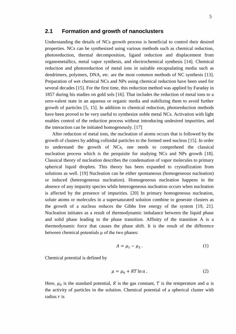
than 1 nm yields to a typical molecular situation [27]. Figure 1 illustrates the electronic
structure development from overlapping energy bands in bulk metal to discrete levels in
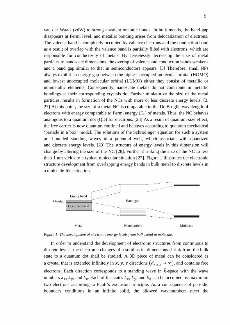
a molecule-like situation.
Figure 1: The development of electronic energy levels from bulk metal to molecule.
In order to understand the development of electronic structures from continuous to
discrete levels, the electronic changes of a solid as its dimensions shrink from the bulk
state to a quantum dot shall be studied. A 3D piece of metal can be considered as
a crystal that is extended infinitely in 𝑥, 𝑦, 𝑧 directions (𝑑𝑥,𝑦,𝑧 → ∞), and contains free
electrons. Each direction corresponds to a standing wave in -space with the wave
numbers 𝑘𝑥, 𝑘𝑦, and 𝑘𝑧. Each of the states 𝑘𝑥, 𝑘𝑦, and 𝑘𝑧 can be occupied by maximum
two electrons according to Pauli’s exclusion principle. As a consequence of periodic
boundary conditions in an infinite solid, the allowed wavenumbers meet the
Band gap
Occupied band Overlap
Empty band
Metal Nanoparticle Molecule
10
condition 𝑘𝑥,𝑦,𝑧 = ±𝑛𝑥,𝑦,𝑧∆𝑘 = ±𝑛𝑥,𝑦,𝑧2𝜋𝑑𝑥,𝑦,𝑧⁄ , where 𝑛 is an integer number. Since
𝑑𝑥,𝑦,𝑧 in a bulk solid is large, ∆𝑘 tends toward zero. The energy of free electrons is
proportional to the square value of the wavenumber, 𝐸(𝑘𝑥,𝑦,𝑧) = (ћ22𝑚⁄ )𝑘𝑥,𝑦,𝑧
2,
where ћ is the reduced Planck constant, and 𝑚 is the electron mass. That leads to
quasi-continuous energy states and the density of states 𝐷3𝑑(𝐸), which varies with
square-root of the energy (𝐷3𝑑(𝐸) ∝ 𝐸12⁄ ). If the size of metal in any of three infinite
directions decreases to a few nanometers, the electrons cannot move freely anymore,
and they will be confined in that particular direction resulting to quantized energy states.
Reducing the size of one dimension to few nanometers leads to a system called
two-dimensional electron gas or quantum well. For instance, in a 2D solid extended
infinitely along 𝑥 and 𝑦 directions, 𝑘𝑧 is allowed to contain only discrete values. The
smaller 𝑑𝑧, the larger ∆𝑘𝑧 between quantized states. The energy states diagram is still
quasi-continuous while the density of states corresponds to a step function. Therefore,
the original electrons of the metal which were able to move freely in three dimensions
now are allowed to move in only two dimensions. Diminishing the size of the solid
along the second direction, for example, 𝑦 dimension yields the confinement of
electrons in two directions. The system is called one-dimensional electron system or
quantum wire. The values of ∆𝑘 in 𝑦 and 𝑧 directions are quantized, but it is not the
case along 𝑥 direction. Therefore, the energy diagram is a parabola with ∆𝑘𝑥 → 0. The
density of states depends on 𝐸−12⁄ and for each discrete 𝑘𝑦 and 𝑘𝑧 state result in a
hyperbolic curve that exhibits continuous distribution of 𝑘𝑥 states. The next step is to
shrink the size of 𝑥 direction as well in order to include a zero-dimensional quantum dot
system. Now, the electrons are confined in all three dimensions and only discrete values
for 𝑘𝑥,𝑦,𝑧 are acceptable. Therefore, the energy levels are completely quantized, and the
density of states contains delta peaks. In a QD system, the last few metallic electrons are
enclosed in three dimensions and because of quantum size effects they behave such as
particles in a box. These electrons are responsible for significant change of physical and
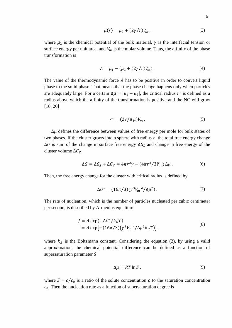
chemical characteristics of metal clusters. [26, 27, 29] Figure 2 indicates the evolution
of density of states as a function of the electrons energy from a bulk metal to a
nanocluster.
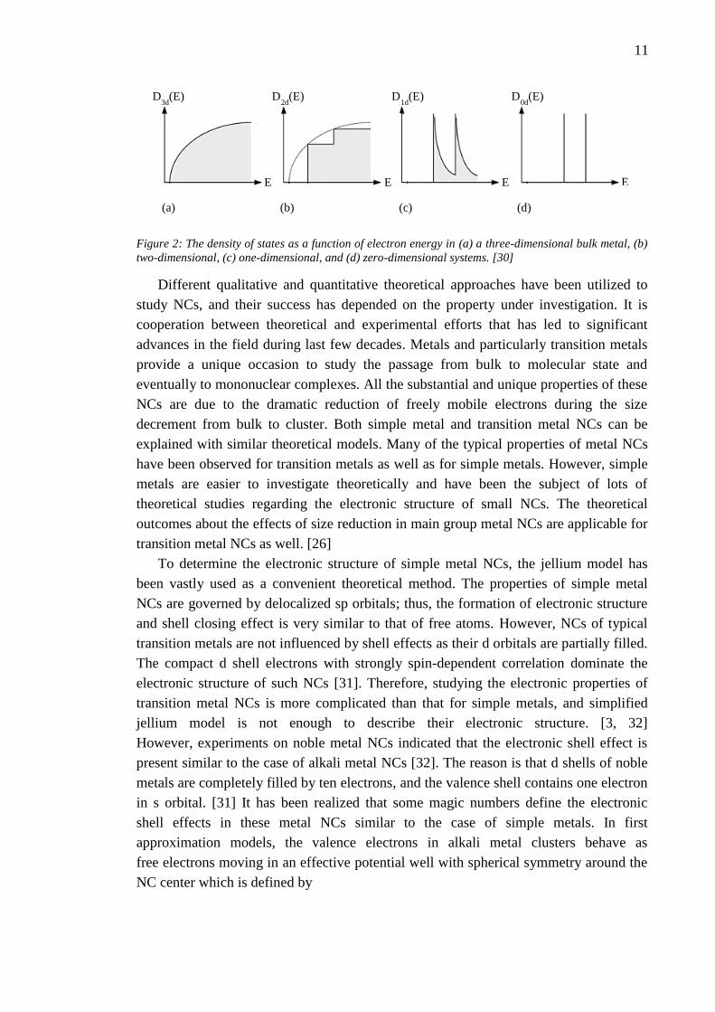
11
Figure 2: The density of states as a function of electron energy in (a) a three-dimensional bulk metal, (b)
two-dimensional, (c) one-dimensional, and (d) zero-dimensional systems. [30]
Different qualitative and quantitative theoretical approaches have been utilized to
study NCs, and their success has depended on the property under investigation. It is
cooperation between theoretical and experimental efforts that has led to significant
advances in the field during last few decades. Metals and particularly transition metals
provide a unique occasion to study the passage from bulk to molecular state and
eventually to mononuclear complexes. All the substantial and unique properties of these
NCs are due to the dramatic reduction of freely mobile electrons during the size
decrement from bulk to cluster. Both simple metal and transition metal NCs can be
explained with similar theoretical models. Many of the typical properties of metal NCs
have been observed for transition metals as well as for simple metals. However, simple
metals are easier to investigate theoretically and have been the subject of lots of
theoretical studies regarding the electronic structure of small NCs. The theoretical
outcomes about the effects of size reduction in main group metal NCs are applicable for
transition metal NCs as well. [26]
To determine the electronic structure of simple metal NCs, the jellium model has
been vastly used as a convenient theoretical method. The properties of simple metal
NCs are governed by delocalized sp orbitals; thus, the formation of electronic structure
and shell closing effect is very similar to that of free atoms. However, NCs of typical
transition metals are not influenced by shell effects as their d orbitals are partially filled.
The compact d shell electrons with strongly spin-dependent correlation dominate the
electronic structure of such NCs [31]. Therefore, studying the electronic properties of
transition metal NCs is more complicated than that for simple metals, and simplified
jellium model is not enough to describe their electronic structure. [3, 32]
However, experiments on noble metal NCs indicated that the electronic shell effect is
present similar to the case of alkali metal NCs [32]. The reason is that d shells of noble
metals are completely filled by ten electrons, and the valence shell contains one electron
in s orbital. [31] It has been realized that some magic numbers define the electronic
shell effects in these metal NCs similar to the case of simple metals. In first
approximation models, the valence electrons in alkali metal clusters behave as
free electrons moving in an effective potential well with spherical symmetry around the
NC center which is defined by
D3d
(E) D2d
(E) D1d
(E) D0d
(E)
(a) (b) (c) (d)
E E E E
12
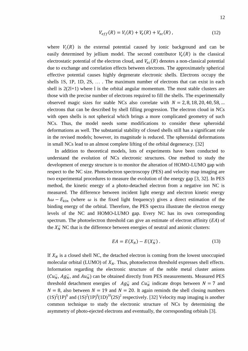
𝑉𝑒𝑓𝑓(𝑅) = 𝑉𝑖(𝑅) + 𝑉𝑒(𝑅) + 𝑉𝑥𝑐(𝑅) , (12)
where 𝑉𝑖(𝑅) is the external potential caused by ionic background and can be
easily determined by jellium model. The second contributor 𝑉𝑒(𝑅) is the classical
electrostatic potential of the electron cloud, and 𝑉𝑥𝑐(𝑅) denotes a non-classical potential
due to exchange and correlation effects between electrons. The approximately spherical
effective potential causes highly degenerate electronic shells. Electrons occupy the
shells 1S, 1P, 1D, 2S, … . The maximum number of electrons that can exist in each
shell is 2(2l+1) where l is the orbital angular momentum. The most stable clusters are
those with the precise number of electrons required to fill the shells. The experimentally
observed magic sizes for stable NCs also correlate with 𝑁 = 2, 8, 18, 20, 40, 58, …
electrons that can be described by shell filling progression. The electron cloud in NCs
with open shells is not spherical which brings a more complicated geometry of such
NCs. Thus, the model needs some modifications to consider these spheroidal
deformations as well. The substantial stability of closed shells still has a significant role
in the revised models; however, its magnitude is reduced. The spheroidal deformations
in small NCs lead to an almost complete lifting of the orbital degeneracy. [32]
In addition to theoretical models, lots of experiments have been conducted to
understand the evolution of NCs electronic structures. One method to study the
development of energy structure is to monitor the alteration of HOMO-LUMO gap with
respect to the NC size. Photoelectron spectroscopy (PES) and velocity map imaging are
two experimental procedures to measure the evolution of the energy gap [3, 32]. In PES
method, the kinetic energy of a photo-detached electron from a negative ion NC is
measured. The difference between incident light energy and electron kinetic energy
ℏ𝜔 − 𝐸𝑘𝑖𝑛 (where 𝜔 is the fixed light frequency) gives a direct estimation of the
binding energy of the orbital. Therefore, the PES spectra illustrate the electron energy
levels of the NC and HOMO-LUMO gap. Every NC has its own corresponding
spectrum. The photoelectron threshold can give an estimate of electron affinity (𝐸𝐴) of
the 𝑋𝑁− NC that is the difference between energies of neutral and anionic clusters:
𝐸𝐴 = 𝐸(𝑋𝑁) − 𝐸(𝑋𝑁−) . (13)
If 𝑋𝑁 is a closed shell NC, the detached electron is coming from the lowest unoccupied
molecular orbital (LUMO) of 𝑋𝑁. Thus, photoelectron threshold expresses shell effects.
Information regarding the electronic structure of the noble metal cluster anions
(𝐶𝑢𝑁−, 𝐴𝑔𝑁
−, and 𝐴𝑢𝑁−) can be obtained directly from PES measurements. Measured PES
threshold detachment energies of 𝐴𝑔𝑁− and 𝐶𝑢𝑁
− indicate drops between 𝑁 = 7 and
𝑁 = 8, also between 𝑁 = 19 and 𝑁 = 20. It again reminds the shell closing numbers
(1S)2(1P)
6 and (1S)
2(1P)
6(1D)
10(2S)
2 respectively. [32] Velocity map imaging is another
common technique to study the electronic structure of NCs by determining the
asymmetry of photo-ejected electrons and eventually, the corresponding orbitals [3].
13
Similar results to alkali metal NCs have encouraged researchers to apply the
spheroidal jellium model for noble NC with various sizes. This model can explain some
properties of noble metal NCs by neglecting d electrons. However, the form of valence
electrons in noble metals is so different from that of alkali metals because of localized d
electrons and s-d mixing. [32] Therefore, the applicability of the closed shell model for
the case of noble metals has been studied by several experimental and theoretical
physicists. Smalley and coworkers utilized ultraviolet electron spectroscopy to
investigate the effects of 3d electrons of copper cluster anions 𝐶𝑢𝑁− with 𝑁 up to 410
[33]. The results indicated a large peak which was around 2 eV larger than threshold
peak and evolved moderately with the particle size. The position of the peak for the
small NCs resembled the position of d level of copper atom. Therefore, the peak was
ascribed to the ejection of 3d electrons. Smooth change of 3d features with the size is
due to the fact that 3d electrons are core-like and weakly affected by the details of the
NC surface. As 𝑁 increases the onset of the 3d band sharpens implying the formation of
the crystalline. By using density functional theory (DFT) or quantum chemical methods
the detailed structure of coinage metal NCs has been theoretically characterized with
prominent agreement with the experiments. In 1990s, Fujima and Yamaguchi performed
DFT calculations on 𝐶𝑢𝑛 clusters with 𝑁 up to 19 for different model structures [34].
Massobrio et al. operated such calculations to study smaller NCs with 𝑁 ≤ 10 [35].
Moreover, using quantum chemistry, Baushclicher and coworkers have conducted all
electron, and relativistic core potential calculations to estimate electron affinities of
copper, silver, and gold NCs [36]. The structure of NCs with medium and large sizes
with 𝑁 up to several tens to hundreds has been studied by X-ray powder diffraction
methods and calculated utilizing semiempirical many-atom potentials by Garzon et al.
[37].
The above mentioned studies are just few examples of vast efforts to perceive
the behavior of NCs. Advances in experimental methods, as well as computational
techniques, have provided for more precise investigations of the electronic structure of
nanoscale clusters. Better understanding of NCs electronic features has enabled to
control and tune the desired properties of NCs for a variety of applications.
Consequently, other unique properties such as optical and catalytic characteristics can
be explained more accurately. The next sections of this chapter are devoted to effects of
electronic structure on such properties.
2.3 Optical properties
The optical properties of materials are affected by their electronic structure and band
gap. Shrinking the size of the metal to dimensions smaller than 50 nm will eventuate in
a remarkable change of its properties as a result of quantum confinement of electrons
which move freely in the bulk state. [27] One of the major optical properties of metal
NPs is their intense surface plasmon resonance (SPR) in the visible region [38]. The
optical properties alter even more dramatically when the size of metal particles
14
decreases to less than 2 nm [27]. One of the main differences in optical properties of
small NCs and NPs is the absence of localized SPR peak in absorption spectra of metal
NCs. [5, 17] The absorption coefficient 𝛼 for particles smaller than 𝜆 20⁄ is described
by Mie scattering theory in the electric dipole approximation [39]:
𝛼 =18𝜋𝜖𝑑
3 2⁄
𝜆.
𝜌. 𝜖2[𝜖1 + 2𝜖𝑑]2 + 𝜖2
2 , (14)
where 𝜆 is the wavelength of the incident light, 𝜌 denotes for the volume fraction
occupied by NPs, 𝜖𝑑 is the dielectric constant of the host material, and 𝜖1(𝜔) and 𝜖2(𝜔)
are real and imaginary parts of the dielectric function of the metal, respectively,
𝜖(𝜔) = 𝜖1(𝜔) + 𝑖𝜖2(𝜔). When 𝜖1 + 2𝜖𝑑 = 0, the absorption peak will be observed at
the SPR frequency. The SPR depends implicitly on the particle size. Increasing the size
leads to the growth and sharpening of the resonance peak. Usually, NCs with diameters
less than 2 nm do not contribute to the SPR absorption peak since the volume fraction
of the clusters decreases significantly. Therefore, Mie’s theory is no longer applicable
for NCs. [39] Instead, lower density of electronic states in ultra-small metal NCs leads
to molecule-like optical properties such as strong broadband fluorescence emission with
high degree of photostability [5, 17].
Noble metals are appropriate examples to investigate the difference between optical
properties of NPs and NCs. Gold and silver NPs exhibit characteristic surface plasmon
absorption bands with size-dependent position and intensity. The SPR is a result
of confining the conduction electrons in both ground and excited states to dimensions
below the electron mean free path (~20 nm). Further confinement of electrons, a
second critical size that is the Fermi wavelength of electrons (~0.7 nm) can be reached.
This results in molecule-like discrete transitions. [40] Usually, large Ag NPs
demonstrate the absorption feature at around 420 nm while Ag NCs with diameters less
than 2 nm exhibit different absorption profile. This absorption feature provides a useful
tool to estimate the size of the particles using ultraviolet-visible (UV-vis) absorption
measurements. As an example, Figure 3 illustrates UV-vis absorption spectra of Ag NPs
and Ag NCs measured by Lu and Chen [41]. As indicated in the Figure 3, there is a
broad absorption peak related to the NPs at 427 nm, which is the characteristic of Ag
NPs. However, the absorption peak of NCs is rather sharp and red-shifted to 503 nm.
The position of the latter peak is in a good agreement with UV-vis absorption feature of
Ag7 NC with size around 0.7 nm. [41]
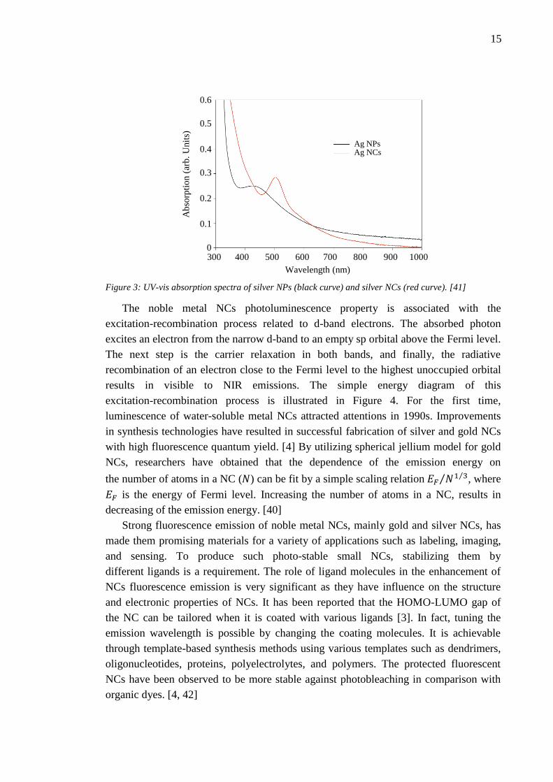
15
Figure 3: UV-vis absorption spectra of silver NPs (black curve) and silver NCs (red curve). [41]
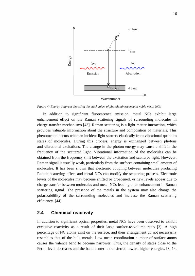
The noble metal NCs photoluminescence property is associated with the
excitation-recombination process related to d-band electrons. The absorbed photon
excites an electron from the narrow d-band to an empty sp orbital above the Fermi level.
The next step is the carrier relaxation in both bands, and finally, the radiative
recombination of an electron close to the Fermi level to the highest unoccupied orbital
results in visible to NIR emissions. The simple energy diagram of this
excitation-recombination process is illustrated in Figure 4. For the first time,
luminescence of water-soluble metal NCs attracted attentions in 1990s. Improvements
in synthesis technologies have resulted in successful fabrication of silver and gold NCs
with high fluorescence quantum yield. [4] By utilizing spherical jellium model for gold
NCs, researchers have obtained that the dependence of the emission energy on
the number of atoms in a NC (𝑁) can be fit by a simple scaling relation 𝐸𝐹 𝑁1 3⁄⁄ , where
𝐸𝐹 is the energy of Fermi level. Increasing the number of atoms in a NC, results in
decreasing of the emission energy. [40]
Strong fluorescence emission of noble metal NCs, mainly gold and silver NCs, has
made them promising materials for a variety of applications such as labeling, imaging,
and sensing. To produce such photo-stable small NCs, stabilizing them by
different ligands is a requirement. The role of ligand molecules in the enhancement of
NCs fluorescence emission is very significant as they have influence on the structure
and electronic properties of NCs. It has been reported that the HOMO-LUMO gap of
the NC can be tailored when it is coated with various ligands [3]. In fact, tuning the
emission wavelength is possible by changing the coating molecules. It is achievable
through template-based synthesis methods using various templates such as dendrimers,
oligonucleotides, proteins, polyelectrolytes, and polymers. The protected fluorescent
NCs have been observed to be more stable against photobleaching in comparison with
organic dyes. [4, 42]
Wavelength (nm)
300 400 500 600 700 800 900 1000
0.6
0.5
0.4
0.3
0.2
0.1
0
Ag NPs Ag NCs
Ab
sorp
tio
n (
arb
. U
nit
s)
16
Figure 4: Energy diagram depicting the mechanism of photoluminescence in noble metal NCs.
In addition to significant fluorescence emission, metal NCs exhibit large
enhancement effect on the Raman scattering signals of surrounding molecules in
charge-transfer mechanisms [43]. Raman scattering is a light-matter interaction, which
provides valuable information about the structure and composition of materials. This
phenomenon occurs when an incident light scatters elastically from vibrational quantum
states of molecules. During this process, energy is exchanged between photons
and vibrational excitations. The change in the photon energy may cause a shift in the
frequency of the scattered light. Vibrational information of the molecules can be
obtained from the frequency shift between the excitation and scattered light. However,
Raman signal is usually weak, particularly from the surfaces containing small amount of
molecules. It has been shown that electronic coupling between molecules producing
Raman scattering effect and metal NCs can modify the scattering process. Electronic
levels of the molecules may become shifted or broadened, or new levels appear due to
charge transfer between molecules and metal NCs leading to an enhancement in Raman
scattering signal. The presence of the metals in the system may also change the
polarizabilility of the surrounding molecules and increase the Raman scattering
efficiency. [44]
2.4 Chemical reactivity
In addition to significant optical properties, metal NCs have been observed to exhibit
exclusive reactivity as a result of their large surface-to-volume ratio [3]. A high
percentage of NC atoms exist on the surface, and their arrangement do not necessarily
resembles that of the bulk metals. Low mean coordination number of surface atoms
causes the valence band to become narrower. Thus, the density of states close to the
Fermi level decreases and the band center is transferred toward higher energies. [3, 14,
Wavenumber
En
ergy
h+
e-
d band
sp band
EFermi
Absorption Emission
hν1 hν
2
17
45] It results in a strong electron affinity and different chemical reactivity from that of
the bulk metals. The electron affinity of metal NCs can be as large as 10 eV while the
highest electron affinity among elements of the periodic table belongs to chlorine which
is 3.61 eV. NCs with such a large electron affinity are called super-halogens and consist
of a metal atom at core enclosed by halogen atoms. A good example of super-halogens
is platinum hexafluoride (PtF6). It is possible to enhance the electron affinity even
further by having a metal atom at core surrounded by super-halogens; these species are
called hyper-halogens. [3]
Interaction of transition metal NCs with molecules such as nitrogen (N2) can be
utilized to investigate the geometry of the NCs. It has been reported that a metal NC
exposed to the gas molecules under a varying pressure can adsorb variable number of
gas molecules. Based on the measurements results, the binding of the cluster and gas
molecule and eventually the structure of the cluster can be determined. [3] Furthermore,
utilizing powerful mass spectrometric techniques enables the accurate examination of
metal NCs reaction with different molecules [46].
Coinage metals are usually considered as catalytically inert materials for lots of
applications. Their low activity in chemical reactions is due to their completely
occupied d-bands leading to higher activation barriers than those for metals with
partially filled d-bands. Nevertheless, NCs of these metals have exhibited high catalytic
activity in many experiments. For instance, high catalytic activity of gold NCs in
reactions such as low temperature CO oxidation and NO reduction has been reported. In
energy structure of low-coordinated coinage metal atoms, there is a narrow gap between
d-band and the Fermi energy level. As a result, the NC surface consists of much more
active sites to adsorb oxygen molecules compared to the closed packed counterparts.
The fraction of surface atoms in the particles strongly depends on their size. Metal NCs
exhibit much more catalytic activity than NPs. Several experiments have been
conducted on Au and Ag NCs and NPs to investigate the influence of metal particles
size on their catalytic activity. [41]
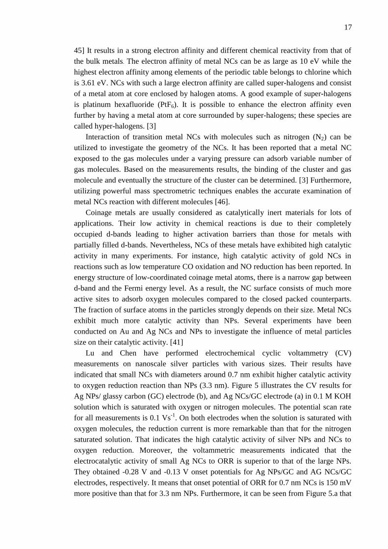
Lu and Chen have performed electrochemical cyclic voltammetry (CV)
measurements on nanoscale silver particles with various sizes. Their results have
indicated that small NCs with diameters around 0.7 nm exhibit higher catalytic activity
to oxygen reduction reaction than NPs (3.3 nm). Figure 5 illustrates the CV results for
Ag NPs/ glassy carbon (GC) electrode (b), and Ag NCs/GC electrode (a) in 0.1 M KOH
solution which is saturated with oxygen or nitrogen molecules. The potential scan rate
for all measurements is 0.1 Vs-1
. On both electrodes when the solution is saturated with
oxygen molecules, the reduction current is more remarkable than that for the nitrogen
saturated solution. That indicates the high catalytic activity of silver NPs and NCs to
oxygen reduction. Moreover, the voltammetric measurements indicated that the
electrocatalytic activity of small Ag NCs to ORR is superior to that of the large NPs.
They obtained -0.28 V and -0.13 V onset potentials for Ag NPs/GC and AG NCs/GC
electrodes, respectively. It means that onset potential of ORR for 0.7 nm NCs is 150 mV
more positive than that for 3.3 nm NPs. Furthermore, it can be seen from Figure 5.a that
18
the oxygen reduction current density at -0.80 V is around -0.25 mA cm-2
for NPs
electrode. However, as shown in Figure 5.b, it increases to -1.50 mA cm-2
at NCs
electrode which is five times higher than the former. Further measurements also resulted
in higher mass activity of small NCs compared to NPs. [41]
Figure 5: Cyclic voltammograms of Ag-NPs/GC (a) and Ag-NCs/GC (b) electrodes in 0.1 M KOH
solutions saturated with nitrogen and oxygen molecules. Current is normalized by electrochemically
active surface areas, and Ag/AgCl was used as the reference. [41]
2.5 Stabilization of metal nanoclusters
As mentioned in chapter 2.1, in order to synthesize metal NCs, a salt or a complex of the
corresponding metal is dissolved in a solvent and reduced to a zero valent state.
However, synthesizing nanoclusters in aqueous solutions is usually difficult because
clusters strongly tend to agglomerate and interact with each other to decrease their
surface energy. It results in the formation of NPs which no longer exhibit molecule-like
properties especially fluorescence emission. [5, 47, 48] Moreover, nucleation of metal
particles is a complicated phenomenon which is a result of cooperation of several
factors such as the difference between the redox potentials of metal salt and the
reducing agent, reaction temperature, rate of addition, and stirring rate. In order to
obtain a monodisperse NC, the nucleation process has to be completed before the
growth stage begins. Therefore, short nucleation time is a requisite. If the nucleation and
growth steps overlap, growth time varies for different nucleation sites, and the result is
N
2 saturated
O2 saturated
(a)
(b)
-1.2 -0.8 -0.4 0 0.4 0.8
0.2
0
-0.2
-0.4
-0.6
0
-0.5
-0.1
-1.5
-2
-2.5
E (V vs Ag/AgCl)
J (m
A c
m-2
)
0
19
an undesired particle size distribution. In order to avoid these phenomena and produce
hydrosol and organosol stable NCs, one needs to stop the growth process at the right
moment to prevent the generation of larger crystals. The growth is stoppable by using
ligand molecules coordinating to the surface atoms. [15] Ligand molecules control the
particle growth thermodynamically rather than kinetically, and may be present in the
solution during the reduction process or added after that [15, 48]. In our case study
which is silver NCs, the former one has been used. Moreover, chemical interaction
between the stabilizer molecules and surface atoms of the metal NCs leads to
considerable effects on the NC electronics structure. Therefore, the nature of the
stabilizer agent controls the fluorescence emission of the protected metal NCs. [47]
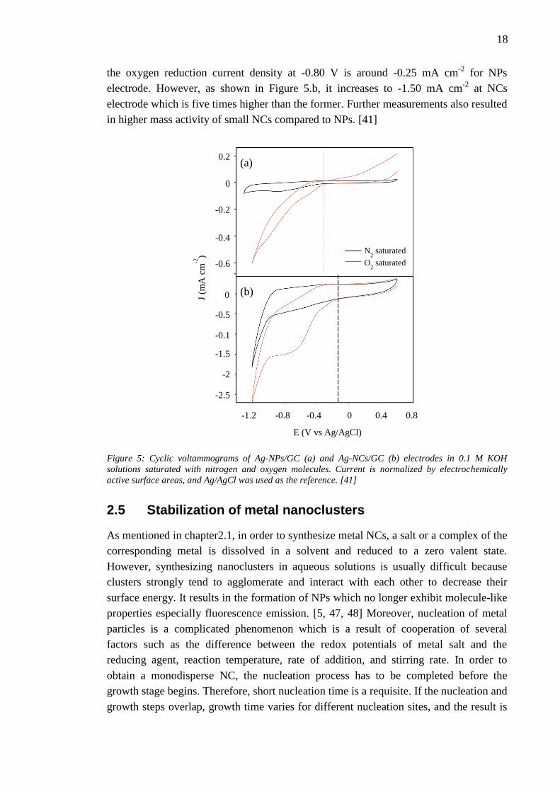
The fundamental cause of NCs aggregation is an attractive vdW force between
particles. Therefore, the stabilization occurs when this attractive force is dominated by a
stronger repulsive one or weakened via covering the NCs. [15] There are different
methods of stabilization depending on the type of the covering layer: electrostatic
(inorganic), steric (organic), and electrosteric stabilizations. Electrostatic stabilization
includes the adsorption of ions to the electrophilic metal surfaces. A created electrical
double layer leads to the Coulombic repulsion force between existed particles.
The electrostatic potential must be high enough to protect particles from aggregation.
Steric stabilization occurs when the metal particle is surrounded by layers of large
organic molecules such as polymers. Polymer stabilizers create abundant weak bonds
with the surface of the NC rather than few strong bonds. Some stabilizers exhibit both
electrostatic and steric effects. That leads to a very reliable process to stabilize NCs.
Electrosteric stabilization includes adsorbing of bulky molecules such as polymers and
surfactants at the NC surface. These molecules shield the particles and at the same time
make strong electrostatic bond to the metal surface. [14, 15] Figure 6 illustrates the
schematic images of electrostatic and steric stabilization methods.
Figure 6: Schematic images of two stabilized particles using (a) electrostatic stabilization, and (b) steric
stabilization by adsorption of polymer molecules [14].
(a) (b)
20
Using the different modes of stabilization, researchers have studied the synthesis of
NCs in a variety of stabilizer agents. One of the mostly used stabilizers is
DNA oligonucleotides, mainly to stabilize silver NCs [47]. For the first time, Dickson
and coworkers reported the synthesis of water-soluble Ag NCs in DNA templates [49,
50]. Since then, lots of studies have been performed on DNA-templated Ag NCs
because of their bright and photostable fluorescence emissions. By utilizing different
DNA sequences, it is possible to tune the fluorescence emission of silver NCs. Proteins
and peptides are another type of protective molecules which enable intercellular
generation of fluorescent noble metal NCs. Furthermore, using dendrimers as stabilizers
have been beneficial because of their uniform composition and structure. The most
commonly used dendrimers are poly-amidoamine (PAMAM) and poly-propyleneimine
(PPI). Recently, using polymer stabilizers have also attracted a lot of attentions. As an
example, Poly-methacrylic acid (PMAA), which is a well-known polymer with
numerous carboxylic acid groups has been proved to be a promising stabilizer for the
formation of stable Ag NCs. Strong affinity of silver ions or silver surfaces to
carboxylic acid groups makes this polymer a unique environment to grow NCs. Other
polymers such as polyethylenimine (PEI), and poly-vinylpyrrolidone (PVP) are also
used as protective ligands. [47] In this thesis, Polyvinyl alcohol (PVA) was used for the
formation and stabilization of water soluble Ag NCs.
The emission spectrum of noble metal NCs is highly affected by the
protective molecules. Therefore, by choosing appropriate stabilizers, the desired
emission of gold and silver NCs for different applications can be obtained. [4] For
instance, it has been reported that quantum confined water-soluble gold NCs stabilized
by PAMAM emit blue light with a high quantum yield [51]. Green and red-emitting
NCs have been also synthesized by tuning the ligand molecules. Le Guevel et al. have
synthesized silver and gold NCs with red emission in bovine serum albumin (BSA)
using wet chemistry [42]. They investigated the influence of pH on growth and emission
of the clusters. Moreover, Ag NCs stabilized by single-strand DNA has been reported to
emit various colors in visible-NIR region [52]. Photogeneration of fluorescent silver
NCs in polymer microgels has been first reported by Kumacheva et al. [53], and was
followed by other researchers to overcome the limitations regarding generation of larger
non-fluorescent nanoparticles. For instance, Shang and Dong used PMAA solution as a
template for the photogeneration of Ag NCs, and they observed obvious color changes
from colorless to dark red in the NCs emissions [17]. Therefore, the emission
wavelength of metal NCs not only is affected by their size, but also depends
significantly on the nature of the encapsulating environment. [4]

21
3. POLYMERS
Polymers are macromolecules that exist in a variety of natural and synthetic forms such
as enzymes, DNA, concretes, plastics, adhesives, coatings, clothes, papers, and are main
ingredients of soil [54]. They are useful materials for most of the recent technologies
mainly because of their large molecular size. When a molecule is large, it includes lots
of intermolecular van der Waals (vdW) contacts to its neighbor molecules. Sum of the
vdW forces keeps molecules tightly together and provides mechanical strength to the
polymeric material. [55] Technologies such as computer chips, portable batteries,
superconductors, optical fibers, liquid crystals, medicines, drug delivery system,
synthetic blood, skin, and limbs use different kinds of polymeric materials [54].
The word ‘polymer’ refers to a chain molecule consisting of structural repeating
units called monomers, which are connected together by covalent bonds through
polymerization process [56]. If the fundamental repeating units comprise a single
identifiable precursor, the polymer is a homopolymer. If a polymer molecule consists
of two or three different types of basic structures, then we have a copolymer. The
composition of copolymers may vary from well-ordered repetition to a random
distribution. The number of repeating units mainly in homopolymer molecules is called
the degree of polymerization (DP). The molecular weight of a polymer MP is then the
molecular weight of the repeating units M0 multiplied by DP, MP=(DP)M0. A polymer
with low molecular weight and low mechanical strength is called oligomer and consists
of at least two monomer units. [55]
Two major factors determining the properties of a polymeric material are the
chemical identity of its monomers and its microstructure. Microstructure is the
arrangement of atoms along the chain that is fixed during the polymerization and cannot
be altered without breaking the covalent bonds. [57] It is formed by a skeleton, which
may have a linear chain, branched chain, or network architecture with lots of atomic
groups attached to the backbone. When each repeating unit of a polymer molecule is
attached to other two repeating units, the molecule is linear. Polystyrene is an example
of linear polymers. If some of the repeating units in the polymer molecule are also
attached to other monomer residues, that are different from the repeating monomers, the
molecule is called branched polymer. For instance, vinyl acetate has such a structure.
By chemically linking linear or branched polymers together, the so-called network
polymers can be obtained. This process is called cross-linking. Finite-sized polymers
also contain some end groups which are different from the repeating structures. Usually,
the exact structure of end groups is not known, and their influence on physical
properties is negligible. [55, 56] The spatial arrangement of a polymer molecule that is
22
determined by the relative location of its monomers is called the polymer conformation.
After the polymerization, a single flexible molecule may embrace various
conformations depending on the flexibility of the chain, and interaction of monomers
with surroundings. [57]
One important classification of polymers related to their structure divides them to
addition molecules and condensation molecules. The repeating unit in condensation
polymers lacks some certain atom(s), which are present in primary monomers building
the polymer molecule. Polyesters or polyamides are examples of condensation
polymers. Addition polymers consist of repeating units with the exact structure of the
monomers. Polyethylene and polyvinyl alcohol are examples of addition polymers.
Condensation polymers are formed through a step-wise polymerization process while
addition polymers are generated by a chain process. [58] A brief explanation of
polymerization processes is presented in 4.1.
If all polymer molecules in a substance contain the same number of monomers, the
polymeric material is monodisperse that is the case for most of the natural polymers
such as proteins. However, synthetic polymers are mainly polydisperse. The
polydispersity of a particular polymer is described by its molar mass distribution
(MMD). [57] The MMD provides information regarding the average molecular size,
and the regularity of the distribution. The chemical structure and the pattern of MMD
control almost all of the other properties of a polymeric material. Some of these
properties such as cohesive forces, packing density, and molecular mobility are directly
affected whereas the others like morphology and relaxation phenomena are indirectly
influenced by chemical structure and MMD. [56]
As mentioned in Chapter 2.4, several polymer molecules provide an appropriate
environment to grow and stabilize nanoclusters. Because of their large molecular
weights, the chain dimensions of polymers are comparable to the range of van der
Waals attractions, and this is useful for steric stabilization methods [59]. In this thesis,
we used polyvinyl alcohol (PVA) as a stabilizer for silver nanoclusters (NCs).
Therefore, in the following subchapters, molecular structure and general properties of
PVA are described, which is followed by polymer processing methods. Finally,
the effects of ambient conditions on polymeric materials are presented.
3.1 Polyvinyl alcohol
Polyvinyl alcohol (PVA) is a synthetic water-soluble resin with excellent film forming,
emulsifying, stabilizing and adhesive properties [60]. The main chain of vinyl polymers
in general contains carbon atoms with single bonds and other additive substituents such
as chlorine, fluorine, or hydroxyl groups [61]. PVA in particular is a linear molecule,
and its relatively simple chemical structure consists of vinyl alcohol (C2H4O) monomer
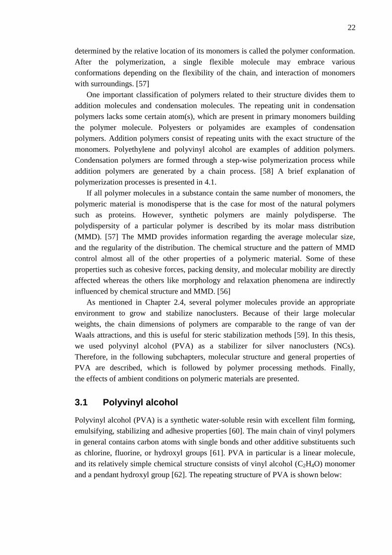
and a pendant hydroxyl group [62]. The repeating structure of PVA is shown below:
23
where m refers to the number of the repeating units [55]. Presence of hydroxyl groups
makes it a hydrophilic polymer [61, 63]. PVA has high biodegradation rate, and the
hydrogen bondings between molecules lead to a high mechanical strength [60, 64]. It
can be well dissolved in water but not in common organic solvents [63]. The viscosity
of aqueous PVA solutions varies with PVA concentration and temperature of the
solution [65].
PVA is synthesized since 1924 when Herman and Haehnel reported the formation of
PVA through saponification of polyvinyl acetate (PVAc). Vinyl alcohol is not a stable
molecule and usually exist in the form of its tautomer, acetaldehyde. Thus, to produce
PVA, first vinyl acetate monomers are polymerized to PVAc; then, it is converted to
PVA through hydrolysis. Sometimes, the hydrolysis does not result in a complete
conversion of PVAc to PVA. Consequently, the produced material is a copolymer of
PVA and PVAc. Various types of PVA grades from partially hydrolyzed to fully
hydrolyzed grades with broad range of MMD are commercially available. The physical
characteristics including water solubility, mechanical strength, gas permeability,
adhesion, diffusion, thermal and stabilizing properties depend significantly on the
crystallinity level of the polymer. Degree of crystallinity is determined by the hydrolysis
level and the average molecular weight of the molecule. Partially hydrolyzed grades
containing residuals of acetate groups exhibit small degrees of crystallinity. It results in
a low strength of the material and high solubility in water compared to fully hydrolyzed
grades. Highly hydrolyzed PVA with degrees of hydrolysis above 98.5% are dissolved
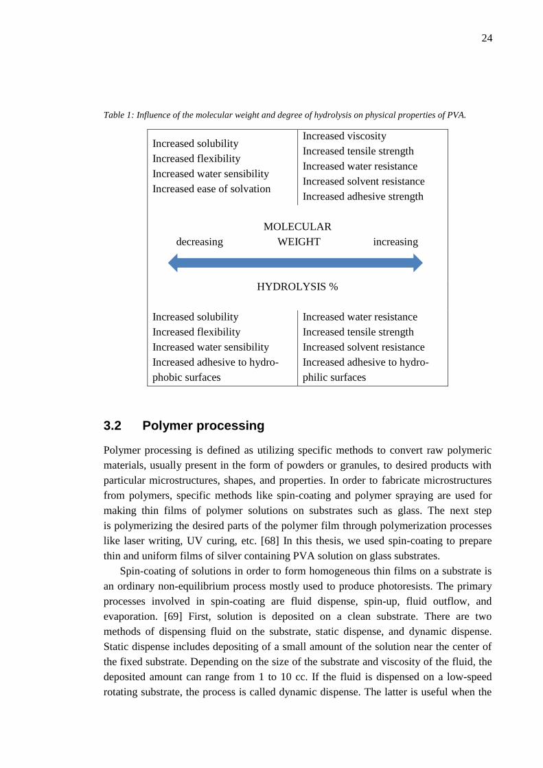
in water if the temperature is well above 70 C. [62, 66] Table 1 provides a summary of
the influence of molecular weight and degree of hydrolysis on physical properties of
PVA.
Features such as aqueous solubility, stabilizing ability, biocompatibility,
biodegradability, non-toxicity, and environmental friendliness make PVA an attractive
material for a variety of applications. It is vastly used in textile industries, paper
products manufacturing, food packaging, adhesives, and coatings. Particularly, it is a
safe polymer for biomedical and pharmaceutical purposes. Moreover, due to its
excellent film-forming properties, PVA is used as high oxygen barrier films,
membranes, and polarizing films. [60, 63, 67]
CH2 C
H
OH
(
)m
24
Table 1: Influence of the molecular weight and degree of hydrolysis on physical properties of PVA.
Increased solubility
Increased flexibility
Increased water sensibility
Increased ease of solvation
Increased viscosity
Increased tensile strength
Increased water resistance
Increased solvent resistance
Increased adhesive strength
decreasing
MOLECULAR
WEIGHT increasing
HYDROLYSIS %
Increased solubility
Increased flexibility
Increased water sensibility
Increased adhesive to hydro-
phobic surfaces
Increased water resistance
Increased tensile strength
Increased solvent resistance
Increased adhesive to hydro-
philic surfaces
3.2 Polymer processing
Polymer processing is defined as utilizing specific methods to convert raw polymeric
materials, usually present in the form of powders or granules, to desired products with
particular microstructures, shapes, and properties. In order to fabricate microstructures
from polymers, specific methods like spin-coating and polymer spraying are used for
making thin films of polymer solutions on substrates such as glass. The next step
is polymerizing the desired parts of the polymer film through polymerization processes
like laser writing, UV curing, etc. [68] In this thesis, we used spin-coating to prepare
thin and uniform films of silver containing PVA solution on glass substrates.
Spin-coating of solutions in order to form homogeneous thin films on a substrate is
an ordinary non-equilibrium process mostly used to produce photoresists. The primary
processes involved in spin-coating are fluid dispense, spin-up, fluid outflow, and
evaporation. [69] First, solution is deposited on a clean substrate. There are two
methods of dispensing fluid on the substrate, static dispense, and dynamic dispense.
Static dispense includes depositing of a small amount of the solution near the center of
the fixed substrate. Depending on the size of the substrate and viscosity of the fluid, the
deposited amount can range from 1 to 10 cc. If the fluid is dispensed on a low-speed
rotating substrate, the process is called dynamic dispense. The latter is useful when the
25
fluid has poor wetting abilities. After deposition of the solution, the next step is spin-up
which includes accelerating the substrate and fluid to a final desired speed. Typically
chosen spin speeds are in the range of 1500-6000 rpm depending on the characteristics
of the fluid and substrate. The spinning speed can last from 10 seconds to several
minutes. It is the cooperation of the spinning speed and spinning time which determine
the final thickness of the layer. Usually, higher speeds and longer time result in thinner
films. The principle of thinning the film during the rotation is that the centrifugal force
spreads the fluid outward and ejects the excess of the liquid out of the edge of the
substrate. Meanwhile, the evaporation of the solvent results in drying the resin,
and consequently increasing the viscosity of the fluid. Viscosity increases up to the
point that the centrifugal force can no longer disperse the resin, and a final equilibrium
thickness is achieved. [70, 71]
Controlling the spin speed is one of the important factors on the layer thickness. It
has influence on both the degree of centrifugal force applied to the resin, and the
velocity and turbulence of the air above the resin. Acceleration of the substrate during
first seconds of spinning also has a significant effect on the film uniformity. It provides
a twisting force to the resin and disperses the fluid around the area. In addition to the
system variables, the nature of the resin is also responsible for the film characteristics.
Properties of the solution such as volatility, viscosity, surface tension, drying rate, and
solid concentration highly affect the drying of the resin and consequently the final
thickness. Ambient conditions such as humidity and temperature of the air around the
solution are other determinant factors. During the process, air flow and turbulence
above the layer has to be minimized or kept constant. It can be achieved by using closed
bowl design spin coaters. This system minimizes the influence of ambient humidity
change and variations of air flow around the substrate. After spinning, if the solvent is a
nonvolatile liquid such as water as in our case, the resin needs to be kept in a desiccator
for final drying. The drying step is essential to stabilize the film before using it. [71]
Finally, a uniform polymer film with a desired thickness is achievable by taking care of
all of the determinant parameters.
After preparing polymer films through spin-coating, the polymer needs to be cured
and hardened through polymerization process. One of the well-known techniques for
microfabrication in polymer films is photo-induced polymerization by using UV curing
or direct laser writing (DLW). The main mechanism of photopolymerization is
photo-induced reaction of monomers or oligomers to produce polymeric materials (this
polymerization method is explained in detail in Chapter 4.) [72]. After fabrication of the
desired structures in polymer films through polymerization step, the unexposed regions
can be washed out by using photoresist developers. [73]
3.3 Effects of ambient conditions on polymeric materials
Particular ambient factors such as heat, light, or chemicals can lead to the
decomposition of a polymer and alter its properties including molecular weight, tensile
26
strength, shape, color, and other important characteristics. Therefore, to have
stable polymeric materials for a long time, one needs to be familiar with the causes of
degradation and their effects on the polymer properties. [74, 75]
Thermal resistance is one of the most important properties of polymers since it
controls the mechanical properties, persistence, spectral stability, and life cycles of
polymers [76]. Even highly resistant polymers may undergo degradation at high
temperatures. At this condition, the primary chemical bonds are broken and polymer
degrades down to its monomers. In principle, thermal degradation can be determined by
dissociation energy of chemical bonds. There are three types of thermal decomposition
mechanisms: chain depolymerization, random decomposition, and degradation through
substituent reactions. Chain depolymerization is the reverse process of chain
polymerization that includes the release of monomer units from one end point of a chain
or at a weak link. Weak links may exist as a result of chain defects or impurities.
Random degradation means the fragmentation at random points along the chain and is
considered as the reverse of polycondensation. The detached segments are usually large
compared to monomer units. Chain and random decompositions may occur separately
or in combination. In the case of vinyl polymers, usually, chain depolymerization is the
dominant degradation process. Degradation by substituent reactions happens through
modification or elimination of substituents, which are connected to the polymer
backbone. For most of the polymers, thermal pyrolysis begins at temperatures around
150-200 C and increases with increasing the temperature. Two major
experimental indices that characterize the thermal degradation are the temperature of
initial decomposition, and the temperature of half decomposition. The initial
decomposition temperature (Td,0) is the temperature at which the weight loss of the
polymeric material due to heating becomes measurable. The temperature of half
decomposition (Td,1/2) is defined as the temperature at which the weight loss reaches the
50% of its ultimate value. These characteristic temperatures depend on the rate of the
heating. According to the reports, Td,0 and Td,1/2 of PVA at a standardized rate of heating
(normally around 3 K/min) are 493 K and 547 K respectively. The characteristic
temperatures change to higher values by increasing the rate of the heating. [74]
Ambient light can be another typical cause of polymer degradation. The
required activation energy to break an individual covalent bond is in the range of
165-420 kJ/mol. That amount of energy corresponds to the wavelengths from 280 nm to
720 nm. Thus, near ultraviolet radiation (300-400 nm) has the adequate amount of
energy to break most of the covalent bonds except very strong ones such as C-H and
O-H. Ideal polymers with perfect structures do not absorb wavelengths longer than 300
nm. However, most of the polymers contain impurities and structural defects
which absorb light, and that results in photochemical degradation when exposed to the
sunlight. The exact nature of the impurities is usually unknown, but it has been accepted
that they are either carbonyl groups or peroxides. UV-induced degradation can be
prevented by utilizing UV-absorbers which transform the absorbed energy into heat, or
by quenchers (for example nickel chelates), which dissipate the electronic excited states
27
of impurities. [74] In addition to UV-radiation, some other sources such as ion
beams, gamma rays, or electron radiation may also be used to degrade polymers for
some purposes [75].
Chemical decomposition may also occur as a result of reactions with surrounding
components. The most important reagent of chemical degradation is oxygen.
Photo-oxidation, caused by radiation, and thermal oxidation, caused by thermal energy
are two primary processes. At room temperatures, the oxidation appears after a long
time because of slow reaction rate. However, factors such as electromagnetic radiation
or thermal energy accelerate the oxidation by formation of radicals. In the case of
photo-oxidation, radical formation occurs through absorption of light photons and in
thermal oxidation through temperature change, shear effects or residues of catalysts.
The rate of thermal oxidation can be estimated by measuring the amount of
oxygen absorption at a particular temperature. Both oxidation processes can be avoided
by using antioxidants. Addition of UV absorbers is also a useful way to prevent
photo-oxidation. In addition to oxidation, other kinds of chemical degradation like
hydrolytic degradation may occur. Hydrolytic degradation takes place when hydrolysis
reactions in water or acids are responsible for breaking the bonds. If the ambient
temperature is high enough, the rate of decomposition is fast. Mechanical properties
including tensile strength, elongation, and impact strength may be destroyed severely as
a result of all chemical degradation processes. In some polymers, it may also lead to
discoloration. [74]
In biological environments, certain micro-organisms and enzymes can motivate the
degradation of polymers. The biodegradability depends on the molecular weight,
molecular structure, and crystallinity of the polymer. The higher the molecular weight,
the lower the biodegradability. Investigations on degradation of PVA in various
environments and conditions have resulted in high degrees of biodegradation, which can
be a desired property for many applications. Among vinyl polymers produced
industrially, PVA is the only one that can undergo degradation by micro-organisms.
[75] The biodegradation of PVA can occur as a result of a random chain division
process in which a two-enzyme catalyzed oxidation is responsible for bond breaking.
[77]
28
4. PHOTOPOLYMERIZATION
Photopolymerization includes a light-induced chain chemical reaction to transfer small
unsaturated molecules in the liquid phase to macromolecules in solid phase within a
polymerizable resin. Different light sources from UV, visible to IR region can be
employed to initiate the polymerization. Fundamental components required for
polymerization are monomers or oligomers in the liquid material. However, direct
formation of reactive species in monomers through light absorption is not an efficient
process. Therefore, presence of photo-initiators (PIs) is required to generate reactive
species, which initiates the polymerization reaction when excited by light.
Photosensitizers (PS) can also be added to extend the spectral sensitivity. They absorb
the incident energy of a wavelength that PI cannot absorb and then transfer the required
excitation energy to the PI. This reaction is called sensitized photo-induced
polymerization. Photo-induced polymerization is commonly considered as an
environmentally friendly technology because of low energy requirements, low-
temperature procedures, and no release of volatile organic compounds. [78, 79]
Photoinitiated polymerization by UV lamps is a well-known method not only for
conventional applications such as adhesives, coating, and inks but also for recent
technologies in photonics, optoelectronics, and microelectromechanical systems
(MEMS). Moreover, due to the developments in laser technology and possibility of high
localization of laser energy, laser-induced polymerization has become an attractive
subject for many scientific areas. This technique has been studied widely for potential
applications in biomedicine, bones and tissue engineering, nanotechnology, direct laser
patterning of microcircuits, holographic devices, information recording media, and so
on. [79, 80, 81] In the following, the principles of photopolymerization process are
explained, that is followed by presenting single-photon and two-photon induced DLW.
4.1 Polymerization processes
Polymerization is a chemical process during which monomers are covalently bonded
together [57]. Two primary mechanisms of polymerization are step-growth and
chain-growth processes [58]. In step-growth mechanism, functional groups of
monomers react with each other in a stepwise process to form dimers, trimers, and other
low molecular weight oligomers to eventually build polymers with high molecular
weights. Sometimes, these stepwise reactions are accompanied by elimination of some
small molecules, which result in the formation of condensation polymers such as
polyesters. [54, 82] Usually, small molecules such as water are released during
condensation polymerization. To reach high molecular weight in this process, an
29
extremely efficient reaction with no side reactions is required. Moreover, molecules
must have at least two reactive functional groups in order to grow through a stepwise
polymerization. Another major mechanism is chain-growth polymerization, which
includes the sequential addition of monomers to the growing chain. Vinyl molecules
such as PVA are usually synthesized via this process. Based on the initiation procedure
and nature of the propagating chain, the chain-growth is classified to anionic, cationic
and free radical processes. [83] The most important process in polymer synthesis is
chain-type radical polymerization. Almost 50% of all synthetic polymers are made
through radical processes. This method is popular because of several reasons including
convenient temperature range (20-100 C) and minimal need for purification of
monomers and solvents. Radical polymerization can be carried out in bulk, solution,
emulsion, aqueous suspensions, and other environments. Another important benefit is
that a large range of monomers can be polymerized using this mechanism. [84] Ionic
type photopolymerizations are not used as commonly as radical type ones. Low curing
speed, low viscosity, small shrinkage after polymerization, and drastic post-irradiation
dark polymerization are some drawbacks of ionic processes. [72]
The primary process in a photo-induced polymerization involves chain-type free
radical reactions. The main steps of chain polymerization are Initiation, Propagation,
and Termination. [72] These processes are explained in detail below.
Quantum yield of photopolymerization is defined by the number ratio of
polymerized monomers to photons required for the polymerization. Ideally, it can reach
several thousand as a result of chain reactions represented by
𝑀𝑀→𝑀2
𝑀→𝑀3⋯𝑀𝑛−1
𝑀→𝑀𝑛 , (15)
where 𝑀 is the monomer unit, and 𝑀𝑛 is the macromolecule contains 𝑛 monomers.
However, in practical systems the quantum yield of monomers and oligomers is small.
By adding PIs, the efficiency of polymerization can be enhanced. PIs are low-weight
light sensitive molecules in the photoresist, which are reduced to initiating radicals
through photon absorption. This process is called ‘photoinitiation’, which is the first and
most important stage of photopolymerization. Initiation process that is used to generate
a radical is defined by
𝑃𝐼ℎ𝜈→ 𝑃𝐼∗→ 𝑅., (16)
where 𝑃𝐼∗, and 𝑅. denote for an intermediate state after absorbing a photon (ℎ𝜈), and
the produced radical, respectively. In many cases, the PI cannot absorb the energy of the
incident light. Instead, light is absorbed by PS molecules and then the energy is
transferred to the PI. In this case, the photoinitiation step is described by the following
reaction: [72]
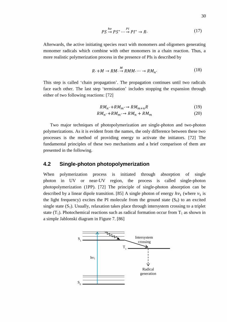
30
𝑃𝑆ℎ𝜈→ 𝑃𝑆∗⋯
𝑃𝐼→ 𝑃𝐼∗ → 𝑅. (17)
Afterwards, the active initiating species react with monomers and oligomers generating
monomer radicals which combine with other monomers in a chain reaction. Thus, a
more realistic polymerization process in the presence of PIs is described by
𝑅.+𝑀 → 𝑅𝑀. 𝑀→ 𝑅𝑀𝑀.⋯ → 𝑅𝑀𝑛. (18)
This step is called ‘chain propagation’. The propagation continues until two radicals
face each other. The last step ‘termination’ includes stopping the expansion through
either of two following reactions: [72]
𝑅𝑀𝑛. +𝑅𝑀𝑚. → 𝑅𝑀𝑚+𝑛𝑅 (19)
𝑅𝑀𝑛. +𝑅𝑀𝑚. → 𝑅𝑀𝑛 + 𝑅𝑀𝑚 (20)
Two major techniques of photopolymerization are single-photon and two-photon
polymerizations. As it is evident from the names, the only difference between these two
processes is the method of providing energy to activate the initiators. [72] The
fundamental principles of these two mechanisms and a brief comparison of them are
presented in the following.
4.2 Single-photon photopolymerization
When polymerization process is initiated through absorption of single
photon in UV or near-UV region, the process is called single-photon
photopolymerization (1PP). [72] The principle of single-photon absorption can be
described by a linear dipole transition. [85] A single photon of energy ℎ𝜈1 (where 𝜈1 is
the light frequency) excites the PI molecule from the ground state (S0) to an excited
single state (S1). Usually, relaxation takes place through intersystem crossing to a triplet
state (T1). Photochemical reactions such as radical formation occur from T1 as shown in
a simple Jablonski diagram in Figure 7. [86]
S1
S0
T1
Intersystem crossing
Radical generation
hν1
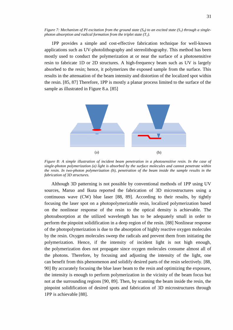
31
Figure 7: Mechanism of PI excitation from the ground state (S0) to an excited state (S1) through a single-
photon absorption and radical formation from the triplet state (T1).
1PP provides a simple and cost-effective fabrication technique for well-known
applications such as UV-photolithography and stereolithography. This method has been
mostly used to conduct the polymerization at or near the surface of a photosensitive
resin to fabricate 1D or 2D structures. A high-frequency beam such as UV is largely
absorbed to the resin; hence, it polymerizes the exposed sample from the surface. This
results in the attenuation of the beam intensity and distortion of the localized spot within
the resin. [85, 87] Therefore, 1PP is mostly a planar process limited to the surface of the
sample as illustrated in Figure 8.a. [85]
Figure 8: A simple illustration of incident beam penetration in a photosensitive resin. In the case of
single-photon polymerization (a) light is absorbed by the surface molecules and cannot penetrate within
the resin. In two-photon polymerization (b), penetration of the beam inside the sample results in the
fabrication of 3D structures.
Although 3D patterning is not possible by conventional methods of 1PP using UV
sources, Maruo and Ikuta reported the fabrication of 3D microstructures using a
continuous wave (CW) blue laser [88, 89]. According to their results, by tightly
focusing the laser spot on a photopolymerizable resin, localized polymerization based
on the nonlinear response of the resin to the optical density is achievable. The
photoabsorption at the utilized wavelength has to be adequately small in order to
perform the pinpoint solidification in a deep region of the resin. [88] Nonlinear response
of the photopolymerization is due to the absorption of highly reactive oxygen molecules
by the resin. Oxygen molecules sweep the radicals and prevent them from initiating the
polymerization. Hence, if the intensity of incident light is not high enough,
the polymerization does not propagate since oxygen molecules consume almost all of
the photons. Therefore, by focusing and adjusting the intensity of the light, one
can benefit from this phenomenon and solidify desired parts of the resin selectively. [88,
90] By accurately focusing the blue laser beam to the resin and optimizing the exposure,
the intensity is enough to perform polymerization in the vicinity of the beam focus but
not at the surrounding regions [90, 89]. Then, by scanning the beam inside the resin, the
pinpoint solidification of desired spots and fabrication of 3D microstructures through
1PP is achievable [88].
(a) (b)
32
Another method that has been vastly used for 3D microfabrication to improve the
spatial resolution in three dimensions is two-photon initiated polymerization [88]. The
principle of two-photon polymerization is described in the next section.
4.3 Two-photon photopolymerization
Two-photon polymerization (2PP) is a localized nonlinear polymerization process
which is used to fabricate polymeric micro/nanostructures by focusing a near-infrared
(NIR) laser beam into photoresists. In this fabrication method, the resin is polymerized
by simultaneous absorption of two photons with almost double wavelength than that
used in 1PP. [72, 91] Two-photon absorption (TPA) was experimentally discovered in
1961 by Kaiser and Garrett though it was theoretically predicted as early as 1931 [92].
For years, it was only used for spectroscopical purposes until its usage for
polymerization induction was reported in 1965 by Pao and Rentzepis [93]. The method
was further developed as a tool for lithographic microfabrication by Kawata’s group in
1997 [94]. In 1990s, the commercialization of femtosecond lasers in addition to
recognition of high-efficiency PIs significantly accelerated the micro/nanofabrication in
solid and liquid media through 2PP. Properties such as ultrashort pulse duration (less
than 5 fs), high beam quality, coherence, substantial nonlinearity, power and frequency
stability, high transient power, and strong localization of femtosecond lasers, have
enabled controllable processing of variety of materials by these lasers. [72, 91] Since
then, this direct laser writing (DLW) technique has been widely applied to fabricate
various photonic, micro-optical, and microchemical components [72].
The principle of TPA is based on the nonlinear response of two-photon transition
rate to the optical intensity [88]. PIs in the ground state (S0) are excited to an excited
state (S1) by simultaneously absorbing two photons, followed by nonradiative
relaxations and radical formation. If the energies of two photons are exactly of the same
amount, this process is called degenerate TPA otherwise it is a non-degenerate one. In
the case of degenerate TPA, equations (16) and (17) can be re-written as:
𝑃𝐼2ℎ𝜈2→ 𝑃𝐼∗→ 𝑅. (21)
𝑃𝑆2ℎ𝜈2→ 𝑃𝑆∗⋯
𝑃𝐼→ 𝑃𝐼∗ → 𝑅. , (22)
where 𝜈2~𝜈1 2⁄ is the photon frequency in two-photon excitation process. To make the
case clear, it can be assumed that when the first photon is absorbed by the molecule, a
virtual intermediate state is created. The lifetime of the virtual state is as short as several
femtoseconds. If the second photon irradiates the molecule before decaying of the
virtual state, TPA happens successfully. This mechanism is called simultaneous TPA. In
addition to simultaneous TPA, there is another mechanism of absorption which is called
stepwise absorption. The requirement for stepwise absorption is the existence of a real
intermediate energy state. First, a population of electrons from the ground state (S0) is
excited to an actual intermediate state (S1) through absorption of the first photon. Then,
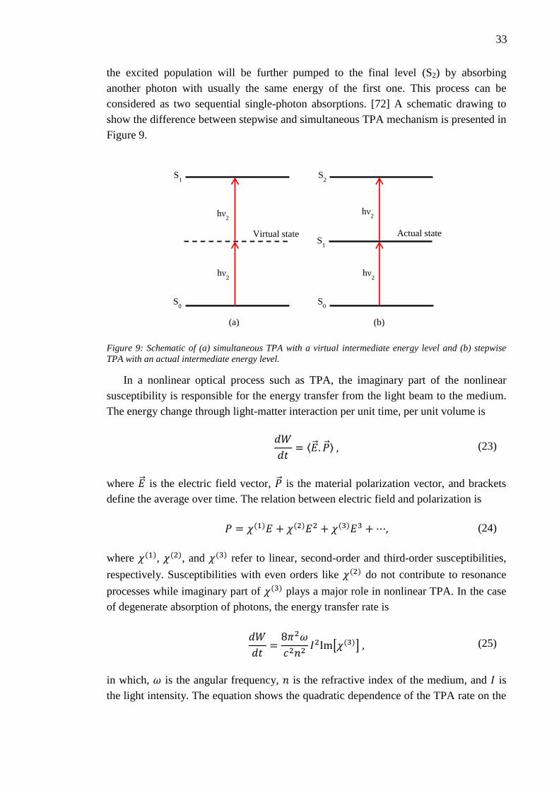
33
the excited population will be further pumped to the final level (S2) by absorbing
another photon with usually the same energy of the first one. This process can be
considered as two sequential single-photon absorptions. [72] A schematic drawing to
show the difference between stepwise and simultaneous TPA mechanism is presented in
Figure 9.
Figure 9: Schematic of (a) simultaneous TPA with a virtual intermediate energy level and (b) stepwise
TPA with an actual intermediate energy level.
In a nonlinear optical process such as TPA, the imaginary part of the nonlinear
susceptibility is responsible for the energy transfer from the light beam to the medium.
The energy change through light-matter interaction per unit time, per unit volume is
𝑑𝑊
𝑑𝑡= ⟨ . ⟩ , (23)
where is the electric field vector, is the material polarization vector, and brackets
define the average over time. The relation between electric field and polarization is
𝑃 = 𝜒(1)𝐸 + 𝜒(2)𝐸2 + 𝜒(3)𝐸3 +⋯, (24)
where 𝜒(1), 𝜒(2), and 𝜒(3) refer to linear, second-order and third-order susceptibilities,
respectively. Susceptibilities with even orders like 𝜒(2) do not contribute to resonance
processes while imaginary part of 𝜒(3) plays a major role in nonlinear TPA. In the case
of degenerate absorption of photons, the energy transfer rate is
𝑑𝑊
𝑑𝑡=8𝜋2𝜔
𝑐2𝑛2𝐼2Im[𝜒(3)] , (25)
in which, 𝜔 is the angular frequency, 𝑛 is the refractive index of the medium, and 𝐼 is
the light intensity. The equation shows the quadratic dependence of the TPA rate on the
S1
S0
Virtual state
hν2
hν2
S2
S0
S1
hν2
hν2
Actual state
(a) (b)
34
light intensity that results in improvement of 3D spatial resolution with better accuracy
than that in conventional single-photon processes. [72]
Most of the resins that are polymerized by UV or visible light exposure in 1PP can
undergo the same reactions when absorbing two photons in 2PP procedure. The only
requirement in the case of 2PP is that the light intensity has to be sufficiently high.
Utilizing pulsed laser technology, it is possible to enhance the energy of a single pulse
to more than four orders of magnitude making the polymerization threshold of any kind
of resin accessible. For instance, the energy of an individual pulse in a
Ti: Sapphire laser amplifier is 1mJ, which is sufficient to polymerize any UV-
polymerizable resin. However, features such as usability, TPA efficiency, tolerance to
variation of exposure dose, and laser-induced breakdown are still material dependence
factors. [72]
A determinant factor in TPA efficiency, is the absorption cross-section 𝛿 which
describes the capability of the sample material to absorb photons, and is defined by
𝛿 =8𝜋2ℎ𝜈2
𝑐2𝑛2𝑁𝐼2Im[𝜒(3)] , (26)
where 𝑁 is the number density of absorbing molecules [72]. Another important
parameter, which effects on TPA efficiency, is the fraction of excitations resulting in
polymer initiation Φ0. In order to obtain efficient absorption and initiation, 𝛿 and Φ0
need to be high enough. This condition can be met by choosing high-efficiency PIs and
radical based polymerization mechanisms. Radical based processes amplify the photo-
induced procedure by adding lots of monomers to the polymer chain in every single
initiation event. [95]
Process of 2PP occurs in a minuscule 3D volume at the focal point, less than
the cubic wavelength (𝜆3). That leads to a unique advantage of 2PP that is high 3D
resolution in polymer resins (Figure 8.b). Another benefit is that the excitation process
is a heat insulating process where the photon energy deposition is so fast that there is
not enough time for electrons to consume it for phonon emissions. This feature is
valuable in photochemical and photophysical reactions where non-localized thermal
effects are undesirable. In addition, polymers usually exhibit negligible linear
absorption in red-NIR regime. It allows the laser beam to penetrate deeply into
the sample and directly induce the polymerization inside the material without disturbing
outside of the focal volume. All of these features make 2PP a beneficial tool for various
applications. [72] However, since TPA has extremely small transition probability, using
a short-pulsed laser source such as Ti: Sapphire is essential, and these sources are
usually expensive compared to conventional CW sources which are used in 1PP.
Therefore, microfabrication through 1PP, using CW lasers with a spatial resolution
comparable to that of 2PP can be more cost-effective for many purposes. [88]
35
5. METHODOLOGY
In this chapter, the experimental methods of fabrication, imaging, and optical
characterization of fluorescent microstructures containing silver NCs in PVA films are
explained. The process of sample preparation in clean room is described in detail. This
is followed by the illustration of custom built setups of direct laser writing (DLW),
bright field microscopy, fluorescence microscopy, and fluorescence spectroscopy of the
microstructures. Finally, the method of atomic force microscopy (AFM) to obtain the
thickness of polymer films and topography of the written structures is presented.
In this thesis, samples were prepared in a clean room located at Optoelectronic
Research Center (ORC) of Tampere University of Technology (TUT). The procedure of
DLW, fluorescent spectroscopy and microscopy was conducted at the Optics
Laboratory of the Department of Physics of TUT. All the AFM measurements and
imaging were performed at Aalto University Nanomicroscopy Center (Aalto-NMC).
5.1 Sample processing
The first step in sample preparation was cleaning the substrates. The substrates used in
the experiments were 170-200 μm thick cover-glasses with 25 mm diameter
manufactured by Electron Microscopy Sciences (EMS). First, the glass coverslips were
wiped by acetone-saturated clothes. To remove the deposited layer of acetone on
coverslips, they were further cleaned by ethanol. Finally, the glass coverslips were
rinsed with Milli-Q (MQ) water with resistivity of 18.2 MΩ.cm and dried with
Nitrogen.
Thin films of PVA containing silver (Ag@PVA) were prepared by spin-coating
aqueous Ag@PVA solutions with different concentrations of silver. The raw polymer
material used in this work was 99% hydrolyzed PVA powder manufactured by
Sigma-Aldrich, and its molecular weight varied between 89000 to 98000 g/mol.
To perform the calculations, we considered a mean value of molecular weight of PVA
that is 93500 g/mol. 3 wt% of PVA aqueous solution was prepared by dissolving 240
mg of PVA powder in 8 ml of MQ water. In order to dissolve PVA with a large degree
of hydrolysis (99%) in water, the liquid was stirred and heated up to 70 C.
Simultaneously, the amounts of 50 mg, 75 mg, 100 mg, 125 mg, and 150 mg of silver
nitrate (AgNO3) powder (169.87 g/mol, Sigma-Aldrich) were weighted and each was
dissolved in 8 ml of MQ water. Then, each one of the aqueous solutions of AgNO3 was
mixed with a 3 wt% PVA solution. Eventually, the final Ag: PVA ratios of 21 wt%, 31
wt%, 42 wt%, 52 wt%, and 62 wt% were obtained. One PVA solution without mixing
36
with AgNO3 was also prepared to ensure that the fluorescence is only originated from
the silver NCs.
The programmable spin coater (OPTIcoat ST 22+, ATMsse) was used to prepare
polymer films from the solutions. First, the spinner was initialized. Then, a clean glass
cover slip was placed on the center of a circular sample holder plate in such a way that
the substrate covered a small vacuum hole in the center of the plate. A regular syringe
was used to pour 500 μl of the Ag@PVA solution on the surface of the substrate. In
order to prevent the formation of air bubbles in the film, the syringe mouth was kept as
close as possible to the substrate without touching it. The spin-coating speed of 1500
rpm, and time of the closed bowl spinning of 120 s were selected from the programs list
on the spin coater. Vacuum was applied to the substrate to keep it constant during spin-
coating. After completion of the spin-coating, the sample was lifted carefully; then, it
was placed inside the nitrogen desiccator cabinet for 12 h to be dried. Care was taken to
minimize the exposure of the ambient light to the sample.
After drying the sample for 12 h in the desiccator, it was mounted on a clean
microscopy slide, using picodent temporary glue, to be prepared for DLW. This
completed the sample preparation process and the sample was placed on a sample
holder of DLW setup for laser exposure.
5.2 Direct laser writing setup
The main components of DLW system are laser source, beam delivery setup, and
specimen mounting components [12]. In this work, a custom-built 1PP setup as shown
in Figure 10 was used to write desired 2D microstructures in Ag@PVA films.
A tunable continuous-wave (CW) single mode diode laser (DL 100, TOPTICA
Photonics) was used as a laser writing source. In all the DLW experiments, we used
laser beam of wavelength 405 nm. The laser power was controlled by a polarizer in
front of the laser source. We performed the DLW with various writing powers in the
range of 50-2000 μW. A combination of two achromatic doublet lenses with focal
lengths of 40 mm and 150 mm was set to collimate the beam and increase its diameter.
Between two lenses of the collimator, a 25 μm pinhole aperture was used to spatially
filter the beam. A spatial filter can provide a clean Gaussian beam with smooth intensity
profile by removing the unwanted high-spatial frequencies of the diffraction pattern and
allowing low spatial frequencies to pass. It can also decrease the additional
spatial noises from the beam. Figure 11 illustrates the combination of a collimator and a
pinhole to obtain a collimated Gaussian beam. We fixed the pinhole on a 30 mm XY
translating lens mount (CXY1, Thorlabs) and adjusted its position precisely at the focal
point of the collimator lenses. An optical beam shutter (SH05, Thorlabs) was placed
after the collimator, and it was controlled by a shutter controller (SC10, Thorlabs). The
shutter can operate in different modes; single, auto, manual, external gate (x gate), and
repeat (REP) modes. In our experiment, we externally provided voltage to control the
opening and closure of the shutter in x gate mode by using DAQx card (NI-6363) and
37
LabVIEW program. A longpass dichroic filter (FF484-FDi01, Semrock) that transmits
wavelengths longer than 484 nm and reflects wavelengths shorter than that, was placed
at 45 degree angle. As we used 405 nm laser beam for DLW, the beam was reflected
towards a 100x, 1.4 NA, oil immersion objective lens (HCX PL APO, Leica).
The objective lens focused the laser beam into the sample, which was mounted in the
three-axis motorized scanning stage (Nanomax, Thorlabs). The diameter of the focused
writing laser spot was around 147 nm calculated by the formula, spot size = 0.51 ×
λDLW/NA. Here, λDLW is the wavelength of the writing laser beam and was 405 nm in
our case. The calculated diameter is the theoretical minimum value of the laser spot if
everything is perfect in the setup. In reality, the laser spot might be in order of 200-250
nm. The 2D structures were written by scanning the sample over the fixed laser beam
with the scanning speed of 5μm/s. The scanning of the sample stage was controlled by a
piezo controller (BPC203, Thorlabs). The piezo controller has three channels to control
the movement of stage in three dimensions, and can operate in closed or open loop
modes. For all the 2D fabrications, two channels of the piezo controller were used in the
closed-loop mode. A data acquisition card (X series DAQ, NI USB-6363) was utilized
to input analog signals to the piezo controller through BNC cables. The output analog
signal from the DAQx card was controlled using a custom-built LabVIEW code.
In-situ imaging of the DLW process was done with a bright field microscope arm
incorporated in the DLW setup. A red light source was adjusted above the sample for
bright-field microscopy. The scattered light from the sample was collected by the
objective lens and transmitted through the dichroic mirror. A 200 mm achromatic
doublet lens was located after the dichroic mirror to focus the light on a CMOS camera
(DCC145M, Thorlabs), or an electron multiplying charge coupled device (EMCCD)
camera (iXon3 897, Andor). A filter (BLP01-488R-25, Semrock) was used before the
camera to prevent transmitting the reflected laser light into the camera.
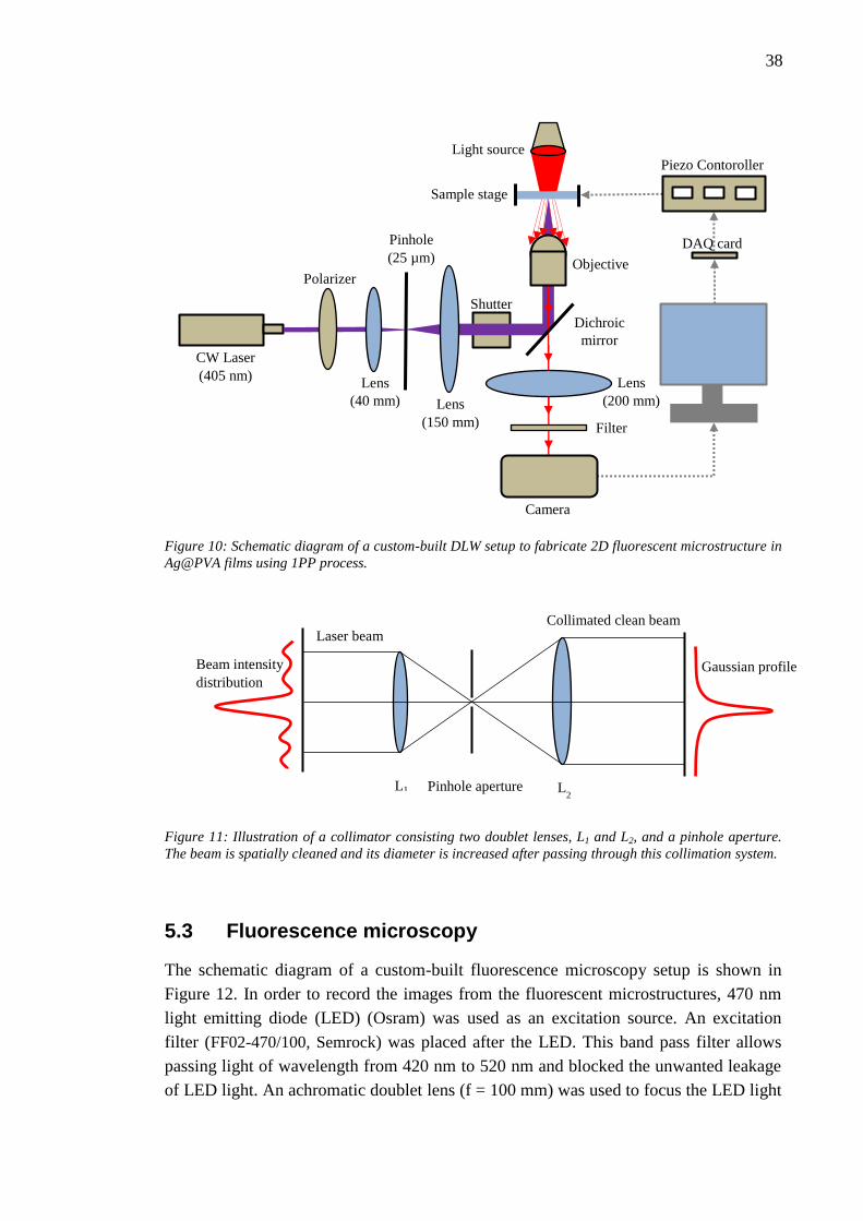
38
Figure 10: Schematic diagram of a custom-built DLW setup to fabricate 2D fluorescent microstructure in
Ag@PVA films using 1PP process.
Figure 11: Illustration of a collimator consisting two doublet lenses, L1 and L2, and a pinhole aperture.
The beam is spatially cleaned and its diameter is increased after passing through this collimation system.
5.3 Fluorescence microscopy
The schematic diagram of a custom-built fluorescence microscopy setup is shown in
Figure 12. In order to record the images from the fluorescent microstructures, 470 nm
light emitting diode (LED) (Osram) was used as an excitation source. An excitation
filter (FF02-470/100, Semrock) was placed after the LED. This band pass filter allows
passing light of wavelength from 420 nm to 520 nm and blocked the unwanted leakage
of LED light. An achromatic doublet lens (f = 100 mm) was used to focus the LED light
Sample stage
CW Laser (405 nm)
Polarizer
Lens (40 mm) Lens
(150 mm)
Pinhole (25 µm)
Shutter
Light source
Objective
Piezo Contoroller
DAQ card
Camera
Lens (200 mm)
Filter
Dichroic
mirror
L1 Pinhole aperture
Laser beam Collimated clean beam
Beam intensity
distribution Gaussian profile
L2
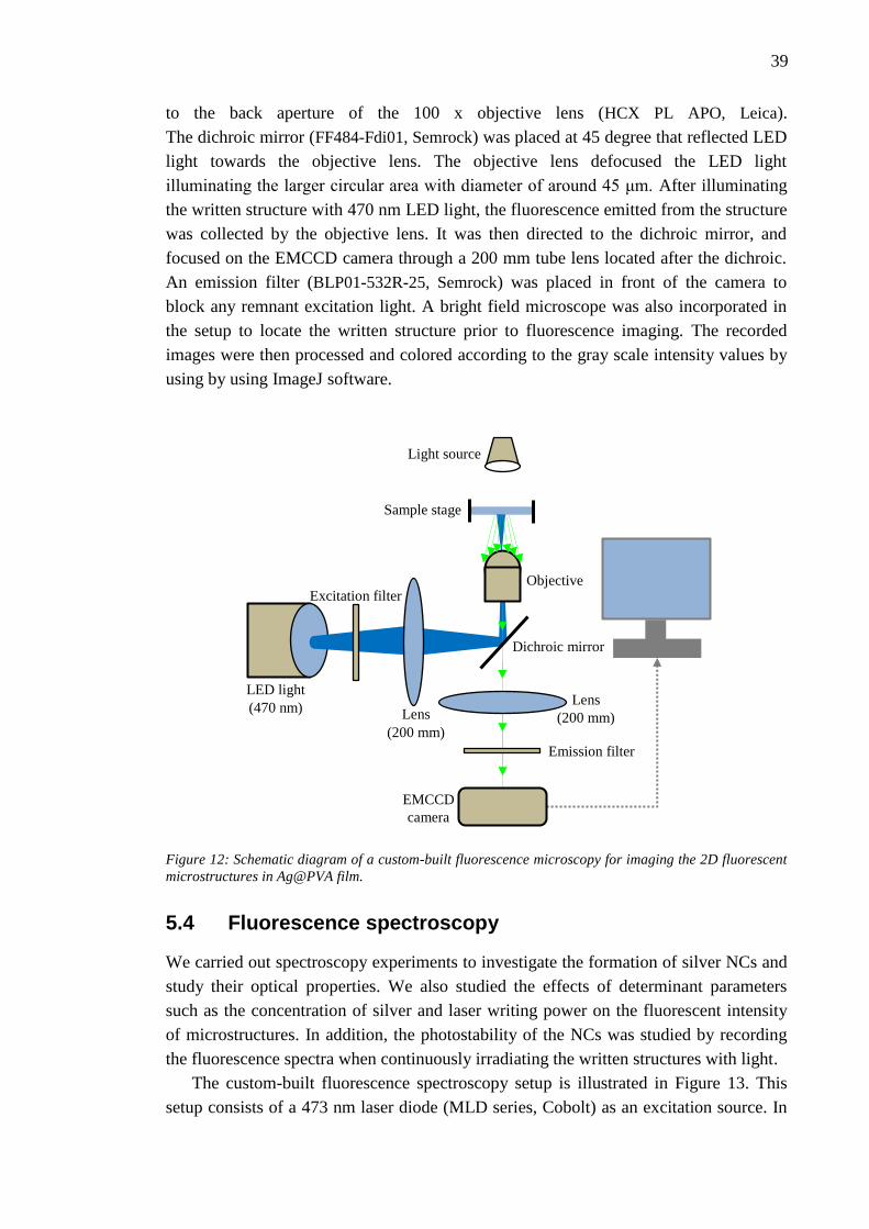
39
to the back aperture of the 100 x objective lens (HCX PL APO, Leica).
The dichroic mirror (FF484-Fdi01, Semrock) was placed at 45 degree that reflected LED
light towards the objective lens. The objective lens defocused the LED light
illuminating the larger circular area with diameter of around 45 μm. After illuminating
the written structure with 470 nm LED light, the fluorescence emitted from the structure
was collected by the objective lens. It was then directed to the dichroic mirror, and
focused on the EMCCD camera through a 200 mm tube lens located after the dichroic.
An emission filter (BLP01-532R-25, Semrock) was placed in front of the camera to
block any remnant excitation light. A bright field microscope was also incorporated in
the setup to locate the written structure prior to fluorescence imaging. The recorded
images were then processed and colored according to the gray scale intensity values by
using by using ImageJ software.
Figure 12: Schematic diagram of a custom-built fluorescence microscopy for imaging the 2D fluorescent
microstructures in Ag@PVA film.
5.4 Fluorescence spectroscopy
We carried out spectroscopy experiments to investigate the formation of silver NCs and
study their optical properties. We also studied the effects of determinant parameters
such as the concentration of silver and laser writing power on the fluorescent intensity
of microstructures. In addition, the photostability of the NCs was studied by recording
the fluorescence spectra when continuously irradiating the written structures with light.
The custom-built fluorescence spectroscopy setup is illustrated in Figure 13. This
setup consists of a 473 nm laser diode (MLD series, Cobolt) as an excitation source. In
LED light (470 nm)
Sample stage
Excitation filter
Light source
Objective
EMCCD camera
Lens (200 mm)
Emission filter
Lens (200 mm)
Dichroic mirror
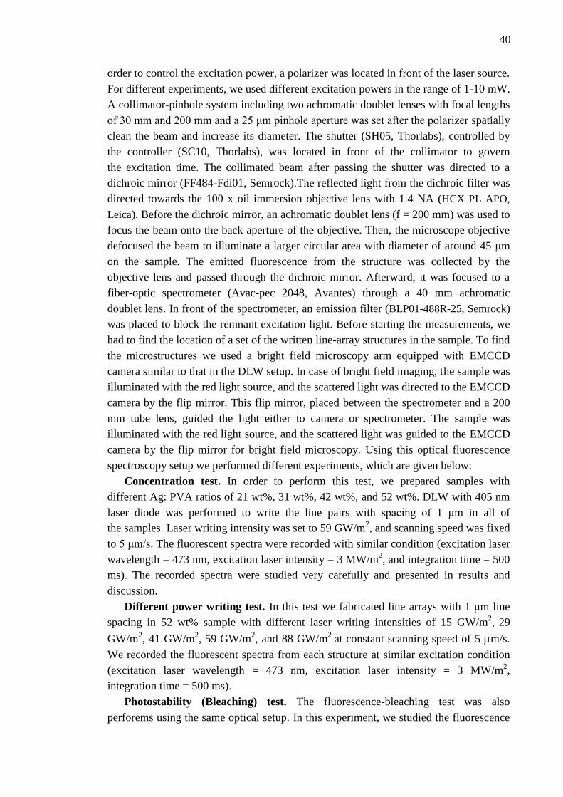
40
order to control the excitation power, a polarizer was located in front of the laser source.
For different experiments, we used different excitation powers in the range of 1-10 mW.
A collimator-pinhole system including two achromatic doublet lenses with focal lengths
of 30 mm and 200 mm and a 25 μm pinhole aperture was set after the polarizer spatially
clean the beam and increase its diameter. The shutter (SH05, Thorlabs), controlled by
the controller (SC10, Thorlabs), was located in front of the collimator to govern
the excitation time. The collimated beam after passing the shutter was directed to a
dichroic mirror (FF484-Fdi01, Semrock).The reflected light from the dichroic filter was
directed towards the 100 x oil immersion objective lens with 1.4 NA (HCX PL APO,
Leica). Before the dichroic mirror, an achromatic doublet lens (f = 200 mm) was used to
focus the beam onto the back aperture of the objective. Then, the microscope objective
defocused the beam to illuminate a larger circular area with diameter of around 45 μm
on the sample. The emitted fluorescence from the structure was collected by the
objective lens and passed through the dichroic mirror. Afterward, it was focused to a
fiber-optic spectrometer (Avac-pec 2048, Avantes) through a 40 mm achromatic
doublet lens. In front of the spectrometer, an emission filter (BLP01-488R-25, Semrock)
was placed to block the remnant excitation light. Before starting the measurements, we
had to find the location of a set of the written line-array structures in the sample. To find
the microstructures we used a bright field microscopy arm equipped with EMCCD
camera similar to that in the DLW setup. In case of bright field imaging, the sample was
illuminated with the red light source, and the scattered light was directed to the EMCCD
camera by the flip mirror. This flip mirror, placed between the spectrometer and a 200
mm tube lens, guided the light either to camera or spectrometer. The sample was
illuminated with the red light source, and the scattered light was guided to the EMCCD
camera by the flip mirror for bright field microscopy. Using this optical fluorescence
spectroscopy setup we performed different experiments, which are given below:
Concentration test. In order to perform this test, we prepared samples with
different Ag: PVA ratios of 21 wt%, 31 wt%, 42 wt%, and 52 wt%. DLW with 405 nm
laser diode was performed to write the line pairs with spacing of 1 μm in all of
the samples. Laser writing intensity was set to 59 GW/m2, and scanning speed was fixed
to 5 μm/s. The fluorescent spectra were recorded with similar condition (excitation laser
wavelength = 473 nm, excitation laser intensity = 3 MW/m2, and integration time = 500
ms). The recorded spectra were studied very carefully and presented in results and
discussion.
Different power writing test. In this test we fabricated line arrays with 1 μm line
spacing in 52 wt% sample with different laser writing intensities of 15 GW/m2, 29
GW/m2, 41 GW/m
2, 59 GW/m
2, and 88 GW/m
2 at constant scanning speed of 5 m/s.
We recorded the fluorescent spectra from each structure at similar excitation condition
(excitation laser wavelength = 473 nm, excitation laser intensity = 3 MW/m2,
integration time = 500 ms).
Photostability (Bleaching) test. The fluorescence-bleaching test was also
perforems using the same optical setup. In this experiment, we studied the fluorescence
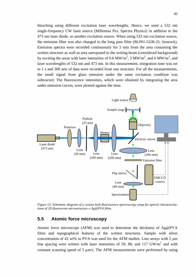
41
bleaching using different excitation laser wavelengths. Hence, we used a 532 nm
single-frequency CW laser source (Millennia Pro, Spectra Physics) in addition to the
473 nm laser diode, as another excitation source. When using 532 nm excitation source,
the emission filter was also changed to the long pass filter (BLP01-532R-25, Semrock).
Emission spectra were recorded continuously for 5 min from the area containing the
written structure as well as area unexposed to the writing beam (considered background)
by exciting the areas with laser intensities of 0.6 MW/m2, 3 MW/m
2, and 6 MW/m
2, and
laser wavelengths of 532 nm and 473 nm. In this measurement, integration time was set
to 1 s and 300 sets of data were recorded from one structure. For all the measurements,
the small signal from glass emission under the same excitation condition was
subtracted. The fluorescence intensities, which were obtained by integrating the area
under emission curves, were plotted against the time.
Figure 13: Schematic diagram of a custom built fluorescence spectroscopy setup for optical characteriza-
tions of 2D fluorescent microstructure o Ag@PVA films.
5.5 Atomic force microscopy
Atomic force microscope (AFM) was used to determine the thickness of Ag@PVA
films and topographical features of the written structures. Sample with silver
concentration of 42 wt% in PVA was used for the AFM studies. Line arrays with 2 μm
line spacing were written with laser intensities of 59, 88, and 117 GW/m2 and with
constant scanning speed of 5 m/s. The AFM measurements were performed by using
Sample stage
Laser diode (473 nm)
Polarizer
Lens (30 mm) Lens
(200 mm)
Pinhole (25 µm)
Shutter
Light source
Objective
EMCCD camera
Lens (200 mm)
Emission filter
Lens (200 mm)
Flip mirror
Dichroic mirror
Spectrometer
Lens (40 mm)
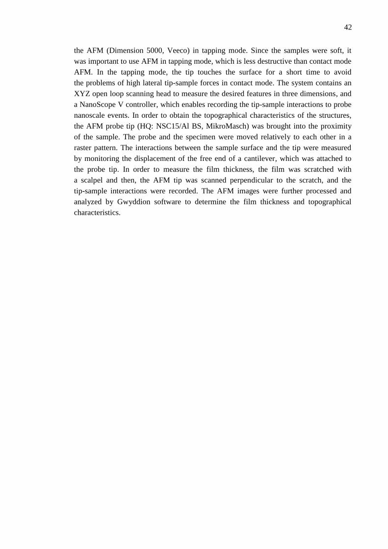
42
the AFM (Dimension 5000, Veeco) in tapping mode. Since the samples were soft, it
was important to use AFM in tapping mode, which is less destructive than contact mode
AFM. In the tapping mode, the tip touches the surface for a short time to avoid
the problems of high lateral tip-sample forces in contact mode. The system contains an
XYZ open loop scanning head to measure the desired features in three dimensions, and
a NanoScope V controller, which enables recording the tip-sample interactions to probe
nanoscale events. In order to obtain the topographical characteristics of the structures,
the AFM probe tip (HQ: NSC15/Al BS, MikroMasch) was brought into the proximity
of the sample. The probe and the specimen were moved relatively to each other in a
raster pattern. The interactions between the sample surface and the tip were measured
by monitoring the displacement of the free end of a cantilever, which was attached to
the probe tip. In order to measure the film thickness, the film was scratched with
a scalpel and then, the AFM tip was scanned perpendicular to the scratch, and the
tip-sample interactions were recorded. The AFM images were further processed and
analyzed by Gwyddion software to determine the film thickness and topographical
characteristics.
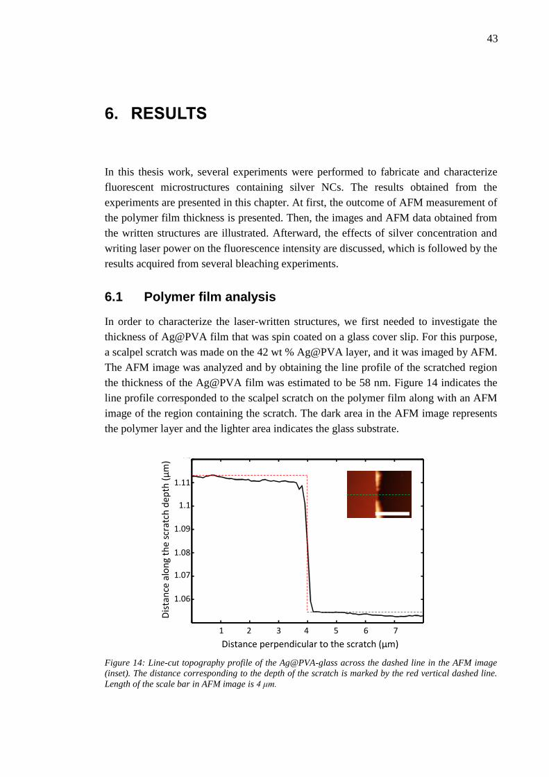
43
6. RESULTS
In this thesis work, several experiments were performed to fabricate and characterize
fluorescent microstructures containing silver NCs. The results obtained from the
experiments are presented in this chapter. At first, the outcome of AFM measurement of
the polymer film thickness is presented. Then, the images and AFM data obtained from
the written structures are illustrated. Afterward, the effects of silver concentration and
writing laser power on the fluorescence intensity are discussed, which is followed by the
results acquired from several bleaching experiments.
6.1 Polymer film analysis
In order to characterize the laser-written structures, we first needed to investigate the
thickness of Ag@PVA film that was spin coated on a glass cover slip. For this purpose,
a scalpel scratch was made on the 42 wt % Ag@PVA layer, and it was imaged by AFM.
The AFM image was analyzed and by obtaining the line profile of the scratched region
the thickness of the Ag@PVA film was estimated to be 58 nm. Figure 14 indicates the
line profile corresponded to the scalpel scratch on the polymer film along with an AFM
image of the region containing the scratch. The dark area in the AFM image represents
the polymer layer and the lighter area indicates the glass substrate.
Figure 14: Line-cut topography profile of the Ag@PVA-glass across the dashed line in the AFM image
(inset). The distance corresponding to the depth of the scratch is marked by the red vertical dashed line.
Length of the scale bar in AFM image is 4 μm.
1.11
1.1
1.09
1.08
1.07
1.06
Dis
tan
ce a
lon
g th
e sc
ratc
h d
epth
(μ
m)
Distance perpendicular to the scratch (μm)
1 2 3 4 5 6 7
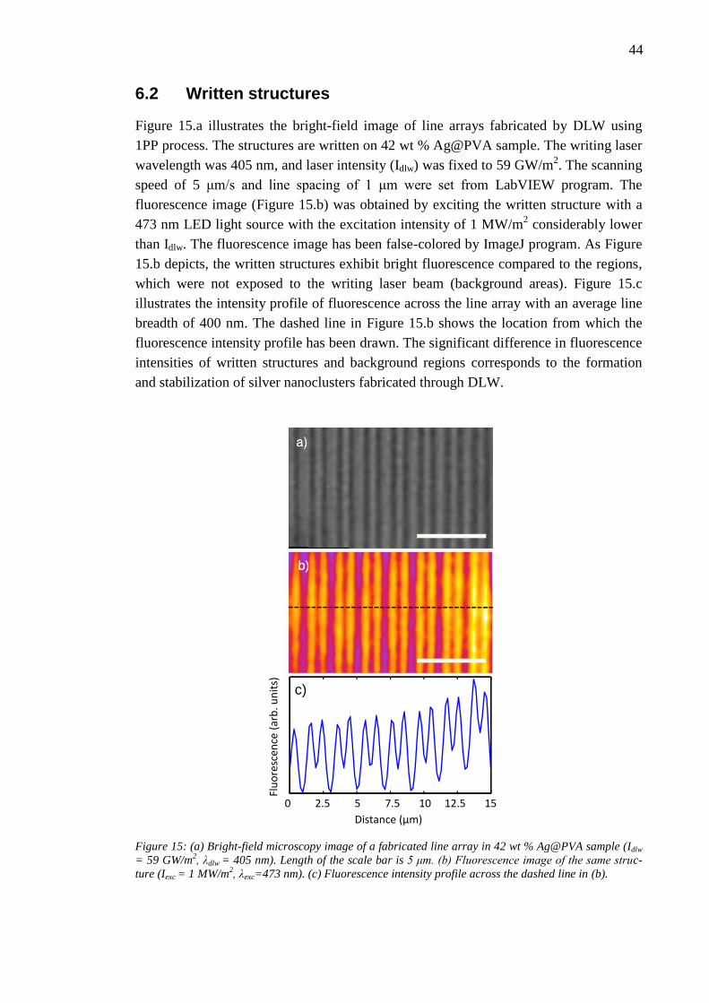
44
6.2 Written structures
Figure 15.a illustrates the bright-field image of line arrays fabricated by DLW using
1PP process. The structures are written on 42 wt % Ag@PVA sample. The writing laser
wavelength was 405 nm, and laser intensity (Idlw) was fixed to 59 GW/m2. The scanning
speed of 5 μm/s and line spacing of 1 μm were set from LabVIEW program. The
fluorescence image (Figure 15.b) was obtained by exciting the written structure with a
473 nm LED light source with the excitation intensity of 1 MW/m2 considerably lower
than Idlw. The fluorescence image has been false-colored by ImageJ program. As Figure
15.b depicts, the written structures exhibit bright fluorescence compared to the regions,
which were not exposed to the writing laser beam (background areas). Figure 15.c
illustrates the intensity profile of fluorescence across the line array with an average line
breadth of 400 nm. The dashed line in Figure 15.b shows the location from which the
fluorescence intensity profile has been drawn. The significant difference in fluorescence
intensities of written structures and background regions corresponds to the formation
and stabilization of silver nanoclusters fabricated through DLW.
Figure 15: (a) Bright-field microscopy image of a fabricated line array in 42 wt % Ag@PVA sample (Idlw
= 59 GW/m2, λdlw = 405 nm). Length of the scale bar is 5 μm. (b) Fluorescence image of the same struc-
ture (Iexc = 1 MW/m2, λexc=473 nm). (c) Fluorescence intensity profile across the dashed line in (b).
Distance (μm)
Flu
ore
scen
ce (
arb
. un
its)
c)
0 2.5 5 7.5 10 12.5 15
45
Moreover, the detailed analysis of the written structures on 42% Ag@PVA samples
was performed through AFM characterization. The AFM results indicated the formation
of grooves in the exposed areas. Figure 16 shows the AFM images of the structures
written with different Idlw and the corresponding line profiles along the marked regions.
The represented line profiles are the results of averaging over 15 profiles obtained from
each AFM image. The depths in line profiles manifest the formation of 3D grooves at
the positions of the laser-written structures. The depths and widths of the grooves were
extracted from the profiles, and the mean values were calculated for each structure. The
depths of the grooves made by laser intensities of 59 GW/m2, 88 GW/m
2, and 117
GW/m2
were measured to be 32 nm, 35 nm, and 38 nm, respectively. The corresponding
values of the widths were found to be around 377, 600, and 700 nm, respectively.
Figure 16: AFM images of the structures written with Idlw of a) 59 GW/m
2, b) 88 GW/m
2, and c) 117
GW/m2 in 42 wt % Ag@PVA samples (left). Length of the scale bar is 5 μm. Line-cut topography profiles
of the structures across the dashed lines (right). For clarity, the line profiles of a) and b) have been
vertically shifted by 40 and 20 nm, respectively.
6.3 Effect of silver concentration
To investigate the origin of the fluorescence emitted from the written structures in
Ag@PVA films, we performed the DLW experiment on samples with different
Ag/PVA weight ratios (0% to 62%). For all the experiments, the writing laser intensity
and the scanning speed were fixed to Idlw = 59 GW/m2, and 5 μm/s respectively. For
PVA films without silver, we could not visualize changes caused by this laser intensity
or even higher intensities. Therefore, we skipped that sample from further spectroscopy
measurements. The fluorescence emission spectra from other samples were recorded by
exposing the written structures to the 473 nm laser beam. The excitation power of the
laser was set to 3 MW/m2
and samples were exposed to the beam for 500 ms. The weak
fluorescence spectrum emitted from the glass substrate was subtracted from all the
measured spectra. The result of the concentration test is illustrated in Figure 17.
It indicates that the fluorescence intensity increases with increasing the silver
concentration. Dependence of the fluorescence signal on the silver concentration
confirms that the fluorescence is due to the silver NCs in PVA films. Moreover, the
c)
b)
a) 40 30 20 10
0 -10 -20 -30 -40
Distance perpendicular to the grooves (μm) 2 4 6 8 10 12 14
Dis
tan
ce f
rom
th
e fi
lm le
vel (
nm
)
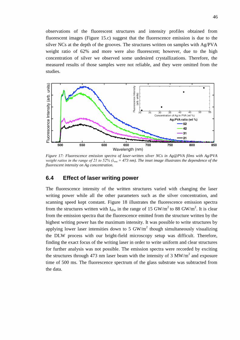
46
observations of the fluorescent structures and intensity profiles obtained from
fluorescent images (Figure 15.c) suggest that the fluorescence emission is due to the
silver NCs at the depth of the grooves. The structures written on samples with Ag/PVA
weight ratio of 62% and more were also fluorescent; however, due to the high
concentration of silver we observed some undesired crystallizations. Therefore, the
measured results of those samples were not reliable, and they were omitted from the
studies.
Figure 17: Fluorescence emission spectra of laser-written silver NCs in Ag@PVA films with Ag/PVA
weight ratios in the range of 21 to 52% (λexc = 473 nm). The inset image illustrates the dependence of the
fluorescent intensity on Ag concentration.
6.4 Effect of laser writing power
The fluorescence intensity of the written structures varied with changing the laser
writing power while all the other parameters such as the silver concentration, and
scanning speed kept constant. Figure 18 illustrates the fluorescence emission spectra
from the structures written with Idlw in the range of 15 GW/m2
to 88 GW/m2. It is clear
from the emission spectra that the fluorescence emitted from the structure written by the
highest writing power has the maximum intensity. It was possible to write structures by
applying lower laser intensities down to 5 GW/m2 though simultaneously visualizing
the DLW process with our bright-field microscopy setup was difficult. Therefore,
finding the exact focus of the writing laser in order to write uniform and clear structures
for further analysis was not possible. The emission spectra were recorded by exciting
the structures through 473 nm laser beam with the intensity of 3 MW/m2 and exposure
time of 500 ms. The fluorescence spectrum of the glass substrate was subtracted from
the data.
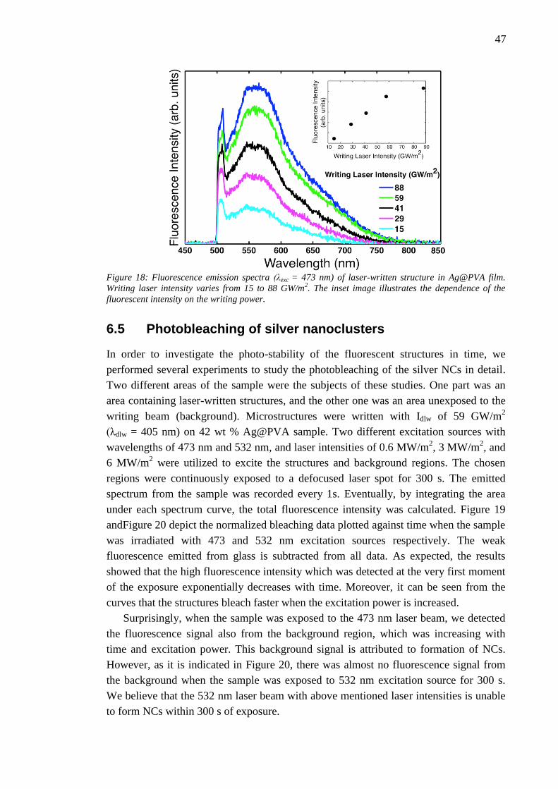
47
Figure 18: Fluorescence emission spectra (λexc = 473 nm) of laser-written structure in Ag@PVA film.
Writing laser intensity varies from 15 to 88 GW/m2. The inset image illustrates the dependence of the
fluorescent intensity on the writing power.
6.5 Photobleaching of silver nanoclusters
In order to investigate the photo-stability of the fluorescent structures in time, we
performed several experiments to study the photobleaching of the silver NCs in detail.
Two different areas of the sample were the subjects of these studies. One part was an
area containing laser-written structures, and the other one was an area unexposed to the
writing beam (background). Microstructures were written with Idlw of 59 GW/m2
(λdlw = 405 nm) on 42 wt % Ag@PVA sample. Two different excitation sources with
wavelengths of 473 nm and 532 nm, and laser intensities of 0.6 MW/m2, 3 MW/m
2, and
6 MW/m2 were utilized to excite the structures and background regions. The chosen
regions were continuously exposed to a defocused laser spot for 300 s. The emitted
spectrum from the sample was recorded every 1s. Eventually, by integrating the area
under each spectrum curve, the total fluorescence intensity was calculated. Figure 19
andFigure 20 depict the normalized bleaching data plotted against time when the sample
was irradiated with 473 and 532 nm excitation sources respectively. The weak
fluorescence emitted from glass is subtracted from all data. As expected, the results
showed that the high fluorescence intensity which was detected at the very first moment
of the exposure exponentially decreases with time. Moreover, it can be seen from the
curves that the structures bleach faster when the excitation power is increased.
Surprisingly, when the sample was exposed to the 473 nm laser beam, we detected
the fluorescence signal also from the background region, which was increasing with
time and excitation power. This background signal is attributed to formation of NCs.
However, as it is indicated in Figure 20, there was almost no fluorescence signal from
the background when the sample was exposed to 532 nm excitation source for 300 s.
We believe that the 532 nm laser beam with above mentioned laser intensities is unable
to form NCs within 300 s of exposure.
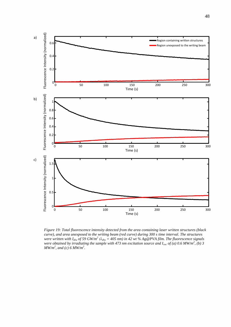
48
Figure 19: Total fluorescence intensity detected from the area containing laser written structures (black
curve), and area unexposed to the writing beam (red curve) during 300 s time interval. The structures
were written with Idlw of 59 GW/m2 (λdlw = 405 nm) in 42 wt % Ag@PVA film. The fluorescence signals
were obtained by irradiating the sample with 473 nm excitation source and Iexc of (a) 0.6 MW/m2, (b) 3
MW/m2, and (c) 6 MW/m
2.
0 50 100 150 200 250 300
0.6
0.4
0.2
0
Flu
ore
scen
ce I
nte
nsi
ty (
no
rmal
ized
)
Time (s)
0 50 100 150 200 250 300 Time (s)
1
0.8
0.6
0.4
0.2
0
Flu
ore
scen
ce I
nte
nsi
ty (
no
rmal
ized
)
0 50 100 150 200 250 300 Time (s)
1.5
1
0.5
0
Flu
ore
scen
ce I
nte
nsi
ty (
no
rmal
ized
)
Region containing written structures
Region unexposed to the writing beam
a)
b)
c)
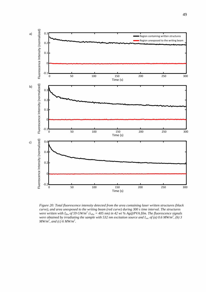
49
Figure 20: Total fluorescence intensity detected from the area containing laser written structures (black
curve), and area unexposed to the writing beam (red curve) during 300 s time interval. The structures
were written with Idlw of 59 GW/m2 (λdlw = 405 nm) in 42 wt % Ag@PVA film. The fluorescence signals
were obtained by irradiating the sample with 532 nm excitation source and Iexc of (a) 0.6 MW/m2, (b) 3
MW/m2, and (c) 6 MW/m
2.
0 50 100 150 200 250 300
0.3
0.2
0.1
0
-0.1
Flu
ore
scen
ce I
nte
nsi
ty (
no
rmal
ized
)
Time (s)
Region containing written structures Region unexposed to the writing beam
0 50 100 150 200 250 300 Time (s)
0.3
0.2
0.1
0
-0.1
Flu
ore
scen
ce I
nte
nsi
ty (
no
rmal
ized
)
0 50 100 150 200 250 300 Time (s)
0.6
0.4
0.2
0
-0.2
Flu
ore
scen
ce I
nte
nsi
ty (
no
rmal
ized
)
a)
b)
c)
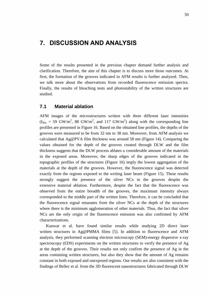
50
7. DISCUSSION AND ANALYSIS
Some of the results presented in the previous chapter demand further analysis and
clarification. Therefore, the aim of this chapter is to discuss more those outcomes. At
first, the formation of the grooves indicated in AFM results is further analyzed. Then,
we talk more about the observations from recorded fluorescence emission spectra.
Finally, the results of bleaching tests and photostability of the written structures are
studied.
7.1 Material ablation
AFM images of the microstructures written with three different laser intensities
(Idlw = 59 GW/m2, 88 GW/m
2, and 117 GW/m
2) along with the corresponding line
profiles are presented in Figure 16. Based on the obtained line profiles, the depths of the
grooves were measured to be from 32 nm to 38 nm. Moreover, from AFM analysis we
calculated that Ag@PVA film thickness was around 58 nm (Figure 14). Comparing the
values obtained for the depth of the grooves created through DLW and the film
thickness suggests that the DLW process ablates a considerable amount of the materials
in the exposed areas. Moreover, the sharp edges of the grooves indicated in the
topographic profiles of the structures (Figure 16) imply the lowest aggregation of the
materials at the depth of the grooves. However, the fluorescence signal was detected
exactly from the regions exposed to the writing laser beam (Figure 15). These results
strongly suggest the presence of the silver NCs in the grooves despite the
extensive material ablation. Furthermore, despite the fact that the fluorescence was
observed from the entire breadth of the grooves, the maximum intensity always
corresponded to the middle part of the written lines. Therefore, it can be concluded that
the fluorescence signal emanates from the silver NCs at the depth of the structures
where there is the minimum agglomeration of other materials. Thus, the fact that silver
NCs are the only origin of the fluorescence emission was also confirmed by AFM
characterizations.
Kunwar et al. have found similar results while studying 2D direct laser
written structures in Ag@PMMA films [5]. In addition to fluorescence and AFM
analysis, they performed scanning electron microscopy (SEM)-energy dispersive x-ray
spectroscopy (EDS) experiments on the written structures to verify the presence of Ag
at the depth of the grooves. Their results not only confirm the presence of Ag in the
areas containing written structures, but also they show that the amount of Ag remains
constant in both exposed and unexposed regions. Our results are also consistent with the
findings of Bellec et al. from the 3D fluorescent nanostructures fabricated through DLW
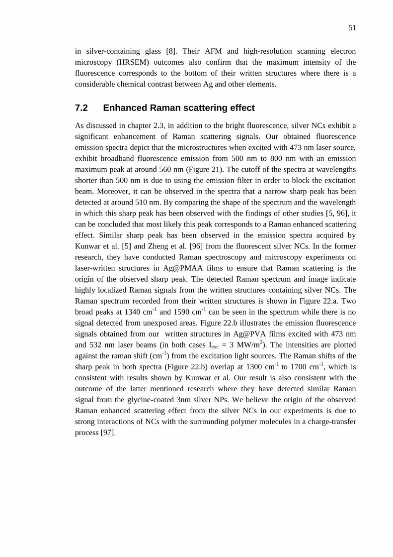
51
in silver-containing glass [8]. Their AFM and high-resolution scanning electron
microscopy (HRSEM) outcomes also confirm that the maximum intensity of the
fluorescence corresponds to the bottom of their written structures where there is a
considerable chemical contrast between Ag and other elements.
7.2 Enhanced Raman scattering effect
As discussed in chapter 2.3, in addition to the bright fluorescence, silver NCs exhibit a
significant enhancement of Raman scattering signals. Our obtained fluorescence
emission spectra depict that the microstructures when excited with 473 nm laser source,
exhibit broadband fluorescence emission from 500 nm to 800 nm with an emission
maximum peak at around 560 nm (Figure 21). The cutoff of the spectra at wavelengths
shorter than 500 nm is due to using the emission filter in order to block the excitation
beam. Moreover, it can be observed in the spectra that a narrow sharp peak has been
detected at around 510 nm. By comparing the shape of the spectrum and the wavelength
in which this sharp peak has been observed with the findings of other studies [5, 96], it
can be concluded that most likely this peak corresponds to a Raman enhanced scattering
effect. Similar sharp peak has been observed in the emission spectra acquired by
Kunwar et al. [5] and Zheng et al. [96] from the fluorescent silver NCs. In the former
research, they have conducted Raman spectroscopy and microscopy experiments on
laser-written structures in Ag@PMAA films to ensure that Raman scattering is the
origin of the observed sharp peak. The detected Raman spectrum and image indicate
highly localized Raman signals from the written structures containing silver NCs. The
Raman spectrum recorded from their written structures is shown in Figure 22.a. Two
broad peaks at 1340 cm-1
and 1590 cm-1
can be seen in the spectrum while there is no
signal detected from unexposed areas. Figure 22.b illustrates the emission fluorescence
signals obtained from our written structures in Ag@PVA films excited with 473 nm
and 532 nm laser beams (in both cases Iexc = 3 MW/m2). The intensities are plotted
against the raman shift (cm-1
) from the excitation light sources. The Raman shifts of the
sharp peak in both spectra (Figure 22.b) overlap at 1300 cm-1
to 1700 cm-1
, which is
consistent with results shown by Kunwar et al. Our result is also consistent with the
outcome of the latter mentioned research where they have detected similar Raman
signal from the glycine-coated 3nm silver NPs. We believe the origin of the observed
Raman enhanced scattering effect from the silver NCs in our experiments is due to
strong interactions of NCs with the surrounding polymer molecules in a charge-transfer
process [97].
52
Figure 21: Emission spectrum (λexc = 473 nm) obtained from fluorescent microstructures. Inset image
illustrates the fluorescence image of the written structures. Length of the scale bar is 5 μm.
Figure 22: (a) Raman spectra detected from the written structures (black) in Ag@PMMA thin film, and
unexposed areas (red) [5]. (b) Emission spectra detected from the written structures in Ag@PVA thin film
excited with 473 nm (blue), and 532 nm (red) as a function of the Raman shift from the excitation light.
450 500 550 600 650 700 750 800 850
Fl
uo
resc
ence
Inte
nsi
ty (
arb
. un
its)
Wavelength (nm)
250
200
150
100
Wavenumber (cm-1
)
1800 1600 1400 1200 1000 800
Inte
nsi
ty (
cou
nts
)
Written structures
Unexposed area
Flu
ore
sce
nce
Inte
nsi
ty (
arb
. un
its)
0 2000 4000 6000 8000
Wavenumber (cm-1
)
Excitation wavelength (nm) 473 532
a)
b)
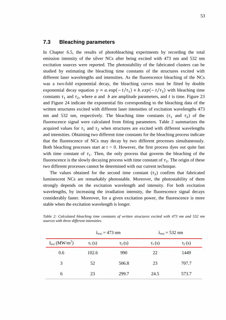
53
7.3 Bleaching parameters
In Chapter 6.5, the results of photobleaching experiments by recording the total
emission intensity of the silver NCs after being excited with 473 nm and 532 nm
excitation sources were reported. The photostability of the fabricated clusters can be
studied by estimating the bleaching time constants of the structures excited with
different laser wavelengths and intensities. As the fluorescence bleaching of the NCs
was a two-fold exponential decay, the bleaching curves must be fitted by double
exponential decay equation 𝑦 = 𝑎. exp(− 𝑡 𝜏1⁄ ) + 𝑏. 𝑒𝑥𝑝(− 𝑡 𝜏2⁄ ) with bleaching time
constants 𝜏1 and 𝜏2, where 𝑎 and 𝑏 are amplitude parameters, and 𝑡 is time. Figure 23
and Figure 24 indicate the exponential fits corresponding to the bleaching data of the
written structures excited with different laser intensities of excitation wavelengths 473
nm and 532 nm, respectively. The bleaching time constants (𝜏1 and 𝜏2) of the
fluorescence signal were calculated from fitting parameters. Table 2 summarizes the
acquired values for 𝜏1 and 𝜏2 when structures are excited with different wavelengths
and intensities. Obtaining two different time constants for the bleaching process indicate
that the fluorescence of NCs may decay by two different processes simultaneously.
Both bleaching processes start at t = 0. However, the first process dyes out quite fast
with time constant of 𝜏1. Then, the only process that governs the bleaching of the
fluorescence is the slowly decaying process with time constant of 𝜏2. The origin of these
two different processes cannot be determined with our current technique.
The values obtained for the second time constant (𝜏2) confirm that fabricated
luminescent NCs are remarkably photostable. Moreover, the photostability of them
strongly depends on the excitation wavelength and intensity. For both excitation
wavelengths, by increasing the irradiation intensity, the fluorescence signal decays
considerably faster. Moreover, for a given excitation power, the fluorescence is more
stable when the excitation wavelength is longer.
Table 2: Calculated bleaching time constants of written structures excited with 473 nm and 532 nm
sources with three different intensities.
λexc = 473 nm λexc = 532 nm
Iexc (MW/m2) τ1 (s) τ2 (s) τ1 (s) τ2 (s)
0.6
3
6
102.6
52
23
990
506.8
299.7
22
23
24.5
1449
707.7
573.7
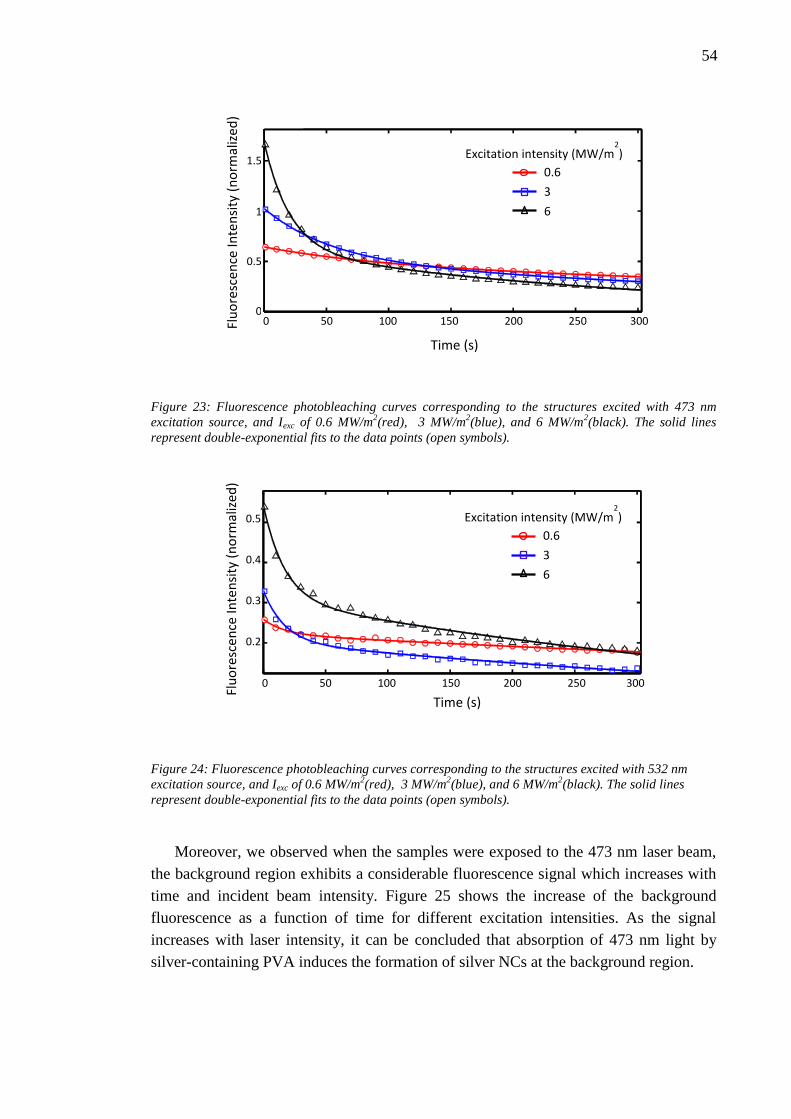
54
Figure 23: Fluorescence photobleaching curves corresponding to the structures excited with 473 nm
excitation source, and Iexc of 0.6 MW/m2(red), 3 MW/m
2(blue), and 6 MW/m
2(black). The solid lines
represent double-exponential fits to the data points (open symbols).
Figure 24: Fluorescence photobleaching curves corresponding to the structures excited with 532 nm
excitation source, and Iexc of 0.6 MW/m2(red), 3 MW/m
2(blue), and 6 MW/m
2(black). The solid lines
represent double-exponential fits to the data points (open symbols).
Moreover, we observed when the samples were exposed to the 473 nm laser beam,
the background region exhibits a considerable fluorescence signal which increases with
time and incident beam intensity. Figure 25 shows the increase of the background
fluorescence as a function of time for different excitation intensities. As the signal
increases with laser intensity, it can be concluded that absorption of 473 nm light by
silver-containing PVA induces the formation of silver NCs at the background region.
0 50 100 150 200 250 300
Time (s)
Excitation intensity (MW/m2)
0.6
3
6
1.5
1
0.5
0
Flu
ore
sce
nce
Inte
nsi
ty (
no
rmal
ized
)
0 50 100 150 200 250 300
Time (s)
0.5
0.4
0.3
0.2
Flu
ore
sce
nce
Inte
nsi
ty (
no
rmal
ized
)
Excitation intensity (MW/m2)
0.6
3
6
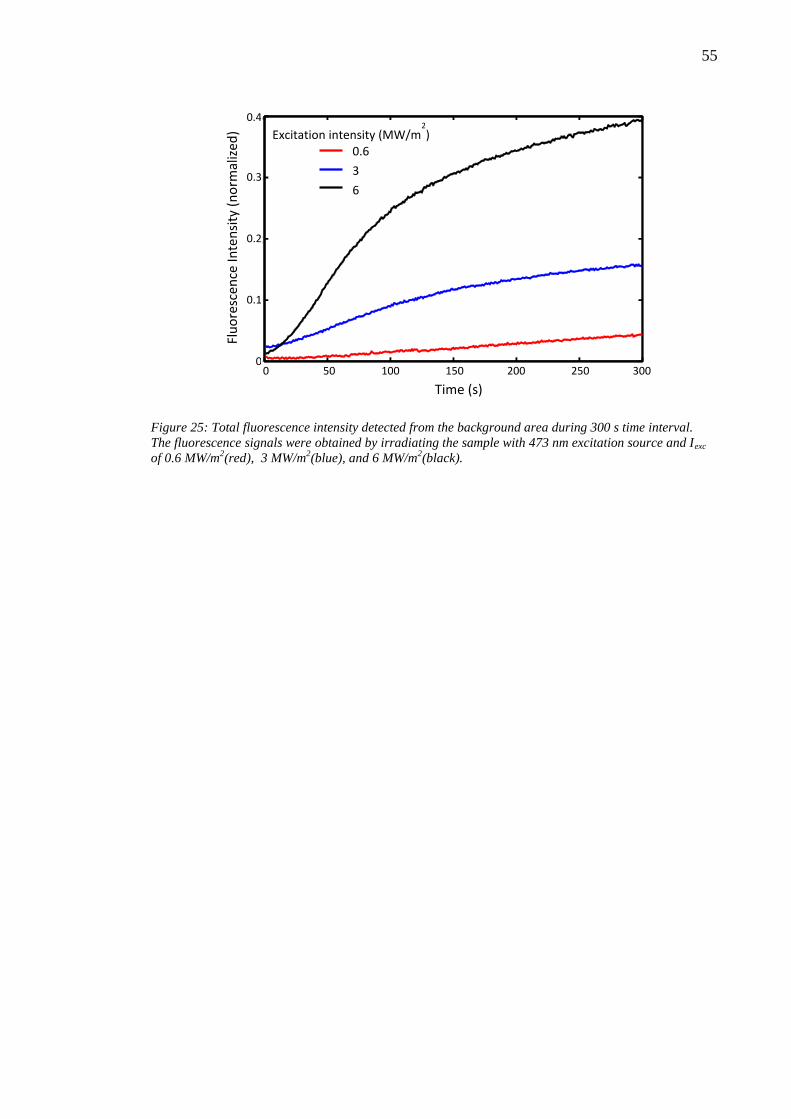
55
Figure 25: Total fluorescence intensity detected from the background area during 300 s time interval.
The fluorescence signals were obtained by irradiating the sample with 473 nm excitation source and Iexc
of 0.6 MW/m2(red), 3 MW/m
2(blue), and 6 MW/m
2(black).
Time (s)
0 50 100 150 200 250 300
0.4
0.3
0.2
0.1
0
Flu
ore
sce
nce
Inte
nsi
ty (
no
rmal
ized
) Excitation intensity (MW/m2)
0.6
3
6

56
8. CONCLUSION
Nanoclusters as an intermediate state between atoms and nanoparticles exhibit
significant optical, electronic, and chemical properties, which have made them attractive
subjects of many studies during last decades. In this work, the major characteristics of
metal nanoclusters with a focus on significant optical properties of noble metal NCs
were studied. The physical principles of cluster growth and the need for stabilizing them
in order to make benefit from their unique properties were described. Different modes
of cluster stabilization by utilizing various stabilizing matrices were introduced
and compared. Then, we focused on the features of polymers since they have been
known as excellent stabilizers of colloids and clusters for a variety of applications.
Notably, properties of PVA, the polymer matrix we utilized to grow and stabilize silver
NCs, were explained. Physical process of polymerization and more specifically single
and two-photon photo-induced polymerization techniques were introduced and
compared.
Two-dimensional fluorescent microstructures with submicron line widths were
fabricated by stabilizing silver NCs in silver containing PVA films utilizing
single-photon DLW process using tightly focused beam of a 405 nm CW diode laser.
Thin films of Ag@PVA with various concentrations of silver were prepared on glass
substrates through spin-coating, and microstructures were written with different
scanning speeds and laser writing intensities. Characterization of the samples was
performed using AFM, bright-field microscopy, fluorescence microscopy, and
fluorescence spectroscopy.
The thickness measurements of Ag@PVA films and fabricated structures indicated
that DLW ablates a significant amount of material in the exposed areas. However, the
obtained fluorescence profiles suggested that despite the material removal, silver NCs
remain at the depth of the structures as the origin of the luminescence. Dependence of
the fluorescence intensity emitted from the structures on the silver concentration was
another evidence that the luminescence is due to the silver NCs stabilized by polymer
molecules. Increasing the writing intensity showed the increment in line-width of the
written microstructures, and consequently, enhancement of the total fluorescence
intensity from the NCs. Along with the broadband fluorescence emission, a sharp peak
was detected which is most likely attributed to an enhanced Raman scattering effect.
Photostability of NCs was studied through several photobleaching tests, which were
performed by irradiating the sample for 300 s and simultaneously recording the
fluorescence intensity. Two different bleaching rates were observed indicated that the
fluorescence decay is affected by two processes. The time constant corresponding to the
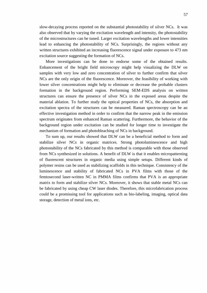
57
slow-decaying process reported on the substantial photostability of silver NCs. It was
also observed that by varying the excitation wavelength and intensity, the photostability
of the microstructures can be tuned. Larger excitation wavelengths and lower intensities
lead to enhancing the photostability of NCs. Surprisingly, the regions without any
written structures exhibited an increasing fluorescence signal under exposure to 473 nm
excitation source suggesting the formation of NCs.
More investigations can be done to endorse some of the obtained results.
Enhancement of the bright field microscopy might help visualizing the DLW on
samples with very low and zero concentration of silver to further confirm that silver
NCs are the only origin of the fluorescence. Moreover, the feasibility of working with
lower silver concentrations might help to eliminate or decrease the probable clusters
formation in the background region. Performing SEM-EDS analysis on written
structures can ensure the presence of silver NCs in the exposed areas despite the
material ablation. To further study the optical properties of NCs, the absorption and
excitation spectra of the structures can be measured. Raman spectroscopy can be an
effective investigation method in order to confirm that the narrow peak in the emission
spectrum originates from enhanced Raman scattering. Furthermore, the behavior of the
background region under excitation can be studied for longer time to investigate the
mechanism of formation and photobleaching of NCs in background.
To sum up, our results showed that DLW can be a beneficial method to form and
stabilize silver NCs in organic matrices. Strong photoluminescence and high
photostability of the NCs fabricated by this method is comparable with those observed
from NCs synthesized in solutions. A benefit of DLW is that it enables micropatterning
of fluorescent structures in organic media using simple setups. Different kinds of
polymer resins can be used as stabilizing scaffolds in this technique. Consistency of the
luminescence and stability of fabricated NCs in PVA films with those of the
femtosecond laser-written NC in PMMA films confirms that PVA is an appropriate
matrix to form and stabilize silver NCs. Moreover, it shows that stable metal NCs can
be fabricated by using cheap CW laser diodes. Therefore, this microfabrication process
could be a promissing tool for applications such as bio-labeling, imaging, optical data
storage, detection of metal ions, etc.
58
REFERENCES
[1] C. N. R. Rao, A. Müller and A. K. Cheetham, "Nanomaterials-an Introduction," in
The Chemistry of Nanomaterials, John Wiley & Sons, 2006, pp. 1-11.
[2] H.-T. Sun and Y. Sakka, "Luminescent Metal Nanoclusters: Controlled Synthesis
and Functional Applications," Sci. Technol. Adv. Mater, vol. 15, no. 1, 2014.
[3] P. Jena and A. W. Castleman Jr., "Introduction to Atomic Clusters," in
Nanoclusters, Elsevier, 2010, pp. 1-28.
[4] C.-A. J. Lin, C.-H. Lee, J.-T. Hsieh, H.-H. Wang, J. K. Li, J.-L. Shen, W.-H. Chan,
H.-I. Yeh and W. H. Chang, "Synthesis of Fluorescent Metallic Nanoclusters
toward Biomedical Application: Recent Progress and Present Challenges," Journal
of Medical and Biological Engineering, vol. 29, pp. 276-283, 2009.
[5] P. Kunwar, J. Hassinen, G. Bautista, R. H. A. Ras and J. Toivonen, "Direct Laser
Writing of Photostable Fluorescent Silver Nanoclusters in Polymer Films," ACS
Nano, vol. 8, p. 11165–11171, 2014.
[6] J. Zheng, J. T. Petty and R. M. Dickson, "High Quantum Yield Blue Emission from
Water-Soluble Au8 Nanodots," J. Am. Chem. Soc., vol. 125, no. 26, p. 7780–7781,
2003.
[7] E. G. Gwinn, P. O'Neill, A. J. Guerrero, D. Bouwmeester and D. K. Fygenson,
"Sequence-Dependent Fluorescence of DNA-Hosted Silver," Adv. Mater, vol. 20,
pp. 279-283, 2008.
[8] M. Bellec, A. Royon, K. Bourhis, J. Choi, B. Bousquet, M. Treguer, T. Cardinal,
J.-J. Videau, M. Richardson and L. Canioni, "3D Patterning at the Nanoscale of
Fluorescent Emitters in Glass," J. Phys. Chem. C, vol. 114, pp. 15584-15588, 2010.
[9] G. De Cremer, B. F. Sels, J.-i. Hotta, M. . B. J. Roeffaers, E. Bartholomeeusen, E.
Coutiño-Gonzalez, V. Valtchev, D. E. De Vos, T. Vosch and J. Hofkens, "Optical
Encoding of Silver Zeolite Microcarriers," Advanced Materials, vol. 22, no. 9, p.
59
957–960, 2010.
[10] T. Linnert, P. Mulvaney, A. Henglein and H. WeUer, "Long-Lived Nonmetallic
Silver Clusters in Aqueous Solution: Preparation and Photolysis," J. Am. Chem.
Soc, vol. 112, p. 46574664 , 1990.
[11] H. Xu and K. S. Suslick, "Water-Soluble Fluorescent Silver Nanoclusters,"
Advanced Materials, vol. 22, pp. 1078-1082, 2010.
[12] C. B. Arnold and A. Piqué, "Laser Direct-Write Processing," MRS BULLETIN ,
vol. 32, pp. 9-15, 2007.
[13] I. Diez and R. H. A. Ras, "Fluorescent Silver Nanoclusters," Nanoscale, vol. 3, pp.
1963-1970, 2011.
[14] J. D. Aiken III and R. G. Finke, "A Review of Modern Transition-metal
Nanoclusters: Their Synthesis, Characterization, and Applications in Catalysis,"
Journal of Molecular Catalysis A: Chemical, vol. 145, pp. 1-44, 1999.
[15] H. Bönnemann and K. S. Nagabhushana, "Metal Nanoclusters: Synthesis and
Strategies," in Metal Nanoclusters in Catalysis and Materials Science, Elsevier
B.V., 2008, pp. 21-26.
[16] M. Faraday, "Experimental Relations of Gold (and other Metals) to Light," The
Royal Society, vol. 147, pp. 145-181, 1857.
[17] L. Shang and S. Dong, "Facile Preparation of Water-soluble Fluorescent Silver
Nanoclusters Using a Polyelectrolyte Template," Chem. Commun, no. 9, p. 1088–
1090, 2008.
[18] M. S. El-Shall and A. S. Edelstein, "Formation of Clusters and Nanoparticles from
a Supersaturated Vapor and Selected Properties," in Nanomaterials: Synthesis,
Properties and Applications, Taylor & Francis Group, 1996, pp. 13-20.
[19] T. A. Ring, "Nano-sized Cluster Nucleation," Advances in Colloid and Interface
Science, vol. 91, pp. 473-499, 2001.
[20] A. Fischer, R. Pagni, R. Compton and D. Kondepudi, "Laser Induced
Crystallization," in Nanoclusters, Elsevier, 2010, pp. 343-356.
60
[21] H. M. Helmy, C. Ballhaus, R. O. Fonseca, R. Wirth, N. Thorsten and M. Tredoux,
"Noble Metal Nanoclusters and Nanoparticles," Nature Communications, vol. 4,
2013.
[22] V. K. LaMer and R. H. Dinegar, "Theory, Production and Mechanism of Formation
of Monodispersed Hydrosols," J. Am. Chem. Soc., vol. 72, p. 4847–4854, 1950.
[23] J. Turkevich, P. C. Stevenson and J. Hillier, "A Study of the Nucleation and
Growth Processes in the Synthesis of Colloidal Gold," Discuss. Faraday Soc., vol.
11, pp. 55-75, 1951.
[24] A. E. Nielsen, Kinetics of Precipitation, Pergamon Press, 1964.
[25] E. E. Finney and R. G. Finke, "Nanocluster Nucleation and Growth Kinetic and
Mechanistic Studies: A Review Emphasizing Transition-metal Nanoclusters,"
Journal of Colloid and Interface Science, vol. 317, p. 351–374, 2008.
[26] G. Schmid, in Clusters and Colloids: From Theory to Applications, John Wiley &
Sons, 2008, pp. 1-6.
[27] G. Schmid, "General Features of Metal Nanoparticles Physics," in Metal
Nanoclusters in Catalysis and Materials Science, Elsevier, 2008, pp. 3-19.
[28] L. J. De Jongh, "Metal-cluster Compounds: Model Systems for Nanosized Metal
Particles," Applied Organometallic Chemistry , vol. 12, pp. 393-399, 1998.
[29] G. Schmid, "Quantum Dots," in Nanoparticles, Wiley-VCH, 2010, pp. 6-19.
[30] E. U. Rafailov, "Quantum Dot Technologies," in The Physics and Engineering of
Compact Quantum Dot-based Lasers for Biophotonics, Wiley-VCH, 2014, p. 8.
[31] F. Janetzko, A. Goursot, T. Mineva, P. Calaminici, R. Flores-Moreno, A. M.
Köster and D. R. Salahub, "Cluster Structures: Bridging Experiment and Theory,"
in Nanoclusters, Elsevier B.V., 2010, pp. 152-153.
[32] J. A. Alonso, "Electronic and Atomic Structure, and Magnetism of Transition-
Metal Clusters," Chemical Reviews, vol. 100, pp. 637-677, 2000.
[33] O. Cheshnovsky, K. J. Taylor, J. Conceicao and R. E. Smalley, "Ultraviolet
61
Photoelectron Spectra of Mass-selected Copper Clusters: Evolution of the 3d
Band," Phys. Rev. Lett., vol. 64, pp. 1785-1788, 1990.
[34] N. Fujima and T. Yamaguchi, "Shell Model and Magnetism of Transition-metal
Microclusters," Journal of Non-Crystalline Solids, Vols. 117-118, pp. 285-288,
1990.
[35] C. Massobrio, A. Pasquarello and R. Car, "Structural and Electronic Properties Of
Small Copper Clusters - A First Principles Study," Chemical Physics Letters, vol.
238, pp. 215-221, 1995.
[36] C. W. J. Bauschlicher, S. R. Langhoff and H. Partridge, "Theoretical Study of the
Homonuclear Tetramers and Pentamers of the Group 1B Metals (Cu, Ag, and Au),"
J. Chem. Phys., vol. 93, pp. 8133-8137, 1990.
[37] K. Michaelian, N. Rendón and I. L. Garzón, "Structure and Energetics of Ni, Ag,
and Au Nanoclusters," Phys. Rev. B, vol. 60, pp. 2000-2010, 1999.
[38] D. L. Fedlheim and C. A. Foss, in Metal Nanoparticles: Synthesis,
Characterization, and Applications, CRC Press, 2001, pp. 1-22.
[39] R. H. Magruder III, L. Yang, R. F. Haglund Jr., C. W. White, L. Yang, R.
Dorsinville and R. R. Alfano, "Optical Properties of Gold Nanocluster Composites
Formed by Deep Ion Implantation in Silica," Applied Physics Letters, vol. 62, pp.
1730-1732, 1993.
[40] J. Zheng, C. Zhang and R. M. Dickson, "Highly Fluorescent,Water-Soluble, Size-
Tunable Gold Quantum Dots," Physical Review Letters, vol. 93, 2004.
[41] Y. Lu and W. Chen, "Size Effect of Silver Nanoclusters on Their Catalytic Activity
for Oxygen Electro-reduction," Journal of Power Sources, vol. 197, pp. 107-110,
2012.
[42] X. Le Guevel, B. Hötzer, G. Jung, K. Hollemeyer, V. Trouillet and M. Schneider,
"Formation of Fluorescent Metal (Au, Ag) Nanoclusters Capped in Bovine Serum
Albumin Followed by Fluorescence and Spectroscopy," Phys. Chem. C, vol. 115,
p. 10955–10963, 2011.
[43] J. Zheng, Y. Ding, B. Tian, Z. L. Wang and X. Zhuang, "Luminescent and Raman
Active Silver Nanoparticles with Polycrystalline," J. AM. CHEM. SOC., vol. 130,
62
p. 10472–10473, 2008.
[44] K. Kneipp, "Surface-enhanced Raman Scattering," Physics Today, vol. 31, pp. 40-
46, 2007.
[45] F. Klasovsky and P. Claus, "Metal Nanoclusters in Catalysis: Effects of
Nanoparticle Size, Shape, and Structure," in Metal Nanoclusters in Catalysis and
Materials Science, Elsevier B.V. , 2007, pp. 167-177.
[46] P. B. Armentrout, "Reactivity and Thermochemistry of Transition Metal Cluster
Cations," in Nanoclusters, Elsevier B.V., 2010, pp. 269-270.
[47] J. Li, J.-J. Zhu and K. Xu, "Fluorescent Metal Nanoclusters: From Synthesis to
Applications," Trends in Analytical Chemistry, vol. 58, pp. 90-98, 2014.
[48] G. Schmid and L. F. Chi, "Metal Clusters and Colloids," Advanced Materials, vol.
10, pp. 515-526, 1998.
[49] J. T. Petty, J. Zheng, N. V. Hud and R. M. Dickson, "DNA-Templated Ag
Nanocluster Formation," J. AM. CHEM. SOC. 2, vol. 126, pp. 5207-5212, 2004.
[50] T. Vosch, Y. Antoku, J.-C. Hsiang, C. I. Richards, J. I. Gonzalez and R. M.
Dickson, "Strongly Emissive Individual DNA-encapsulated Ag Nanoclusters as
Single-molecule Fluorophores," Proceedings of the National Academy of Sciences
of the United States of America, vol. 104, pp. 12616-12621, 2007.
[51] Y. Bao, C. Zhong, D. M. Vu, J. P. Temirov, R. B. Dyer and J. S. Martinez,
"Nanoparticle-Free Synthesis of Fluorescent Gold Nanoclusters at Physiological
Temperature," J. Phys. Chem. C, vol. 111, pp. 12194-12198, 2007.
[52] C. I. Richards, S. Choi, J.-C. Hsiang, Y. Antoku, T. Vosch, A. Bongiorno, Y.-L.
Tzeng and R. M. Dickson, "Oligonucleotide-Stabilized Ag Nanocluster
Fluorophores," J. AM. CHEM. SOC., vol. 130, p. 5038–5039, 2008.
[53] J. Zhang, S. Xu and E. Kumacheva, "Photogeneration of Fluorescent Silver
Nanoclusters in Polymer Microgels," Advanced Materials, vol. 17, pp. 2336-2340,
2005.
[54] C. E. Carraher, "Introduction to Polymer Science and Technology," in Applied
Polymer Science: 21st Century, Elsevier, 2000, pp. 21-26.
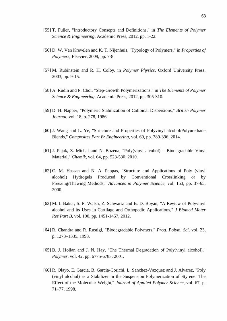
63
[55] T. Fuller, "Introductory Consepts and Definitions," in The Elements of Polymer
Science & Engineering, Academic Press, 2012, pp. 1-22.
[56] D. W. Van Krevelen and K. T. Nijenhuis, "Typology of Polymers," in Properties of
Polymers, Elsevier, 2009, pp. 7-8.
[57] M. Rubinstein and R. H. Colby, in Polymer Physics, Oxford University Press,
2003, pp. 9-15.
[58] A. Rudin and P. Choi, "Step-Growth Polymerizations," in The Elements of Polymer
Science & Engineering, Academic Press, 2012, pp. 305-310.
[59] D. H. Napper, "Polymeric Stabilization of Colloidal Dispersions," British Polymer
Journal, vol. 18, p. 278, 1986.
[60] J. Wang and L. Ye, "Structure and Properties of Polyvinyl alcohol/Polyurethane
Blends," Composites Part B: Engineering, vol. 69, pp. 389-396, 2014.
[61] J. Pajak, Z. Michal and N. Bozena, "Poly(vinyl alcohol) – Biodegradable Vinyl
Material," Chemik, vol. 64, pp. 523-530, 2010.
[62] C. M. Hassan and N. A. Peppas, "Structure and Applications of Poly (vinyl
alcohol) Hydrogels Produced by Conventional Crosslinking or by
Freezing/Thawing Methods," Advances in Polymer Science, vol. 153, pp. 37-65,
2000.
[63] M. I. Baker, S. P. Walsh, Z. Schwartz and B. D. Boyan, "A Review of Polyvinyl
alcohol and its Uses in Cartilage and Orthopedic Applications," J Biomed Mater
Res Part B, vol. 100, pp. 1451-1457, 2012.
[64] R. Chandra and R. Rustigi, "Biodegradable Polymers," Prog. Polym. Sci, vol. 23,
p. 1273–1335, 1998.
[65] B. J. Hollan and J. N. Hay, "The Thermal Degradation of Poly(vinyl alcohol),"
Polymer, vol. 42, pp. 6775-6783, 2001.
[66] R. Olayo, E. Garcia, B. Garcia-Corichi, L. Sanchez-Vazquez and J. Alvarez, "Poly
(vinyl alcohol) as a Stabilizer in the Suspension Polymerization of Styrene: The
Effect of the Molecular Weight," Journal of Applied Polymer Science, vol. 67, p.
71–77, 1998.
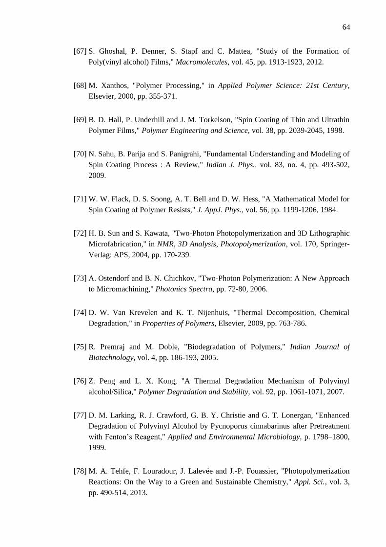
64
[67] S. Ghoshal, P. Denner, S. Stapf and C. Mattea, "Study of the Formation of
Poly(vinyl alcohol) Films," Macromolecules, vol. 45, pp. 1913-1923, 2012.
[68] M. Xanthos, "Polymer Processing," in Applied Polymer Science: 21st Century,
Elsevier, 2000, pp. 355-371.
[69] B. D. Hall, P. Underhill and J. M. Torkelson, "Spin Coating of Thin and Ultrathin
Polymer Films," Polymer Engineering and Science, vol. 38, pp. 2039-2045, 1998.
[70] N. Sahu, B. Parija and S. Panigrahi, "Fundamental Understanding and Modeling of
Spin Coating Process : A Review," Indian J. Phys., vol. 83, no. 4, pp. 493-502,
2009.
[71] W. W. Flack, D. S. Soong, A. T. Bell and D. W. Hess, "A Mathematical Model for
Spin Coating of Polymer Resists," J. AppJ. Phys., vol. 56, pp. 1199-1206, 1984.
[72] H. B. Sun and S. Kawata, "Two-Photon Photopolymerization and 3D Lithographic
Microfabrication," in NMR, 3D Analysis, Photopolymerization, vol. 170, Springer-
Verlag: APS, 2004, pp. 170-239.
[73] A. Ostendorf and B. N. Chichkov, "Two-Photon Polymerization: A New Approach
to Micromachining," Photonics Spectra, pp. 72-80, 2006.
[74] D. W. Van Krevelen and K. T. Nijenhuis, "Thermal Decomposition, Chemical
Degradation," in Properties of Polymers, Elsevier, 2009, pp. 763-786.
[75] R. Premraj and M. Doble, "Biodegradation of Polymers," Indian Journal of
Biotechnology, vol. 4, pp. 186-193, 2005.
[76] Z. Peng and L. X. Kong, "A Thermal Degradation Mechanism of Polyvinyl
alcohol/Silica," Polymer Degradation and Stability, vol. 92, pp. 1061-1071, 2007.
[77] D. M. Larking, R. J. Crawford, G. B. Y. Christie and G. T. Lonergan, "Enhanced
Degradation of Polyvinyl Alcohol by Pycnoporus cinnabarinus after Pretreatment
with Fenton’s Reagent," Applied and Environmental Microbiology, p. 1798–1800,
1999.
[78] M. A. Tehfe, F. Louradour, J. Lalevée and J.-P. Fouassier, "Photopolymerization
Reactions: On the Way to a Green and Sustainable Chemistry," Appl. Sci., vol. 3,
pp. 490-514, 2013.
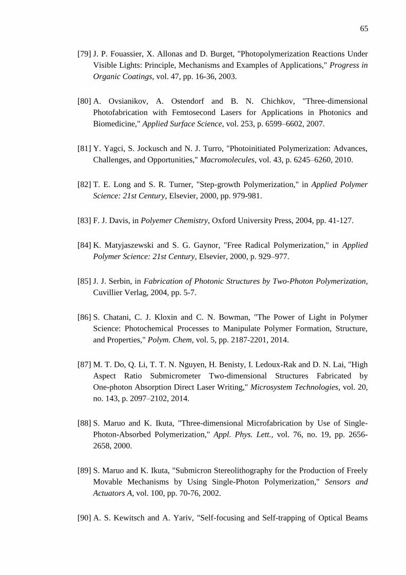
65
[79] J. P. Fouassier, X. Allonas and D. Burget, "Photopolymerization Reactions Under
Visible Lights: Principle, Mechanisms and Examples of Applications," Progress in
Organic Coatings, vol. 47, pp. 16-36, 2003.
[80] A. Ovsianikov, A. Ostendorf and B. N. Chichkov, "Three-dimensional
Photofabrication with Femtosecond Lasers for Applications in Photonics and
Biomedicine," Applied Surface Science, vol. 253, p. 6599–6602, 2007.
[81] Y. Yagci, S. Jockusch and N. J. Turro, "Photoinitiated Polymerization: Advances,
Challenges, and Opportunities," Macromolecules, vol. 43, p. 6245–6260, 2010.
[82] T. E. Long and S. R. Turner, "Step-growth Polymerization," in Applied Polymer
Science: 21st Century, Elsevier, 2000, pp. 979-981.
[83] F. J. Davis, in Polyemer Chemistry, Oxford University Press, 2004, pp. 41-127.
[84] K. Matyjaszewski and S. G. Gaynor, "Free Radical Polymerization," in Applied
Polymer Science: 21st Century, Elsevier, 2000, p. 929–977.
[85] J. J. Serbin, in Fabrication of Photonic Structures by Two-Photon Polymerization,
Cuvillier Verlag, 2004, pp. 5-7.
[86] S. Chatani, C. J. Kloxin and C. N. Bowman, "The Power of Light in Polymer
Science: Photochemical Processes to Manipulate Polymer Formation, Structure,
and Properties," Polym. Chem, vol. 5, pp. 2187-2201, 2014.
[87] M. T. Do, Q. Li, T. T. N. Nguyen, H. Benisty, I. Ledoux-Rak and D. N. Lai, "High
Aspect Ratio Submicrometer Two-dimensional Structures Fabricated by
One-photon Absorption Direct Laser Writing," Microsystem Technologies, vol. 20,
no. 143, p. 2097–2102, 2014.
[88] S. Maruo and K. Ikuta, "Three-dimensional Microfabrication by Use of Single-
Photon-Absorbed Polymerization," Appl. Phys. Lett., vol. 76, no. 19, pp. 2656-
2658, 2000.
[89] S. Maruo and K. Ikuta, "Submicron Stereolithography for the Production of Freely
Movable Mechanisms by Using Single-Photon Polymerization," Sensors and
Actuators A, vol. 100, pp. 70-76, 2002.
[90] A. S. Kewitsch and A. Yariv, "Self-focusing and Self-trapping of Optical Beams
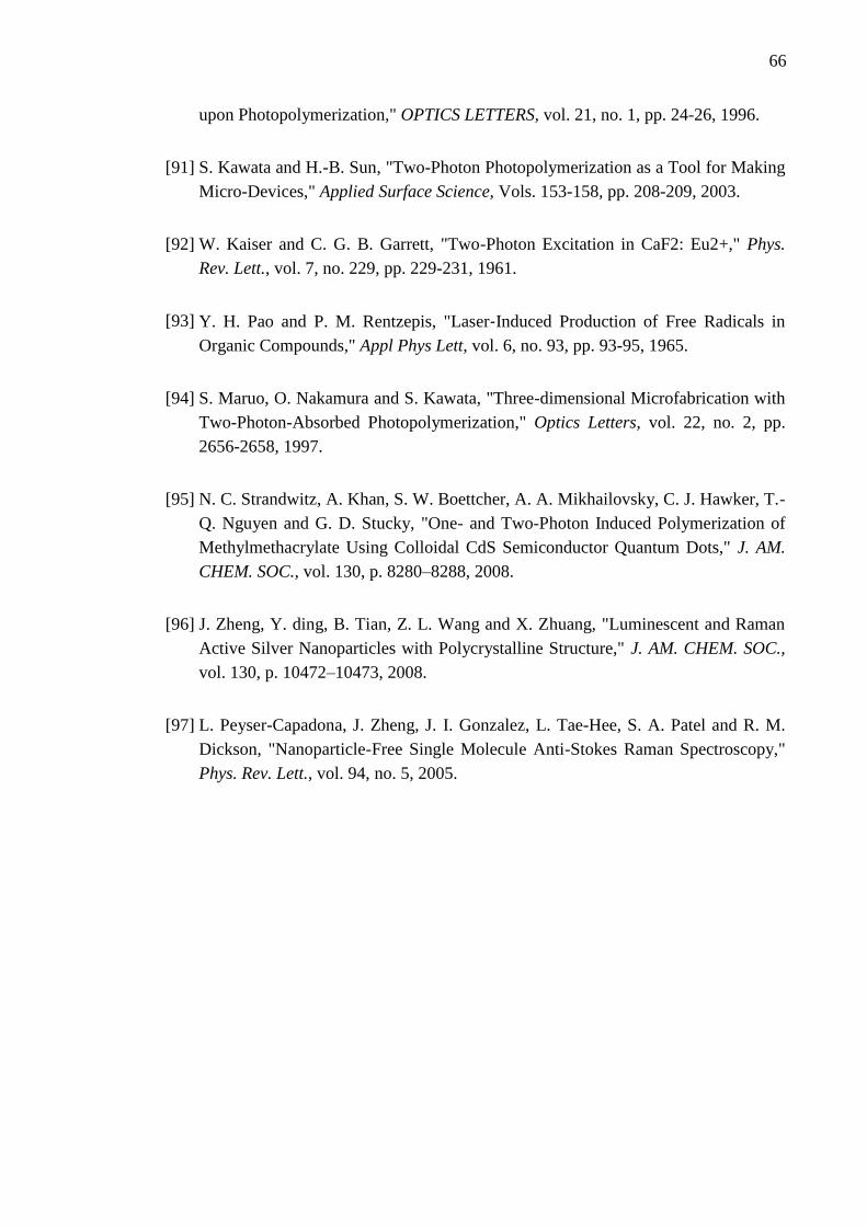
66
upon Photopolymerization," OPTICS LETTERS, vol. 21, no. 1, pp. 24-26, 1996.
[91] S. Kawata and H.-B. Sun, "Two-Photon Photopolymerization as a Tool for Making
Micro-Devices," Applied Surface Science, Vols. 153-158, pp. 208-209, 2003.
[92] W. Kaiser and C. G. B. Garrett, "Two-Photon Excitation in CaF2: Eu2+," Phys.
Rev. Lett., vol. 7, no. 229, pp. 229-231, 1961.
[93] Y. H. Pao and P. M. Rentzepis, "Laser‐Induced Production of Free Radicals in
Organic Compounds," Appl Phys Lett, vol. 6, no. 93, pp. 93-95, 1965.
[94] S. Maruo, O. Nakamura and S. Kawata, "Three-dimensional Microfabrication with
Two-Photon-Absorbed Photopolymerization," Optics Letters, vol. 22, no. 2, pp.
2656-2658, 1997.
[95] N. C. Strandwitz, A. Khan, S. W. Boettcher, A. A. Mikhailovsky, C. J. Hawker, T.-
Q. Nguyen and G. D. Stucky, "One- and Two-Photon Induced Polymerization of
Methylmethacrylate Using Colloidal CdS Semiconductor Quantum Dots," J. AM.
CHEM. SOC., vol. 130, p. 8280–8288, 2008.
[96] J. Zheng, Y. ding, B. Tian, Z. L. Wang and X. Zhuang, "Luminescent and Raman
Active Silver Nanoparticles with Polycrystalline Structure," J. AM. CHEM. SOC.,
vol. 130, p. 10472–10473, 2008.
[97] L. Peyser-Capadona, J. Zheng, J. I. Gonzalez, L. Tae-Hee, S. A. Patel and R. M.
Dickson, "Nanoparticle-Free Single Molecule Anti-Stokes Raman Spectroscopy,"
Phys. Rev. Lett., vol. 94, no. 5, 2005.