Embed Size (px)
Citation preview
M.Tech (Electronics-VLSI Design) Revised Syllabus Applicable w.e.f. Academic Session 2011-12
(22022012) Page 1 of 47
Study & Evaluation Scheme
Of
Master of Technology
(Electronics Engineering
- Specialization VLSI Design) [Applicable w.e.f. Academic Session 2011-12 till revised]
[with amendments in MHM 301 as approved on 20th
November 2012]
TEERTHANKER MAHAVEER UNIVERSITY N.H.-24, Delhi Road, Moradabad, Uttar Pradesh-244001
M.Tech (Electronics-VLSI Design) Revised Syllabus Applicable w.e.f. Academic Session 2011-12
(22022012) Page 2 of 47
Website:
www.tmu.ac.in
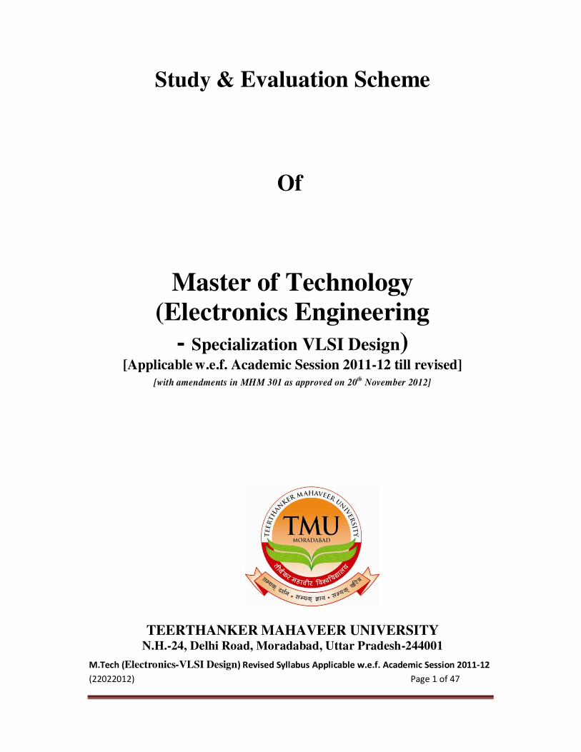
Study & Evaluation Scheme Of
Master of Technology-Electronics Engineering-
with specialization in VLSI Design SUMMARY
Programme : M.Tech (Electronics-VLSI Design)
Duration : Two years( Four semester)
Medium : English
Minimum Required Attendance : 75 %
Credits :
Maximum Credits : 80
Minimum credits required for : 76
degree
Assessment (Theory Papers) : Internal External Total
30 70 100
Internal Evaluation (Theory
Papers) :
1st Class
Test
2nd Class
Test
3rd Class
Test Assignment
(S)
Other
Activity Including
attendance
Total Best two of the three
class tests shall be considered
10
Marks
10
Marks
10
Marks
5 Marks 5 Marks 30
Marks
Evaluation of Practical /Thesis
: Internal External Total
50 50 100
Evaluation of Thesis
:
Internal External Total
Guide RC 50 100
25 25
Duration of Examination
:
External Internal
3 hrs. 1 ½ hrs
To qualify the course a student is required to secure a minimum of 40 % marks in aggregate including
the semester end examination and teachers continuous evaluation.(i.e. both internal and external).
A candidate who secures less than 40% marks in a course shall be deemed to have failed in that
course. In case a student has secured more than 40% marks in each course, but less than 50% in aggregate in a semester, he/she shall re-appear in courses where the marks are less than 50% to achieve
the required aggregate percentage of 50% in the semester. The student must secure the prescribed
minimum credits to be eligible for the award of degree. However he/she must have appeared in all papers.
TTEEEERRTTHHAANNKKEERR MMAAHHAAVVEEEERR UUNNIIVVEERRSSIITTYY ((EEssttaabblliisshheedd uunnddeerr GGoovvtt.. ooff UU.. PP.. AAcctt NNoo.. 3300,, 22000088)) DDeellhhii RRooaadd,, BBaaggaarrppuurr,, MMoorraaddaabbaadd ((UU..PP))
Question Paper Structure 1. The question paper shall consist of eight questions, out of which first question shall be of short answer type (not exceeding 50 words) and will be compulsory. Question No. 1 shall contain 8 parts representing all units of the
syllabus and students shall have to answer any five (weight age 4 marks each of them). 2. Out of the remaining seven questions, a student shall be required to attempt any five questions. There will be
minimum one and maximum two questions from each unit of the syllabus. The weight age of Question No. 2 to 8 shall be 10 marks each.
M.Tech (Electronics-VLSI Design) Revised Syllabus Applicable w.e.f. Academic Session 2011-12
(22022012) Page 3 of 47
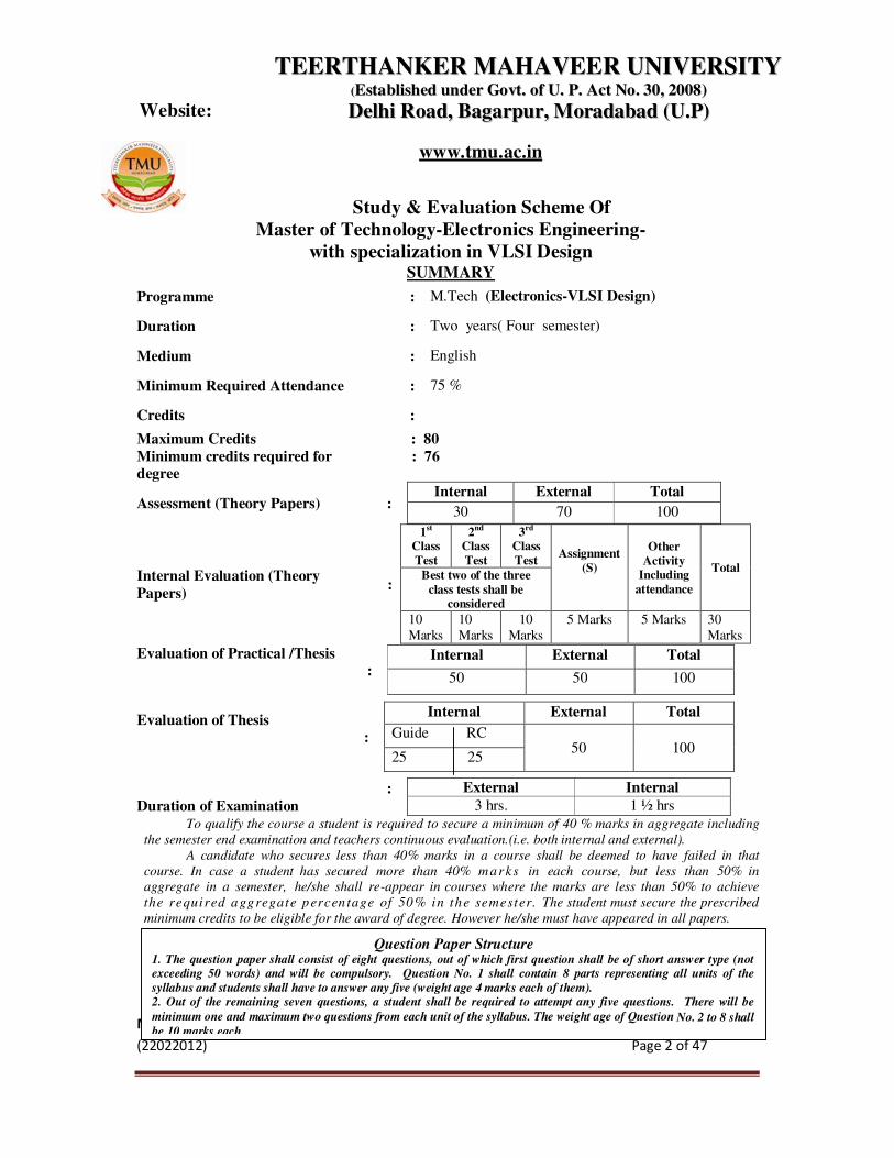
Study & Evaluation Scheme
Programme: M.Tech. (Electronics-VLSI Design)
Semester I
Semester II
S.
No
Course
Code
Subject Periods Credit Evaluation Scheme
L T P
Internal External Total
1 MEC101 MOS Circuit Design 3 2 - 4 30 70 100
2 MEC102 VLSI Technology 3 2 - 4 30 70 100
3 MEC103 Digital Systems
Design
3 2 - 4 30 70 100
4 MEC104 Digital Signal
Processing and
Applications
3 2 - 4 30 70 100
5 MEC151 EDA- (Lab) - - 4 2 50 50 100
Total 12 8 4 18 170 330 500
S.
No.
Course
Code
Subject Periods Credit Evaluation Scheme
L T P
Internal External Total
1 MEC201 Digital Systems Testing
and Simulation with VHDL
3 2 - 4 30 70 100
2 MEC203 Solid State Device Mode-
ling and Simulation
3 2 - 4 30 70 100
3 MEC233 Analog and low power digital
VLSI design 3 2 - 4 30 70 100
MEC234 Microcontroller and
Applications
4 MEC204 Nano-Technology
3 2 - 4 30 70 100
5 MEC
235
MEC
236
MEMS and
IC Integration
Compound
Semiconduc
tor Material
and Devices
3
2
-
4
30 70
100
6 MEC251 HDL- (Lab) - - 4 2 50 50 100
7 MEC291 Seminar - - 4 2 50 50 100
Total 15 10 8 24 250 450 700
M.Tech (Electronics-VLSI Design) Revised Syllabus Applicable w.e.f. Academic Session 2011-12
(22022012) Page 4 of 47
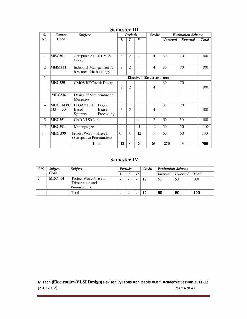
Semester III S.
No.
Course
Code
Subject Periods Credit Evaluation Scheme
L T P Internal External Total
1 MEC301 Computer Aids for VLSI
Design
3 2 - 4 30 70 100
2 MHM301 Industrial Management &
Research Methodology
3 2 - 4 30 70 100
3 Elective I (Select any one)
MEC335 CMOS RF Circuit Design
3
2
-
4
30 70
100
MEC336 Design of Semiconductor
Memories
4 MEC 333
MEC334
FPGA/CPLD Based
Systems
Digital Image
Processing
3
2
-
4
30 70 100
5 MEC351 CAD VLSI(Lab) - - 4 2 50 50 100
6 MEC391 Minor project - - 4 2 50 50 100
7 MEC 399 Project Work – Phase I (Synopsis & Presentation)
0 0 12 6 50 50 100
Total 12 8 20 26 270 430 700
Semester IV
S.N. Subject
Code
Subject Periods Credit Evaluation Scheme
L T P Internal External Total
1 MEC 401 Project Work-Phase II
(Dissertation and
Presentation)
- - - 12 50 50 100
Total - - - 12 50 50 100
M.Tech (Electronics-VLSI Design) Revised Syllabus Applicable w.e.f. Academic Session 2011-12
(22022012) Page 5 of 47
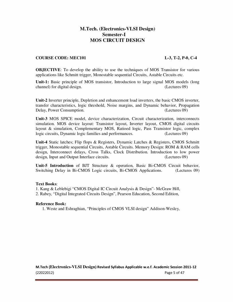
M.Tech. (Electronics-VLSI Design)
Semester-I
MOS CIRCUIT DESIGN
COURSE CODE: MEC101 L-3, T-2, P-0, C-4
OBJECTIVE: To develop the ability to use the techniques of MOS Transistor for various
applications like Schmitt trigger, Monostable sequential Circuits, Astable Circuits etc.
Unit-1: Basic principle of MOS transistor, Introduction to large signal MOS models (long
channel) for digital design. (Lectures 09)
Unit-2 Inverter principle, Depletion and enhancement load inverters, the basic CMOS inverter,
transfer characteristics, logic threshold, Noise margins, and Dynamic behavior, Propagation Delay, Power Consumption. (Lectures 09)
Unit-3 MOS SPICE model, device characterization, Circuit characterization, interconnects
simulation. MOS device layout: Transistor layout, Inverter layout, CMOS digital circuits layout & simulation, Complementary MOS, Ratioed logic, Pass Transistor logic, complex
logic circuits, Dynamic logic families and performances. (Lectures 09)
Unit-4 Static latches; Flip flops & Registers, Dynamic Latches & Registers, CMOS Schmitt
trigger, Monostable sequential Circuits, Astable Circuits. Memory Design: ROM & RAM cells
design, Interconnect delays, Cross Talks, Clock Distribution. Introduction to low power
design, Input and Output Interface circuits. (Lectures 09)
Unit-5 Introduction of BJT Structure & operation, Basic Bi-CMOS Circuit behavior, Switching Delay in Bi-CMOS Logic circuits, Bi-CMOS Applications. (Lectures 09)
Text Books: 1. Kang & Leblebigi “CMOS Digital IC Circuit Analysis & Design”- McGraw Hill,
2. Rabey, “Digital Integrated Circuits Design”, Pearson Education, Second Edition,
Reference Book:
1. Weste and Eshraghian, “Principles of CMOS VLSI design” Addison-Wesley,
M.Tech (Electronics-VLSI Design) Revised Syllabus Applicable w.e.f. Academic Session 2011-12
(22022012) Page 6 of 47
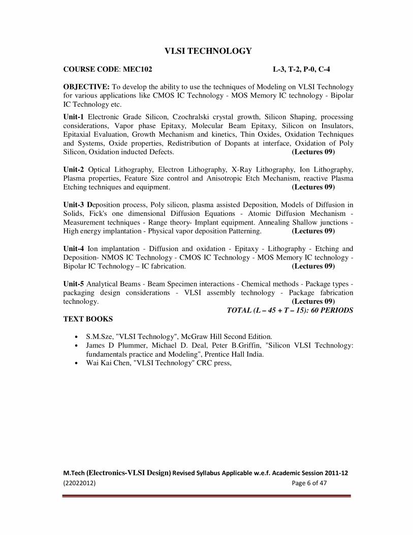
VLSI TECHNOLOGY
COURSE CODE: MEC102 L-3, T-2, P-0, C-4
OBJECTIVE: To develop the ability to use the techniques of Modeling on VLSI Technology for various applications like CMOS IC Technology - MOS Memory IC technology - Bipolar
IC Technology etc.
Unit-1 Electronic Grade Silicon, Czochralski crystal growth, Silicon Shaping, processing
considerations, Vapor phase Epitaxy, Molecular Beam Epitaxy, Silicon on Insulators, Epitaxial Evaluation, Growth Mechanism and kinetics, Thin Oxides, Oxidation Techniques
and Systems, Oxide properties, Redistribution of Dopants at interface, Oxidation of Poly Silicon, Oxidation inducted Defects. (Lectures 09)
Unit-2 Optical Lithography, Electron Lithography, X-Ray Lithography, Ion Lithography,
Plasma properties, Feature Size control and Anisotropic Etch Mechanism, reactive Plasma
Etching techniques and equipment. (Lectures 09)
Unit-3 Deposition process, Poly silicon, plasma assisted Deposition, Models of Diffusion in
Solids, Fick's one dimensional Diffusion Equations - Atomic Diffusion Mechanism -
Measurement techniques - Range theory- Implant equipment. Annealing Shallow junctions - High energy implantation - Physical vapor deposition Patterning. (Lectures 09)
Unit-4 Ion implantation - Diffusion and oxidation - Epitaxy - Lithography - Etching and
Deposition- NMOS IC Technology - CMOS IC Technology - MOS Memory IC technology -
Bipolar IC Technology – IC fabrication. (Lectures 09)
Unit-5 Analytical Beams - Beam Specimen interactions - Chemical methods - Package types -
packaging design considerations - VLSI assembly technology - Package fabrication
technology. (Lectures 09)
TOTAL (L – 45 + T – 15): 60 PERIODS
TEXT BOOKS
• S.M.Sze, "VLSI Technology", McGraw Hill Second Edition.
• James D Plummer, Michael D. Deal, Peter B.Griffin, "Silicon VLSI Technology:
fundamentals practice and Modeling", Prentice Hall India. • Wai Kai Chen, "VLSI Technology" CRC press,
M.Tech (Electronics-VLSI Design) Revised Syllabus Applicable w.e.f. Academic Session 2011-12
(22022012) Page 7 of 47
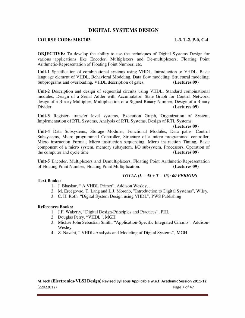
DIGITAL SYSTEMS DESIGN
COURSE CODE: MEC103 L-3, T-2, P-0, C-4
OBJECTIVE: To develop the ability to use the techniques of Digital Systems Design for
various applications like Encoder, Multiplexers and De-multiplexers, Floating Point Arithmetic-Representation of Floating Point Number, etc.
Unit-1 Specification of combinational systems using VHDL, Introduction to VHDL, Basic
language element of VHDL, Behavioral Modeling, Data flow modeling, Structural modeling,
Subprograms and overloading, VHDL description of gates. (Lectures 09)
Unit-2 Description and design of sequential circuits using VHDL, Standard combinational
modules, Design of a Serial Adder with Accumulator, State Graph for Control Network,
design of a Binary Multiplier, Multiplication of a Signed Binary Number, Design of a Binary
Divider. (Lectures 09)
Unit-3 Register- transfer level systems, Execution Graph, Organization of System,
Implementation of RTL Systems, Analysis of RTL Systems, Design of RTL Systems.
(Lectures 09)
Unit-4 Data Subsystems, Storage Modules, Functional Modules, Data paths, Control
Subsystems, Micro programmed Controller, Structure of a micro programmed controller, Micro instruction Format, Micro instruction sequencing, Micro instruction Timing, Basic
component of a micro system, memory subsystem. I/O subsystem, Processors, Operation of the computer and cycle time (Lectures 09)
Unit-5 Encoder, Multiplexers and Demultiplexers, Floating Point Arithmetic-Representation
of Floating Point Number, Floating Point Multiplication. (Lectures 09)
TOTAL (L – 45 + T – 15): 60 PERIODS Text Books:
1. J. Bhaskar, “ A VHDL Primer”, Addison Wesley, .
2. M. Ercegovac, T. Lang and L.J. Moreno, ”Introduction to Digital Systems”, Wiley,
3. C. H. Roth, “Digital System Design using VHDL”, PWS Publishing
References Books:
1. J.F. Wakerly, “Digital Design-Principles and Practices”, PHL
2. Douglas Perry, “VHDL”, MGH
3. Michae John Sebastian Smith, “Application-Specific Integrated Circuits”, Addison-
Wesley.
4. Z. Navabi, “ VHDL-Analysis and Modeling of Digital Systems”, MGH
M.Tech (Electronics-VLSI Design) Revised Syllabus Applicable w.e.f. Academic Session 2011-12
(22022012) Page 8 of 47
DIGITAL SIGNAL PROCESSING AND APPLICATIONS
COURSE CODE: MEC104 L-3, T-2, P-0, C-4
OBJECTIVE: To develop the ability to use the techniques of Digital Signal Processing for various applications like real time system, Sampling of low pass & band pass signals Digital
audio Mixing, Speech synthesis and recognition etc.
Unit-1 Representation of signals on orthogonal basis; Sampling and Reconstruction of signals;
Z-Transform, Analysis of LSI systems, Frequency analysis, Inverse systems, Discrete Fourier Transform (DFT), Fast Fourier Transform algorithm, Implementation of Discrete time
systems. (Lectures 09)
Unit-2 Design of FIR Digital filters: Window method, Park-McClellan’s method.
(Lectures 09)
Unit-3 Butterworth Chebyshev and Elliptic Approximations low pass, Band pass, Band stop and High pass filters. Effect of finite register length in FIR filter design Parametric and non-
parametric spectra estimation. Introduction to multirate signal processing. (Lectures 09)
Unit-4 Block diagram of real time system, Sampling of low pass & band pass signals, Uniform
& non-uniform quantization and encoding , over sampling in A/D conversion, D/A conversion process, Anti imaging filtering, over sampling in D/ A conversion, limitations of real time
signal processing with analog input/output signals application (Lectures 09)
Unit-5 Applications of MultiMate Signal Processing: Design of Phase Shifters, Sub band Coding of Speech Signals, Digital Filter Banks, Two Channel Quadrature Mirror Filter Banks,
Channel QMF Bank. (Lectures 09)
TOTAL (L – 45 + T – 15): 60 PERIODS
Text Books:
1. Discrete Time signal Processing, A.V. Oppenheim and Schafer, Prentice Hall, 2. Digital Signal Processing : Principle, Algorithms and Applications, John G. Proakis
and D.G. Manolakis, Prentice Hall, 3. Theory and Application of Digital Signal Processing: L.R. Rabiner and B. Gold,
Prentice Hall,
Reference Books 1. Introduction to Digital Signal Processing: J.R. Johnson, Prentice Hall,
2. Digital Signal Processing: D. J. DeFatta, J. G. Lucas and W. S. Hodgkiss, J Wile
and sons, Singapore.
M.Tech (Electronics-VLSI Design) Revised Syllabus Applicable w.e.f. Academic Session 2011-12
(22022012) Page 9 of 47
EDA- (Lab)
L-0, T-0, P-4, C-2
COURSE CODE: MEC151
List of Experiments
1) Signal generation by using DSP tools.
2) To check the properties of LTI systems.
3) Find the Linear convolution, circular convolution.
4) Find the DFT by using convolution.
5) Find the FFT by using radix-2.
6) Design FIR filter.
7) Design IIR filter.
8) Applications of multirate signal processing.
9) Application of MAT lab in Digital Communication.
M.Tech (Electronics-VLSI Design) Revised Syllabus Applicable w.e.f. Academic Session 2011-12
(22022012) Page 10 of 47
DIGITAL SYSTEMS TESTING AND SIMULATION WITH VHDL
COURSE CODE: MEC201 L-3, T-2, P-0, C-4
OBJECTIVE: To develop the ability to use the techniques of testing for various models, applications like logic model, fault model, Fault Simulation, Deductive fault simulation etc.
Unit-1 Testing definitions and areas within testing. Logic and Fault Modeling. Mechanics
Definitions: Abstractions level, Faults and errors, Modeling, Test Evaluation,
Test Generation, Diagnostics. System life, Sources of defects. (Lectures 09)
Unit-2 Representation and models of digital systems across abstraction levels. Fault Models: logical versus physical; SSF model, opens and shorts, bridging
faults; Basic assumptions. (Lectures 09)
Unit-3 Review of minimization tools and asynchronous machines, Test Pattern Generation basics. (activate and drive.), Algebraic approaches, Fault Equivalence and Dominance.
(Lectures 09)
Unit-4 Algebraic Approaches and Structural Approaches, Logic Simulation. Algebraic
Approaches: Boolean difference, Literal position, Effect of fan-out on circuits, Checkpoint
faults. Structural Approaches to test generation. Path sensitization methods.
(Lectures 09)
Unit-5 Compiler, event driven. Representation of value, circuit, etc. Logic and Fault.
Simulation: Delay models for circuit simulation, Fault Simulation Purpose of Serial and
Parallel Fault Simulation, Deductive fault simulation. Concurrent Fault Simulation, Critical
Path tracing, Statistical Fault Analysis. (Lectures 09)
TOTAL (L – 45 + T – 15): 60 PERIODS
Text Books: 1. "Digital Systems Testing and Testable Design" by Miron Abramovici, Melvin Breuer
and Arthur Friedman, IEEE press, NY. 2. A Guide to VHDL'' by Stanley Mazor, Kluwer Academic Press
Reference Books:
1. "HDL Chip Design" by Douglas Smith, Doone Publications, AL.
2. "Rapid Prototyping of Digital Systems", by J. O. Hamblen and M. Furman, Kluwer
Academic Publishers.
M.Tech (Electronics-VLSI Design) Revised Syllabus Applicable w.e.f. Academic Session 2011-12
(22022012) Page 11 of 47
SOLID STATE DEVICE MODELING AND SIMULATION
COURSE CODE: MEC203 L-3, T-2, P-0, C-4
OBJECTIVE: To develop the ability to use the techniques of
Solid State Device Modeling and Simulation for various applications like Depletion
Capacitance, Series Resistances, Early Effect, Gummel Plots etc.
Unit-1 Quantum Mechanical Concepts, Carrier Concentration, Transport Equation, Band gap,
Mobility and Resistivity, Carrier Generation and Recombination, Avalanche Process, Noise
Sources. (Lectures 09)
Unit-2 Injection and Transport Model, Continuity Equation, Diode Small Signal and Large
Signal (Change Control Model), Transistor Models: Eber’s - Moll and Gummel Port Model,
SPICE modeling temperature and area effects. (Lectures 09)
Unit-3 Introduction Interior Layer, MOS Transistor Current, Threshold Voltage, Temperature
Short Channel and Narrow Width Effect, Models for Enhancement, Depletion Type MOSFET,
CMOS Models in SPICE. (Lectures 09)
Unit-4 General Methods, Specific Bipolar Measurement, Depletion Capacitance, Series
Resistances, Early Effect, Gummel Plots, MOSFET: Long and Short Channel Parameters,
Statistical Modeling of Bipolar and MOS Transistor. (Lectures 09)
Unit-5 Static and Dynamic Models, Rate Equations, Numerical Technique, Equivalent
Circuits, Modeling of LEDs, Laser Diode and Photo-detectors. (Lectures 09)
TOTAL (L – 45 + T – 15): 60 PERIODS
Text Books: 1. Philip E. Allen, Douglas R. Hoberg, "CMOS Analog Circuit Design", Second
Edition, Oxford Press 2. S.M.Sze "Semiconductor Devices - Physics and Technology", John Wiley and
sons.
References Books:
1. Kiat Seng Yeo, Samir S.Rofail, Wang-Ling Gob, "CMOS / BiCMOS ULSI - Low
Voltage, low Power", Person education, Low price edition.
M.Tech (Electronics-VLSI Design) Revised Syllabus Applicable w.e.f. Academic Session 2011-12
(22022012) Page 12 of 47
ANALOG AND LOW POWER DIGITAL VLSI DESIGN (ELECTIVE)
COURSE CODE: MEC233 L-3, T-2, P-0, C-4
OBJECTIVE: To develop the ability to use the techniques of low power for various
applications like Low power Static RAM architecture, Software design for low power, Case
studies of Gilbert Cell Design with layout for low power.
Unit 1 Low Power Design and Physics of Power Consumption, Power Estimation and
Synthesis for low power, Design and test of low voltage CMOS circuits. (Lectures 09)
Unit 2 Low power Static RAM architecture, Low power computing with energy recovery,
Digital low power design using hazard filters and balanced parities (Lectures 09)
Unit 3 Software design for low power, Case studies of Gilbert Cell Design with layout for low power. (Lectures 09)
Unit 4 Case study of PLL design with layout for low power, Case study of A/D and D/A
Converters for low power applications. (Lectures 09)
Unit 5 Low power design for wireless circuits, Integrated radio frequency CMOS design.
(Lectures 09)
TOTAL (L – 45 + T – 15): 60 PERIODS
Text Books: 1. Introduction to Low-Power VLSI Design (G Yeap & A Wild)
2. Low Power Design of Off-Chip Drivers and Transmission Lines: A Branch and
Bound Approach (R Gupta et al.)
Reference Books: 3. A New CMOS Driver Model for Transient Analysis and Power Dissipation
Analysis (H Liao et al.)
4. On the Optimal Drivers of High-Speed Low Power ICs (D Zhou & X Y Liu)
5. Floorplan Design with Low Power Considerations (K-Y Chao & D F Wong)
M.Tech (Electronics-VLSI Design) Revised Syllabus Applicable w.e.f. Academic Session 2011-12
(22022012) Page 13 of 47
MICROCONTROLLER AND APPLICATIONS (ELECTIVE)
COURSE CODE: MEC234 L-3, T-2, P-0, C-4
OBJECTIVE: To develop the ability to use the techniques of synchronization in data transfer and handshaking, interrupt management, interrupt service routines, Design with
Microcontrollers.
Unit-1 Single Chip Controllers, Design and testing of software for Micro-controllers,
Architectural features of different types of architectures used in Micro-controllers, like Van
Neuman, Harward, CISC, RISC, SISC architectures. Special features like watchdog timer,
digital signal processors, clock monitor, resident program, loader, monitor, General
applications of Micro-controllers. (Lectures 09)
Unit-2 Comparison of Intel MCS 51/251 and MCS 96 Microcontroller Families, Overview
and features of MCS 96(HSIO) family, Intel 80C196 CHMOS 16 bit Microcontroller, Pin
configuration, Architectural block diagram, Signal descriptions, memory and address space,
registers, buses, and data transfers, different modes of operation. (Lectures 09)
Unit-3 Instruction set : different types of instructions, instruction significance and execution,
Addressing modes, effective address, simple programs, loop programs, subroutines and
examples, Memory Management, Programming the Microcontroller for different applications,
Synchronous Serial Port, Serial port wave forms (shift register mode), Interrupts handling and
priority, External Memory Interfacing. (Lectures 09)
Unit-4 Serial and parallel ports and software control of ports, port I/O registers,
synchronization in data transfer and handshaking, interrupt management, interrupt service
routines, and interrupt examples keeping time and parallel port transfers, A/D control and status registers and applications. (Lectures 09)
Unit-5 Interfacing of LEDs, Switches and 7- segment displays, keyboard interfacing, RS-232
interfacing, DC motor interfacing, Stepper motor interfacing, DAC, Data acquisition system, real world interfacing. (Lectures 09)
TOTAL (L – 45 + T – 15): 60 PERIODS
Text Books:
1. The 8051 Microcontroller, 3rd Ed., Scott MacKenzie,, Prentice Hall.
2. The 80251 Microcontroller, Kenneth Ayala, Prentice Hall.
3. The 8051 Microcontroller: Hardware, Software, and Interfacing, 2nd Ed, James Stewart and
Kai Miao, Prentice Hall.
Reference Books:
1. The art of programming embedded systems by Jack G. Ganssle.
2. Design with Microcontrollers by John B. Peatman.
M.Tech (Electronics-VLSI Design) Revised Syllabus Applicable w.e.f. Academic Session 2011-12
(22022012) Page 14 of 47
NANO-TECHNOLOGY Course Code: MEC 204 L T P C
3 2 0 4
Objective: The purpose of this course is to convey the conceptual framework that underlies
this microscopic viewpoint using examples related to the emerging field of Nano Technology.
Unit-1
Introduction: Introduction to Nanotechnology: Characteristic scale for quantum phenomena,
nanoparticles, nano-clusters, nanotubes, nanowires and nanodots. Drexler-Smalley debate - realistic projections. (Lectures 09)
Unit-2
Technology of Nano-materials deposition-I-: Lithography; Nano-Lithography; Nano-Imprint Lithography; Photo Lithography; E-Beam Lithography; X-Ray- Lithography; Iron Beam
Lithography; Scanning Probe Lithography; Dip-Pen Lithography. (Lectures 09)
Unit-3 Technology of Nano-materials deposition-II-: Top-Down& Bottom-Up Approach; Ball
Milling; Sputtering; CVD, PVD; Sol-Gel Technique; Laser Ablation Technique; Molecular
Beam-Epitaxi Technique. (Lectures 09)
Unit-4 Microscopic & Spectroscopic Techniques – Optical ; Fluorescence Con-focal; SEM; TEM;
STEM; STM; AFM-contact & non-contact mode ; MRI; XRD; Scanning probe Microscope.
(Lectures 09)
Unit-5 Carbon Nano-materials – Fullerene (Bucky Balls); Carbon Nano-tubes- Types, Preparation
& Potential Applications and emerging techniques (Lectures 09)
TOTAL (L – 45 + T – 15): 60 PERIODS
Text Books:
1. “A Text Book of NanoScience”Dhanpat Rai & Co. (P) Ltd.-Dr. Sunita Singh 2. “Introduction To Solid State Physics” by John Wiley Interscience, Ed 8-Charles
Kitte 3. “Nanoelectronics: Nanowires, Molecular Devices,”Tata McGraw Hill,-Krzysztof
Iniewski 4. “Nanoelectronics & Information,”Wiley-VCH, Berlin
M.Tech (Electronics-VLSI Design) Revised Syllabus Applicable w.e.f. Academic Session 2011-12
(22022012) Page 15 of 47
MEMS AND IC INTEGRATION
COURSE CODE: MEC 235 L-3, T-2, P-0, C-4
OBJECTIVE: To develop the ability to use the techniques of Pressure sensors with embedded
electronics IC fabrication, MEMS system-level design methodology for various applications
like et.
Unit-1 Introduction, emergence, devices and application, scaling issues, materials for MEMS,
Thin film deposition, lithography and etching. (Lectures 09)
Unit-2 Bulk micro machining: Introduction, etch-stop techniques, dry etching, buried oxide process, silicon fusion bonding, and anodic bonding. (Lectures 09)
Unit-3 Surface micro machining: Introduction, sacrificial layer technology, material systems
in sacrificial layer technology, plasma etching, combined IC technology and anisotropic wet etching. (Lectures 09)
Unit-4 Microstereolithography: Introduction, Scanning Method, Projection Method, Applications. LIGA Process: Introduction, Basic Process and Application (Lectures 09)
Unit-5 MEMS devices, electronic interfaces, design, simulation and layout of MEMS devices
using CAD tools. (Lectures 09)
TOTAL (L – 45 + T – 15): 60 PERIODS
TEXT BOOKS: 1. S.M. Sze, Semiconductor Sensors, John Wiley & Sons, INC.
2. M.Elwenspoek, R.Wiegerink, Mechanical Microsensors, Springer-Verlag Berlin
Heidelberg.
REFERENCE BOOKS:
1. Massood Tabib-Azar, Microactuators - Electrical, Magnetic, Thermal, Optical, Mechanical, Chemical and Smart structures, Kluwer Academic Publishers, New
York. 2. Eric Udd , Fiber Optic Smart Structures , John Wiley & Sons, New York.
M.Tech (Electronics-VLSI Design) Revised Syllabus Applicable w.e.f. Academic Session 2011-12
(22022012) Page 16 of 47
COMPOUND SEMICONDUCTOR MATERIAL AND DEVICES
COURSE CODE: MEC 236 L-3, T-2, P-0, C-4
OBJECTIVE: To develop the ability to use the techniques of Liquid Phase Epitaxy,
Molecular Beam Epitaxy, HBT, DHBT, Heterostructure laser, waveguides and optical
modulators and switches etc.
Unit-1 III-V and II-VI compound semiconductor materials and their applications in electronics
and optoelectronic devices, crystal structures and their band structures, variation of band gap
with the contents of compound metals, refractive index variation with respect to the contents
of compound metals. (Lectures 09)
Unit-2 Liquid Phase Epitaxy, Molecular Beam Epitaxy, and Metal Organic Chemical Vapor
Deposition techniques for crystal growth. (Lectures 09)
Unit-3 HBT, DHBT, Heterostructure laser, waveguides and optical modulators and switches,
SLAPDS, and other Heterostructure p-i-n diodes. (Lectures 09)
Unit-4 Photoluminescence Techniques, X-Ray diffraction, SIMS, SEM, TEM, measurement of waveguides, modulator and optical detector. (Lectures 09)
Unit-5 Introduction to organic optoelectronics, Structure and physics of organic light emitting
diodes (OLEDs) Figures of merit for OLEDs. (Lectures 09)
TOTAL (L – 45 + T – 15): 60 PERIODS
Text Books:
1. Stephen A. Campell. “The science and engineering of microelectronics fabrication”, Oxford
University Press. .
2. Donald L. Smith. “Thin Film Deposition”. McGraw Hill. 1995.
3. Physics of Semiconductor Devices”, S.Sze, 2 Edition, Wiley
Reference Books: 1. H. C. Cassey and M. B. Panish. “Heterostructure Laser”. Academic Press
2. M. J. Kelly. “Low Dimensional Semiconductor Materials, Physics Technology,
Devices”. Oxford Science Publication. 1995. 3.John L. Vossen and Werner Kern. “Thin Film Processes II”. Academic Press Inc.
M.Tech (Electronics-VLSI Design) Revised Syllabus Applicable w.e.f. Academic Session 2011-12
(22022012) Page 17 of 47
HDL- (Lab)
L-0, T-0, P-4, C-2
COURSE CODE: MEC251
List of Experiments
1. Exposure to high-level design tools including high-level and logic synthesis
2. Design and simulation of half adder and full adder.
3. Design and simulation of various multiplexer and D-Mux
4. Design and simulation of various flip flops
5 Design and simulation of 8 bit and 16 bit register
6. Design and simulation of Encoder
7. Design and simulation of ALU and its realization on Xilinx FPGA
8. Synthesis of half adder and full adder circuit
M.Tech (Electronics-VLSI Design) Revised Syllabus Applicable w.e.f. Academic Session 2011-12
(22022012) Page 18 of 47
SEMINAR
COURSE CODE: MEC291 L-0, T-0, P-4, C-2
Selection of topic:
1. All students pursuing M.Tech shall submit the proposed topic of the seminar (from the
related field) in the first week of the semester to the course coordinator. Care should be taken that the topic selected does not directly relate to the subject of the courses being
pursued or seminar work, if any. The course coordinator shall then forward the list to the concerned department coordinators who will vet the list and add some more topics in
consultation with the faculty of the department .The topics will then be allocated to the students along with the name of the faculty guide and list will be put -up to the director for
approval.
2. On approval by the Director, the list shall be displayed on the notice boards and students
will be informed by the course coordinator. The intimation to the students of their seminar
subjects shall be within three weeks of the commencement of the semester.
Preparation of the seminar
1. The student shall meet the guide for the necessary guidance for the thesis work.
2. During the next two to four weeks the student should read the primary literature germane
to the seminar topic. Reading selection should continuously be informed to the guide.
3. After necessary collection of data and literature survey, the students must prepare a
report. The report shall be arranged in the sequence consisting of the following:-
a. Top Sheet of transparent plastic.
b. Top cover.
c. Preliminary pages.
(i) Title page
(ii) Certification page.
(iii) Acknowledgment.
(iv) Abstract.
(v) Table of Content.
(vi) List of Figures and Tables.
(vii) Nomenclature.
d. Chapters (Main Material).
e. Appendices, If any.
f. Bibliography/ References.
g. Evaluation Form.
h. Back Cover (Blank sheet).
i. Back Sheet of Plastic (May be opaque or transparent).
4. Top Cover- The sampled top cover shall be as Under:
M.Tech (Electronics-VLSI Design) Revised Syllabus Applicable w.e.f. Academic Session 2011-12
(22022012) Page 19 of 47
TITLE OF THE SEMINAR
NAME OF THE STUDENT WITH COURSE, STREAM, SEMESTER & SECTION.
Department of Electronics and Communication Engineering
College of Engineering
Teerthanker Mahaveer University
Moradabad-244001
MONTH AND YEAR
5. Title Page:- The Title Page cover shall be as Under:
Title of the seminar
M.Tech. seminar
(Submitted in Partial fulfillment of the requirement for the degree of
MASTER OF TECHNOLOGY
In
ELECTRONICS & COMMUNICATION ENGINEERING
(Specialization in VLSI)
by
Name of Student in capital Letters
(Roll No.)
COLLEGE OF ENGINEERING
TEERTHANKER MAHAVEER UNIVERSITY
N.H. 24, BAGARPUR,
MORADABAD-244001
MONTH AND YEAR
Name of the college and University.
Month and Year
6. Certification page:- This shall be as under
M.Tech (Electronics-VLSI Design) Revised Syllabus Applicable w.e.f. Academic Session 2011-12
(22022012) Page 20 of 47
Department of Electronics and Communication Engineering
College of Engineering
Teerthankar Mahaveer University
Moradabad-244001
T
he seminar Report and Title “Name of the Topic of the seminar.”
Submitted by Mr. /Ms. (Name of the student) (Roll No.) may be accepted for being evaluated
Date Signature
Place (Name of guide)
For Guide If you Choose not to sign the acceptance certificate above, please indicate reasons
for the same from amongst those given below:
i) The amount of time and effort put in by the student is not sufficient;
ii) The amount of work put in by the student is not adequate;
iii) The report does not represent the actual work that was done / expected to be done;
iv) Any other objection (Please elaborate)
7. Abstract:- A portion of the seminar grade will be based on the abstract. The abstract will
be graded according to the adherence to accepted principles of English grammar and
according to the adherence to the format described below.
The seminar abstract is an important record of the coverage of your topic and provides a
valuable source of leading references for students and faculty alike. Accordingly, the abstract must serve as an introduction to your thesis topic. It will include the key
hypotheses, the major scientific findings and a brief conclusion. The abstract will be
limited to 500 words, excluding figures, tables and references. The abstract will
include references to the research articles upon which the thesis is based as well as research articles that have served as key background material.
M.Tech (Electronics-VLSI Design) Revised Syllabus Applicable w.e.f. Academic Session 2011-12
(22022012) Page 21 of 47
8. Table of Content:- This shall be as under:
APPENDIX IV: SAMPLE SHEET FOR TABLE OF CONTENTS
TABLE OF CONTENTS
Chapter No Title Page No.
Certificate Ii
Abstract Iii
Acknowledgement Iv
List of Figures V
List of Table Vi
1 Introduction 1
1.1
1.2
1.3
2 …………………..
3 ……………….....
4 References/ Bibliography
5 Evaluation sheet ……..
9. List of Figures and Tables:- This will be as under
List of Figures and Tables - sample entries are given below:
List of Figures
Figure
No.
Caption / Title
Page
No.
2.1 Schematic representation of a double layered droplet . . . 21
. . .
3.2 Variation in rate versus concentration . . . 32
M.Tech (Electronics-VLSI Design) Revised Syllabus Applicable w.e.f. Academic Session 2011-12
(22022012) Page 22 of 47
List of Tables - sample entries are given below:
List of Tables
Table
No.
Caption / Title
Page
No.
2.1 Thickness of a double layered droplet . . . 22
. . .
3.2 Variation in rate versus concentration . . . 34
12. Main Pages:-
The Main report should be divided in chapters ( 1,2,3 …..etc) and structured into sections (1.1, 1.2 ……..etc) and subsection (1.2.1, 1.2.2, ….. etc). Suitable title
should be given for section and subsection where necessary.
Referencing style- wherever reference is given in the main pages it should have the
following format.
The values of thermal conductivities for a variety of substances have been reported by Varma
(1982). For polymers, however, the information is more limited and some recent reviews have
attempted to fill the gaps (Batchelor and Shah, 1985).
For two authors -
(Batchelor and Kapur, 1985)
For more than two authors -
(Batchelor et al., 1986)
By same author/combination of authors in the same year -
(Batchelor, 1978a; Batchelor, 1978b; Batchelor et al., 1978)
13. Bibliography/References-
In the bibliography/ references list standard formats must
be used. The typical formats are given blow-
M.Tech (Electronics-VLSI Design) Revised Syllabus Applicable w.e.f. Academic Session 2011-12
(22022012) Page 23 of 47
Journal articles: -
David, A.B., Pandit, M.M. and Sinha, B.K., 1991, "Measurement of
surface viscosity by tensiometric methods", Chem. Engng Sci.47,
931-945.
Books: -
Doraiswamy, L.K. and Sharma, M.M., 1984, "Heterogeneous Reactions- Vol 1", Wiley, New York, pp 89-90.
Edited books/Compilations/Handbooks: -
Patel, A.B., 1989, "Liquid -liquid dispersions", in Dispersed Systems Handbook, Hardy, L.C. and Jameson, P.B. (Eds.), McGraw Hill,
Tokyo, pp 165-178.
Lynch, A.B. (Ed.), 1972, "Technical Writing", Prentice Hall, London.
Theses/Dissertations: -
Pradhan, S.S., 1992, "Hydrodynamic and mass transfer characteristics
of packed extraction columns", Ph.D. Thesis, University of
Manchester, Manchester, U.K..
Citations from abstracts: -
Lee, S. and Demlow, B.X., 1985, US Patent 5,657,543, Cf C.A. 56,
845674.
Personal Communications: -
Reddy, A.R., 1993, personal communication at private meeting on 22 October 1992 at Physics Department, Indian Institute of
Technology, Delhi.
Electronic sources (web material and the like):
For citing web pages and electronic documents, use the APA style given at: http://www.apastyle.org/elecsource.html
14. Evaluation Form:- Three sheets of evaluation form should be attached in the report as
under.
a. Evaluation form for guide and other Internal Examiner.
b. Evaluation form for external examiners.
c. Summary Sheet
15. Evaluation form for Guide & Internal Examiners:-
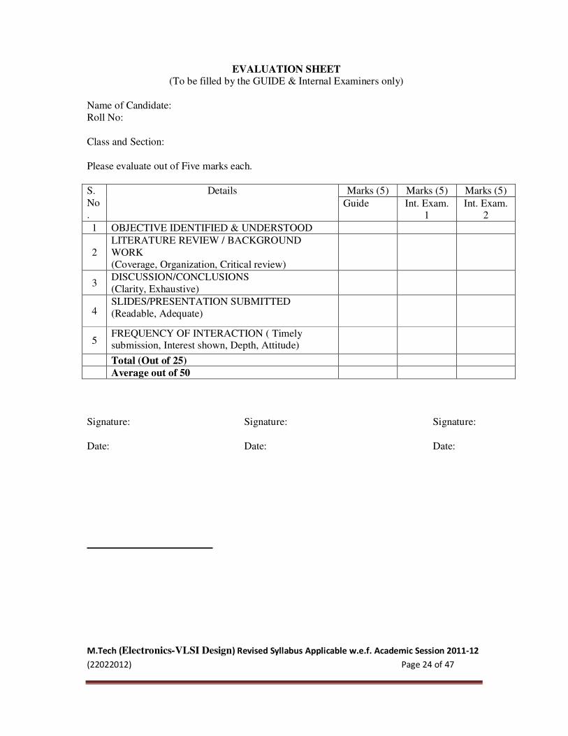
M.Tech (Electronics-VLSI Design) Revised Syllabus Applicable w.e.f. Academic Session 2011-12
(22022012) Page 24 of 47
EVALUATION SHEET
(To be filled by the GUIDE & Internal Examiners only)
Name of Candidate:
Roll No:
Class and Section:
Please evaluate out of Five marks each.
S.
No
.
Details Marks (5) Marks (5) Marks (5)
Guide Int. Exam. 1
Int. Exam. 2
1 OBJECTIVE IDENTIFIED & UNDERSTOOD
2
LITERATURE REVIEW / BACKGROUND
WORK
(Coverage, Organization, Critical review)
3 DISCUSSION/CONCLUSIONS
(Clarity, Exhaustive)
4 SLIDES/PRESENTATION SUBMITTED
(Readable, Adequate)
5 FREQUENCY OF INTERACTION ( Timely submission, Interest shown, Depth, Attitude)
Total (Out of 25)
Average out of 50
Signature: Signature: Signature:
Date: Date: Date:
M.Tech (Electronics-VLSI Design) Revised Syllabus Applicable w.e.f. Academic Session 2011-12
(22022012) Page 25 of 47
EVALUATION SHEET FOR EXTERNAL EXAMINER
(To be filled by the External Examiner only)
Name of Candidate:
Roll No :
I. For use by External Examiner ONLY
Please evaluate out of Ten marks each.
S.No. Details Marks (10)
1 OBJECTIVE IDENTIFIED & UNDERSTOOD
2 LITERATURE REVIEW / BACKGROUND WORK
(Coverage, Organization, Critical review)
3 DISCUSSION/CONCLUSIONS
(Clarity, Exhaustive)
4 POWER POINT PRESENTATION
(Clear, Structured)
5 SLIDES
(Readable, Adequate)
Total (Out of 50)
Signature:
Date:
M.Tech (Electronics-VLSI Design) Revised Syllabus Applicable w.e.f. Academic Session 2011-12
(22022012) Page 26 of 47
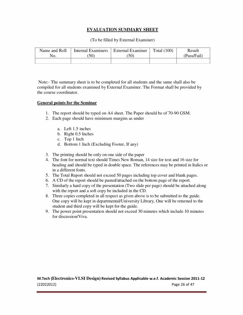
EVALUATION SUMMARY SHEET
(To be filled by External Examiner)
Name and Roll
No.
Internal Examiners
(50)
External Examiner
(50)
Total (100) Result
(Pass/Fail)
Note:- The summary sheet is to be completed for all students and the same shall also be
compiled for all students examined by External Examiner. The Format shall be provided by
the course coordinator.
General points for the Seminar
1. The report should be typed on A4 sheet. The Paper should be of 70-90 GSM.
2. Each page should have minimum margins as under
a. Left 1.5 inches
b. Right 0.5 Inches
c. Top 1 Inch
d. Bottom 1 Inch (Excluding Footer, If any)
3. The printing should be only on one side of the paper 4. The font for normal text should Times New Roman, 14 size for text and 16 size for
heading and should be typed in double space. The references may be printed in Italics or in a different fonts.
5. The Total Report should not exceed 50 pages including top cover and blank pages. 6. A CD of the report should be pasted/attached on the bottom page of the report.
7. Similarly a hard copy of the presentation (Two slide per page) should be attached along
with the report and a soft copy be included in the CD.
8. Three copies completed in all respect as given above is to be submitted to the guide.
One copy will be kept in departmental/University Library, One will be returned to the
student and third copy will be kept for the guide.
9. The power point presentation should not exceed 30 minutes which include 10 minutes
for discussion/Viva.
M.Tech (Electronics-VLSI Design) Revised Syllabus Applicable w.e.f. Academic Session 2011-12
(22022012) Page 27 of 47
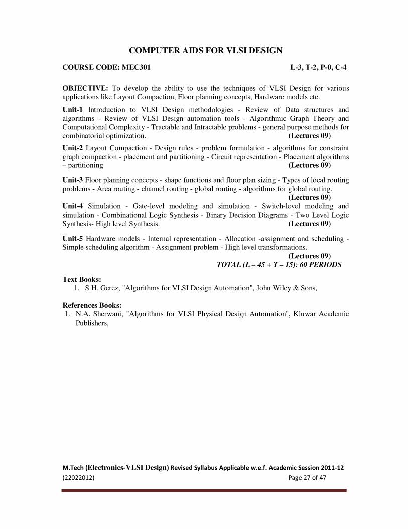
COMPUTER AIDS FOR VLSI DESIGN
COURSE CODE: MEC301 L-3, T-2, P-0, C-4
OBJECTIVE: To develop the ability to use the techniques of VLSI Design for various
applications like Layout Compaction, Floor planning concepts, Hardware models etc.
Unit-1 Introduction to VLSI Design methodologies - Review of Data structures and
algorithms - Review of VLSI Design automation tools - Algorithmic Graph Theory and
Computational Complexity - Tractable and Intractable problems - general purpose methods for
combinatorial optimization. (Lectures 09)
Unit-2 Layout Compaction - Design rules - problem formulation - algorithms for constraint
graph compaction - placement and partitioning - Circuit representation - Placement algorithms – partitioning (Lectures 09)
Unit-3 Floor planning concepts - shape functions and floor plan sizing - Types of local routing
problems - Area routing - channel routing - global routing - algorithms for global routing.
(Lectures 09)
Unit-4 Simulation - Gate-level modeling and simulation - Switch-level modeling and
simulation - Combinational Logic Synthesis - Binary Decision Diagrams - Two Level Logic
Synthesis- High level Synthesis. (Lectures 09)
Unit-5 Hardware models - Internal representation - Allocation -assignment and scheduling -
Simple scheduling algorithm - Assignment problem - High level transformations.
(Lectures 09)
TOTAL (L – 45 + T – 15): 60 PERIODS
Text Books: 1. S.H. Gerez, "Algorithms for VLSI Design Automation", John Wiley & Sons,
References Books:
1. N.A. Sherwani, "Algorithms for VLSI Physical Design Automation", Kluwar Academic
Publishers,
M.Tech (Electronics-VLSI Design) Revised Syllabus Applicable w.e.f. Academic Session 2011-12
(22022012) Page 28 of 47
INDUSTRIAL MANAGEMENT AND RESEARCH METHODOLOGY
[Amended vide approval dated 20th
November 2012]
Course Code: MHM 301 L-3, T-2, P-0, C-4
OBJECTIVE:
1) To enhance the knowledge of students in the area of Industrial Management, General
Management, Productivity, leadership and motivational skills.
2) To impart understanding of Research Methodology process, Hypothesis Testing and
statistical analysis.
UNIT-I (Lectures: 09)
Industrial management:-Introduction, Concept, Application & Scope. Productivity: Definition,
Measurement, Productivity Index, Types of production system
UNIT-II (Lectures: 09)
Management Function: Concept, Nature, Importance, Management: Art and Science,
Management skills, Levels of Management. Evolution of Management: Early contributions,
Taylors and scientific Management, Bureaucracy, Hawthorne Experiments and human
Relations, Social System Approach, Decision Theory Approach.
UNIT-III (Lectures: 09)
Organizational behaviour:- Concept, Nature, conceptual Foundations. Perception: Concept,
Nature, Processes, Importance; Motivation: Concept, Process, Theories of Motivation.
Leadership: Style & Theories of Leadership- Trait, Behavioral and Situational Theories;
Emotional Intelligence
UNIT-IV (Lectures: 09)
Research Methodology ; Concept of Research and its Application , Types of Research , Steps
involved in Research Processes , Collection of data : Types of Data -Primary & Secondary
data , Various Methods of Collection Of Data.; Concept of sample , Sample Size & Sampling
Procedure, Various Techniques of Sampling .Analysis of data : Coding , Editing and
Tabulation of data , Various kinds of Charts and Diagrams used in data Analysis .
UNIT-V (Lectures: 09)
M.Tech (Electronics-VLSI Design) Revised Syllabus Applicable w.e.f. Academic Session 2011-12
(22022012) Page 29 of 47
Estimation Theory and Hypothesis testing: Meaning & Characteristics of a good Hypothesis,
Formulation of Hypothesis, ways of stating a Hypothesis, test of significance, Level of
significance, Errors in Hypothesis- test I, test II Errors .Application of Z test , T test , F test
and chi-square test ,
TOTAL: (45 LECTURES + 15 TUTORIALS) =60 PERIODS
TEXT BOOKS:
1- Industrial Engineering and Production Management, M. MAHAJAN, Dhanpat Rai & Sons
2-Koontz Harold & W. Heinz- Essentials of Management (Tata Mc Graw Hill, Fifth Edition
2008)
3:- Robbins Stephen P. Organizational behavior (Pearson Education 13th Edition)
4-Cooper and Schindler- Business Research Methods (Tata McGraw Hill, 9th
Edition)
5:-Kothari CR- Research Methodology Methods and techniques (New age International
Publishers)
REFERENCE BOOKS:
1. Industrial Engineering and Management, O.P. KHANNA
2. Principles of Management. L.M.Prasad.
3. K.Aswathappa- Organizational behavior
4. Luthans Fred- Organizational behavior (Tata McGraw Hill, 10th
Edition)
5. Saunders- Research Methods for Business Students(Pearson Education ,2nd Edition)
6. Byod and others- marketiry Research (All India traveler Bookseller)
7. Beri .G.C- Statistics for management Tata Mc. Graw Hill.
8. Levin Rubin – Statistics for Management (Peasson 2000, new delhi, 7th
edition)
M.Tech (Electronics-VLSI Design) Revised Syllabus Applicable w.e.f. Academic Session 2011-12
(22022012) Page 30 of 47
CMOS RF CIRCUIT DESIGN (ELECTIVE)
COURSE CODE: MEC335 L-3, T-2, P-0, C-4
OBJECTIVE: To develop the ability to use the techniques of Design and Applications , Analog and digital modulation of RF circuits Operations Research for various applications,
BJT and MOSFET behavior at RF frequencies etc.
Unit-1 Design and Applications, Complexity and Choice of Technology. Basic concepts in RF
design: Nonlinearly and Time Variance, Intersymbol interference, random processes and
noise. Sensitivity and dynamic range, conversion of gains and distortion. (Lectures 09)
Unit-2 Analog and digital modulation of RF circuits, Comparison of various techniques for
power efficiency, Coherent and non-coherent detection, Mobile RF communication and basics
of Multiple Access techniques. Receiver and Transmitter architectures. Direct conversion and
two step transmitters. (Lectures 09)
Unit-3 RF testing for heterodyne, Homodyne, Image reject, Direct IF and sub sampled
receivers. BJT and MOSFET behavior at RF frequencies, Modeling of the transistors and SPICE model,
Noise performance and limitations of devices, integrated parasitic elements at high frequencies and their monolithic implementation. (Lectures 09)
Unit-4 Overview of RF Filter design, Active RF components & modeling, Matching and
Biasing Networks. Basic blocks in RF systems and their VLSI implementation, Low noise Amplifier design in various technologies, Design of Mixers at GHz frequency range, various
mixers working and implementation. Oscillators- Basic topologies VCO and definition of
phase noise, Noise power and trade off. Resonator VCO designs, Quadrature and single
sideband generators. (Lectures 09)
Unit-5 Radio frequency Synthesizers- PLLS, Various RF synthesizer architectures and
frequency dividers, Power Amplifier design, Liberalization techniques, Design issues in
integrated RF filters. (Lectures 09)
TOTAL (L – 45 + T – 15): 60 PERIODS
Text Book:
1. Thomas H. Lee “Design of CMOS RF Integrated Circuits” Cambridge University press.
References Book:
1. B. Razavi “RF Microelectronics” PHI
2. R. Jacob Baker, H.W. Li, D.E. Boyce “ CMOS Circiut Design, layout and Simulation” PHI
3.Y.P. Tsividis “Mixed Analog and Digital Devices and Technology” TMH
M.Tech (Electronics-VLSI Design) Revised Syllabus Applicable w.e.f. Academic Session 2011-12
(22022012) Page 31 of 47
DESIGN OF SEMICONDUCTOR MEMORIES (ELECTIVE)
COURSE CODE: MEC336 L-3, T-2, P-0, C-4
OBJECTIVE: To develop the ability to use the techniques of Masked Read-Only Memories
(ROMs)-High Density ROMs-Programmable Read-Only Memories applications like DRAM
Technology Development, RAM Fault Modeling, Electrical Testing etc.
Unit-1 SRAM Cell Structures-MOS SRAM Architecture-MOS SRAM Cell and Peripheral
Circuit Operation-Bipolar SRAM Technologies-Silicon On Insulator (SOl) Technology-
Advanced SRAM Architectures and Technologies-Application Specific SRAMs.
(Lectures 09) Unit-2 DRAM Technology Development-CMOS DRAMs - DRAMs Cell Theory and
Advanced Cell Strucutures - BiCMOS, DRAMs - Soft Error Failures in DRAMs - Advanced
DRAM Designs and Architecture-Application Specific DRAMs. (Lectures 09)
Unit-3 Masked Read-Only Memories (ROMs)-High Density ROMs-Programmable Read-
Only Memories (PROMs)-Bipolar PROMs-CMOS PROMs-Erasable (UV) - Programmable
Road-Only Memories (EPROMs)-Floating-Gate EPROM Cell-One-Time Programmable
(OTP) Eproms-Electrically Erasable PROMs (EEPROMs)-EEPROM Technology And Architecture-Nonvolatile SRAM-Flash Memories (EPROMs or EEPROM)-Advanced Flash
Memory Architecture. (Lectures 09)
Unit-4 RAM Fault Modelling, Electrical Testing, Pseudo Random Testing-Megabit DRAM Testing-Non-volatile Memory Modelling and Testing-IDDQ Fault Modelling and Testing-
Application Specific Memory Testing. (Lectures 09)
Unit-5 General Reliability Issues-RAM Failure Modes and Mechanism-Non-volatile Memory
Reliability-Reliability Modelling and Failure Rate Prediction-Design for Reliability-Reliability
Test Structures-Reliability Screening and Qualification. RAM Fault Modelling, Electrical
Testing, Pseudo Random Testing-Megabit DRAM Testing-Non-volatile Memory Modelling
and Testing-IDDQ Fault Modelling and Testing-Application Specific Memory Testing.
(Lectures 09)
TOTAL (L – 45 + T – 15): 60 PERIODS
Text Books:
1. Ashok K. Sharma, "Semiconductor Memories", Two-Volume Set, Wiley-IEEE Press,
2. Brent Keeth, R. Jacob Baker, "DRAM Circuit Design: A Tutorial", Wiley-IEEE Press.
Reference Books:
1. Betty Prince, "High Performance Memories: New Architecture DRAMs and SRAMs
Evolution and Function", Wiley,
M.Tech (Electronics-VLSI Design) Revised Syllabus Applicable w.e.f. Academic Session 2011-12
(22022012) Page 32 of 47
FPGA/CPLD BASED SYSTEMS
COURSE CODE: MEC 333 L-3, T-2, P-0, C-4
OBJECTIVE: To develop the ability to use the techniques of like Digital Design and FPGAs,
Hardware Description Languages, Sequential Machines etc.
Unit 1 Introduction. Basic Concepts. Digital Design and FPGAs. FPGA-Based System
Design. Summary. Problems. (Lectures 09)
Unit 2 VLSI Technology behind FPGA/CPLD, Manufacturing Processes. CMOS Logic Gates. Wires, Registers and RAM, Packages and Pads. (Lectures 09)
Unit 3 FPGA Fabrics. FPGA Architectures. SRAM-Based FPGAs. Permanently Programmed
FPGAs. Chip I/O. Circuit Design of FPGA Fabrics. Architecture of FPGA Fabrics.
(Lectures 09)
Unit 4 Combinational Logic, The Logic Design Process. Hardware Description Languages.
Combinational Network Delay. Power and Energy Optimization. Arithmetic Logic. Logic Implementation for FPGAs. Physical Design for FPGAs. The Logic Design Process Revisited.
Summary. Problems. (Lectures 09)
Unit 5 Sequential Machines, The Sequential Machine Design Process. Sequential Design Styles. Rules for Clocking. Performance Analysis. Power Optimization, Architecture,
Behavioral Design. Design Methodologies. (Lectures 09)
TOTAL (L – 45 + T – 15): 60 PERIODS
Text Books: 1. FPGA-Based System Design Wayne Wolf, Verlag: Prentice Hall PTR
Reference Books: 1. Modern VLSI Design: System-on-Chip Design (3rd Edition) (3RD) Wayne Wolf
M.Tech (Electronics-VLSI Design) Revised Syllabus Applicable w.e.f. Academic Session 2011-12
(22022012) Page 33 of 47
DIGITAL IMAGE PROCESSING
COURSE CODE: MEC334 L-3, T-2, P-0, C-4
OBJECTIVE: To study the image fundamentals and mathematical transform, image enhancement techniques, image restoration procedures, the image compression procedures,
the image segmentation and representation techniques.
UNIT I Elements of visual perception – Image sampling and quantization Basic relationship
between pixels – Basic geometric transformations-Introduction to Fourier Transform and DFT
– Properties of 2D Fourier Transform – FFT – Separable Image Transforms -Walsh –
Hadamard – Discrete Cosine Transform, Haar, Slant – Karhunen – Loeve transforms.
(Lectures 09)
UNIT II Spatial Domain methods: Basic grey level transformation – Histogram equalization –
Image subtraction – Image averaging –Spatial filtering: Smoothing, sharpening filters –
Laplacian filters – Frequency domain filters : Smoothing – Sharpening filters – Homomorphic
filtering. (Lectures 09)
UNIT III Model of Image Degradation/restoration process – Noise models – Inverse filtering -
Least mean square filtering – Constrained least mean square filtering – Blind image restoration
– Pseudo inverse – Singular value decomposition. (Lectures 09)
UNIT IV Lossless compression: Variable length coding – LZW coding – Bit plane coding- predictive coding-DPCM. Lossy Compression: Transform coding – Wavelet coding – Basics
of Image compression standards: JPEG, MPEG,Basics of Vector quantization. (Lectures 09)
UNIT V Edge detection – Thresh holding - Region Based segmentation – Boundary
representation: chair codes- Polygonal approximation – Boundary segments – boundary
descriptors: Simple descriptors-Fourier descriptors - Regional descriptors –Simple descriptors-
Texture. (Lectures 09)
TOTAL (L – 45 + T – 15): 60 PERIODS
TEXT BOOKS 1. Rafael C Gonzalez, Richard E Woods 2nd Edition, Digital Image Processing - Pearson
Education. 2. A.K. Jain, PHI, New Delhi -Fundamentals of Digital Image Processing.
3. Chanda Dutta Magundar – Digital Image Processing and Applications, Prentice Hall of
India,
REFERENCE BOOKS:
1. William K Pratt, Digital Image Processing John Willey
2. Image Processing Analysis and Machine Vision – Millman Sonka, Vaclav havac, Roger Boyle, Broos/colic, Thompson Learniy
M.Tech (Electronics-VLSI Design) Revised Syllabus Applicable w.e.f. Academic Session 2011-12
(22022012) Page 34 of 47
CAD VLSI (LAB)
L-0, T-0, P-4, C-2 COURSE CODE: MEC351
List of Experiments:
1. Fault tolerance measurement of two level combinational circuit.
2. Logical fault testing (bridging fault) of three level combinational circuit.
3. Design and simulation of ALU architecture using Xilinx FPGA.
4. Layout and simulation of CMOS amplifier.
5. Layout and simulation of Memories structure.
6. Design and simulation of Silicon accelerometer using MEMS CAD TOOL.
7. Design and simulation of pressure sensor using MEMS CAD TOOL.
8. Parametric extraction of a given device using VLSI CAD TOOL.
M.Tech (Electronics-VLSI Design) Revised Syllabus Applicable w.e.f. Academic Session 2011-12
(22022012) Page 35 of 47
MINOR PROJECT
COURSE CODE: MEC 391 L-0, T-0, P-4, C-2
Objective: Various hardware / software projects will be given to the students to enhance the
designing and analyzing capability required in VLSI industry.
M.Tech (Electronics-VLSI Design) Revised Syllabus Applicable w.e.f. Academic Session 2011-12
(22022012) Page 36 of 47
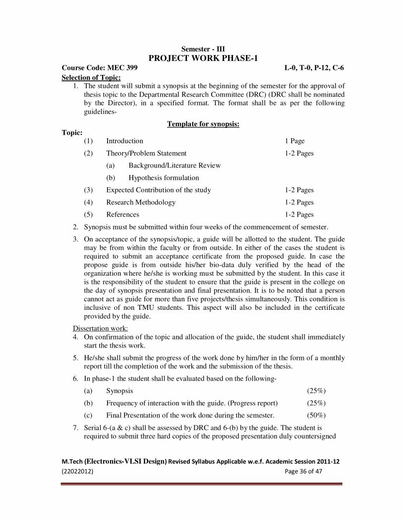
Semester - III
PROJECT WORK PHASE-1 Course Code: MEC 399 L-0, T-0, P-12, C-6
Selection of Topic: 1. The student will submit a synopsis at the beginning of the semester for the approval of
thesis topic to the Departmental Research Committee (DRC) (DRC shall be nominated by the Director), in a specified format. The format shall be as per the following
guidelines-
Template for synopsis:
Topic: (1) Introduction 1 Page
(2) Theory/Problem Statement 1-2 Pages
(a) Background/Literature Review
(b) Hypothesis formulation
(3) Expected Contribution of the study 1-2 Pages
(4) Research Methodology 1-2 Pages
(5) References 1-2 Pages
2. Synopsis must be submitted within four weeks of the commencement of semester.
3. On acceptance of the synopsis/topic, a guide will be allotted to the student. The guide
may be from within the faculty or from outside. In either of the cases the student is
required to submit an acceptance certificate from the proposed guide. In case the
propose guide is from outside his/her bio-data duly verified by the head of the
organization where he/she is working must be submitted by the student. In this case it
is the responsibility of the student to ensure that the guide is present in the college on
the day of synopsis presentation and final presentation. It is to be noted that a person
cannot act as guide for more than five projects/thesis simultaneously. This condition is
inclusive of non TMU students. This aspect will also be included in the certificate
provided by the guide.
Dissertation work:
4. On confirmation of the topic and allocation of the guide, the student shall immediately
start the thesis work.
5. He/she shall submit the progress of the work done by him/her in the form of a monthly report till the completion of the work and the submission of the thesis.
6. In phase-1 the student shall be evaluated based on the following-
(a) Synopsis (25%)
(b) Frequency of interaction with the guide. (Progress report) (25%)
(c) Final Presentation of the work done during the semester. (50%)
7. Serial 6-(a & c) shall be assessed by DRC and 6-(b) by the guide. The student is required to submit three hard copies of the proposed presentation duly countersigned
M.Tech (Electronics-VLSI Design) Revised Syllabus Applicable w.e.f. Academic Session 2011-12
(22022012) Page 37 of 47
by the guide to the departmental head. Student should generally restrict him/her self to
the presentation slide submitted by him/her.
M.Tech (Electronics-VLSI Design) Revised Syllabus Applicable w.e.f. Academic Session 2011-12
(22022012) Page 38 of 47
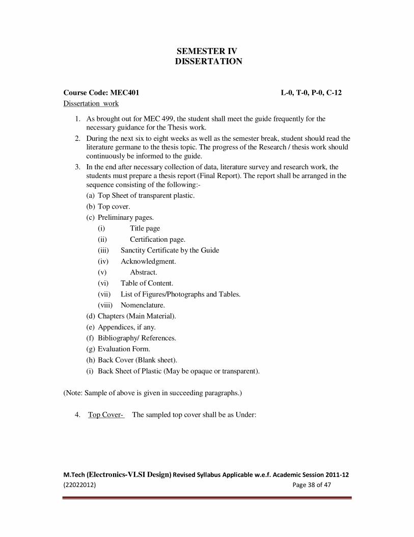
SEMESTER IV
DISSERTATION
Course Code: MEC401 L-0, T-0, P-0, C-12
Dissertation work
1. As brought out for MEC 499, the student shall meet the guide frequently for the necessary guidance for the Thesis work.
2. During the next six to eight weeks as well as the semester break, student should read the literature germane to the thesis topic. The progress of the Research / thesis work should
continuously be informed to the guide.
3. In the end after necessary collection of data, literature survey and research work, the
students must prepare a thesis report (Final Report). The report shall be arranged in the
sequence consisting of the following:-
(a) Top Sheet of transparent plastic.
(b) Top cover.
(c) Preliminary pages.
(i) Title page
(ii) Certification page.
(iii) Sanctity Certificate by the Guide
(iv) Acknowledgment.
(v) Abstract.
(vi) Table of Content.
(vii) List of Figures/Photographs and Tables.
(viii) Nomenclature.
(d) Chapters (Main Material).
(e) Appendices, if any.
(f) Bibliography/ References.
(g) Evaluation Form.
(h) Back Cover (Blank sheet).
(i) Back Sheet of Plastic (May be opaque or transparent).
(Note: Sample of above is given in succeeding paragraphs.)
4. Top Cover- The sampled top cover shall be as Under:
M.Tech (Electronics-VLSI Design) Revised Syllabus Applicable w.e.f. Academic Session 2011-12
(22022012) Page 39 of 47
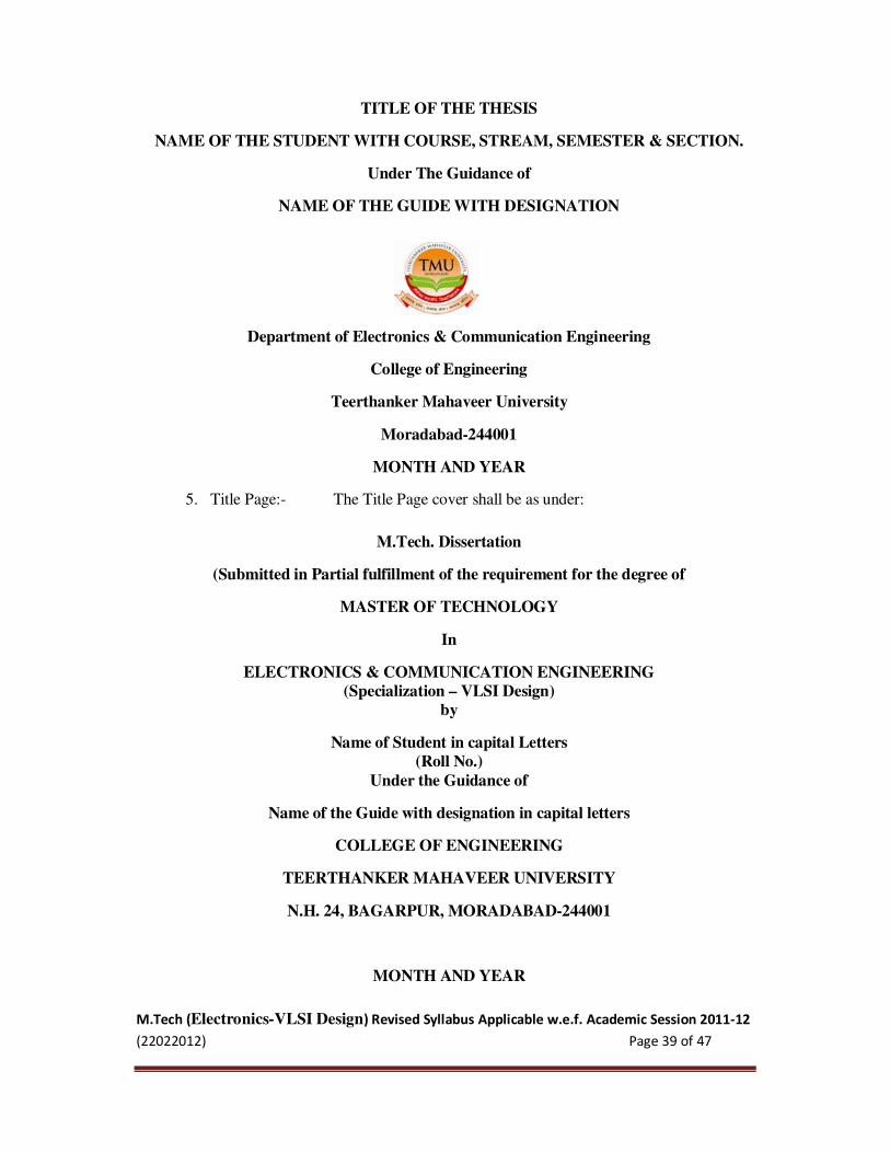
TITLE OF THE THESIS
NAME OF THE STUDENT WITH COURSE, STREAM, SEMESTER & SECTION.
Under The Guidance of
NAME OF THE GUIDE WITH DESIGNATION
Department of Electronics & Communication Engineering
College of Engineering
Teerthanker Mahaveer University
Moradabad-244001
MONTH AND YEAR
5. Title Page:- The Title Page cover shall be as under:
M.Tech. Dissertation
(Submitted in Partial fulfillment of the requirement for the degree of
MASTER OF TECHNOLOGY
In
ELECTRONICS & COMMUNICATION ENGINEERING
(Specialization – VLSI Design)
by
Name of Student in capital Letters
(Roll No.)
Under the Guidance of
Name of the Guide with designation in capital letters
COLLEGE OF ENGINEERING
TEERTHANKER MAHAVEER UNIVERSITY
N.H. 24, BAGARPUR, MORADABAD-244001
MONTH AND YEAR
M.Tech (Electronics-VLSI Design) Revised Syllabus Applicable w.e.f. Academic Session 2011-12
(22022012) Page 40 of 47
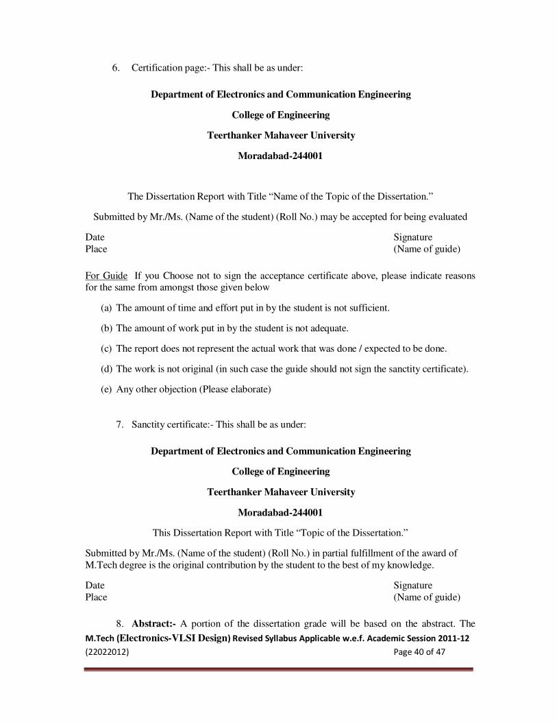
6. Certification page:- This shall be as under:
Department of Electronics and Communication Engineering
College of Engineering
Teerthanker Mahaveer University
Moradabad-244001
The Dissertation Report with Title “Name of the Topic of the Dissertation.”
Submitted by Mr./Ms. (Name of the student) (Roll No.) may be accepted for being evaluated
Date Signature
Place (Name of guide)
For Guide If you Choose not to sign the acceptance certificate above, please indicate reasons for the same from amongst those given below
(a) The amount of time and effort put in by the student is not sufficient.
(b) The amount of work put in by the student is not adequate.
(c) The report does not represent the actual work that was done / expected to be done.
(d) The work is not original (in such case the guide should not sign the sanctity certificate).
(e) Any other objection (Please elaborate)
7. Sanctity certificate:- This shall be as under:
Department of Electronics and Communication Engineering
College of Engineering
Teerthanker Mahaveer University
Moradabad-244001
This Dissertation Report with Title “Topic of the Dissertation.”
Submitted by Mr./Ms. (Name of the student) (Roll No.) in partial fulfillment of the award of
M.Tech degree is the original contribution by the student to the best of my knowledge.
Date Signature
Place (Name of guide)
8. Abstract:- A portion of the dissertation grade will be based on the abstract. The
M.Tech (Electronics-VLSI Design) Revised Syllabus Applicable w.e.f. Academic Session 2011-12
(22022012) Page 41 of 47
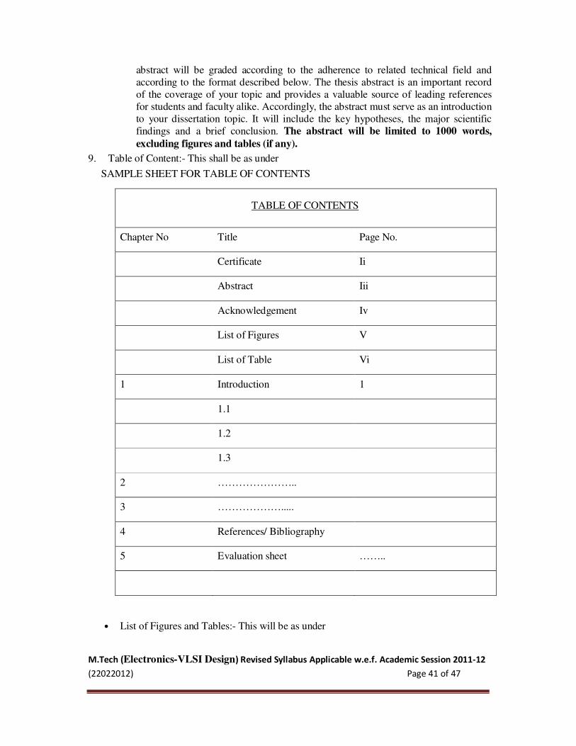
abstract will be graded according to the adherence to related technical field and
according to the format described below. The thesis abstract is an important record
of the coverage of your topic and provides a valuable source of leading references
for students and faculty alike. Accordingly, the abstract must serve as an introduction
to your dissertation topic. It will include the key hypotheses, the major scientific
findings and a brief conclusion. The abstract will be limited to 1000 words,
excluding figures and tables (if any).
9. Table of Content:- This shall be as under
SAMPLE SHEET FOR TABLE OF CONTENTS
TABLE OF CONTENTS
Chapter No Title Page No.
Certificate Ii
Abstract Iii
Acknowledgement Iv
List of Figures V
List of Table Vi
1 Introduction 1
1.1
1.2
1.3
2 …………………..
3 ……………….....
4 References/ Bibliography
5 Evaluation sheet ……..
• List of Figures and Tables:- This will be as under
M.Tech (Electronics-VLSI Design) Revised Syllabus Applicable w.e.f. Academic Session 2011-12
(22022012) Page 42 of 47
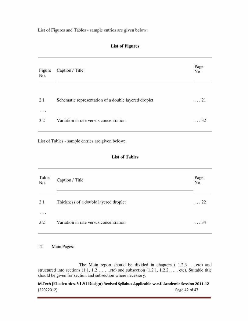
List of Figures and Tables - sample entries are given below:
List of Figures
Figure
No.
Caption / Title
Page
No.
2.1 Schematic representation of a double layered droplet . . . 21
. . .
3.2 Variation in rate versus concentration . . . 32
List of Tables - sample entries are given below:
List of Tables
Table No.
Caption / Title
Page No.
2.1 Thickness of a double layered droplet . . . 22
. . .
3.2 Variation in rate versus concentration . . . 34
12. Main Pages:-
The Main report should be divided in chapters ( 1,2,3 …..etc) and
structured into sections (1.1, 1.2 ……..etc) and subsection (1.2.1, 1.2.2, ….. etc). Suitable title
should be given for section and subsection where necessary.
M.Tech (Electronics-VLSI Design) Revised Syllabus Applicable w.e.f. Academic Session 2011-12
(22022012) Page 43 of 47
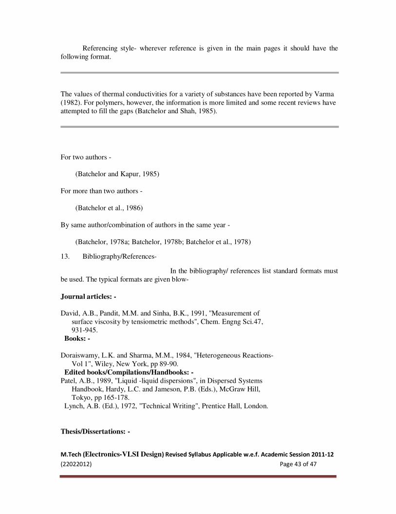
Referencing style- wherever reference is given in the main pages it should have the
following format.
The values of thermal conductivities for a variety of substances have been reported by Varma
(1982). For polymers, however, the information is more limited and some recent reviews have
attempted to fill the gaps (Batchelor and Shah, 1985).
For two authors -
(Batchelor and Kapur, 1985)
For more than two authors -
(Batchelor et al., 1986)
By same author/combination of authors in the same year -
(Batchelor, 1978a; Batchelor, 1978b; Batchelor et al., 1978)
13. Bibliography/References-
In the bibliography/ references list standard formats must
be used. The typical formats are given blow-
Journal articles: -
David, A.B., Pandit, M.M. and Sinha, B.K., 1991, "Measurement of
surface viscosity by tensiometric methods", Chem. Engng Sci.47,
931-945.
Books: -
Doraiswamy, L.K. and Sharma, M.M., 1984, "Heterogeneous Reactions-
Vol 1", Wiley, New York, pp 89-90.
Edited books/Compilations/Handbooks: -
Patel, A.B., 1989, "Liquid -liquid dispersions", in Dispersed Systems
Handbook, Hardy, L.C. and Jameson, P.B. (Eds.), McGraw Hill,
Tokyo, pp 165-178.
Lynch, A.B. (Ed.), 1972, "Technical Writing", Prentice Hall, London.
Thesis/Dissertations: -
M.Tech (Electronics-VLSI Design) Revised Syllabus Applicable w.e.f. Academic Session 2011-12
(22022012) Page 44 of 47
Pradhan, S.S., 1992, "Hydrodynamic and mass transfer characteristics of packed extraction
columns", Ph.D. Thesis, University of Manchester, Manchester, U.K.
Citations from abstracts: -
Lee, S. and Demlow, B.X., 1985, US Patent 5,657,543, Cf C.A. 56, 845674.
Personal Communications: -
Reddy, A.R., 1993, personal communication at private meeting on 22 October 1992 at Physics
Department, Indian Institute of Technology, Delhi.
Electronic sources (web material and the like):
For citing web pages and electronic documents, use the APA style given at:
http://www.apastyle.org/elecsource.html
14. Evaluation Form: - Three sheets of evaluation form should be attached in the report as
under.
a. Evaluation form for guide and other Internal Examiner.
b. Evaluation form for external examiners.
c. Summary Sheet
15. Evaluation form for Guide & Internal Examiners:-
M.Tech (Electronics-VLSI Design) Revised Syllabus Applicable w.e.f. Academic Session 2011-12
(22022012) Page 45 of 47
EVALUATION SHEET
(To be filled by the Guide & Internal Examiners only)
Name of Candidate:
Roll No:
Class and Section:
Please evaluate out of five marks each.
S.
No
.
Details Marks (5) Marks (5) Marks (5)
Guide Int. Exam.
1
Int. Exam.
2
1 OBJECTIVE IDENTIFIED & UNDERSTOOD
2
LITERATURE REVIEW / BACKGROUND
WORK
(Coverage, Organization, Critical review)
3 DISCUSSION/CONCLUSIONS
(Clarity, Exhaustive)
4 SLIDES/PRESENTATION SUBMITTED
(Readable, Adequate)
5 FREQUENCY OF INTERACTION ( Timely
submission, Interest shown, Depth, Attitude)
Total (Out of 25)
Average out of 50
Signature: Signature: Signature:
Date: Date: Date:
M.Tech (Electronics-VLSI Design) Revised Syllabus Applicable w.e.f. Academic Session 2011-12
(22022012) Page 46 of 47
EVALUATION SHEET FOR EXTERNAL EXAMINER
(To be filled by the External Examiner only)
Name of Candidate:
Roll No :
I. For use by External Examiner ONLY
Please evaluate out of ten marks each.
S.No. Details Marks (10)
1 OBJECTIVE IDENTIFIED & UNDERSTOOD
2 LITERATURE REVIEW / BACKGROUND WORK
(Coverage, Organization, Critical review)
3 DISCUSSION/CONCLUSIONS
(Clarity, Exhaustive)
4 POWER POINT PRESENTATION
(Clear, Structured)
5 SLIDES
(Readable, Adequate)
Total (Out of 50)
Signature:
Date:
EVALUATION SUMMARY SHEET
(To be filled by External Examiner)
Name and Roll
No.
Internal Examiners
(50)
External Examiner
(50)
Total (100) Result
(Pass/Fail)
Note:- The summary sheet is to be completed for all students and the same shall also be
compiled for all students examined by External Examiner. The Format shall be provided by
the course coordinator.
General points for the Dissertation
10. The report should be typed on A4 sheet. The Paper should be of 70-90 GSM. 11. Each page should have minimum margins as under
e. Left 1.5 inches
f. Right 0.5 Inches
g. Top 1 Inch
h. Bottom 1 Inch (Excluding Footer, If any)
M.Tech (Electronics-VLSI Design) Revised Syllabus Applicable w.e.f. Academic Session 2011-12
(22022012) Page 47 of 47
12. The printing should be only on one side of the paper
13. The font for normal text should be Times New Roman, 14 size for text and 16 size for
heading and should be typed in double space. The references may be printed in Italics or
in different fonts.
14. The Total Report should not exceed 50 pages including top cover and blank pages.
15. A CD of the report should be pasted/ attached on the bottom page of the report.
16. Similarly a hard copy of the presentation (Two slides per page) should be attached along with the report and a soft copy should be included in the CD.
17. Three copies completed in all respect (as given above) are to be submitted to the guide. One copy will be kept in departmental/University Library, One will be returned to the
student and third copy will be for the guide. 18. The power point presentation should not exceed 30 minutes which include 10 minutes
for discussion/Viva.