Embed Size (px)
Citation preview
Master of Technology
In
Electronics & Communication Engineering (VLSI Design Automation and Techniques)
Course Structure & Syllabus
Department of Electronics & Communication Engineering
National Institute of Technology Hamirpur
Hamirpur (HP) – 177005, India
Electronics and Communication Engineering 2
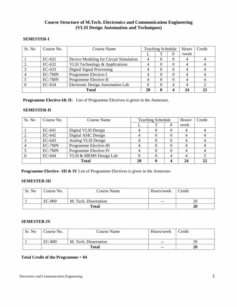
Course Structure of M.Tech. Electronics and Communication Engineering
(VLSI Design Automation and Techniques)
SEMESTER-I
Sr. No Course No. Course Name Teaching Schedule Hours
/week
Credit
L T P
1 EC-631 Device Modeling for Circuit Simulation 4 0 0 4 4
2 EC-632 VLSI Technology & Applications 4 0 0 4 4
3 EC-633 Digital Signal Processing 4 0 0 4 4
4 EC-7MN Programme Elective-I 4 0 0 4 4
5 EC-7MN Programme Elective-II 4 0 0 4 4
6 EC-634 Electronic Design Automation Lab 0 0 4 4 2
Total 20 0 4 24 22
Programme Elective-I& II: List of Programme Electives is given in the Annexure.
SEMESTER-II
Sr. No Course No. Course Name Teaching Schedule Hours/
week
Credit
L T P
1 EC-641 Digital VLSI Design 4 0 0 4 4
2 EC-642 Digital ASIC Design 4 0 0 4 4
3 EC-643 Analog VLSI Design 4 0 0 4 4
4 EC-7MN Programme Elective-III 4 0 0 4 4
5 EC-7MN Programme Elective-IV 4 0 0 4 4
6 EC-644 VLSI & MEMS Design Lab 0 0 4 4 2
Total 20 0 4 24 22
Programme Elective –III & IV List of Programme Electives is given in the Annexure.
SEMESTER-III
Sr. No Course No. Course Name Hours/week Credit
1 EC-800 M. Tech. Dissertation -- 20
Total 20
SEMESTER-IV
Sr. No Course No. Course Name Hours/week Credit
1 EC-800 M. Tech. Dissertation -- 20
Total -- 20
Total Credit of the Programme = 84
Electronics and Communication Engineering 3
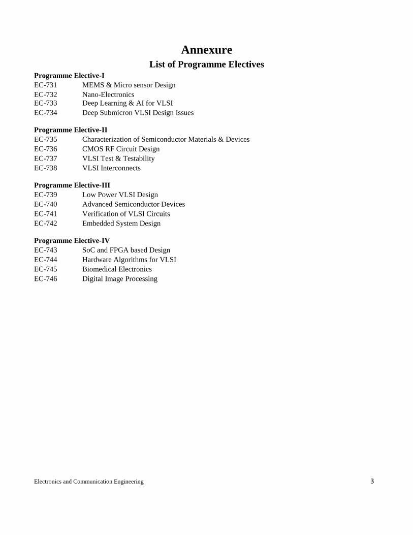
Annexure
List of Programme Electives
Programme Elective-I
EC-731 MEMS & Micro sensor Design
EC-732 Nano-Electronics
EC-733 Deep Learning & AI for VLSI
EC-734 Deep Submicron VLSI Design Issues
Programme Elective-II
EC-735 Characterization of Semiconductor Materials & Devices
EC-736 CMOS RF Circuit Design
EC-737 VLSI Test & Testability
EC-738 VLSI Interconnects
Programme Elective-III
EC-739 Low Power VLSI Design
EC-740 Advanced Semiconductor Devices
EC-741 Verification of VLSI Circuits
EC-742 Embedded System Design
Programme Elective-IV
EC-743 SoC and FPGA based Design
EC-744 Hardware Algorithms for VLSI
EC-745 Biomedical Electronics
EC-746 Digital Image Processing
Electronics and Communication Engineering 4
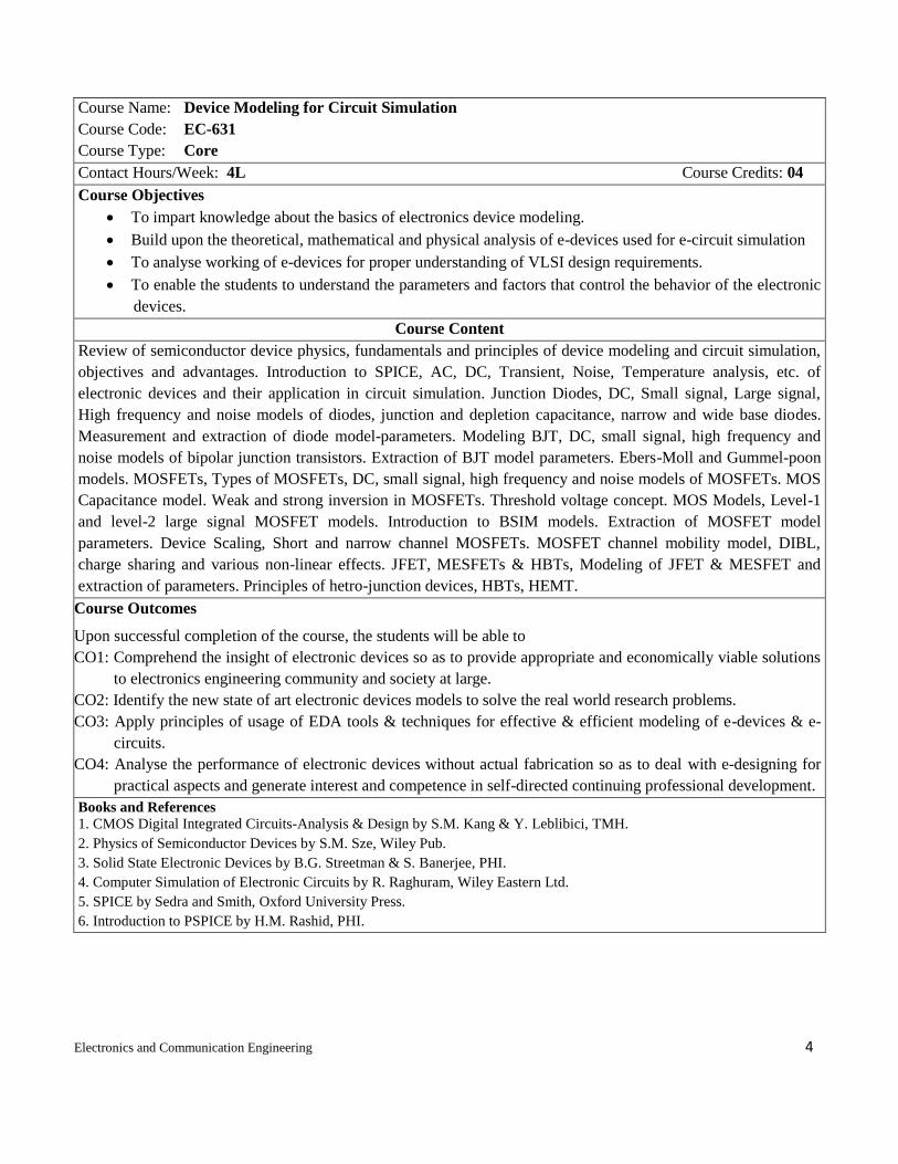
Course Name: Device Modeling for Circuit Simulation
Course Code: EC-631
Course Type: Core
Contact Hours/Week: 4L Course Credits: 04
Course Objectives
To impart knowledge about the basics of electronics device modeling.
Build upon the theoretical, mathematical and physical analysis of e-devices used for e-circuit simulation
To analyse working of e-devices for proper understanding of VLSI design requirements.
To enable the students to understand the parameters and factors that control the behavior of the electronic
devices.
Course Content
Review of semiconductor device physics, fundamentals and principles of device modeling and circuit simulation,
objectives and advantages. Introduction to SPICE, AC, DC, Transient, Noise, Temperature analysis, etc. of
electronic devices and their application in circuit simulation. Junction Diodes, DC, Small signal, Large signal,
High frequency and noise models of diodes, junction and depletion capacitance, narrow and wide base diodes.
Measurement and extraction of diode model-parameters. Modeling BJT, DC, small signal, high frequency and
noise models of bipolar junction transistors. Extraction of BJT model parameters. Ebers-Moll and Gummel-poon
models. MOSFETs, Types of MOSFETs, DC, small signal, high frequency and noise models of MOSFETs. MOS
Capacitance model. Weak and strong inversion in MOSFETs. Threshold voltage concept. MOS Models, Level-1
and level-2 large signal MOSFET models. Introduction to BSIM models. Extraction of MOSFET model
parameters. Device Scaling, Short and narrow channel MOSFETs. MOSFET channel mobility model, DIBL,
charge sharing and various non-linear effects. JFET, MESFETs & HBTs, Modeling of JFET & MESFET and
extraction of parameters. Principles of hetro-junction devices, HBTs, HEMT.
Course Outcomes
Upon successful completion of the course, the students will be able to
CO1: Comprehend the insight of electronic devices so as to provide appropriate and economically viable solutions
to electronics engineering community and society at large.
CO2: Identify the new state of art electronic devices models to solve the real world research problems.
CO3: Apply principles of usage of EDA tools & techniques for effective & efficient modeling of e-devices & e-
circuits.
CO4: Analyse the performance of electronic devices without actual fabrication so as to deal with e-designing for
practical aspects and generate interest and competence in self-directed continuing professional development.
Books and References
1. CMOS Digital Integrated Circuits-Analysis & Design by S.M. Kang & Y. Leblibici, TMH.
2. Physics of Semiconductor Devices by S.M. Sze, Wiley Pub.
3. Solid State Electronic Devices by B.G. Streetman & S. Banerjee, PHI.
4. Computer Simulation of Electronic Circuits by R. Raghuram, Wiley Eastern Ltd.
5. SPICE by Sedra and Smith, Oxford University Press.
6. Introduction to PSPICE by H.M. Rashid, PHI.
Electronics and Communication Engineering 5
Course Name: VLSI Technology & Applications
Course Code: EC-632
Course Type: Core
Contact Hours/Week: 4L Course Credits: 04
Course Objectives
To introduce the VLSI era
To impart knowledge about the miniaturization of Electronic Systems.
To introduce the fundamental concepts relevant to VLSI fabrication.
To enable the students to understand the various VLSI fabrication techniques.
Course Content
Crystal growth: Source of silicon; Single crystalline and Poly crystalline; Requirement of purity for electronics
industry; Electronics grade silicon production; Crystal growth techniques: Bridgeman method, float zone method,
Czocharalski method, Modified Czocharalski method; refining; Silicon Wafer Preparation & Crystal Defects;
Epitaxial Process: Need of epitaxial layer; vapors phase epitaxy -reactor design, chemistry of epitaxial process,
transport mechanism doping & auto doping; selective epitaxy, epitaxial process induced defects, molecular beam
epitaxy, merits and demerits among epitaxial processes; recent trends in Epitaxy; Oxidation: Importance of
oxidation; types of oxidation techniques; growth mechanism & kinetics; factors affecting the growth mechanisms;
silicon oxidation model, dry & wet oxidation; oxidation induced faults; recent trends in oxidation; Lithography:
Basic steps in lithography; lithography techniques-optical lithography, electron beam lithography, x-ray lithography,
ion beam lithography; resists and mask preparation of respective lithographies, printing techniques-contact,
proximity printing and projection printing; merits and demerits of lithographies; recent trends in lithography at nano
regime; Etching: Performance metrics of etching; types of etching- wet and dry etching; dry etching techniques-ion
beam or ion-milling, sputter ion plasma etching and reactive ion etching (RIE); merits and demerits of etching;
etching induced defects; recent trends in etching; Diffusion and Ion Implantation: Diffusion mechanisms; diffusion
reactor; diffusion profile; diffusion kinetics; parameters affecting diffusion profile; Dopants and their behavior,
choice of dopants; Ion Implantation- reactor design, impurity distribution profile, properties of ion implantation, low
energy and high energy ion implantation; Metallization: Desired properties of metallization for VLSI; metallization
choices; metallization techniques –vacuum evaporation, sputtering; Assembly Techniques & Packaging of VLSI
chip: Introduction to packaging; packaging process; package design considerations, various package types, Prototype
fabrication of Monolithic Components and isolation : Prototype fabrication of Diodes, npn BJT, pnp BJT, MOSFETs
(Enhancement and depletion mode), n-MOS, p-MOS, CMOS, Resistors and Capacitors. Isolation techniques in
Diodes, BJT and MOSFETs (Enhancement and depletion mode.
Course Outcomes
Upon successful completion of the course, the students will be able to
CO1: Identify the various design limits material used for fabrication.
CO2: Describe the Performance of technology scaling.
CO3: Understand the complexities involved in the integrated circuits.
CO4: Apply principles to Identify and Analyze the various steps for the fabrication of various components
CO5: Assess the various reliability issues in VLSI technology
Books and References
1. VLSI Technology by S.M. Sze, TMH.
2. VLSI Fabrication Principles by S.K. Gandhi, John Willey& Sons.
3. Micromachined transducer by G.T.A. Kovacs, McGraw Hill.
Electronics and Communication Engineering 6
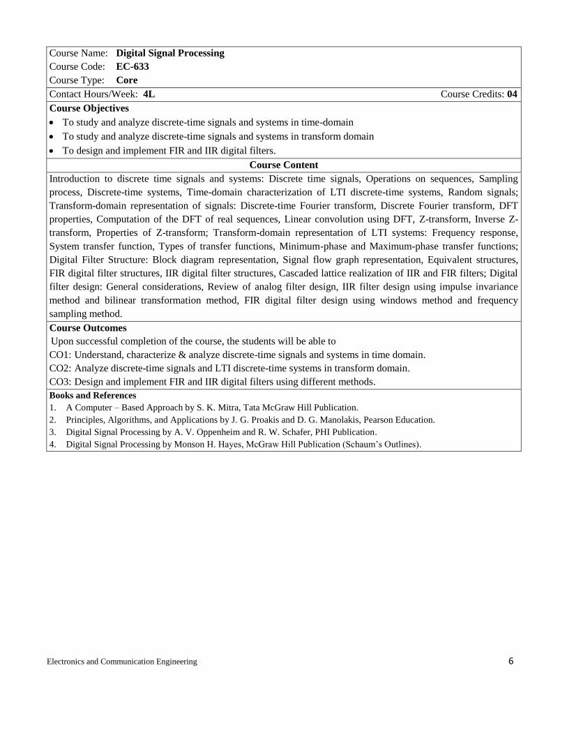
Course Name: Digital Signal Processing
Course Code: EC-633
Course Type: Core
Contact Hours/Week: 4L Course Credits: 04
Course Objectives
To study and analyze discrete-time signals and systems in time-domain
To study and analyze discrete-time signals and systems in transform domain
To design and implement FIR and IIR digital filters.
Course Content
Introduction to discrete time signals and systems: Discrete time signals, Operations on sequences, Sampling
process, Discrete-time systems, Time-domain characterization of LTI discrete-time systems, Random signals;
Transform-domain representation of signals: Discrete-time Fourier transform, Discrete Fourier transform, DFT
properties, Computation of the DFT of real sequences, Linear convolution using DFT, Z-transform, Inverse Z-
transform, Properties of Z-transform; Transform-domain representation of LTI systems: Frequency response,
System transfer function, Types of transfer functions, Minimum-phase and Maximum-phase transfer functions;
Digital Filter Structure: Block diagram representation, Signal flow graph representation, Equivalent structures,
FIR digital filter structures, IIR digital filter structures, Cascaded lattice realization of IIR and FIR filters; Digital
filter design: General considerations, Review of analog filter design, IIR filter design using impulse invariance
method and bilinear transformation method, FIR digital filter design using windows method and frequency
sampling method.
Course Outcomes
Upon successful completion of the course, the students will be able to
CO1: Understand, characterize & analyze discrete-time signals and systems in time domain.
CO2: Analyze discrete-time signals and LTI discrete-time systems in transform domain.
CO3: Design and implement FIR and IIR digital filters using different methods.
Books and References
1. A Computer – Based Approach by S. K. Mitra, Tata McGraw Hill Publication.
2. Principles, Algorithms, and Applications by J. G. Proakis and D. G. Manolakis, Pearson Education.
3. Digital Signal Processing by A. V. Oppenheim and R. W. Schafer, PHI Publication.
4. Digital Signal Processing by Monson H. Hayes, McGraw Hill Publication (Schaum’s Outlines).
Electronics and Communication Engineering 7
Course Name: Electronic Design Automation Lab
Course Code: EC-634
Contact Hours/Week: 4P Course Credits: 02
Course Objectives
To familiarize the students with EDA tools.
Learn SPICE programming and its use for design and analysis.
To extract various design parameters from simulation results.
Provide students with an opportunity to practice on various EDA tools & platforms for electronic design.
List of Experiments
1. Familiarity with Tanner S-Edit EDA Tools: To study the main features and utilities of the tools for design
and simulation of electronic circuits. Report the pros and cons of the tool.
2. Simulate an NMOS with minimum dimensions. Determine its dc drain and transfer characteristics at VBS
= zero and a non-zero values. Hence compute the threshold voltage using EDA tools.
3. Simulate an NMOS with five and ten times the minimum dimensions, determine its dc drain and transfer
characteristics at VBS = zero and a non-zero values. Hence determine the channel length modulation
factor using EDA tools.
4. Simulate a PMOS with minimum dimensions, determine its dc drain and transfer characteristics at VBS =
zero and a non-zero values and determine the threshold voltage and the channel length modulation factor
using EDA tools.
5. Simulate a CMOS Inverter & obtain its transfer characteristics & transient analysis. Extract various
design parameters from simulation results. Furthermore, analyze and plot the power and delay variations
with supply voltage.
6. Simulate a CMOS Inverter & obtain its transfer characteristics & transient analysis. Hence analyze and
plot their power and delay dimension variations.
7. Simulate a NAND Gate, verify its truth table and obtain its transient analysis. Hence analyze and plot
their power and delay with load variations.
8. Familiarity with Cadence EDA Tools: To study the main features and utilities of the tools for design and
simulation of electronic circuits. Report the pros and cons of the tool.
9. Simulate three input NOR and NAND Gates and verify truth tables and& obtain their transient analysis.
Hence analyze and plot their power and delay variations with dimension variations using Cadence EDA
tools. Compare the results obtained from two EDA tools.
10. To simulate a CMOS NOR Gate with 20 times the dimensions and verify its truth table & obtain its
transient analysis. Hence analyze and plot their power and delay variations with voltage variations using
Tanner/ Cadence EDA tools.
11. To simulate transient response of XNOR circuits using minimum dimension criteria and ten times the
dimensions.
12. Familiarization with Xilinx and Modelsim tools.
13. Write programs for an adder and multiplexer circuits and verify functionality.
Note: The concerned Course Coordinator will prepare the actual list of experiments/problems at the start of
semester based on above generic list.
Curse Outcomes
CO1: Design and develop modular programming skills.
CO2: Trace and debug a netlist.
CO3: Design, simulate and analyze any electronic device and circuit.
Electronics and Communication Engineering 8
Course Name: Digital VLSI Design
Course Code: EC-641
Course Type: Core
Contact Hours/Week: 4L Course Credits: 04
Course Objectives
To use modelling of the various semiconductor devices for digital VLSI circuit design.
To comprehend static and dynamic CMOS logic circuits.
To learn MOS Memory design.
To build upon the theoretical, mathematical and physical analysis of digital VLSI circuits, for proper
understanding of concept, working, analysis and design.
To analyse the designed digital circuits and their verification.
Course Content
Types and principles of MOSFETs, Introduction to large signal MOS models (long channel) for digital design.
MOS Inverters, Static and Dynamic characteristics, Resistive, Depletion and Enhancement load NMOS inverters,
the basic CMOS inverter, voltage transfer characteristics, logic threshold, Noise margins. Dynamic behavior,
transition time, Propagation Delay, Power Consumption. MOS Circuit Layout & Simulation, Stick diagrams,
Layout design rules, MOS device layout, Transistor layout, Inverter layout, CMOS-circuits layout & simulation,
Circuit Compaction, Euler’s Rule, Circuit extraction and post-layout simulation. Combinational MOS Logic
Design, Static MOS design, Complementary MOS, Ratioed logic, Pass Transistor logic, Complex logic circuits,
DSL, DCVSL, Transmission gate logic. Dynamic MOS design, Dynamic logic families and their performance.
MOS Memory design, Design of ROM, SRAM and DRAM cells. Sequential MOS Logic Design, Static and
dynamic latches, flip flops & registers, CMOS Schmitt trigger, Monostable sequential and Astable circuits, adders
and multiplier circuits. VLSI Interconnects, Interconnect delays, Cross-talks. Introduction to low power design,
Input and Output Interface circuits. BiCMOS Logic Circuits, Introduction, Basic BiCMOS Circuit behavior,
Switching Delay in BiCMOS Logic circuits.
Course Outcomes
Upon successful completion of the course, the students will be able to:
CO1: Classify ICs, static and dynamic VLSI design techniques.
CO2: Design any CMOS digital VLSI combinatorial and sequential circuits.
CO3: Design, analyze and verify digital logic circuits and MOS memories as well as Physical layout designing of
circiuts.
CO4: Model the CMOS circuits with equivalent parameters.
CO5: Build upon the theoretical & mathematical models using design principles, for proper understanding of
VLSI circuits.
Books and References
1. CMOS Digital Integrated Circuits-Analysis & Design by S.M. Kang & Y. Leblibici, TMH.
2. Digital Integrated Circuits Design by J.M. Rabey, Pearson Education.
3. Principles of CMOS VLSI Design: A System Perspective by NHE Weste & K. Eshraghian, McGraw Hill Pub.
4. Solid State Electronic Devices by B.G. Streetman & S. Baneerjee, PHI.
5. CMOS Logic Circuit Design by Uyemera, Springer India Pvt. Ltd. New Delhi.
6. Introduction to VLSI by Eshraghian & Pucknell, PHI.
7. Analysis & Design of Digital Integrated Circuits by David A. Hodges, Horace G. Jackson, R. Saleh, McGraw Hill.
8. Introduction to PSPICE by H.M. Rashid, PHI.
Electronics and Communication Engineering 9
Course Name: Digital ASIC Design
Course Code: EC-642
Course Type: Core
Contact Hours/Week: 4L Course Credits: 04
Course Objectives
To prepare the student to be an ASIC and FPGA based Chip design engineer
To give the student an understanding of issues and tools related to ASIC/FPGA design and implementation.
To give the student an understanding of High performance algorithms.
Course Content
Introduction: ASIC and FPGA devices, ASIC and FPGA Design flows, Top-Down and Bottom-Up design
methodologies, Hardware Description Languages, Design Automation Tools, HDL Support for Synthesis.
Language concepts: Design Entity, Declaration statements, concurrent statements, sequential statements, data
types, data objects, expressions, operands, if-else, for-loop, case statements, synthesis equivalents and constraints.
Modelling Combinational Circuits: Control & Data partitioning, Synthesis concepts, non-synthesizable constructs,
operators, expressions, conditional statements, post synthesis simulation, basic test bench, Logic and arithmetic
equations, multiplexers, encoders, decoders, comparators, adders, subtractors, multipliers, ALUs, synthesis
constraints.
Modelling sequential circuits: Latches and Flip-flops, counters, mealy and Moore FSM, shifters, sequential
adders, multipliers and dividers. Blocking and non-blocking statements, Static timing analysis, Procedures and
timing control, procedural blocks, loops, Tasks and functions, Test bench modeling techniques, Path delay
modeling, Timing analysis, User defined premitives, compiler directives, and system tasks, Implementation on
FPGA. Unsigned integer, signed integer, fixed point, floating point arithmetic, Asynchronous considerations.
Memory design: synchronous and asynchronous, single, dual and multi-port, Error detection and correction,
compiler directives.
Design Considerations: Hardware and software processor options, SoC design considerations and implementation,
I/O interfacing, Bus architectures, Serial and parallel data transmission, Handling interrupts and timers,
Accelerators, DSP Blocks, Area, Power and Timing constraints, Scripting languages.
Course Outcomes
Upon successful completion of the course, the students will be able to
CO1: Understand the algorithms used for ASIC construction.
CO2: Design chip using the Full Custom Design Flow and Tool.
CO3: Understand the basics of System on Chip and on chip communication architectures appreciate high
performance algorithms for ASICs.
Books and References
1. The Designer's Guide to VHDL by Peter J. Ashenden, Morgan Kaufmann Publishers.
2. A Verilog HDL Primer by J. Bhasker, Star Galaxy Press.
3. Verilog HDL: A Guide to Digital Design and Synthesis by Samir Palnitkar, Prentice Hall.
4. The Complete Verilog Book by Vivek Sagdeo, Kluwer Academic Publishers.
5. HDL Chip Design: A Practical guide for Designing, Synthesizing and Simulating ASICs and FPGAs using VHDL or
Verilog by Douglas J. Smith, DoonePubns.
6. VHDL Coding Styles and Methodologies by Ben Cohen, Kluwer Academic Publishers.
7. A VHDL Primer by J. Bhasker, Prentice Hall.
Electronics and Communication Engineering 10
Course Name: Analog VLSI Design
Course Code: EC-643
Course Type: Core
Contact Hours/Week: 4L Course Credits: 04
Course Objectives
To discuss basic transistor models for the design of analog integrated circuits and to characterize them.
To study the most important building blocks in CMOS technologies and understand their limitations.
To study key analog circuits for signal processing, conditioning and detection in systems
To design analog IC circuits considering practical design parameters.
Course Content
Introduction to Analog VLSI: Analog integrated circuit design, Circuit design consideration for MOS challenges
in analog circuit design, Recent trends in analog VLSI circuits; Analog MOSFET Modelling: MOS transistor,
Low frequency MOSFET Models, High frequency MOSFET Models, Temperature effects in MOSFET, Noise in
MOSFET; Current Source, Sinks and References: MOS Diode/Active resistor, Simple current sinks and mirror,
Basic current mirrors, Advance current mirror, Current and Voltage references, Bandgap references; CMOS
Amplifier: Performances matrices of amplifier circuits, Common source amplifier, Common gate amplifier,
Cascode amplifier, Frequency response of amplifiers and stability of amplifier; CMOS Feedback Amplifier:
Feedback equation, Properties of negative feedback on amplifier design, Feedback Topology, Stability; CMOS
Differential Amplifier: Differential signalling, source coupled pair, Current source load, Common mode rejection
ratio, CMOS Differential amplifier with current mirror load,, Differential to single ended conversion; CMOS
Operational amplifier: Block diagram of Op-amplifier, Ideal characteristics of Op-Amplifier, Design of two stage
Op-Amplifier, Compensation of Op-Amplifier, Frequency response of Op-Amplifier; CMOS Comparator:
Characteristic of a comparator, Two stage open loop comparator, Special purpose comparator, Regenerative
comparator, High output current amplifier, High speed comparator; Introduction to Switched Capacitor Circuits:
Switched capacitor circuits, Switched capacitor amplifiers, Switch capacitor integrators.
Course Outcomes
Upon successful completion of the course, the students will be able to
CO1: Identify the various design metrics of analog Design.
CO2: Describe the MOS based biasing circuits, various MOS based amplifier, Op-Amplifier, Differential
amplifier.
CO3: Apply principles of design to various analog blocks.
CO4: Assess the results obtained by solving broadly defined engineering technology problems.
Books and References
1. Design of Analog CMOS Integrated Circuits by Behzad Razavi, McGraw Hill.
2. CMOS: Circuit Design, Layout and Simulation by R. Jacob Baker, Harry W. Li, and David E. Boyce, Prentice Hall of
India.
3. Analog Integrated circuit Design by David A. Johns and Ken Martin, John Wiley & Son.
Electronics and Communication Engineering 11
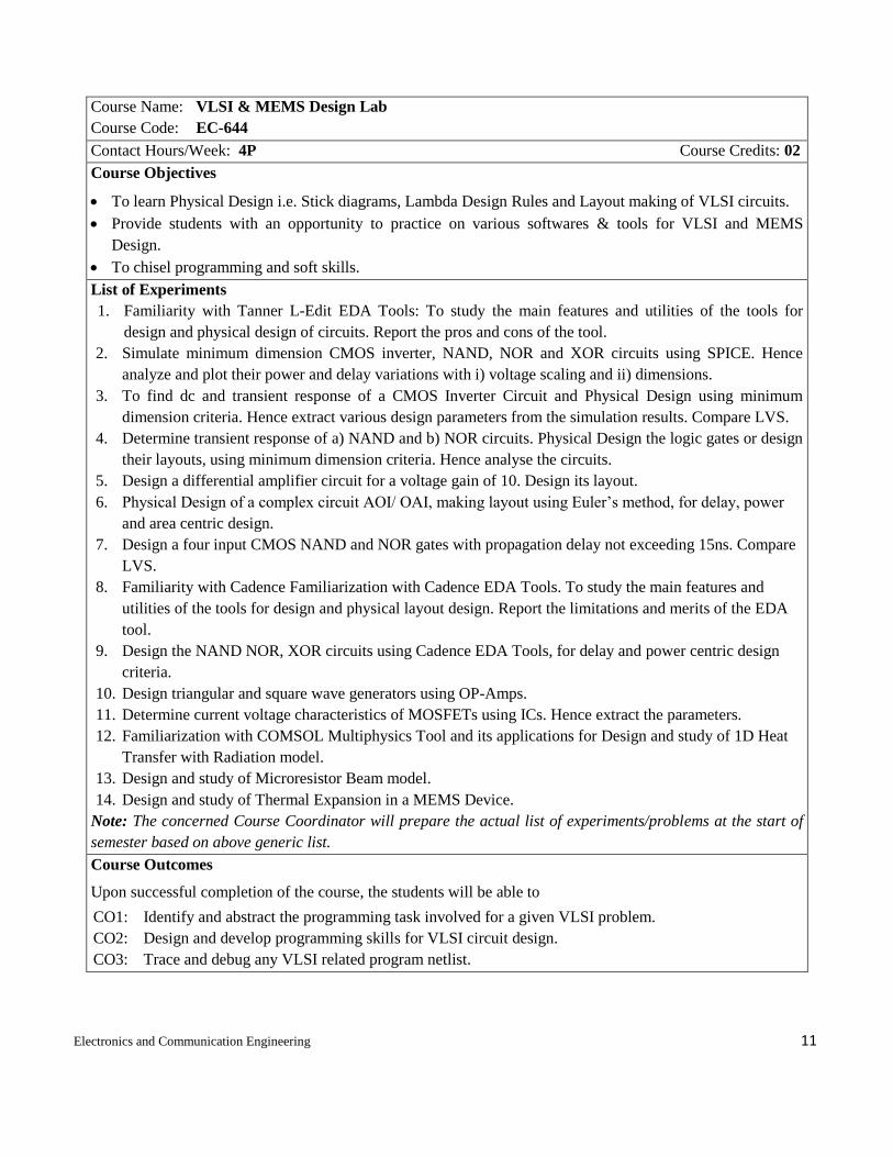
Course Name: VLSI & MEMS Design Lab
Course Code: EC-644
Contact Hours/Week: 4P Course Credits: 02
Course Objectives
To learn Physical Design i.e. Stick diagrams, Lambda Design Rules and Layout making of VLSI circuits.
Provide students with an opportunity to practice on various softwares & tools for VLSI and MEMS
Design.
To chisel programming and soft skills.
List of Experiments
1. Familiarity with Tanner L-Edit EDA Tools: To study the main features and utilities of the tools for
design and physical design of circuits. Report the pros and cons of the tool.
2. Simulate minimum dimension CMOS inverter, NAND, NOR and XOR circuits using SPICE. Hence
analyze and plot their power and delay variations with i) voltage scaling and ii) dimensions.
3. To find dc and transient response of a CMOS Inverter Circuit and Physical Design using minimum
dimension criteria. Hence extract various design parameters from the simulation results. Compare LVS.
4. Determine transient response of a) NAND and b) NOR circuits. Physical Design the logic gates or design
their layouts, using minimum dimension criteria. Hence analyse the circuits.
5. Design a differential amplifier circuit for a voltage gain of 10. Design its layout.
6. Physical Design of a complex circuit AOI/ OAI, making layout using Euler’s method, for delay, power
and area centric design.
7. Design a four input CMOS NAND and NOR gates with propagation delay not exceeding 15ns. Compare
LVS.
8. Familiarity with Cadence Familiarization with Cadence EDA Tools. To study the main features and
utilities of the tools for design and physical layout design. Report the limitations and merits of the EDA
tool.
9. Design the NAND NOR, XOR circuits using Cadence EDA Tools, for delay and power centric design
criteria.
10. Design triangular and square wave generators using OP-Amps.
11. Determine current voltage characteristics of MOSFETs using ICs. Hence extract the parameters.
12. Familiarization with COMSOL Multiphysics Tool and its applications for Design and study of 1D Heat
Transfer with Radiation model.
13. Design and study of Microresistor Beam model.
14. Design and study of Thermal Expansion in a MEMS Device.
Note: The concerned Course Coordinator will prepare the actual list of experiments/problems at the start of
semester based on above generic list.
Course Outcomes
Upon successful completion of the course, the students will be able to
CO1: Identify and abstract the programming task involved for a given VLSI problem.
CO2: Design and develop programming skills for VLSI circuit design.
CO3: Trace and debug any VLSI related program netlist.
Electronics and Communication Engineering 12
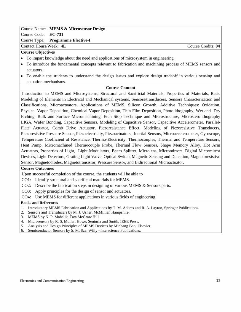
Course Name: MEMS & Microsensor Design
Course Code: EC-731
Course Type: Programme Elective-I
Contact Hours/Week: 4L Course Credits: 04
Course Objectives
To impart knowledge about the need and applications of microsystem in engineering.
To introduce the fundamental concepts relevant to fabrication and machining process of MEMS sensors and
actuators.
To enable the students to understand the design issues and explore design tradeoff in various sensing and
actuation mechanisms.
Course Content
Introduction to MEMS and Microsystems, Structural and Sacrificial Materials, Properties of Materials, Basic
Modeling of Elements in Electrical and Mechanical systems, Sensors/transducers, Sensors Characterization and
Classifications, Microactuators, Applications of MEMS, Silicon Growth, Additive Techniques: Oxidation,
Physical Vapor Deposition, Chemical Vapor Deposition, Thin Film Deposition, Photolithography, Wet and Dry
Etching, Bulk and Surface Micromachining, Etch Stop Technique and Microstructure, Microsterolithography
LIGA, Wafer Bonding, Capacitive Sensors, Modeling of Capacitive Sensor, Capacitive Accelerometer, Parallel-
Plate Actuator, Comb Drive Actuator, Piezoresistance Effect, Modeling of Piezoresistive Transducers,
Piezoresistive Pressure Sensor, Piezoelectricity, Piezoactuators, Inertial Sensors, Microaccelerometer, Gyroscope,
Temperature Coefficient of Resistance, Thermo-Electricity, Thermocouples, Thermal and Temperature Sensors,
Heat Pump, Micromachined Thermocouple Probe, Thermal Flow Sensors, Shape Memory Alloy, Hot Arm
Actuators, Properties of Light, Light Modulators, Beam Splitter, Microlens, Micromirrors, Digital Micromirror
Devices, Light Detectors, Grating Light Valve, Optical Switch, Magnetic Sensing and Detection, Magnetoresistive
Sensor, Magnetodiodes, Magnetotransistor, Pressure Sensor, and Bidirectional Microactuator.
Course Outcomes
Upon successful completion of the course, the students will be able to
CO1: Identify structural and sacrificial materials for MEMS.
CO2: Describe the fabrication steps in designing of various MEMS & Sensors parts.
CO3: Apply principles for the design of sensor and actuators.
CO4: Use MEMS for different applications in various fields of engineering.
Books and References
1. Introductory MEMS Fabrication and Applications by T. M. Adams and R. A. Layton, Springer Publications.
2. Sensors and Transducers by M. J. Usher, McMillian Hampshire.
3. MEMS by N. P. Mahalik, Tata McGraw Hill.
4. Microsensors by R. S. Muller, Howe, Senturia and Smith, IEEE Press.
5. Analysis and Design Principles of MEMS Devices by Minhang Bao, Elsevier.
6. Semiconductor Sensors by S. M. Sze, Willy –Interscience Publications.
Electronics and Communication Engineering 13
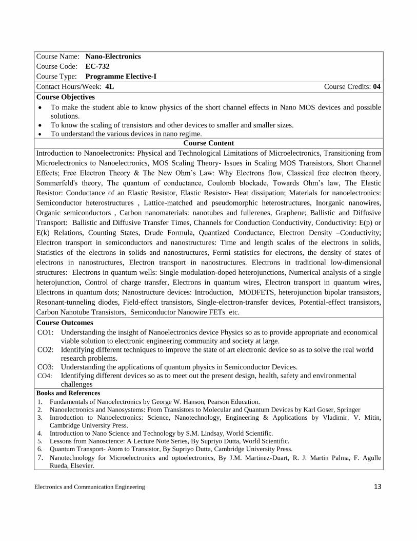
Course Name: Nano-Electronics
Course Code: EC-732
Course Type: Programme Elective-I
Contact Hours/Week: 4L Course Credits: 04
Course Objectives
To make the student able to know physics of the short channel effects in Nano MOS devices and possible
solutions.
To know the scaling of transistors and other devices to smaller and smaller sizes.
To understand the various devices in nano regime.
Course Content
Introduction to Nanoelectronics: Physical and Technological Limitations of Microelectronics, Transitioning from
Microelectronics to Nanoelectronics, MOS Scaling Theory- Issues in Scaling MOS Transistors, Short Channel
Effects; Free Electron Theory & The New Ohm’s Law: Why Electrons flow, Classical free electron theory,
Sommerfeld's theory, The quantum of conductance, Coulomb blockade, Towards Ohm’s law, The Elastic
Resistor: Conductance of an Elastic Resistor, Elastic Resistor- Heat dissipation; Materials for nanoelectronics:
Semiconductor heterostructures , Lattice-matched and pseudomorphic heterostructures, Inorganic nanowires,
Organic semiconductors , Carbon nanomaterials: nanotubes and fullerenes, Graphene; Ballistic and Diffusive
Transport: Ballistic and Diffusive Transfer Times, Channels for Conduction Conductivity, Conductivity: E(p) or
E(k) Relations, Counting States, Drude Formula, Quantized Conductance, Electron Density –Conductivity;
Electron transport in semiconductors and nanostructures: Time and length scales of the electrons in solids,
Statistics of the electrons in solids and nanostructures, Fermi statistics for electrons, the density of states of
electrons in nanostructures, Electron transport in nanostructures. Electrons in traditional low-dimensional
structures: Electrons in quantum wells: Single modulation-doped heterojunctions, Numerical analysis of a single
heterojunction, Control of charge transfer, Electrons in quantum wires, Electron transport in quantum wires,
Electrons in quantum dots; Nanostructure devices: Introduction, MODFETS, heterojunction bipolar transistors,
Resonant-tunneling diodes, Field-effect transistors, Single-electron-transfer devices, Potential-effect transistors,
Carbon Nanotube Transistors, Semiconductor Nanowire FETs etc.
Course Outcomes
CO1: Understanding the insight of Nanoelectronics device Physics so as to provide appropriate and economical
viable solution to electronic engineering community and society at large.
CO2: Identifying different techniques to improve the state of art electronic device so as to solve the real world
research problems.
CO3: Understanding the applications of quantum physics in Semiconductor Devices.
CO4: Identifying different devices so as to meet out the present design, health, safety and environmental
challenges
Books and References
1. Fundamentals of Nanoelectronics by George W. Hanson, Pearson Education.
2. Nanoelectronics and Nanosystems: From Transistors to Molecular and Quantum Devices by Karl Goser, Springer
3. Introduction to Nanoelectronics: Science, Nanotechnology, Engineering & Applications by Vladimir. V. Mitin,
Cambridge University Press.
4. Introduction to Nano Science and Technology by S.M. Lindsay, World Scientific.
5. Lessons from Nanoscience: A Lecture Note Series, By Supriyo Dutta, World Scientific.
6. Quantum Transport- Atom to Transistor, By Supriyo Dutta, Cambridge University Press.
7. Nanotechnology for Microelectronics and optoelectronics, By J.M. Martinez-Duart, R. J. Martin Palma, F. Agulle
Rueda, Elsevier.
Electronics and Communication Engineering 14
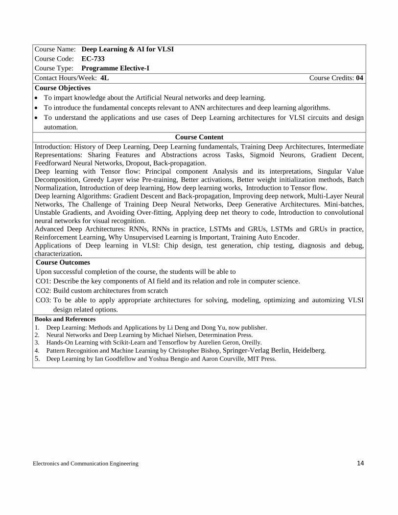
Course Name: Deep Learning & AI for VLSI
Course Code: EC-733
Course Type: Programme Elective-I
Contact Hours/Week: 4L Course Credits: 04
Course Objectives
To impart knowledge about the Artificial Neural networks and deep learning.
To introduce the fundamental concepts relevant to ANN architectures and deep learning algorithms.
To understand the applications and use cases of Deep Learning architectures for VLSI circuits and design
automation.
Course Content
Introduction: History of Deep Learning, Deep Learning fundamentals, Training Deep Architectures, Intermediate
Representations: Sharing Features and Abstractions across Tasks, Sigmoid Neurons, Gradient Decent,
Feedforward Neural Networks, Dropout, Back-propagation.
Deep learning with Tensor flow: Principal component Analysis and its interpretations, Singular Value
Decomposition, Greedy Layer wise Pre-training, Better activations, Better weight initialization methods, Batch
Normalization, Introduction of deep learning, How deep learning works, Introduction to Tensor flow.
Deep learning Algorithms: Gradient Descent and Back-propagation, Improving deep network, Multi-Layer Neural
Networks, The Challenge of Training Deep Neural Networks, Deep Generative Architectures. Mini-batches,
Unstable Gradients, and Avoiding Over-fitting, Applying deep net theory to code, Introduction to convolutional
neural networks for visual recognition.
Advanced Deep Architectures: RNNs, RNNs in practice, LSTMs and GRUs, LSTMs and GRUs in practice,
Reinforcement Learning, Why Unsupervised Learning is Important, Training Auto Encoder.
Applications of Deep learning in VLSI: Chip design, test generation, chip testing, diagnosis and debug,
characterization.
Course Outcomes
Upon successful completion of the course, the students will be able to
CO1: Describe the key components of AI field and its relation and role in computer science.
CO2: Build custom architectures from scratch
CO3: To be able to apply appropriate architectures for solving, modeling, optimizing and automizing VLSI
design related options.
Books and References
1. Deep Learning: Methods and Applications by Li Deng and Dong Yu, now publisher.
2. Neural Networks and Deep Learning by Michael Nielsen, Determination Press.
3. Hands-On Learning with Scikit-Learn and Tensorflow by Aurelien Geron, Oreilly.
4. Pattern Recognition and Machine Learning by Christopher Bishop, Springer-Verlag Berlin, Heidelberg.
5. Deep Learning by Ian Goodfellow and Yoshua Bengio and Aaron Courville, MIT Press.
Electronics and Communication Engineering 15
Course Name: Deep Submicron VLSI Design Issues
Course Code: EC-734
Course Type: Programme Elective-I
Contact Hours/Week: 4L Course Credits: 04
Course Objectives
To teach fundamentals of deep submicron (DSM) technologies in VLSI.
To give an insight into the various non-ideal effects in DSM.
To provide remedial measures for various issues in DSM VLSI design.
Course Content
Evolution of the structure of MOSFETs, the structure of deep-submicron MOSFETs (0.25-μm to 0.13-μm),
compare to the structure of the conventional MOSFETs (2.0-μm to 0.5-μm), evolution of the MOSFET gate stack
and contact structure, gate dielectric materials in deep-submicron MOSFETs, doping-concentration profiles of the
MOSFET channel, evolution of the drain structure of MOSFETs. Deep-submicron CMOS structures, Substrate
issues for deep-submicron CMOS, well formation in deep-submicron CMOS, dual-doped poly in deep-submicron
CMOS, shallow trench isolation for deep-submicron CMOS, silicon-on-insulator (SOI) technology. 300-mm
Silicon Wafers, 300-mm silicon crystal growth, grown-in silicon defects, formation of crystal-originated-particles
(cops), the oxygen-stacking-fault ring (OSF-ring), mitigating effects of cops by use of post-crystal-growth
annealing, high pull speed silicon, from ingot to finished wafer, slicing, etching, & polishing, specifications of
silicon wafers for VLSI. Gate Dielectrics, Thin Gate Oxides, required characteristics of gate dielectrics for deep-
submicron MOSFETs, the structure of thermally grown SiO2 and the properties of the Si/SiO2 interface, Dielectric
breakdown in silicon dioxide films trapped in SiO2, Leakage currents in SiO2 films (tunneling phenomena),
Manufacturing thin gate oxides, High-k dielectrics and low-k dielectrics. The Structure of Deep-Submicron
MOSFETs, well-formation in deep-submicron CMOS, Super-steep retrograde channel (SSR) profiles Source/drain
engineering in deep-submicron CMOS, Anti-punch-through structures in deep-submicron CMOS. Advanced
Lithography and Chemical Mechanical Polishing (CMP) Deep-submicron resists, Chemically-amplified deep-UV
resists for optical lithography, chemically-amplified deep-UV resists for optical lithography, anti-reflective
coating (arcs), photoresist processing systems. Optics and hardware, Excimer laser deep-UV light sources,
exposure tools for DUV lithography, resolution enhancement technologies (RETS), mask error factor (MEF or
MEEF), non-optical (or next generation) lithographic technologies (NGL) Mechanisms of CMP, CMP equipment,
cleaning issues in CMP, miscellaneous issues in CMP. Shallow Trench Isolation (STI), Shallow trench isolation
for CMOS, details of the process flow to form a baseline shallow-trench-isolation (STI) structure, issues and
characteristics of MOSFETs fabricated with STI.
Course Outcomes
CO1: Comprehend the insight of deep submicron (DSM) VLSI design.
CO2: Identify the non-ideal issues and remedial solutions for these.
CO3: Assess and analyse the performance of DSM VLSI designs.
Books and References
1. Silicon Processing for the VLSI Era: Deep-Submicron Process Technology by Stanley Wolf, Lattice Pr.
2. Deep-Submicron CMOS ICs: From Basics to ASICs by Harry Veendrick, Kluwer Academic.
Electronics and Communication Engineering 16
Course Name: Characterization of Semiconductor Materials & Devices
Course Code: EC-735
Course Type: Programme Elective-II
Contact Hours/Week: 4L Course Credits: 04
Course Objectives
To impart knowledge about properties of various semiconductor materials.
To introduce the semiconductor physics behind the materials
To enable the students to understand the design of semiconductor devices using electronic materials
To understand how various semiconductor devices behave and how to optimize them
Course Content
Introduction to Electronic Materials, Crystal structure, Band theory, Carrier concentration at thermal equilibrium,
Density of states, Fermi energy, Ionization impurity in semiconductors, Quantum aspect of semiconductors,
Carrier transport, Random motion, Drift and diffusion, Excess carriers Injection level, Lifetime, Direct and
indirect semiconductors, Measurement of Semiconductor Properties, Procedure for analyzing semiconductor
devices, Basic equations and approximations, Characteristics and energy band diagrams of PN Junction diodes,
Schottky barrier diode, Bipolar Junction Transistor, Field Effect Transistors, Optoelectronic Devices; LED,PIN
Photodetector, Semiconductor LASER
Course Outcomes
Upon successful completion of the course, the students will be able to
CO1: Identify various Materials useful in designing Semiconductor Devices.
CO2: Understand the semiconductor physics of the material.
CO3: Apply different material characteristics for designing of Semiconductor devices.
CO4: Understand the theoretical concepts of various semiconductor devices and their applications.
Books and References
1. Physics of Semiconductor Devices by S.M. Sze, Wiley Publication.
2. Semiconductor Materials and Devices by M.S. Tyagi, Wiley Publication.
3. Solid State Electronics Devices by B.G. Streetman, Prentice Hall.
4. Semiconductor Devices by Kanaan Kano, Prentice Hall.
Electronics and Communication Engineering 17
Course Name: CMOS RF Circuit Design
Course Code: EC-736
Course Type: Programme Elective-II
Contact Hours/Week: 4L Course Credits: 04
Course Objectives
To impart knowledge about the RF circuit design and Wireless Technology.
To introduce the fundamental concepts of RF modulation along with RF testing.
To enable the students to understand the behavior of BJT and MOSFET at RF frequencies.
Course Content
Introduction to RF design and Wireless Technology: Design and applications, Complexity and choice of
Technology, Basic concepts in RF design, Nonlinearly and time Variance, Inter-symbol interference, Random
processes and noise, Sensitivity and dynamic range, Conversion of gains and distortion, RF Modulation: Analog
and digital modulation of RF circuits, Comparison of various techniques for power efficiency, Coherent and non-
coherent detection, Mobile RF communication and basics of Multiple Access techniques, Receiver and
Transmitter architectures, Direct conversion and two-step transmitters, RF Testing: RF testing for heterodyne,
Homodyne, Image reject, Direct IF and sub sampled receivers, BJT and MOSFET Behavior at RF Frequencies:
BJT and MOSFET behavior at RF frequencies, Modeling of the transistors and SPICE model, Noise performance
and limitations of devices, Integrated parasitic elements at high frequencies and their monolithic implementation,
RF Circuits Design: Overview of RF Filter design, Active RF components & modeling, Matching and Biasing
Networks. Basic blocks in RF systems and their VLSI implementation, Low noise Amplifier design in various
technologies, Design of Mixers at GHz frequency range, Various mixers working and implementation.
Oscillators- Basic topologies VCO and definition of phase noise, Noise power and trade off. Resonator VCO
designs, Quadrature and single sideband generators. Radio frequency Synthesizers- PLLS, Various RF synthesizer
architectures and frequency dividers, Power Amplifier design, Liberalization techniques, Design issues in
integrated RF filters.
Course Outcomes
Upon successful completion of the course, the students will be able to
CO1: Understand the basic concepts of RF design, behavior of passive components and RF modulation.
CO2: Realize the behavior of BJT and MOSFET parameters at RF range.
CO3: Design high frequency amplifiers.
CO4: Explain the biasing and referencing in devices at RF range.
CO5: Design RF circuits and explain RF synthesizers.
Books and References
1. Design of CMOS RF Integrated Circuits by Thomas H. Lee, Cambridge University press.
2. RF Microelectronics by Razavi, PHI.
3. CMOS Circuit Design, layout and Simulation by R. Jacob Baker, H.W. Li, D.E. Boyce, PHI.
4. Mixed Analog and Digital Devices and Technology by Y.P. Tsividis, TMH.
Electronics and Communication Engineering 18
Course Name: VLSI Test & Testability
Course Code: EC-737
Course Type: Programme Elective-II
Contact Hours/Week: 4L Course Credits: 04
Course Objectives
To impart knowledge about the basics of testing techniques for VLSI circuits and Test Economics
To introduce the fundamental concepts of Design for Testability.
To enable the students to generate the test patterns.
Course Content
Basics of Testing and Fault Modeling: Introduction to Testing, Test process and ATE, Faults in digital circuits,
Modeling of faults, Logical Fault Models, Fault detection, Fault location, Fault dominance, Logic Simulation,
Types of simulation, Delay models, Gate level Event-driven simulation.
Test Generation for Combinational and Sequential Circuits: Logic simulation and fault simulation, Testability
measures, Test generation for combinational logic circuits, Testable combinational logic circuit design, Test
generation for sequential circuits, design of testable sequential circuits.
Design for Testability Design for Testability: Ad-hoc design, Generic scan based design, Classical scan based
design – System level DFT approaches, Memory test.
Self-Test and Test Algorithms Built-In Self-Test: Test pattern generation for BIST, Circular BIST, BIST
Architectures, Testable Memory Design, Test algorithms, Test generation for Embedded RAMs, Logic BIST and
EDT, Boundary Scan, System test and core test.
Fault Diagnosis Logic Level Diagnosis: Diagnosis by UUT reduction, Fault Diagnosis for Combinational Circuits,
Self-checking design, System Level Diagnosis.
Course Outcomes
Upon successful completion of the course, the students will be able to
CO1: Apply the concepts in testing which can help them design a better yield in IC design.
CO2: Tackle the problems associated with testing of integrated circuits at earlier design levels so as to
significantly reduce the testing costs.
CO3: Identify the design for testability methods for combinational & sequential CMOS circuits
Books and References
1. Digital Systems and Testable Design by M. Abramovici, M.A. Breuer and A.D. Friedman, Jaico Publishing House.
2. Essentials of Electronic Testing for Digital, Memory and Mixed-Signal VLSI Circuits by M.L. Bushnell and V.D. Agrawal,
Kluwer Academic Publishers.
3. Digital Circuit Testing and Testability by P.K. Lala, Academic Press.
4. Design Test for Digital IC's and Embedded Core Systems by A.L. Crouch, Prentice Hall International.
Electronics and Communication Engineering 19
Course Name: VLSI Interconnects
Course Code: EC-738
Course Type: Programme Elective-II
Contact Hours/Week: 4L Course Credits: 04
Course Objectives
To impart knowledge about the importance of electrical on-chip interconnects in modern VLSI circuits
To introduce the various equivalent circuit models of interconnects and their comparison
To understand the short-channel model of CMOS repeater driving interconnect and its analysis
To enable the students to understand the advanced interconnect techniques
Course Content
Interconnect Parameters, resistance, inductance, and capacitance, RC Delays, lumped RC Model, distributed
RC Model, transmission line model, SPICE wire models, gate and interconnect delay, CMOS repeater, static
and dynamic behavior, switching threshold, noise margins, computing the capacitances, propagation delay,
first order analysis, propagation delay from a design perspective. Driving interconnects for optimum speed
and power, short channel model of CMOS repeater, transient analysis of an RC loaded CMOS repeater, delay
analysis, analytical power expressions: dynamic power, short circuit power, resistive power dissipation,
CMOS repeater insertion: analytical expressions for delay and power of a repeater chain driving an RC load.
Advanced interconnect techniques: reduced-swing circuits, current mode transmission techniques. Crosstalk,
theoretical basis and circuit level modeling of crosstalk, energy dissipation due to crosstalk, model for energy
calculation of two coupled lines, contribution of driver and interconnect to dissipated energy, crosstalk effects
in logic VLSI circuits, static circuits, dynamic circuits and various remedies.
Course Outcomes
Upon successful completion of the course, the students will be able to
CO1: Develop the ability to analyze and design electrical interconnect using equivalent circuit models.
CO2: Understand the use of CMOS repeater to predict delay and power in interconnects.
CO3: Describe the design trade-offs in driver-interconnect-load system.
CO4: Design crosstalk and delay aware repeater driven interconnect system using advanced signaling
techniques.
Books and References
1. 1. Analysis and Design of Digital Integrated Circuits – A Design Perspective by Jan M. Rabaey, Tata Mc-Graw Hill.
2. Interconnection Noise in VLSI Circuits by F. Moll and M. Roca, Kluwer Academic Publishers.
3. Introduction to VLSI Circuits and Systems by J. P. Uymera, Wiley Student Edition.
4. CMOS Digital Integrated Circuits – Analysis and Design by S. M. Kang and L. Yusuf, Tata Mc-Graw Hill.
Electronics and Communication Engineering 20
Course Name: Low Power VLSI Design
Course Code: EC-739
Course Type: Programme Elective-III
Contact Hours/Week: 4L Course Credits: 04
Course Objectives
To impart knowledge about the dominant sources of power dissipation in VLSI circuits.
To introduce the fundamental concepts for optimization of power at all design levels: technology, circuit, logic,
and architectural level.
To enable the students to aware of power estimation by various means.
Course Content
Need for Low Power VLSI Chips, Sources of Power Dissipation in CMOS Devices, Dynamic Power Dissipation
in CMOS, Static Power Dissipation, Low Power Figure of Merits, Impact of Technology Scaling, Device
Innovation and Channel Engineering, Simulation Power Analysis- SPICE Circuit Simulators, Gate Level Logic
Simulation, Capacitive
Power Estimation, Static State Power, Gate Level Capacitance Estimation, Architecture Level Analysis, Data
Correlation Analysis in DSP Systems. Monte Carlo Simulation, Probabilistic Power Analysis- Random Logic
Signals, Probability and Frequency, Probabilistic Power Analysis Techniques, Low Power Circuit and Logic
Design, Transistor and Gate Sizing, Multi Stage Logic Design, Reduced Voltage Swing, Circuit Techniques for
Leakage Power Reduction, Transistor Stacking, Supply Voltage Scaling Techniques, DTCMOS, MTCMOS,
Network Restructure and Reorganization, Flip Flops and Latches Design, Gated Clock Flip Flop, Double Edge
Triggered Flip Flop, Low Power Digital Cell Library, Gate Reorganization, Signal Gating, Logic Encoding, State
Machine Encoding, Pre-Computation Logic, Adiabatic Logic, Low Power Arithmetic Components, Low Power
Architecture and Systems, Power and Performance Management , Low Power Stand By Modes, Switching
Activity Reduction, Parallel and Pipelining Architecture with Voltage Reduction, Flow Graph Transformation,
Architectural Trade-Offs for Power, Power Dissipation In Clock Distribution, Single Driver Vs Distributed
Buffers, Zero Skew Vs Tolerable Skew, and Clock Distribution Network.
Course Outcomes
Upon successful completion of the course, the students will be able to
CO1: Identify sources of power dissipation in VLSI systems.
CO2: Analyze various techniques for dynamic and leakage power reduction at various level of abstraction.
CO3: Design arithmetic circuits, latches and flip flops with different logic styles.
CO4: Understand the concepts of probability and random logic signals for estimation of capacitance and power
Dissipation. Books and References
1. Practical Low Power Digital VLSI Design by Gary K. Yeap, Kluwer Academic Press.
2. Low-Power CMOS VLSI Circuit Design by Kaushik Roy, Sharat Prasad, Wiley.
3. Low Power VLSI CMOS Circuit Design by A. Bellamour, and M. I. Elmasri, Kluwer Academic Press.
4. Low Power Design Methodologies by Rabaey and Pedram, Kluwer Academic Press.
5. Low-Voltage Low-Power VLSI subsystems by Kait-Seng Yeo and Kaushik Roy, Tata McGraw-Hill.
6. Low Power Digital CMOS Design by Anantha P. Chandrakasan and Robert W. Brodersen, Kluwer Academic Press.
Electronics and Communication Engineering 21
Course Name: Advanced Semiconductor Devices
Course Code: EC-740
Course Type: Programme Elective-III
Contact Hours/Week: 4L Course Credits: 04
Course Objectives
To teach about various advanced semiconductor devices.
To build upon the theoretical and mathematical models for working and behavior of the advanced
semiconductor devices.
To understand and practice designing of VLSI circuits with advanced devices.
Course Content
Review of semiconductors fundamentals, semiconductor materials and their properties, band structure
modification by alloys, carrier transport in semiconductors, scattering, defects, phonons, mobility, excess carriers
in semiconductor, reverse recovery time. Junctions and interfaces, description of p-n junction, action, abrupt
junction, example of an abrupt junction, linearly graded Junction. Ideal diode model, real diodes, temperature
dependence of current-voltage (I-V) characteristics, high level injection effects, example of diodes. Description of
breakdown mechanism, Zener and Avalanche breakdown in p-n junctions. Majority carrier diodes, Tunnel diode,
backward diode, Schottky barrier diode, Ohmic contacts, heterojunctions. Microwave diodes, varactor diode, p-i-n
Diode, IMPATT diode, TRAPATT diode, BARITT diode, transferred electron devices. Optoelectronic devices
&nano-electronics, solar cell, photo detectors, light emitting diodes, semiconductor lasers. Nano devices, material
and classification, issues in scaling MOS transistors, transport in nano MOSFET, carbon nanotubes (CNTs). Metal
semiconductor field effect transistors, basic types of MESFETs, models for I-V characteristics of short channel
MESFETs, high frequency performance, MESFETs structures. MOS transistors and charge coupled devices, basic
structures and the operating principle, I-V characteristics, short- channel effects, charge coupled devices.
Course Outcomes
Upon successful completion of the course, the students will be able to
CO1: Identify the conventional and new state of the art semiconductor devices.
CO2: Apply the theoretical and mathematical models of the advanced devices for usage in electronic design.
CO3: Assess and analyse the performance of advanced semiconductor devices and circuits.
Books and References
1. Advanced Theory of Semiconductor Devices by Karl Hess, Wiley-IEEE Press.
2. Physics of Semiconductors and their Heterostructures by Jasprit Singh, McGraw-Hill Education.
3. Advanced Semiconductor Fundamentals by Robert F. Pierret, Prentice Hall.
4. Fundamentals of Modern VLSI Devices by Y. Taur and T. Ning, Cambridge University Press.
Electronics and Communication Engineering 22
Course Name: Verification of VLSI Circuits
Course Code: EC-741
Course Type: Programme Elective-III
Contact Hours/Week: 4L Course Credits: 04
Course Objectives
To impart knowledge about the verification of VLSI circuits.
To introduce the concepts of Verification techniques, UML and considerations
To demonstrate the hardware acceleration and emulation techniques
Course Content
Design and Verification Languages Stephen A. Edwards: Introduction, History, Design Languages, Verification
Languages.
Digital Simulation: Introduction, Event-vs Process-Oriented Simulation, Logic Simulation Methods and
Algorithms, Impact of Languages on Logic simulation, Logic Simulation Techniques, Impact of HVLs on
simulation, Summary.
Using Transactional-Level Models in a SoC Design Flow: Introduction, Overview of the System-to-RTL Design
Flow, TLM —View for the Design Flow, TLM Modeling Application Programming Interface, Example of a
Multimedia Platform, Design Flow Automation, Conclusion.
Hardware Acceleration and Emulation: Introduction, Emulator Architecture Overview, Design Modeling,
Debugging, Use Models, The Value of In-Circuit Emulation, Considerations for Successful Emulation, Summary.
Formal Property Verification: Introduction, Formal Property Verification Methods and Technologies, Software
Formal Verification, Summary.
Course Outcomes
Upon successful completion of the course, the students will be able to
CO1: Able to verify digital circuits for design errors.
CO2: Understand the constraints and corner cases.
CO3: Utilize techniques and technology for efficient circuit verification.
Books and References
1. EDA for IC System Design, Verification, and Testing by Louis Scheffer, Luciano Lavagno, and Grant Martin.
2. Verification Techniques for System-Level Design by M. Fujita, I. Ghosh, and M. Prasad, , Morgan Kaufmann.
3. Formal Verification: An Essential Toolkit for Modern VLSI Design by Erik Seligman, Morgan Kaufmann.
Electronics and Communication Engineering 23
Course Name: Embedded System Design
Course Code: EC-742
Course Type: Programme Elective-III
Contact Hours/Week: 4L Course Credits: 04
Course Objectives
To familiarize the students with the basic design concepts for designing embedded systems
To be able to design the embedded system for any use case
Course Content
Typical Embedded System: Core of the Embedded System, Memory, Sensors and Actuators, Communication
Interface, Embedded Firmware, Other System Components.
Characteristics and Quality Attributes of Embedded Systems: Hardware Software Co-Design and Program
Modeling: Fundamental Issues in Hardware Software Co-Design, Computational Models in Embedded Design,
Introduction to Unified Modeling Language, Hardware Software Trade-offs.
Embedded Hardware Design and Development: EDA Tools, How to Use EDA Tool, Schematic Design – Place
wire, Bus , port, junction, creating part numbers, Design Rules check, Bill of materials, Netlist creation , PCB
Layout Design – Building blocks, Component placement, PCB track routing.
ARM -32 bit Microcontroller family: Architecture of ARM Cortex M3 –General Purpose Registers, Stack Pointer,
Link Register, Program Counter, Special Register. Nested Vector Interrupt Controller. Interrupt behavior of ARM
Cortex M3. Exceptions Programming. Advanced Programming Features. Memory Protection. Debug Architecture.
Embedded Firmware Design and Development, Design Approaches, Embedded Firmware Development
Languages.
Real-Time Operating System (RTOS) based Embedded System Design: Operating System Basics, Types of OS,
Tasks, Process and Threads, Multiprocessing and Multitasking, Task Scheduling, Threads, Processes and
Scheduling: Putting them altogether, Task Communication, Task Synchronization, Device Drivers, How to
Choose an RTOS, Integrated Development Environment (IDE), Types of Files Generated on Cross compilation,
Disassembler/ELD compiler, Simulators, Emulators and Debugging, Target Hardware Debugging, Boundary
Scan.
Course Outcomes
Upon successful completion of the course, the students will be able to
CO1: Define a real life problem in terms of technical specification of relevant embedded system.
CO2: Understand the processor and memory and to learn different types of I/O Devices, timer and counting
devices.
CO3: Design the embedded system as per the specification and can understand the importance of Hardware-
Software Co-design in an Embedded System
Books and References
1. Introduction to Embedded Systems by Shibu K V, Tata McGraw Hill Education Private Limited.
2. The Definitive Guide to the ARM Cortex-M3 by Joseph Yiu, Newnes, (Elsevier).
3. Embedded Systems – A contemporary Design Tool by James K Peckol, John Wiley.
4. Specification and Design of Embedded Systems by D. Gajski, F. Vahid, S. Narayan, and J. Gong., Prentice Hall.
5. Hardware Software Co-design: Principles and Practice by Jorgan Syaunstrup and W. Wolf., Kluwer Academic
Publishers.
Electronics and Communication Engineering 24
Course Name: SoC and FPGA Based Design
Course Code: EC-743
Course Type: Programme Elective-IV
Contact Hours/Week: 4L Course Credits: 04
Course objectives
To give the student an understanding of issues and tools related to FPGA design and implementation.
To give the student an understanding of basics of system on chip and platform based design.
To impart knowledge about the system-level and SoC design methodologies and tools.
Course Content
Types of ASICs: Types of ASICs, VLSI Design flow, Programmable ASICs, Antifuse, SRAM, EPROM,
EEPROM based ASICs. Programmable ASIC logic cells and I/O cells. Programmable interconnects. Latest
Version, FPGAs and CPLDs and Soft-core processors.
Design Specification and Resource Scoping: Trade off issues at System Level: Optimization with regard to speed,
area and power, asynchronous and low power system design. ASIC physical design issues, System Partitioning,
Power Dissipation, Partitioning Methods.
SoC Block-Based Design: System-On-Chip Design, SoC Design Flow, Platform-based and IP based SoC Designs,
Basic Concepts of Bus-Based Communication Architectures, On-Chip Communication Architecture Standards,
Low-Power SoC Design, Performance Evaluation Methods for Multiprocessor System-on-Chip Design.
FPGA Design Environment: Introduction, Scripting Environment, Interaction with Version Control Software, A
Regression Test System, Common Tools in the FPGA Design Environment, Challenges that FPGAs Create for
Board Design, Engineering Roles and Responsibilities, FPGA Engineers, Design Flows for Creating the FPGA
Pinout, Board Design Check List for a Successful FPGA Pin-Out.
Power Analysis and RTL Design: Introduction, Power Basic, Key Factors in Accurate Power Estimation, Power
Estimation Early in the Design Cycle, Simulation Based Power Estimation, Best Practices for Power Estimation,
Recommendations for Engineers with an ASIC Design Background, Writing Effective HDL, Analyzing the RTL
Design.
The Hardware/Software considerations: Introduction, Software Interface, Definition of Register Address Map,
Use of the Register Address Map, Hardware/Software Co-Design and Verification, High performance algorithms
for ASICS/ SoCs as case studies – Canonic Signed Digit Arithmetic, Distributed Arithmetic.
Course Outcomes
Upon successful completion of the course, the students will be able to
CO1: Demonstrate VLSI tool-flow and appreciate FPGA architecture
CO2: Understand the basics of system on chip and on chip communication architectures.
CO3: Understand the issues involved in ASIC design, including technology choice, design management, tool-
flow.
Books and References
1. Embedded System Design: Modeling, Synthesis and Verification by D. Gajski, S. Abdi, A. Gerstlauer, G. Schirner,
Springer.
2. Synthesis and Optimization of Digital Circuits by G. De Micheli, McGraw-Hill.
3. EDA for IC System Design, Verification, and Testing by Louis Scheffer, Luciano Lavagno, and Grant Martin.
4. Verilog Digital Computer Design by Mark Gordon Arnold.
Electronics and Communication Engineering 25
Course Name: Hardware Algorithms for VLSI
Course Code: EC-744
Course Type: Programme Elective-IV
Contact Hours/Week: 4L Course Credits: 04
Course Objectives
To impart knowledge about the computer arithmetic algorithms, including different techniques enabling
enhanced throughput and low power.
To understand algorithms techniques to hardware implementation of various arithmetic operations.
Course Content
Numbers and Arithmetic: Review of Number systems, their encoding and basic arithmetic operations, Class of
Fixed-Radix Number Systems, Unconventional fixed-point number systems, Representing Signed Numbers,
Negative-radix number Systems, Redundant Number Systems, Residue Number Systems.
Algorithms for Fast Addition: Basic Addition and Counting, Bit-serial and ripple-carry adders, Addition of a
constant: counters, Manchester carry chains and adders, Carry-Look-ahead Adders, Carry determination as prefix
computation, Alternative parallel prefix networks, VLSI implementation aspects, Variations in Fast Adders,
Simple carry-skip and Carry-select adders, Hybrid adder designs, Optimizations in fast adders, Multi-Operand
Addition, Wallace and Dadda trees, Parallel counters, Generalized parallel counters, Adding multiple signed
numbers.
High-Speed Multiplication: Basic Multiplication Schemes, Shift/add multiplication algorithms, Programmed
multiplication, Basic hardware multipliers, Multiplication of signed numbers, Multiplication by constants,
Preview of fast multipliers, High-Radix Multipliers, Modified Booth's recoding, Tree and Array Multipliers,
Variations in Multipliers, VLSI layout considerations.
Fast Division and Division Through Multiplication: Basic Division Schemes, Shift/subtract division algorithms,
Programmed division, Restoring hardware dividers, Non-restoring and signed division, Division by constants,
Preview of fast dividers, High-Radix Dividers, Variations in Dividers, Combined multiply/divide units, Division
by Convergence, Hardware implementation.
Real Arithmetic: Representing the Real Numbers, Floating-point arithmetic, The ANSI/IEEE floating point
standard, Exceptions and other features, Floating-point arithmetic operations, Rounding schemes, Logarithmic
number systems, Floating-point adders, Barrel-shifter design, Leading-zeros/ones counting, Floating-point
multipliers, Floating-point dividers, Arithmetic Errors and Error Control.
Implementation Topics: Computing algorithms, Exponentiation, Approximating functions, Merged arithmetic,
Arithmetic by Table Lookup, Tradeoffs in cost, speed, and accuracy. High-Throughput Arithmetic, Low-Power
Arithmetic, Fault-Tolerant Arithmetic, Emerging Trends, Impact of Hardware Technology.
Course Outcomes
Upon successful completion of the course, the students will be able to
CO1: Understand hardware implementation of various algorithms
CO2: Learn to apply tradeoffs and multiple implementations and architectures
CO3: Know the use cases of various algorithms and their considerations
Books and References
1. Computer Arithmetic: Algorithms and Hardware Design by Parhami, B., Oxford University Press.
2. Computer Arithmetic Algorithms by Koren, I., CRC Press.
3. Digital Arithmetic by Ercegovac, M. and Lang, T., Elsevier.
4. Verilog Digital Computer Design Algorithms into Hardware by Mark Gordon Arnold, Prentice Hall PTR.
Electronics and Communication Engineering 26
Course Name: Biomedical Electronics
Course Code: EC-745
Course Type: Programme Elective-IV
Contact Hours/Week: 4L Course Credits: 04
Course Objectives
To teach fundamentals of biomedical processes of human body.
To understand the theory and techniques to monitor biomedical process.
To provide an insight into use of the biomedical equipment for monitoring human body problems.
Course Content
Characteristics of Transducers and Electrodes for Biological Measurement, Introduction to human body, block
diagram, classification, characteristics, various physiological events and suitable transducer for their recording,
bioelectric potentials. Cardiac System, Cardiac musculature, Electro cardiography, ECG recording,
Phonocardiography, ECG lead system, Heart rate meter, vector cardiography, Defibrillators. Blood Pressure and
Blood Flow Measurement, Invasive and non-invasive methods of Blood pressure, Characteristics of blood flow
and heart sound, Cardiac output measurement, Plethysmography. Respiratory System, Mechanics of breathing,
Parameters of respiration, Respiratory system measurements, Respiratory therapy instruments. Instrumentation for
Measuring Nervous Function, EEG signal, frequency band classification, Lead systems, EEG recording, Clinical
applications of EEG signal, X-ray CT scan, MRI, PET. Recent Trends in Biomedical Engineering, Patient care
and monitoring, Non-invasive diagnostic instrumentation, Biotelemetry, Telemedicine, Prosthetic devices, Lie
detector test, Application of lasers and ultrasonic in biomedical field.
Course Outcomes
Upon successful completion of the course, the students will be able to
CO1: Identify the various biomedical processes and problems associated with human body.
CO2: Apply principles of electronics and instrumentation to cope up with biomedical processes.
CO3: Assess and analyse the performance of biomedical electronic devices and signal processing. Books and References
1. Introduction to Bio-medical Instrumentation by R.S. Khandpur, McGraw Hill Education.
2. Bio Medical Instrumentation by Cromwell, Prentice Hall India Learning Private Limited.
Electronics and Communication Engineering 27
Course Name: Digital Image Processing
Course Code: EC-746
Course Type: Programme Elective-IV
Contact Hours/Week: 4L Course Credits: 04
Course Objectives
To understand the basics of image formation and filtering in spatial and frequency domain.
To understand the concepts of image compression, image segmentation and morphological operation on image.
To understand the pattern recognition and Neural Network for pattern classification.
Course Content
Introduction: Steps in Digital Image Processing, Components of an Image Processing system, Applications.
Human Eye and Image Formation; Sampling and Quantization, Basic Relationship among pixels- neighbour,
connectivity, regions, boundaries, distance measures; Image Enhancement: Spatial Domain, Gray Level
transformations, Histogram, Arithmetic/Logical Operations, Spatial filtering, Smoothing & Sharpening Spatial
Filters; Frequency Domain- 2-D Fourier transform, Smoothing and Sharpening Frequency Domain Filtering;
Convolution and Correlation Theorems; Image Restoration: Inverse filtering, Wiener filtering; Wavelets- Discrete
and Continuous Wavelet Transform, Wavelet Transform in 2-D; Image Compression: Redundancies- Coding,
Interpixel, Psycho visual; Fidelity, Source and Channel Encoding, Elements of Information Theory; Loss Less and
Lossy Compression; Run length coding, Differential encoding, DCT, Vector quantization, entropy coding, LZW
coding; Image Compression Standards-JPEG, JPEG 2000, MPEG; Video compression; Image Segmentation:
Discontinuities, Edge Linking and boundary detection, Thresholding, Region Based Segmentation, Watersheds;
Introduction to morphological operations; binary morphology- erosion, dilation, opening and closing operations,
applications; basic gray-scale morphology operations; Feature extraction; Classification; Object recognition;
Pattern Recognition: Introduction to pattern recognition, Pattern Recognition Methods, Pattern Recognition System
Design, Statistical Pattern recognition – Classification, Principle, Classifier learning, Neural networks for pattern
classification. The wavelet transform, Discrete-time orthogonal wavelets, continuous time orthogonal wavelet
basis.
Course Outcomes
Upon successful completion of the course, the students will be able to
CO1: Understand the basic image formation model and application of image processing.
CO2: Enhancement of image in spatial and frequency domain.
CO3: Understand the Image Restoration using wavelet.
CO4: Analyse the different image compression techniques.
CO5: Understand the image segmentation and pattern recognition.
Books and References 1. Fundamentals of Digital Image processing by A. K. Jain, Pearson Education
2. Digital Image Processing by R. C. Gonzalez and R. E. Woods, Pearson Education
3. Digital Image Processing using MATLAB by R. C. Gonzalez , R. E. Woods and S. L Eddins, Pearson Education.
4. Digital Image Processing and Analysis by Chanda and Mazumdar, PHI 4.
5. Multirate Digital Signal Processing by N.J. Fliege, John Wiley and Sons.