Embed Size (px)
Citation preview
Engineering Research Center for Environmentally Benign Semiconductor Manufacturing
Engineering Research Center for
Environmentally Benign Semiconductor Manufacturing
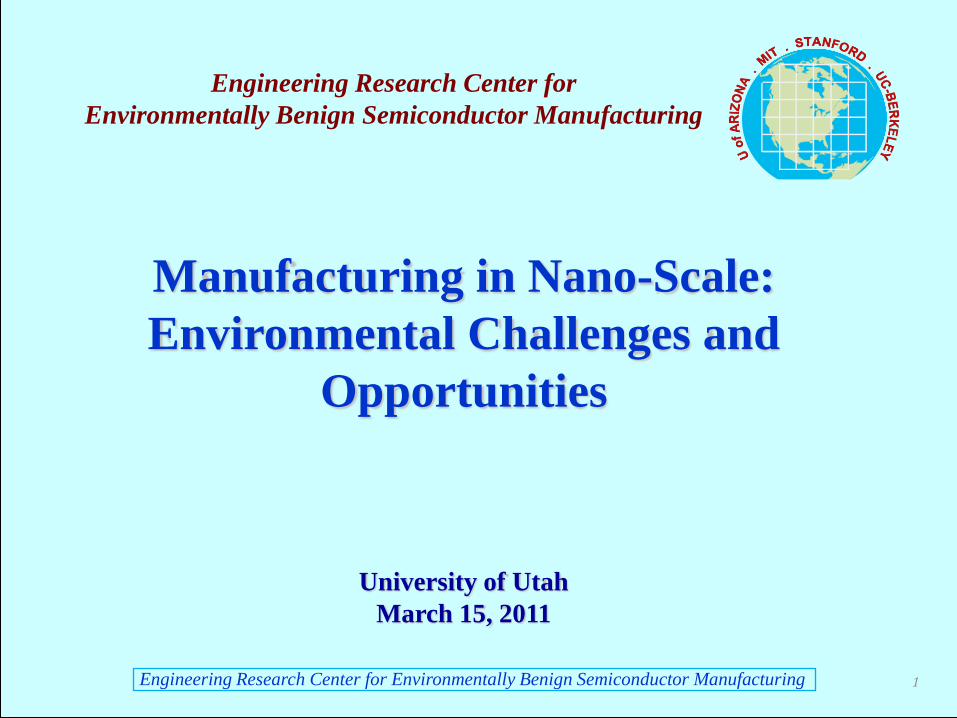
Manufacturing in Nano-Scale:
Environmental Challenges and
Opportunities
University of Utah
March 15, 2011
1
Engineering Research Center for Environmentally Benign Semiconductor Manufacturing
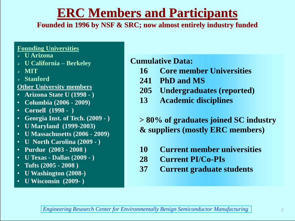
U Arizona
U California – Berkeley
MIT
Stanford
Other University members
• Arizona State U (1998 - )
• Columbia (2006 - 2009)
• Cornell (1998 - )
• Georgia Inst. of Tech. (2009 - )
• U Maryland (1999-2003)
• U Massachusetts (2006 - 2009)
• U North Carolina (2009 - )
• Purdue (2003 - 2008 )
• U Texas - Dallas (2009 - )
• Tufts (2005 - 2008 )
• U Washington (2008-)
• U Wisconsin (2009- )
Founding Universities
Cumulative Data:
16 Core member Universities
241 PhD and MS
205 Undergraduates (reported)
13 Academic disciplines
> 80% of graduates joined SC industry
& suppliers (mostly ERC members)
10 Current member universities
28 Current PI/Co-PIs
37 Current graduate students
ERC Members and Participants Founded in 1996 by NSF & SRC; now almost entirely industry funded
2

Engineering Research Center for Environmentally Benign Semiconductor Manufacturing
A Formidable Economic Ecosystem
Electronics ~ $1.2 T
Semiconductors ~ $250B
~ $5.5T IT-Enabled Services
Suppliers ~ $60B
3

Engineering Research Center for Environmentally Benign Semiconductor Manufacturing
1990 2000 2010 2020 1980 1970
Communication and
Information Management
Computing
Health/Medical
Environmental
Security/Safety
Applications that Have Changed Our World
4
Engineering Research Center for Environmentally Benign Semiconductor Manufacturing
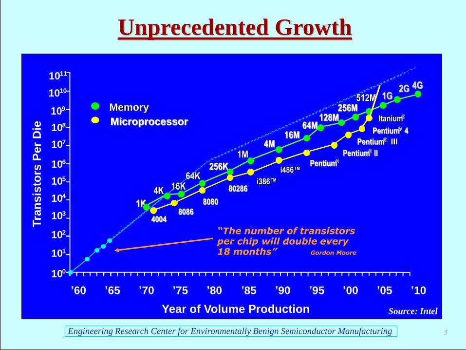
Unprecedented Growth
10 8
10 7
10 6
10 5
10 4
10 3
10 2
10 1
10 0
10 9
10 10
’ 60 ’ 65 ’ 70 ’ 75 ’ 80 ’ 85 ’ 90 ’ 95 ’ 00 ’ 05 ’ 10
Tra
nsis
tors
Per
Die
10 11
1K 1K
4K 4K 16K 16K 64K 64K
256K 256K
1M 1M
16M 16M 4M 4M
64M 64M
4004 4004
8080 8080
8086 8086
80286 80286 i386™ i386™
i486™ i486™ Pentium Pentium ® ®
Memory Memory
Microprocessor Microprocessor
Pentium Pentium ® ® II II
Pentium Pentium ® ® III III
256M 256M 512M 512M
Pentium Pentium ® ® 4
Itanium Itanium ® ®
1G 2G 4G
128M 128M
“The number of transistors per chip will double every 18 months” Gordon Moore
Year of Volume Production Source: Intel
5

Engineering Research Center for Environmentally Benign Semiconductor Manufacturing
Shrinking of Device Dimensions
30 nm
20 nm
25 nm
15nm
15 nm
50 nm length
First MOSFET
(1960)
10-7
MOSFET in 2008
Gate thickness <1 nm
Channel Length <10 nm
Junction depth < 50 nm
Size of an atom ~ 0.5 nm
10 nm
20 mm
6
Engineering Research Center for Environmentally Benign Semiconductor Manufacturing
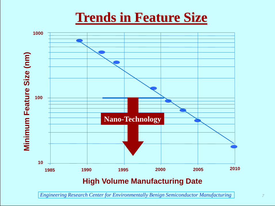
Trends in Feature Size
High Volume Manufacturing Date
Min
imu
m F
eatu
re S
ize (
nm
)
10
100
1000
1985 1990 1995 2000 2005 2010
Nano-Technology
7

Engineering Research Center for Environmentally Benign Semiconductor Manufacturing
Introduction of New Materials
11 Elements
Source: Terrence McManus, Intel
15 Elements
>60 Elements
8
Engineering Research Center for Environmentally Benign Semiconductor Manufacturing
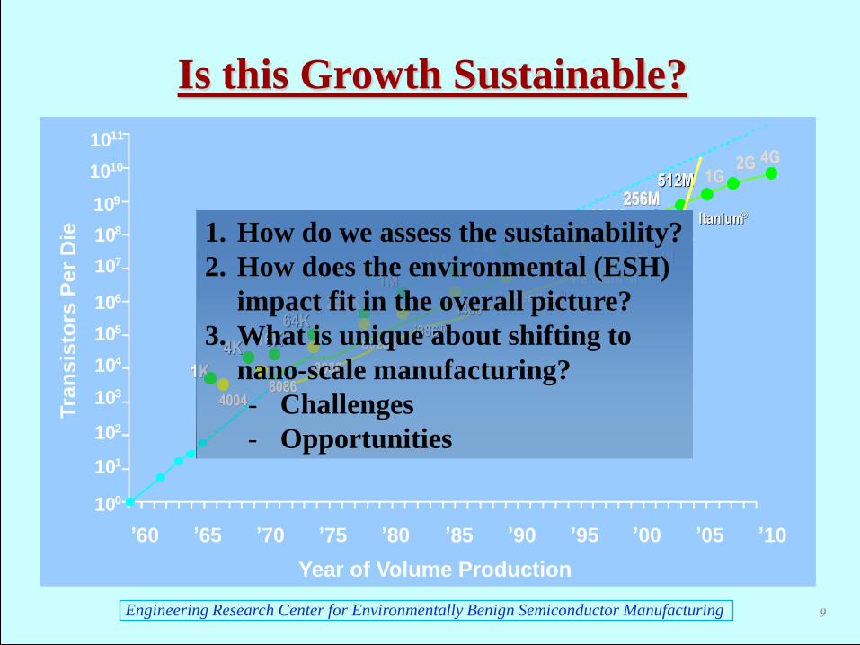
Is this Growth Sustainable?
10 8
10 7
10 6
10 5
10 4
10 3
10 2
10 1
10 0
10 9
10 10
’ 60 ’ 65 ’ 70 ’ 75 ’ 80 ’ 85 ’ 90 ’ 95 ’ 00 ’ 05 ’ 10
Tra
nsis
tors
Per
Die
10 11
64M 64M
256M 256M 512M 512M
Itanium Itanium ® ®
1G 2G 4G
128M 128M
Year of Volume Production
1K 1K
4K 4K 16K 16K 64K 64K
256K 256K
1M 1M
16M 16M 4M 4M
4004 4004
8080 8080
8086 8086
80286 80286 i386™ i386™
i486™ i486™ Pentium Pentium ® ®
Pentium Pentium ® ® II II
Pentium Pentium ® ® III III
Pentium Pentium ® ® 4 1. How do we assess the sustainability?
2. How does the environmental (ESH)
impact fit in the overall picture?
3. What is unique about shifting to
nano-scale manufacturing?
- Challenges
- Opportunities
9
Engineering Research Center for Environmentally Benign Semiconductor Manufacturing
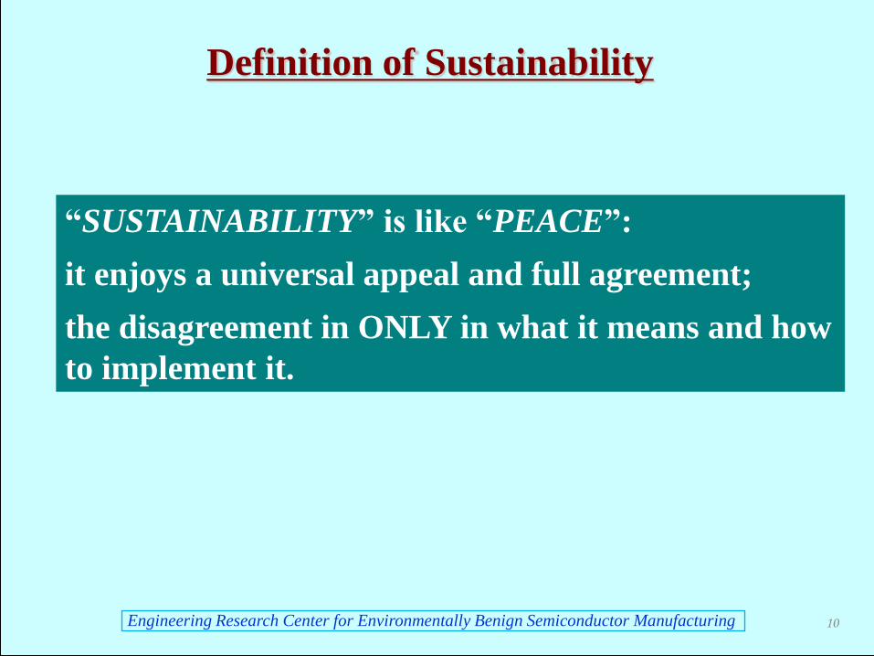
“SUSTAINABILITY” is like “PEACE”:
it enjoys a universal appeal and full agreement;
the disagreement in ONLY in what it means and how
to implement it.
Definition of Sustainability
10

Engineering Research Center for Environmentally Benign Semiconductor Manufacturing
Sustainability Factors
1. Product performance
2. Cost and economic factors
3. Environmental impact
Safety and Health
Social factors and
compatibility
Resource utilization and
availability
Factors that determine the sustainability of a product, a process,
a manufacturing operation, or an industry:
Cost ESH Impact
Performance Obstacles
Upper Level
Constraint
Area of Triangle =
Manufacturing Burden
To be Minimized
Cost ESH Impact
Performance Obstacles
Upper Level
Constraint
Area of Triangle =
Manufacturing Burden
To be Minimized
11

Engineering Research Center for Environmentally Benign Semiconductor Manufacturing
Sustainability
Boundary
Industry
Footprint
(Manufacturing
Burden) P
erfo
rman
ce
Barr
iers
Sustainability Illustrated
12
Engineering Research Center for Environmentally Benign Semiconductor Manufacturing
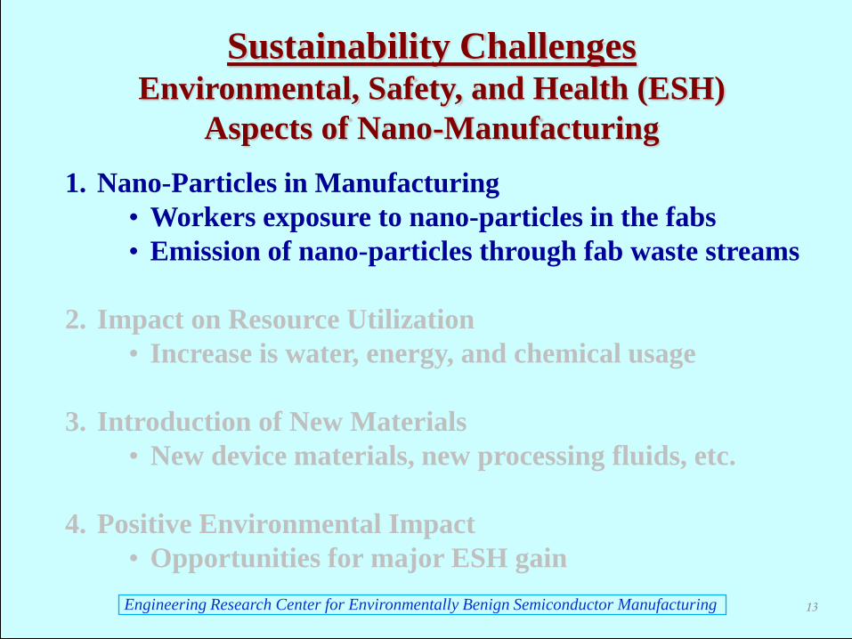
Sustainability Challenges Environmental, Safety, and Health (ESH)
Aspects of Nano-Manufacturing
1. Nano-Particles in Manufacturing
• Workers exposure to nano-particles in the fabs
• Emission of nano-particles through fab waste streams
2. Impact on Resource Utilization
• Increase is water, energy, and chemical usage
3. Introduction of New Materials
• New device materials, new processing fluids, etc.
4. Positive Environmental Impact
• Opportunities for major ESH gain
13

Engineering Research Center for Environmentally Benign Semiconductor Manufacturing
Colorants & Coatings
(Farbe & Lack Journal; April 1949)
New additive for coating industry
Particle size:
4-20 milli-micron (nanometers)
Aerosil = fumed SiO2
Functionalized Fabricated Nano-Particles New name for some old materials
14

Engineering Research Center for Environmentally Benign Semiconductor Manufacturing
What is Unique About Nano-Particles?
• Nano-particles cannot be effectively removed
by agglomeration, settling, and filtration; they
also clog membranes.
• Active surface
• Selective adsorption
• Pore condensation (Kelvin Effect)
Shell
Adsorbed
contaminants
Treatment problem:
Core
o Concentration
o Facilitated transport
o Enhanced life-time Consequence
Synergistic ESH impact of nano-particles:
15
Engineering Research Center for Environmentally Benign Semiconductor Manufacturing
0
0.5
1
1.5
2
2.5
3
1.5 2 2.5 3 3.5
SiO2
HfO2
ZrO2
VO
C a
dso
rpti
on
ca
pa
city
(10
14 m
ole
cule
s/cm
2)
1000/T (K-1)
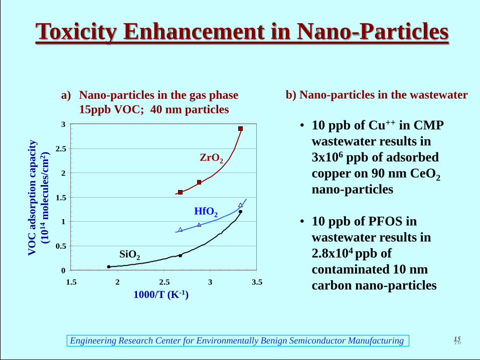
Toxicity Enhancement in Nano-Particles
a) Nano-particles in the gas phase
15ppb VOC; 40 nm particles
• 10 ppb of Cu++ in CMP
wastewater results in
3x10⁶ ppb of adsorbed
copper on 90 nm CeO2
nano-particles
• 10 ppb of PFOS in
wastewater results in
2.8x10⁴ ppb of
contaminated 10 nm
carbon nano-particles
b) Nano-particles in the wastewater
15 16
Engineering Research Center for Environmentally Benign Semiconductor Manufacturing
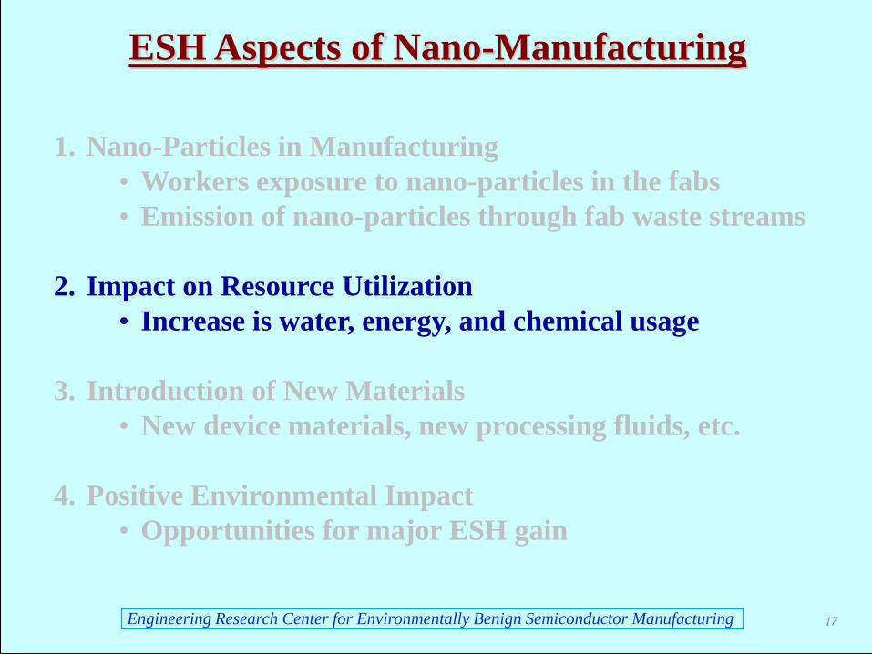
ESH Aspects of Nano-Manufacturing
1. Nano-Particles in Manufacturing
• Workers exposure to nano-particles in the fabs
• Emission of nano-particles through fab waste streams
2. Impact on Resource Utilization
• Increase is water, energy, and chemical usage
3. Introduction of New Materials
• New device materials, new processing fluids, etc.
4. Positive Environmental Impact
• Opportunities for major ESH gain
17
Engineering Research Center for Environmentally Benign Semiconductor Manufacturing
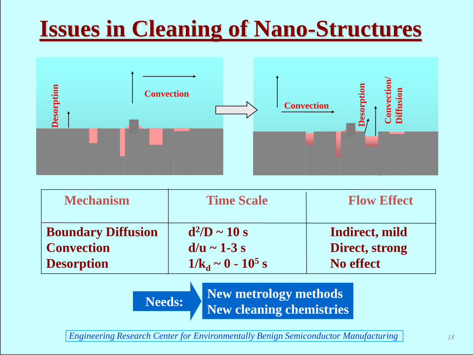
Mechanism Time Scale Flow Effect
Boundary Diffusion d2/D ~ 10 s Indirect, mild
Convection d/u ~ 1-3 s Direct, strong
Desorption 1/kd ~ 0 - 105 s No effect
Des
orp
tio
n
Co
nv
ecti
on
/
Dif
fusi
on
Convection
Des
orp
tio
n
Convection
Issues in Cleaning of Nano-Structures
New metrology methods
New cleaning chemistries Needs:
18

Engineering Research Center for Environmentally Benign Semiconductor Manufacturing
Trench Depth (m)
0.001
0.01
0.1
1
10
0 1 2 3 4 5
Cle
an
ing T
ime
(min
)
1
10
100
1 10 100 1000 10000 100000
Node 1
Req
uir
ed D
ryin
g E
ner
gy
(k
J /
g)
Feature Width, w (nm)
Node 2
Node 3H (enthalpy) of
H2O evaporation0.01
0.1
1
10
100
1 10 100 1000 10000
Trench Width (nm)
Cle
an
ing T
ime
(min
)
ERC results show large increase in
water, chemicals, and energy usage
in various nano-manufacturing
processes as feature size decreases
and wafer size increases.
Large Wafers and Small Features
ESH Challenges
19

Engineering Research Center for Environmentally Benign Semiconductor Manufacturing
A Novel Metrology Technology: Electro-Chemical Residue Sensor (ECRS)
0
0.2
0.4
0.6
0.8
1
0 5 10 15 20 25 30
HCl
H2SO4
0
0.2
0.4
0.6
0.8
1.0
Solution (pH)
(ppt)
UPW (pH=7) HCl (pH=6) HCl (pH=5)
18
5
2.3
30
0.23
400 Resolution
Time (min)
Sen
sor
Ou
tpu
t (%
fu
ll s
ca
le)
0
0.2
0.4
0.6
1.0
Resistivity (MΩ)
Unique Characteristics: • In-situ
• Real time
• On-line
• High sensitivity for small feature sizes
• Very short response time
• Total integration
20

Engineering Research Center for Environmentally Benign Semiconductor Manufacturing
ECRS: Winner of 2009 Product of the year Award
21
Engineering Research Center for Environmentally Benign Semiconductor Manufacturing
Cleaning of Nanostructures Process Simulation
FluxA)CQ(Ct
CV
binb
Poisson equation:
Multi-component species transport equations :
φ)CμzC(Dt
Cii
Fiii
i
where charge density:
Ohm’s law:
ε
ρφ
2
22202222
SdSaS
Ck)C(SCkt
C
i
iiCzF
Surface adsorption and desorption:
ii
Ciλσ
where electrical conductivity:
Convection/
Diffusion
Desorption
Convection
Change in tank concentration :
0 EEσJ
• Surface Charge
• Diffusion
• Surface reaction
• Ionic transport
22

Engineering Research Center for Environmentally Benign Semiconductor Manufacturing
Convection
Dif
fusi
on
wafer
water
Extent of
Cleaning
Time
Dif
fusi
on
wafer
water
Des
orpt
ion
Dominant Operation Parameters:
• Temperature
• Time
• Water Purity
• Additives Dominant
Operation
Parameters:
• Flow
• Mixing Purge Transition Final Surface Cleaning
A Novel Staged Rinse Process
Engineering Research Center for Environmentally Benign Semiconductor Manufacturing
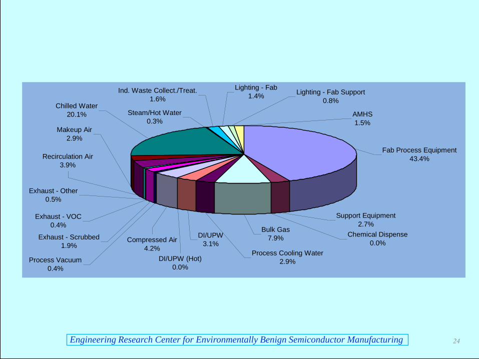
Fab Process Equipment
43.4%
Process Vacuum
0.4%
Compressed Air
4.2%
Exhaust - Scrubbed
1.9%
Makeup Air
2.9%
Steam/Hot Water
0.3%
Ind. Waste Collect./Treat.
1.6%
Lighting - Fab
1.4%Lighting - Fab Support
0.8%
AMHS
1.5%
Chilled Water
20.1%
DI/UPW (Hot)
0.0%
DI/UPW
3.1%
Process Cooling Water
2.9%
Bulk Gas
7.9%
Exhaust - VOC
0.4%
Exhaust - Other
0.5%
Recirculation Air
3.9%
Chemical Dispense
0.0%
Support Equipment
2.7%
24

Engineering Research Center for Environmentally Benign Semiconductor Manufacturing
ESH Aspects of Nano-Manufacturing
1. Nano-Particles in Manufacturing
• Workers exposure to nano-particles in the fabs
• Emission of nano-particles through fab waste streams
2. Impact on Resource Utilization
• Increase is water, energy, and chemical usage
3. Introduction of New Materials
• New device materials, new processing fluids, etc.
4. Positive Environmental Impact
• Opportunities for major ESH gain
25

Engineering Research Center for Environmentally Benign Semiconductor Manufacturing
ESH Impact
and Risk
Introduction of New Materials
Time
Nu
mb
er
26

Engineering Research Center for Environmentally Benign Semiconductor Manufacturing
Introduction of New Materials
Time
Com
ple
xit
y
Si,
SiO2
Al,
SC1
SC2
Compound S/C
Complex dielectrics
Bio-nano electronics
New waste issues
Organo-metallic precursors
ESH Impact
and Risk
Complex PRs and PFOS replacement
27

Engineering Research Center for Environmentally Benign Semiconductor Manufacturing
Environ. Sci. Technol. 2001, 35, 1339.
Environ. Health Perspect. 2005, 113, 539.
Global Distribution of PFOS in Wildlife
• PFOS banned for most application is the US and EU.
• PFOS listed as chemical for regulation within the Stockholm
Convention on Persistent Organic Pollutants (POPs)
• EPA Provisional Health Advisory Levels for PFOS 200 ng L-1
Example: Challenge of Replacing PFOS
PFOS in human blood PFOS in drinking water
PFOS and other PFCs detected in
drinking water resources worldwide
28

Engineering Research Center for Environmentally Benign Semiconductor Manufacturing
aliphatic or aryl unit perfluorinated unit
acid size,
miscibility,
thermal stability,
absorption, outgassing.
acid strength,
absorption photosensitivity,
absorption,
thermal stability.
acid
head
chromophore
Sugar based “Sweet” PAG
Natural molecules based
Biocompatible/ Biodegradable PAG
Hydrophilic
Hydrophobic
Aromatic
Aliphatic
Polar
Nonpolar
Linear branch
ring
Molecular Design of PFOS-Free PAGS
29

Engineering Research Center for Environmentally Benign Semiconductor Manufacturing
ESH Aspects of Nano-Manufacturing
1. Nano-Particles in Manufacturing
• Workers exposure to nano-particles in the fabs
• Emission of nano-particles through fab waste streams
2. Impact on Resource Utilization
• Increase is water, energy, and chemical usage
3. Introduction of New Materials
• New device materials, new processing fluids, etc.
4. Positive Environmental Impact
• Opportunities for major ESH gain
30

Engineering Research Center for Environmentally Benign Semiconductor Manufacturing
Mining
Oil & Gas
Chem/Petrochem
Pharmaceutical
Electronics
Semiconductor
Petroleum Refining
0% 100%
Product Feed Material
Nano-Technology ?
Material Usage Index in Various Industries
31

Engineering Research Center for Environmentally Benign Semiconductor Manufacturing
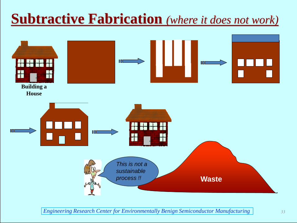
Two Basic Approaches to
Manufacturing Structures
1. Subtractive: Carve the structural details in
a solid block or solid deposited layers
2. Additive: Place the final materials only in
places where they are needed.
32
Engineering Research Center for Environmentally Benign Semiconductor Manufacturing
Subtractive Fabrication (where it does not work)
Building a
House
This is not a
sustainable
process !! Waste
33

Engineering Research Center for Environmentally Benign Semiconductor Manufacturing
ESH
Issues
Precursors, HAPs, wastes
VOCs, radiation
VOCs, waste
VOCs, HAPs
HAPs, PFCs
A/B chemicals, solvents
A/B chemicals, UPW
Conventional Lithography
development in aqueous base
spin-on imaging layer
dielectric deposition
selective irradiation
dielectric patterning
imaging layer strip
resist strip
An Example of Subtractive Processing Deposition and Patterning of Dielectrics
34

Engineering Research Center for Environmentally Benign Semiconductor Manufacturing
TiCl4 H2O TiO2
+
Conventional Subtractive Processing
Deposition
35

Engineering Research Center for Environmentally Benign Semiconductor Manufacturing
Conventional Subtractive Processing
Planarization
TiCl4 H2O TiO2
+
Waste
36

Engineering Research Center for Environmentally Benign Semiconductor Manufacturing
TiCl4 H2O TiO2
+
Waste
Conventional Subtractive Processing
Photo-Resist
37
Engineering Research Center for Environmentally Benign Semiconductor Manufacturing
TiCl4 H2O TiO2
+
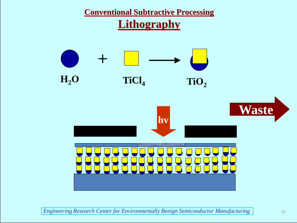
hv
Conventional Subtractive Processing
Lithography
Waste
38

Engineering Research Center for Environmentally Benign Semiconductor Manufacturing
TiCl4 H2O TiO2
+
Etch
Conventional Subtractive Processing
Etch
Waste
39
Engineering Research Center for Environmentally Benign Semiconductor Manufacturing
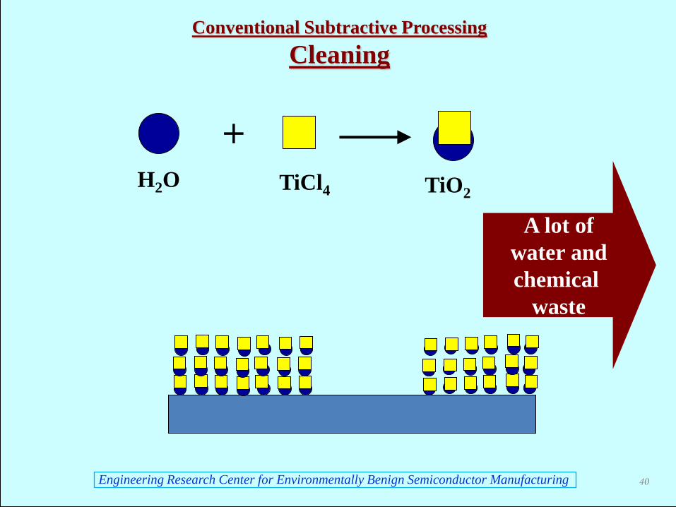
TiCl4 H2O TiO2
+
A lot of
water and
chemical
waste
Conventional Subtractive Processing
Cleaning
40

Engineering Research Center for Environmentally Benign Semiconductor Manufacturing
Additive Processing:
Patterning and Selective Passivation
hv
Selective passivation
41
Engineering Research Center for Environmentally Benign Semiconductor Manufacturing
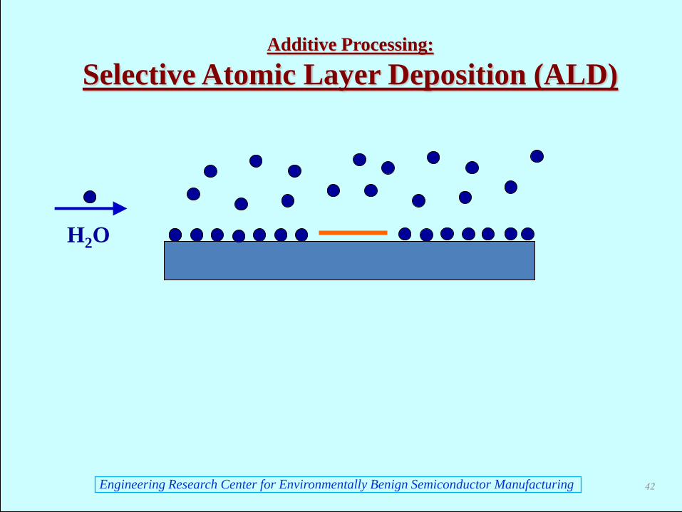
H2O
Additive Processing:
Selective Atomic Layer Deposition (ALD)
42

Engineering Research Center for Environmentally Benign Semiconductor Manufacturing
Additive Processing:
Selective Atomic Layer Deposition (ALD)
43
Engineering Research Center for Environmentally Benign Semiconductor Manufacturing
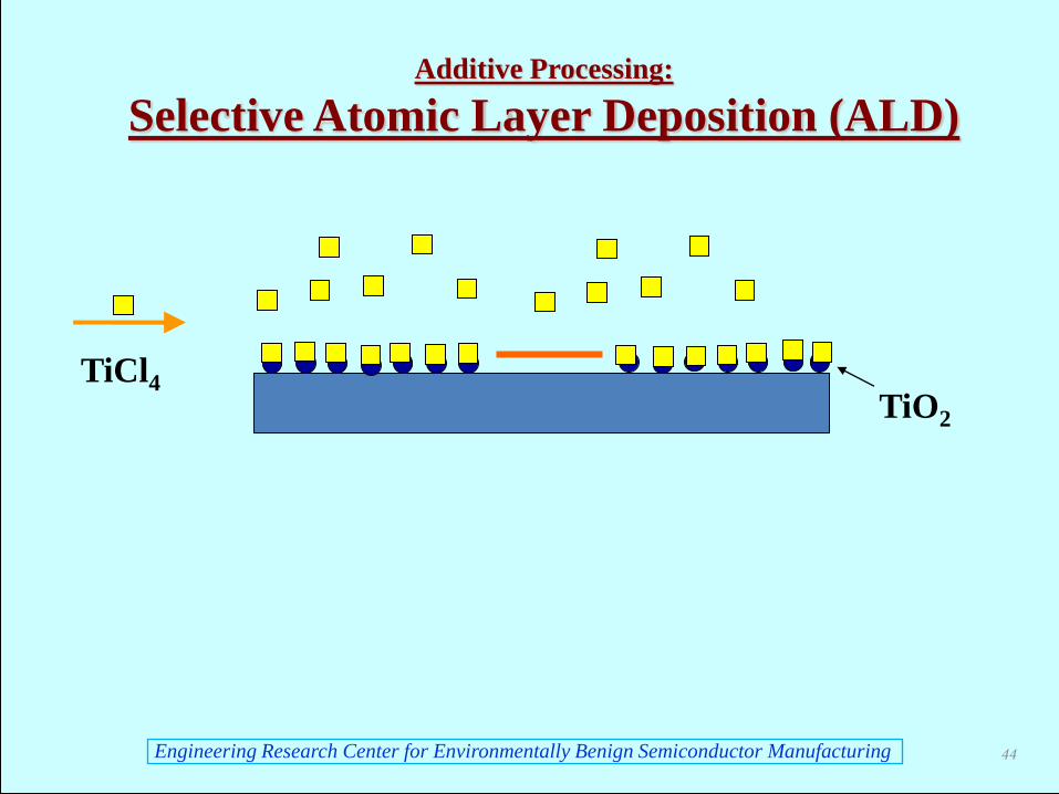
TiCl4
TiO2
Additive Processing:
Selective Atomic Layer Deposition (ALD)
44
Engineering Research Center for Environmentally Benign Semiconductor Manufacturing
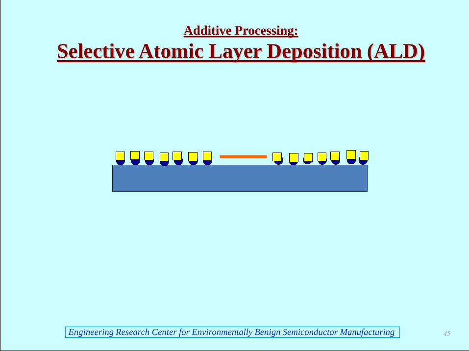
Additive Processing:
Selective Atomic Layer Deposition (ALD)
45

Engineering Research Center for Environmentally Benign Semiconductor Manufacturing
Additive Processing:
Selective Atomic Layer Deposition (ALD)
46
Engineering Research Center for Environmentally Benign Semiconductor Manufacturing
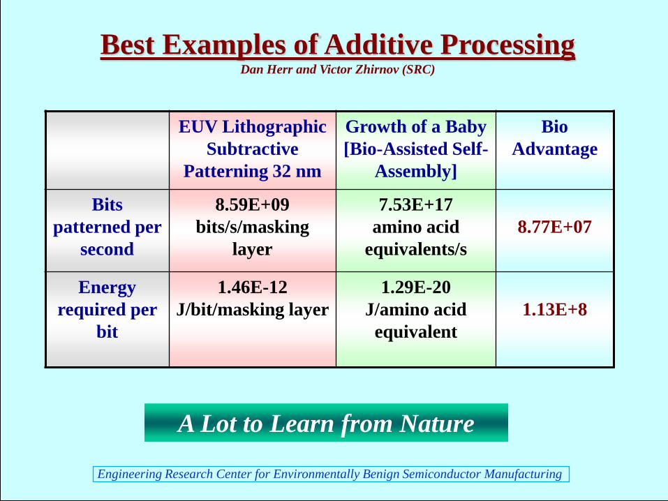
Best Examples of Additive Processing Dan Herr and Victor Zhirnov (SRC)
A Lot to Learn from Nature
EUV Lithographic
Subtractive
Patterning 32 nm
Growth of a Baby
[Bio-Assisted Self-
Assembly]
Bio
Advantage
Bits
patterned per
second
8.59E+09
bits/s/masking
layer
7.53E+17
amino acid
equivalents/s
8.77E+07
Energy
required per
bit
1.46E-12
J/bit/masking layer
1.29E-20
J/amino acid
equivalent
1.13E+8

Engineering Research Center for Environmentally Benign Semiconductor Manufacturing NSF/SRC Engineering Research Center for Environmentally Benign Semiconductor Manufacturing
ERC Website
www.erc.arizona.edu
Email:
Thank you
48