Embed Size (px)
Citation preview
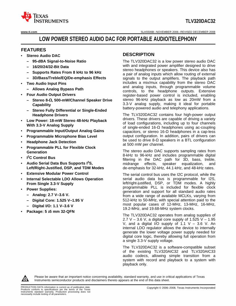
1FEATURESDESCRIPTION
TLV320DAC32
www.ti.com........................................................................................................................................ SLAS506B–NOVEMBER 2006–REVISED DECEMBER 2008
LOW POWER STEREO AUDIO DAC FOR PORTABLE AUDIO/TELEPHONY
• Stereo Audio DAC– 95-dBA Signal-to-Noise Ratio The TLV320DAC32 is a low power stereo audio DAC
with and integrated power amplifier designed to drive– 16/20/24/32-Bit Datastereo headphones or speakers. This device also has– Supports Rates From 8 kHz to 96 kHz a pair of analog inputs which allow routing of external
– 3D/Bass/Treble/EQ/De-emphasis Effects signals to the output amplifiers. The playback pathincludes a mix/mux capability from the stereo DAC• Two Audio Input Pinsand analog inputs, through programmable volume– Allows Analog Bypass Path controls, to the headphone outputs. Extensive
• Four Audio Output Drivers register-based power control is included, enablingstereo 96-kHz playback as low as 20mW from a– Stereo 8-Ω, 500-mW/Channel Speaker Drive3.3-V analog supply, making it ideal for portableCapabilitybattery-powered audio and telephony applications.– Stereo Fully Differential or Single-EndedThe TLV320DAC32 contains four high-power outputHeadphone Driversdrivers. These drivers are capable of driving a variety• Low Power: 18-mW Stereo 48-kHz Playback of load configurations, including up to four channelsWith 3.3-V Analog Supply of single-ended 16-Ω headphones using ac-coupling
• Programmable Input/Output Analog Gains capacitors, or stereo 16-Ω headphones in a cap-lessoutput configuration. In addition, pairs of drivers can• Programmable Microphone Bias Levelbe used to drive 8-Ω speakers in a BTL configuration• Headphone Jack Detection at 500 mW per channel.
• Programmable PLL for Flexible ClockThe stereo audio DAC supports sampling rates fromGeneration8-kHz to 96-kHz and includes programmable digital• I2C Control Bus filtering in the DAC path for 3D, bass, treble,
• Audio Serial Data Bus Supports I2S, midrange effects, speaker equalization, andLeft/Right-Justified, DSP, and TDM Modes de-emphasis for 32-kHz, 44.1-kHz, and 48-kHz rates.
• Extensive Modular Power Control The serial control bus uses the I2C protocol, while theserial audio data bus is programmable for I2S,• Internal Selectable LDO Allows Operationleft/right-justified, DSP, or TDM modes. A highlyFrom Single 3.3-V Supplyprogrammable PLL is included for flexible clock• Power Supplies: generation and support for all standard audio rates
– Analog: 2.7 V–3.6 V. from a wide range of available MCLKs, varying from512-kHz to 50-MHz, with special attention paid to the– Digital Core: 1.525 V–1.95 Vmost popular cases of 12-MHz, 13-MHz, 16-MHz,– Digital I/O: 1.1 V–3.6 V19.2-MHz, and 19.68-MHz system clocks.
• Package: 5 5נ mm 32-QFNThe TLV320DAC32 operates from analog supplies of2.7 V – 3.6 V, a digital core supply of 1.525 V – 1.95V, and a digital I/O supply of 1.1 V – 3.6 V. Aninternal LDO regulator allows the device to internallygenerate the lower voltage power supply needed fordigital core logic, thereby allowing full operation froma single 3.3-V supply voltage.
The TLV320DAC32 is a software-compatible subsetof the existing TLV320AIC32 and TLV320AIC33audio codecs, allowing simple transition from asystem with record and playback to a system withplayback only.
1
Please be aware that an important notice concerning availability, standard warranty, and use in critical applications of TexasInstruments semiconductor products and disclaimers thereto appears at the end of this data sheet.
PRODUCTION DATA information is current as of publication date. Copyright © 2006–2008, Texas Instruments IncorporatedProducts conform to specifications per the terms of the TexasInstruments standard warranty. Production processing does notnecessarily include testing of all parameters.
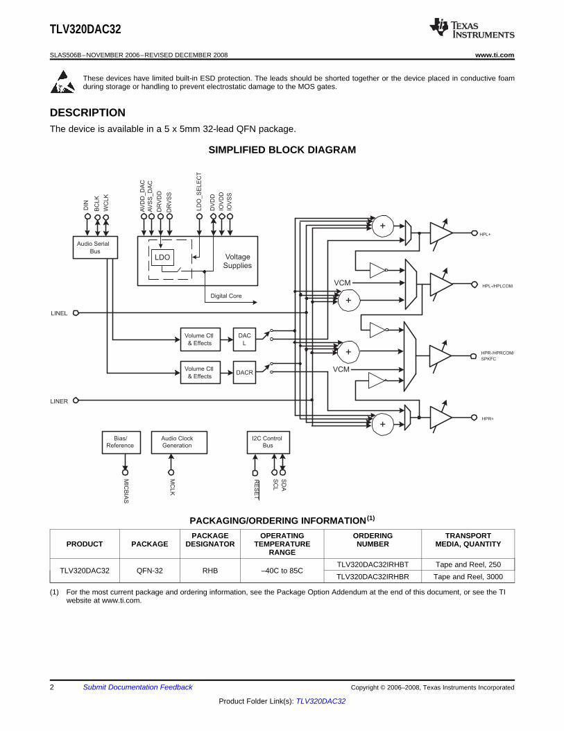
DESCRIPTION
SIMPLIFIED BLOCK DIAGRAM
HPR+
HPL-/HPLCOM
HPL+
LINEL
DAC
L
DACR
I2C Control
Bus
Audio Clock
Generation
MC
LK
Bias/
ReferenceM
ICB
IAS
Volume Ctl
& Effects
Volume Ctl
& Effects
SC
L
SD
A
RE
SE
T
LINER
+
+
VCM
+
HPR-/HPRCOM/
SPKFC+
VCM
Audio Serial
Bus
DIN
BC
LK
WC
LK
AV
DD
_D
AC
AV
SS
_D
AC
DR
VD
D
DR
VS
S
VoltageSupplies
LDO
Digital Core
LD
O_
SE
LE
CT
DV
DD
IOV
DD
IOV
SS
TLV320DAC32
SLAS506B–NOVEMBER 2006–REVISED DECEMBER 2008........................................................................................................................................ www.ti.com
These devices have limited built-in ESD protection. The leads should be shorted together or the device placed in conductive foamduring storage or handling to prevent electrostatic damage to the MOS gates.
The device is available in a 5 x 5mm 32-lead QFN package.
PACKAGING/ORDERING INFORMATION (1)
PACKAGE OPERATING ORDERING TRANSPORTPRODUCT PACKAGE DESIGNATOR TEMPERATURE NUMBER MEDIA, QUANTITY
RANGETLV320DAC32IRHBT Tape and Reel, 250
TLV320DAC32 QFN-32 RHB –40C to 85CTLV320DAC32IRHBR Tape and Reel, 3000
(1) For the most current package and ordering information, see the Package Option Addendum at the end of this document, or see the TIwebsite at www.ti.com.
2 Submit Documentation Feedback Copyright © 2006–2008, Texas Instruments Incorporated
Product Folder Link(s): TLV320DAC32
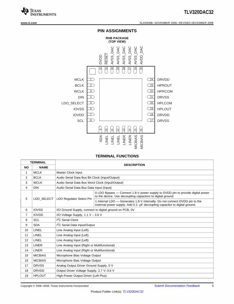
PIN ASSIGNMENTS
24
23
22
21
20
19
18
17
1
2
3
4
5
6
7
8
9 10 11 12 13 14 15 16
MCLK
BCLK
WCLK
DIN
LDO_SELECT
IOVSS
IOVDD
SCL
DRVDD
HPROUT
HPRCOM
DRVSS
HPLCOM
HPLOUT
DRVDD
DRVSS
32 31 30 29 28 27 26 25
DV
DD
RE
SE
T
AV
SS
_DA
C
AV
SS
_DA
C
AV
SS
_DA
C
AV
SS
_DA
C
AV
SS
_DA
C
AV
DD
_DA
C
SD
A
LIN
EL
LIN
EL
LIN
EL
LIN
ER
LIN
ER
MIC
BIA
S
MIC
BIA
S
TLV320DAC32
www.ti.com........................................................................................................................................ SLAS506B–NOVEMBER 2006–REVISED DECEMBER 2008
RHB PACKAGE(TOP VIEW)
TERMINAL FUNCTIONSTERMINAL
DESCRIPTIONNO NAME1 MCLK Master Clock Input2 BCLK Audio Serial Data Bus Bit Clock (Input/Output)3 WCLK Audio Serial Data Bus Word Clock (Input/Output)4 DIN Audio Serial Data Bus Data Input (Input)
0 LDO Bypass — Connect 1.8-V power supply to DVDD pin to provide digital powerto the device. Use decoupling capacitors to digital ground.
5 LDO_SELECT LDO Regulator Select Pin1 Internal LDO — Generates 1.8-V internally. Do not connect DVDD pin to theexternal power supply. Add 0.1- µF decoupling capacitor to digital ground.
6 IOVSS I/O Ground Supply, connect to digital ground on PCB, 0V7 IOVDD I/O Voltage Supply, 1.1 V – 3.6 V8 SCL I2C Serial Clock9 SDA I2C Serial Data Input/Output10 LINEL Line Analog Input (Left)11 LINEL Line Analog Input (Left)12 LINEL Line Analog Input (Left)13 LINER Line Analog Input (Right or Multifunctional)14 LINER Line Analog Input (Right or Multifunctional)15 MICBIAS Microphone Bias Voltage Output16 MICBIAS Microphone Bias Voltage Output17 DRVSS Analog Output Driver Ground Supply, 0 V18 DRVDD Output Driver Voltage Supply, 2.7 V–3.6 V19 HPLOUT High-Power Output Driver (Left Plus)
Copyright © 2006–2008, Texas Instruments Incorporated Submit Documentation Feedback 3
Product Folder Link(s): TLV320DAC32
ABSOLUTE MAXIMUM RATINGS
DISSIPATION RATINGS (1)
TLV320DAC32
SLAS506B–NOVEMBER 2006–REVISED DECEMBER 2008........................................................................................................................................ www.ti.com
TERMINAL FUNCTIONS (continued)TERMINAL
DESCRIPTIONNO NAME20 HPLCOM High-Power Output Driver (Left Minus or Multifunctional)21 DRVSS Analog Output Driver Ground Supply, 0 V22 HPRCOM High-Power Output Driver (Right Minus or Multifunctional)23 HPROUT High-Power Output Driver (Right Plus)24 DRVDD Output Driver Voltage Supply, 2.7 V–3.6 V25 AVDD_DAC Analog and DAC Voltage Supply, 2.7 V–3.6 V
26,27,28,29, AVSS_DAC Analog and DAC Ground Supply, 0 V
3031 RESET Reset
Digital Core Voltage Supply, add 0.1-µF capacitor to digital ground. Connect to 1.8-V power supply if32 DVDD LDO_SELECT = 0 V.
over operating free-air temperature range (unless otherwise noted) (1) (2)
VALUE UNITAVDD_DAC to AVSS_DAC, DRVDD to DRVSS –0.3 to 3.9 VAVDD_DAC to DRVSS –0.3 to 3.9 VIOVDD to IOVSS –0.3 to 3.9 VDVDD to IOVSS –0.3 to 2.5 VAVDD_DAC to DRVDD –0.1 to 0.1 VDigital input voltage to IOVSS –0.3 V to IOVDD+0.3 VAnalog input voltage to AVSS_DAC –0.3 V to AVDD_DAC+0.3 VOperating temperature range -40 to +85 CStorage temperature range -65 to +105 C
TJ Max Junction temperature 105 CPower dissipation (TJ Max – TA) / θJA
θJA Thermal impedance 44 C/W
(1) Stresses beyond those listed under absolute maximum ratings may cause permanent damage to the device. These are stress ratingsonly, and functional operation of the device at these or any other conditions beyond those indicated under recommended operatingconditions is not implied. Exposure to absolute-maximum-rated conditions for extended periods may affect device reliability.
(2) ESD compliance tested to EIA / JESD22-A114-B and passed.
TA = 25C TA = 75C TA = 85CDERATING FACTORPOWER RATING POWER RATING POWER RATING1.82 W 22.7 mW/C 681 mW 454 mW
(1) This data was taken using 2 oz. trace and copper pad that is soldered directly to a JEDEC standard 4-layer 3 in 3נ in PCB.
4 Submit Documentation Feedback Copyright © 2006–2008, Texas Instruments Incorporated
Product Folder Link(s): TLV320DAC32
RECOMMENDED OPERATING CONDITIONS
ELECTRICAL CHARACTERISTICS
TLV320DAC32
www.ti.com........................................................................................................................................ SLAS506B–NOVEMBER 2006–REVISED DECEMBER 2008
over operating free-air temperature range (unless otherwise noted)
MIN NOM MAX UNITAVDD_DAC, Analog supply voltage 2.7 3.3 3.6 VDRVDD (1)
DVDD (1) Digital core supply voltage 1.525 1.8 1.95 VIOVDD (1) Digital I/O supply voltage 1.1 1.8 3.6 VVI Analog full-scale 0-dB input voltage (DRVDD = 3.3 V) 0.707 VRMS
Stereo headphone-output load resistance 16 ΩDigital output load capacitance 10 pF
TA Operating free-air temperature –40 85 C
(1) Analog voltage values are with respect to AVSS_DAC, DRVSS; digital voltage values are with respect to IOVSS.
At 25C, AVDD_DAC, DRVDD, IOVDD = 3.3 V, DVDD = 1.8 V, Fs = 48 kHz, 16-bit audio data (unless otherwise noted)
PARAMETER TEST CONDITIONS MIN TYP MAX UNITANALOG MIXER
Input resistance LINE inputs 100 kΩInput capacitance LINE inputs 10 pFInput volume controlminimum attenuation 0 dBsettingInput volume controlmaximum attenuation 78 dBsettingInput volume control 0.5 dBattenuation step size
MICROPHONE BIAS2.0
2.25 2.5 2.75Bias voltage Programmable settings, load = 750 Ω VDRVDD-
0.2Current sourcing 2.5-V Setting 4 mA
DAC DIGITALINTERPOLATION Fs = 48 kHzFILTER
Passband High-pass filter disabled 0.45Ӧs HzPassband ripple High-pass filter disabled 0.06 dBTransition band 0.45Ӧs 0.55Ӧs HzStopband 0.55Ӧs 7.5Ӧs HzStopband attenuation 65 dBGroup delay 21/Fs Sec
SINGLE-ENDED STEREO AC-coupled output configuration (1)HEADPHONE DRIVER
0-dB full-scale output 0-dB Gain to high power outputs. Output 0.65 VRMSvoltage common-mode voltage setting = 1.65 VFirst option 1.35
Programmable outputSecond option 1.50common mode voltage V(applicable to Line Third option 1.65
Outputs also)Fourth option 1.8
(1) Unless otherwise noted, all measurements use output common-mode voltage setting of 1.35 V, 0-dB output level control gain, 16-Ωsingle-ended load.
Copyright © 2006–2008, Texas Instruments Incorporated Submit Documentation Feedback 5
Product Folder Link(s): TLV320DAC32
TLV320DAC32
SLAS506B–NOVEMBER 2006–REVISED DECEMBER 2008........................................................................................................................................ www.ti.com
ELECTRICAL CHARACTERISTICS (continued)At 25C, AVDD_DAC, DRVDD, IOVDD = 3.3 V, DVDD = 1.8 V, Fs = 48 kHz, 16-bit audio data (unless otherwise noted)
PARAMETER TEST CONDITIONS MIN TYP MAX UNITMaximumprogrammable output 9 dBlevel control gainProgrammable outputlevel control gain step 1 dBsize
RL = 32 Ω, 0.1% THD 25PO Maximum output power mW
RL = 16 Ω, 0.1% THD 50SNR Signal-to-noise ratio (2) 85 94 dB
–79 –60Total harmonic 1-kHz Output, PO = 26 mW, RL = 16 Ω dB%distortion 0.011Channel separation 1 kHz, 0-dB Input 85 dBPower supply rejection 1 KHz, 100 mVpp on AVDD_DAC, DRVDD1/2 52 dBratioMute attenuation 1-kHz Output 107 dB
DIFFERENTIAL STEREO HEADPHONE DRIVER0-dB Gain to high power outputs. Output0-dB full-scale output common-mode voltage setting = 1.65 V, 1.27 Vvoltage Differential output configuration (3)
SNR Signal-to-noise ratio (4) 95 dBDIFFERENTIAL SPEAKER DRIVER
DRVDD = 3.6 V, HPLCOM = 1.8 V,PO Maximum output power 0.5 WHPLCOM/HPRCOM Gain = 5, RL = 8 Ω0-dB Full-scale output 0-dB Gain for HPLCOM/HPRCOM, 1.15 Vrmsvoltage Output common-mode voltage setting = 1.65 V, RL = 8 ΩTotal harmonic Fs = 48 kHz, 0-dB Full-scale signal, –71 dBdistortion 0-dB Gain at HPLCOM/HPRCOM, RL = 8 Ω
DIGITAL I/O0.3VIL Input low level IIL = +5 µA –0.3 VנIOVDD
0.7IIH = +5 µA, IOVDD > 1.6 V IOVDDVIHנ Input high level (5) VIIH = +5 µA, IOVDD < 1.6 V IOVDD
0.1VOL Output low level IIH = 2 TTL loads VנIOVDD0.8VOH Output high level IOH = 2 TTL loads VנIOVDD
SUPPLY CURRENTAVDD_DAC+DRVDD 3.99
Current DVDD 0.025 mALINEL/R only routed to single-endedstereo headphones, DAC = off, AnalogIOVDD 0.001Headphone Mixer = on, PLL = off, LDO = off,amplifier AVDD_DAC+DRVDD 13.17analog mixer enabled, no signalappliedPower DVDD 0.045 mW
IOVDD 0.003
(2) Ratio of output level with a 1-kHz full-scale input, to the output level playing an all-zero signal, measured , A-weighted over a 20-Hz to20-kHz bandwidth.
(3) Unless otherwise noted, all measurements use output common-mode voltage setting of 1.35 V, 0-dB output level control gain, 16-Ωdifferential load.
(4) Ratio of output level with a 1-kHz full-scale input, to the output level playing an all-zero signal, measured , A-weighted over a 20-Hz to20-kHz bandwidth.
(5) When IOVDD < 1.6 V, minimum VIH is 1.1 V.
6 Submit Documentation Feedback Copyright © 2006–2008, Texas Instruments Incorporated
Product Folder Link(s): TLV320DAC32
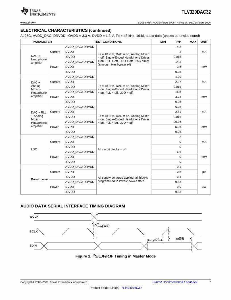
AUDIO DATA SERIAL INTERFACE TIMING DIAGRAM
ts(DI) th(DI)
WCLK
BCLK
SDIN
td(WS)
TLV320DAC32
www.ti.com........................................................................................................................................ SLAS506B–NOVEMBER 2006–REVISED DECEMBER 2008
ELECTRICAL CHARACTERISTICS (continued)At 25C, AVDD_DAC, DRVDD, IOVDD = 3.3 V, DVDD = 1.8 V, Fs = 48 kHz, 16-bit audio data (unless otherwise noted)
PARAMETER TEST CONDITIONS MIN TYP MAX UNITAVDD_DAC+DRVDD 4.3
Current DVDD 2 mAFs = 48 kHz, DAC = on, Analog MixerDAC + IOVDD 0.015= off, Single-Ended Headphone DriverHeadphone = on, PLL = off, LDO = off, DAC directAVDD_DAC+DRVDD 14.2amplifier (analog mixer bypassed)
Power DVDD 3.6 mWIOVDD 0.05AVDD_DAC+DRVDD 4.99
Current DVDD 2.07 mADAC +Analog Fs = 48 kHz, DAC = on, Analog MixerIOVDD 0.015Mixer + = on, Single-Ended Headphone Driver
AVDD_DAC+DRVDD 16.5Headphone = on, PLL = off, LDO = offamplifier Power DVDD 3.73 mW
IOVDD 0.05AVDD_DAC+DRVDD 6.08
Current DVDD 2.81 mADAC + PLL+ Analog Fs = 48 kHz, DAC = on, Analog MixerIOVDD 0.016Mixer + = on, Single-Ended Headphone Driver
AVDD_DAC+DRVDD 20.06Headphone = on, PLL = on, LDO = offamplifier Power DVDD 5.06 mW
IOVDD 0.05AVDD_DAC+DRVDD 2
Current DVDD 0 mAIOVDD 0
LDO All circuit blocks = offAVDD_DAC+DRVDD 6.6
Power DVDD 0 mWIOVDD 0AVDD_DAC+DRVDD 0.1
Current DVDD 0.5 µAIOVDD 0.1All supply voltages applied, all blocksPower down programmed in lowest power stateAVDD_DAC+DRVDD 0.33
Power DVDD 0.9 µWIOVDD 0.33
Figure 1. I2S/LJF/RJF Timing in Master Mode
Copyright © 2006–2008, Texas Instruments Incorporated Submit Documentation Feedback 7
Product Folder Link(s): TLV320DAC32
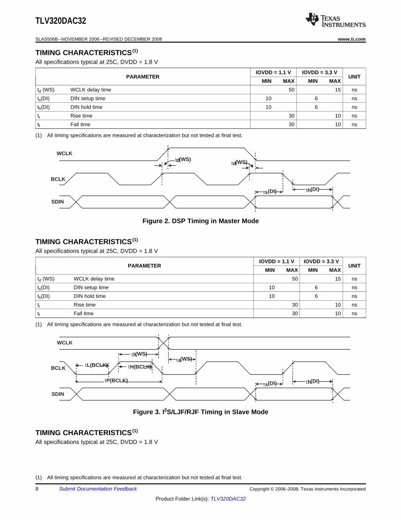
TIMING CHARACTERISTICS (1)
ts(DI) th(DI)
WCLK
BCLK
SDIN
td(WS)td(WS)
TIMING CHARACTERISTICS (1)
th(WS)ts(WS)
ts(DI) th(DI)
WCLK
BCLK
SDIN
tL(BCLK) tH(BCLK)
tP(BCLK)
TIMING CHARACTERISTICS (1)
TLV320DAC32
SLAS506B–NOVEMBER 2006–REVISED DECEMBER 2008........................................................................................................................................ www.ti.com
All specifications typical at 25C, DVDD = 1.8 V
IOVDD = 1.1 V IOVDD = 3.3 VPARAMETER UNIT
MIN MAX MIN MAXtd (WS) WCLK delay time 50 15 nsts(DI) DIN setup time 10 6 nsth(DI) DIN hold time 10 6 nstr Rise time 30 10 nstf Fall time 30 10 ns
(1) All timing specifications are measured at characterization but not tested at final test.
Figure 2. DSP Timing in Master Mode
All specifications typical at 25C, DVDD = 1.8 V
IOVDD = 1.1 V IOVDD = 3.3 VPARAMETER UNIT
MIN MAX MIN MAXtd (WS) WCLK delay time 50 15 nsts(DI) DIN setup time 10 6 nsth(DI) DIN hold time 10 6 nstr Rise time 30 10 nstf Fall time 30 10 ns
(1) All timing specifications are measured at characterization but not tested at final test.
Figure 3. I2S/LJF/RJF Timing in Slave Mode
All specifications typical at 25C, DVDD = 1.8 V
(1) All timing specifications are measured at characterization but not tested at final test.
8 Submit Documentation Feedback Copyright © 2006–2008, Texas Instruments Incorporated
Product Folder Link(s): TLV320DAC32
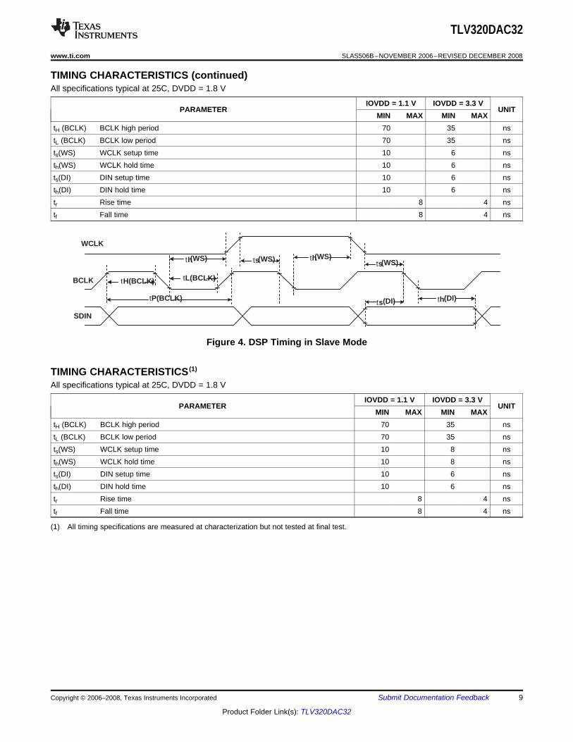
th(WS) ts(WS)
ts(DI) th(DI)
WCLK
BCLK
SDIN
tH(BCLK) tL(BCLK)
tP(BCLK)
ts(WS)th(WS)
TIMING CHARACTERISTICS (1)
TLV320DAC32
www.ti.com........................................................................................................................................ SLAS506B–NOVEMBER 2006–REVISED DECEMBER 2008
TIMING CHARACTERISTICS (continued)All specifications typical at 25C, DVDD = 1.8 V
IOVDD = 1.1 V IOVDD = 3.3 VPARAMETER UNIT
MIN MAX MIN MAXtH (BCLK) BCLK high period 70 35 nstL (BCLK) BCLK low period 70 35 nsts(WS) WCLK setup time 10 6 nsth(WS) WCLK hold time 10 6 nsts(DI) DIN setup time 10 6 nsth(DI) DIN hold time 10 6 nstr Rise time 8 4 nstf Fall time 8 4 ns
Figure 4. DSP Timing in Slave Mode
All specifications typical at 25C, DVDD = 1.8 V
IOVDD = 1.1 V IOVDD = 3.3 VPARAMETER UNIT
MIN MAX MIN MAXtH (BCLK) BCLK high period 70 35 nstL (BCLK) BCLK low period 70 35 nsts(WS) WCLK setup time 10 8 nsth(WS) WCLK hold time 10 8 nsts(DI) DIN setup time 10 6 nsth(DI) DIN hold time 10 6 nstr Rise time 8 4 nstf Fall time 8 4 ns
(1) All timing specifications are measured at characterization but not tested at final test.
Copyright © 2006–2008, Texas Instruments Incorporated Submit Documentation Feedback 9
Product Folder Link(s): TLV320DAC32
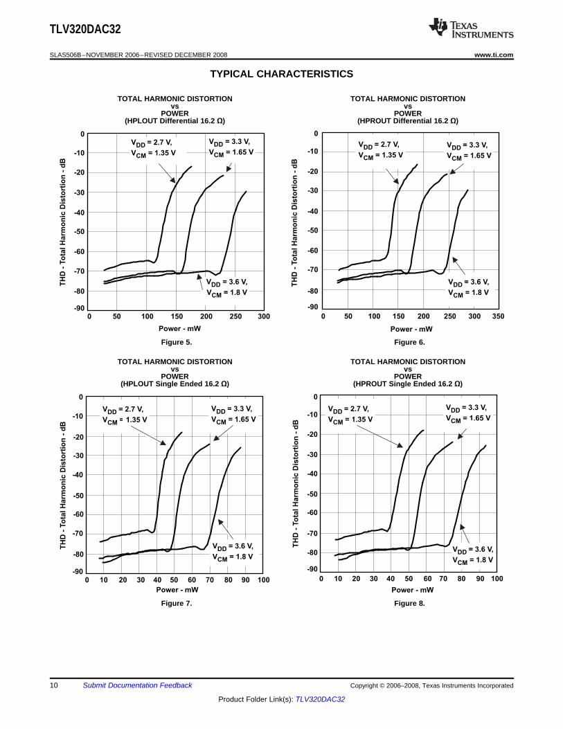
TYPICAL CHARACTERISTICS
V = 2.7 V,
V = 1.35 VDD
CM
V = 3.3 V,
V = 1.65 VDD
CM
V = 3.6 V,
V = 1.8 VDD
CM
-90
-80
-70
-60
-50
-40
-30
-20
-10
0
0 50 100 150 200 250 300
Power - mW
TH
D -
To
tal H
arm
on
ic D
isto
rtio
n -
dB
-90
-80
-70
-60
-50
-40
-30
-20
-10
0
0 50 100 150 200 250 300 350
Power - mW
TH
D -
To
tal H
arm
on
ic D
isto
rtio
n -
dB
V = 2.7 V,
V = 1.35 VDD
CM
V = 3.3 V,
V = 1.65 VDD
CM
V = 3.6 V,
V = 1.8 VDD
CM
-90
-80
-70
-60
-50
-40
-30
-20
-10
0
0 10 20 30 40 50 60 70 80 90 100
Power - mW
TH
D -
To
tal
Ha
rmo
nic
Dis
tort
ion
- d
B
V = 2.7 V,
V = 1.35 VDD
CM
V = 3.3 V,
V = 1.65 VDD
CM
V = 3.6 V,
V = 1.8 VDD
CM
-90
-80
-70
-60
-50
-40
-30
-20
-10
0
0 10 20 30 40 50 60 70 80 90 100
Power - mW
TH
D -
To
tal
Ha
rmo
nic
Dis
tort
ion
- d
B
V = 2.7 V,
V = 1.35 VDD
CM
V = 3.3 V,
V = 1.65 VDD
CM
V = 3.6 V,
V = 1.8 VDD
CM
TLV320DAC32
SLAS506B–NOVEMBER 2006–REVISED DECEMBER 2008........................................................................................................................................ www.ti.com
TOTAL HARMONIC DISTORTION TOTAL HARMONIC DISTORTIONvs vs
POWER POWER(HPLOUT Differential 16.2 Ω) (HPROUT Differential 16.2 Ω)
Figure 5. Figure 6.
TOTAL HARMONIC DISTORTION TOTAL HARMONIC DISTORTIONvs vs
POWER POWER(HPLOUT Single Ended 16.2 Ω) (HPROUT Single Ended 16.2 Ω)
Figure 7. Figure 8.
10 Submit Documentation Feedback Copyright © 2006–2008, Texas Instruments Incorporated
Product Folder Link(s): TLV320DAC32
Power - mW
-80
-70
-60
-50
-40
-30
-20
-10
0
0 100 200 300 400 500 600
TH
D -
To
tal H
arm
on
ic D
isto
rtio
n -
dB
V = 2.7 V,
V = 1.35 VDD
CM
V = 3.6 V,
V = 1.8 VDD
CM
V = 3.3 V,
V = 1.65 VDD
CM
2 V
2.5 V
AVDD
0
0.5
1
1.5
2
2.5
3
3.5
2.5 2.7 2.9 3.1 3.3 3.5 3.7
Supply Voltage - V
Mic
Bia
s -
V
-80
-70
-60
-50
-40
-30
-20
-10
0
-90 -80 -70 -60 -50 -40 -30 -20 -10 0
Analog Mixer Attenuation
He
ad
ph
on
e O
utp
ut
RDAC to HPROUT SE
LDAC to HPLOUT SE
RDAC to HPROUT Diff
LDAC to HPLOUT Diff-70
-60
-50
-40
-30
-20
-10
0
10
0 5000 10000 15000 20000 25000 30000
DAC Frequency ResponseNormalized to 1 kHz
f - Frequency - Hz
DA
C F
req
uen
cy R
esp
on
se
TLV320DAC32
www.ti.com........................................................................................................................................ SLAS506B–NOVEMBER 2006–REVISED DECEMBER 2008
TYPICAL CHARACTERISTICS (continued)
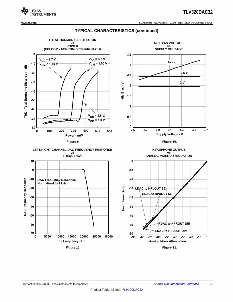
TOTAL HARMONIC DISTORTIONvs MIC BIAS VOLTAGE
POWER vs(HPLCOM - HPRCOM Differential 8.2 Ω) SUPPLY VOLTAGE
Figure 9. Figure 10.
LEFT/RIGHT CHANNEL DAC FREQUENCY RESPONSE HEADPHONE OUTPUTvs vs
FREQUENCY ANALOG MIXER ATTENUATION
Figure 11. Figure 12.
Copyright © 2006–2008, Texas Instruments Incorporated Submit Documentation Feedback 11
Product Folder Link(s): TLV320DAC32
-70
-60
-50
-40
-30
-20
-10
0
-70 -60 -50 -40 -30 -20 -10 0
Digital Volume Control Attenuation
LDAC V Cntrl
RDAC V Cntrl
DA
C O
utp
ut
-160
-140
-120
-100
-80
-60
-40
-20
0
0 2 4 6 8 10 12 14 16 18 20
Frequency - kHz
dB
TLV320DAC32
SLAS506B–NOVEMBER 2006–REVISED DECEMBER 2008........................................................................................................................................ www.ti.com
TYPICAL CHARACTERISTICS (continued)
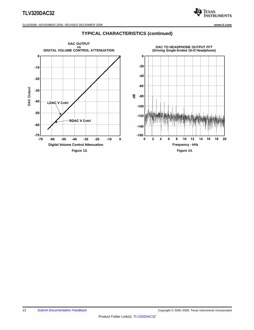
DAC OUTPUTvs DAC TO HEADPHONE OUTPUT FFT
DIGITAL VOLUME CONTROL ATTENUATION (Driving Single-Ended 16-Ω Headphone)
Figure 13. Figure 14.
12 Submit Documentation Feedback Copyright © 2006–2008, Texas Instruments Incorporated
Product Folder Link(s): TLV320DAC32
TYPICAL CIRCUIT CONFIGURATION
AVDD_DAC
DRVDD
DRVDD
A
AVDD
(2.7V-3.6V)
HPLOUT
HPROUT
HPLCOM
HPRCOM/SPKFC
LINEL
0.47 Fm
MICBIAS
LINER
LDO = ON
TLV320DAC32
Multimedia
ProcessorS
CL
SD
A
RE
SE
T
MC
LK
BC
LK
WC
LK
DIN
IOVDD
RR
Line In / FM Tuner
IOVDD
DRVSS
A
D
IOVDD
(1.1-3.3V)
AVSS_DAC
AVSS_DAC
AVSS_DAC
AVSS_DAC
AVSS_DAC
AVSS_DAC
DVDD
IOVSS
DRVSS
LDO_SELECT
8 ohm
8 ohm
0.47 Fm
0.1 Fm
0.1 Fm 1 Fm
1 Fm
0.1 Fm
10 Fm
0.1 Fm 1 Fm
0.1 Fm
1 Fm
TLV320DAC32
www.ti.com........................................................................................................................................ SLAS506B–NOVEMBER 2006–REVISED DECEMBER 2008
TYPICAL CHARACTERISTICS (continued)
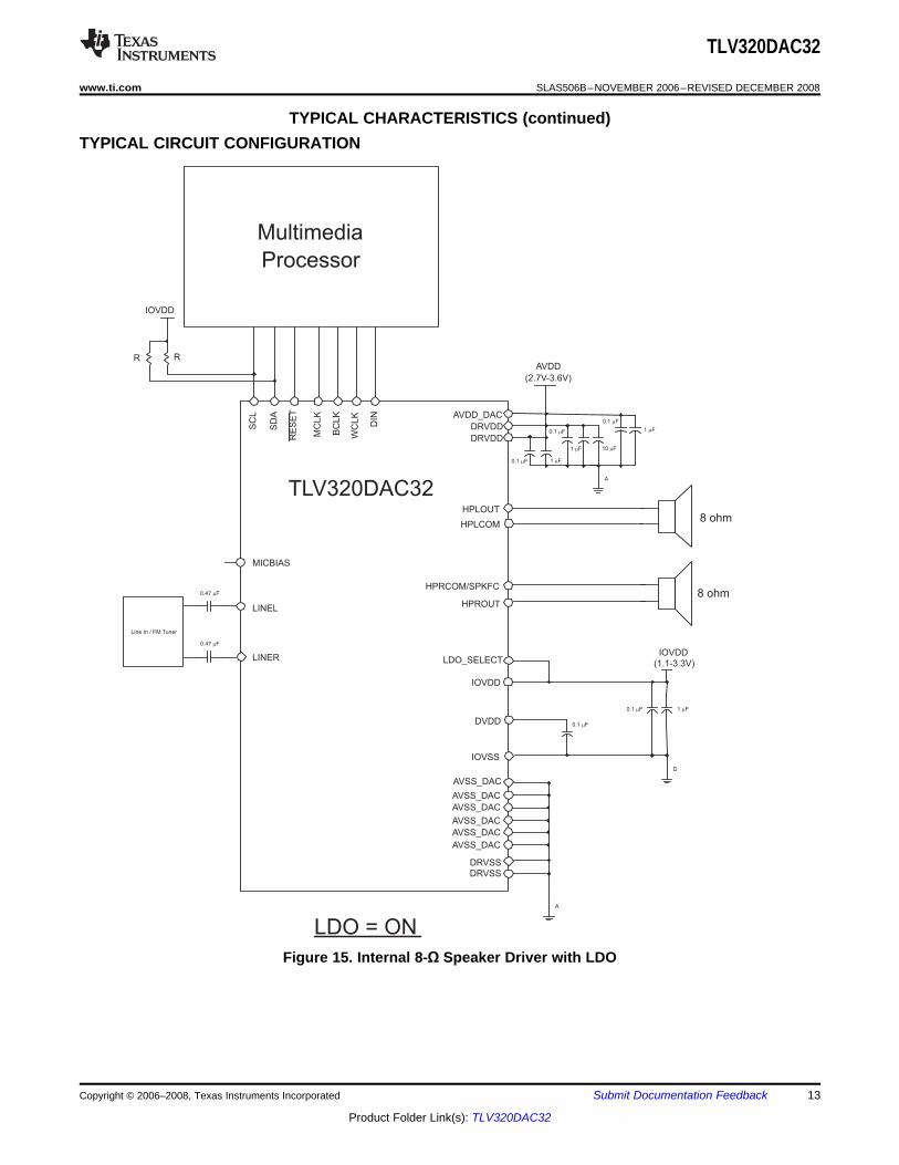
Figure 15. Internal 8-Ω Speaker Driver with LDO
Copyright © 2006–2008, Texas Instruments Incorporated Submit Documentation Feedback 13
Product Folder Link(s): TLV320DAC32
AVDD_DAC
DRVDD
DRVDD
A
AVDD
(2.7V-3.6V)
HPLOUT
HPROUT
HPLCOM
HPRCOM/SPKFC
LINEL
0.47 Fm
MICBIAS
LINER
LDO = OFF
TLV320DAC32
Multimedia
ProcessorS
CL
SD
A
RE
SE
T
MC
LK
BC
LK
WC
LK
DIN
IOVDD
RR
Line In / FM Tuner
IOVDD
DRVSS
A
D
IOVDD
(1.1-3.3V)
AVSS_DAC
AVSS_DAC
AVSS_DAC
AVSS_DAC
AVSS_DAC
AVSS_DAC
DVDD
IOVSS
DRVSS
LDO_SELECT
8 ohm
8 ohm
DVDD
1.525-1.95V
0.47 Fm
0.1 Fm 1 Fm
1 Fm0.1 Fm
1 Fm
0.1 Fm
10 Fm1 Fm
1 Fm
0.1 Fm
0.1 Fm
TLV320DAC32
SLAS506B–NOVEMBER 2006–REVISED DECEMBER 2008........................................................................................................................................ www.ti.com
TYPICAL CHARACTERISTICS (continued)
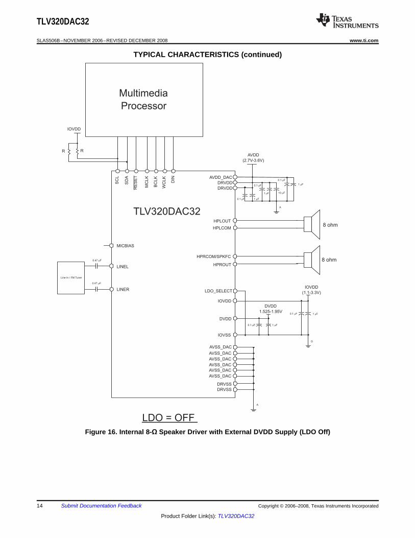
Figure 16. Internal 8-Ω Speaker Driver with External DVDD Supply (LDO Off)
14 Submit Documentation Feedback Copyright © 2006–2008, Texas Instruments Incorporated
Product Folder Link(s): TLV320DAC32
AVDD_DAC
DRVDD
DRVDD
A
AVDD
(2.7V-3.6V)
HPLOUT
HPROUT
HPLCOM
HPRCOM/SPKFC
LINEL
0.47 Fm
MICBIAS
LINER
LDO = ON
TLV320DAC32
Multimedia
ProcessorS
CL
SD
A
RE
SE
T
MC
LK
BC
LK
WC
LK
DIN
IOVDD
RR
Line In / FM Tuner
IOVDD
DRVSS
A
D
IOVDD
(1.1-3.3V)
AVSS_DAC
AVSS_DAC
AVSS_DAC
AVSS_DAC
AVSS_DAC
AVSS_DAC
DVDD
IOVSS
DRVSS
LDO_SELECT
16
ohm
0.47 Fm
0.1 Fm
0.1 Fm 1 Fm
1 Fm
0.1 Fm
10 Fm1 Fm
0.1 Fm
1 Fm0.1 Fm
TLV320DAC32
www.ti.com........................................................................................................................................ SLAS506B–NOVEMBER 2006–REVISED DECEMBER 2008
TYPICAL CHARACTERISTICS (continued)
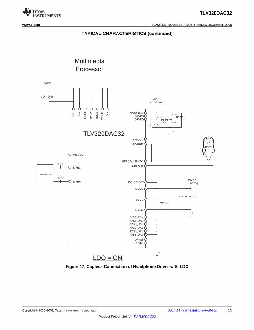
Figure 17. Capless Connection of Headphone Driver with LDO
Copyright © 2006–2008, Texas Instruments Incorporated Submit Documentation Feedback 15
Product Folder Link(s): TLV320DAC32
AVDD_DAC
DRVDD
DRVDD
A
AVDD
(2.7V-3.6V)
HPLOUT
HPROUT
HPLCOM
HPRCOM/SPKFC
LINEL
0.47 Fm
MICBIAS
LINER
LDO = OFF
TLV320DAC32
Multimedia
ProcessorS
CL
SD
A
RE
SE
T
MC
LK
BC
LK
WC
LK
DIN
IOVDD
RR
Line In / FM Tuner
IOVDD
DRVSS
A
D
IOVDD
(1.1-3.3V)
AVSS_DAC
AVSS_DAC
AVSS_DAC
AVSS_DAC
AVSS_DAC
AVSS_DAC
DVDD
IOVSS
DRVSS
LDO_SELECT
16
ohm
DVDD
1.525-1.95V
0.47 Fm
0.1 Fm 1 Fm
0.1 Fm 1 Fm
1 Fm
0.1 Fm
10 Fm1 Fm
0.1 Fm
1 Fm0.1 Fm
TLV320DAC32
SLAS506B–NOVEMBER 2006–REVISED DECEMBER 2008........................................................................................................................................ www.ti.com
TYPICAL CHARACTERISTICS (continued)
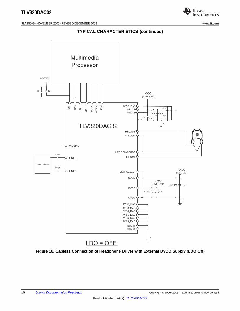
Figure 18. Capless Connection of Headphone Driver with External DVDD Supply (LDO Off)
16 Submit Documentation Feedback Copyright © 2006–2008, Texas Instruments Incorporated
Product Folder Link(s): TLV320DAC32
AVDD_DAC
DRVDD
DRVDD
A
AVDD
(2.7V-3.6V)
HPLOUT
HPROUT
HPLCOM
HPRCOM/SPKFC
LINEL
0.47 Fm
MICBIAS
LINER
LDO = ON
TLV320DAC32
Multimedia
ProcessorS
CL
SD
A
RE
SE
T
MC
LK
BC
LK
WC
LK
DIN
IOVDD
RR
Line In / FM Tuner
IOVDD
DRVSS
A
D
IOVDD
(1.1-3.3V)
AVSS_DAC
AVSS_DAC
AVSS_DAC
AVSS_DAC
AVSS_DAC
AVSS_DAC
DVDD
IOVSS
DRVSS
LDO_SELECT
8 ohm
16
ohm
A
0.47 Fm
0.1 Fm
0.1 Fm 1 Fm
0.1 Fm
1 Fm
10 Fm1 Fm
0.1 Fm
1 Fm0.1 Fm
TLV320DAC32
www.ti.com........................................................................................................................................ SLAS506B–NOVEMBER 2006–REVISED DECEMBER 2008
TYPICAL CHARACTERISTICS (continued)
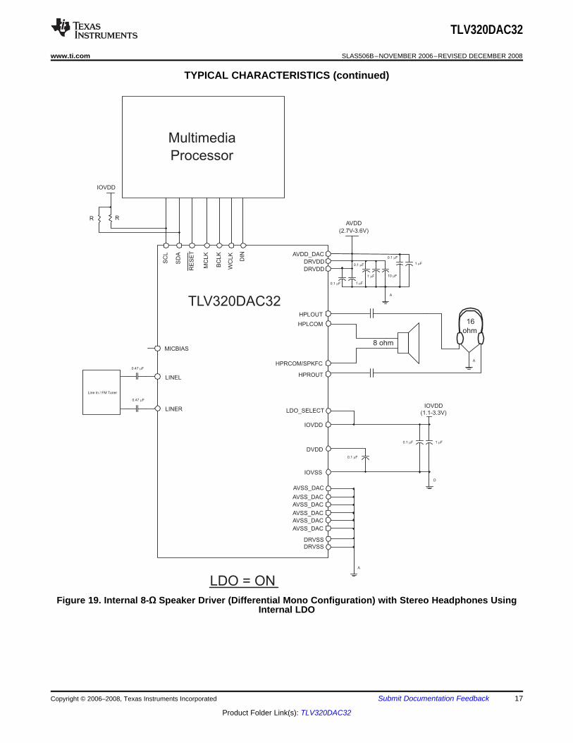
Figure 19. Internal 8-Ω Speaker Driver (Differential Mono Configuration) with Stereo Headphones UsingInternal LDO
Copyright © 2006–2008, Texas Instruments Incorporated Submit Documentation Feedback 17
Product Folder Link(s): TLV320DAC32
AVDD_DAC
DRVDD
DRVDD
A
AVDD
(2.7V-3.6V)
HPLOUT
HPROUT
HPLCOM
HPRCOM/SPKFC
LINEL
0.47 Fm
MICBIAS
LINER
LDO = OFF
TLV320DAC32
Multimedia
ProcessorS
CL
SD
A
RE
SE
T
MC
LK
BC
LK
WC
LK
DIN
IOVDD
RR
Line In / FM Tuner
IOVDD
DRVSS
A
D
IOVDD
(1.1-3.3V)
AVSS_DAC
AVSS_DAC
AVSS_DAC
AVSS_DAC
AVSS_DAC
AVSS_DAC
DVDD
IOVSS
DRVSS
LDO_SELECT
8 ohm
16
ohm
A
DVDD
1.525-1.95V
0.47 Fm
0.1 Fm 1 Fm
0.1 Fm 1 Fm
1 Fm
0.1 Fm
10 Fm1 Fm
0.1 Fm
0.1 Fm 1 Fm
TLV320DAC32
SLAS506B–NOVEMBER 2006–REVISED DECEMBER 2008........................................................................................................................................ www.ti.com
TYPICAL CHARACTERISTICS (continued)
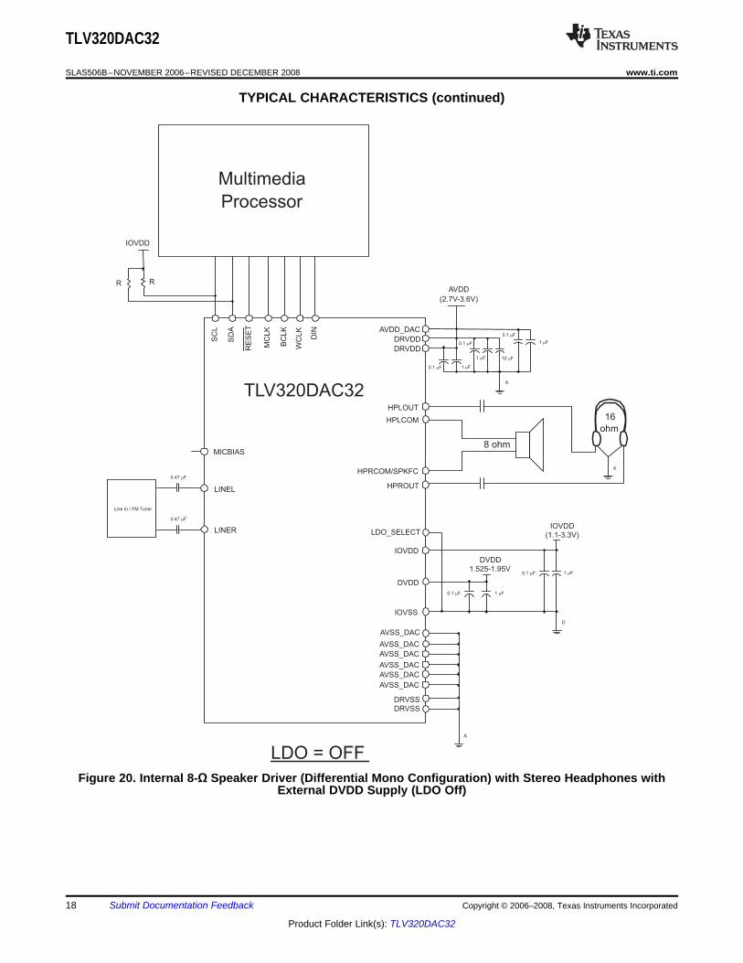
Figure 20. Internal 8-Ω Speaker Driver (Differential Mono Configuration) with Stereo Headphones withExternal DVDD Supply (LDO Off)
18 Submit Documentation Feedback Copyright © 2006–2008, Texas Instruments Incorporated
Product Folder Link(s): TLV320DAC32
OVERVIEW
LDO OPERATION
LDO = ON
TLV320DAC32
IOVDD
D
IOVDD
3.3V
1 Fm0.1 Fm
DVDD
IOVSS
LDO_SELECT
0.1 Fm
TLV320DAC32
www.ti.com........................................................................................................................................ SLAS506B–NOVEMBER 2006–REVISED DECEMBER 2008
The TLV320DAC32 is a highly flexible, low power stereo audio DAC with extensive feature integration, intendedfor application in smartphones, PDAs, and portable computing, communication, and entertainment applications.Available in a 5x5mm 32-lead QFN, the product integrates a host of features to reduce cost, board space, andpower consumption in space-constrained, battery powered portable applications.
The TLV320DAC32 consists of the following blocks:• Stereo audio multi-bit delta-sigma DAC (8 kHz – 96 kHz)• Programmable digital audio effects processing (3-D, bass, treble, mid-range, EQ, de-emphasis)• Two analog audio input pins• Four high-power audio output drivers (headphone/speaker drive capability)• Fully programmable PLL• Programmable voltage level for microphone biasing• Headphone/headset jack detection with interrupt• Selectable internal LDO regulator for systems that only have +3.3V power available.
The I2C interface supports both standard and fast communication modes.
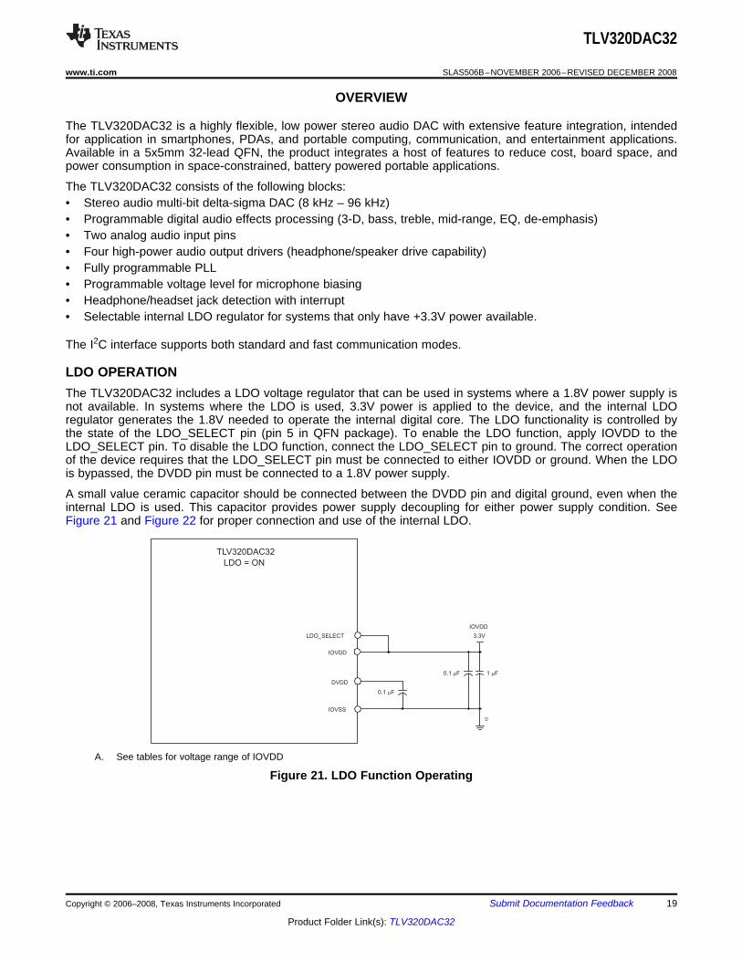
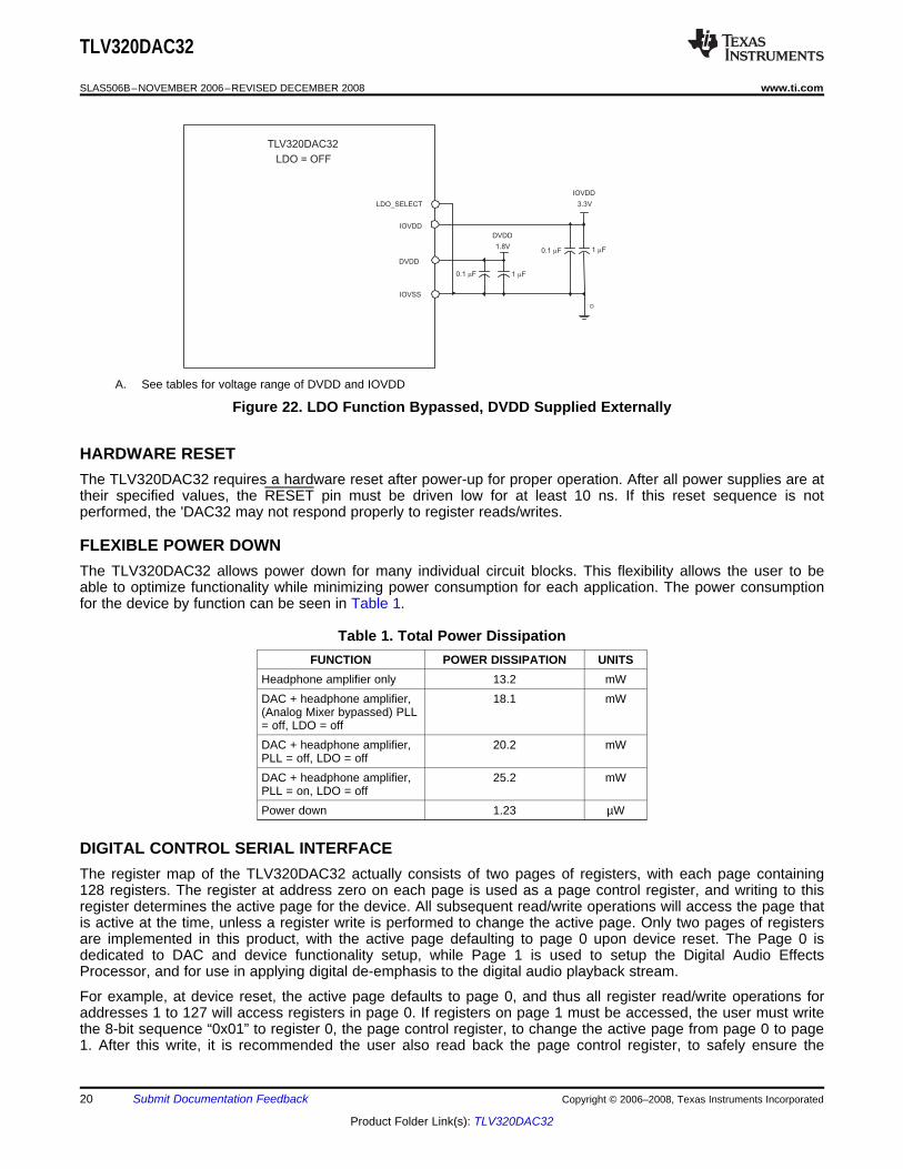
The TLV320DAC32 includes a LDO voltage regulator that can be used in systems where a 1.8V power supply isnot available. In systems where the LDO is used, 3.3V power is applied to the device, and the internal LDOregulator generates the 1.8V needed to operate the internal digital core. The LDO functionality is controlled bythe state of the LDO_SELECT pin (pin 5 in QFN package). To enable the LDO function, apply IOVDD to theLDO_SELECT pin. To disable the LDO function, connect the LDO_SELECT pin to ground. The correct operationof the device requires that the LDO_SELECT pin must be connected to either IOVDD or ground. When the LDOis bypassed, the DVDD pin must be connected to a 1.8V power supply.
A small value ceramic capacitor should be connected between the DVDD pin and digital ground, even when theinternal LDO is used. This capacitor provides power supply decoupling for either power supply condition. SeeFigure 21 and Figure 22 for proper connection and use of the internal LDO.
A. See tables for voltage range of IOVDD
Figure 21. LDO Function Operating
Copyright © 2006–2008, Texas Instruments Incorporated Submit Documentation Feedback 19
Product Folder Link(s): TLV320DAC32
LDO = OFF
TLV320DAC32
IOVDD
D
IOVDD
3.3V
1 Fm0.1 Fm
DVDD
IOVSS
LDO_SELECT
DVDD
1.8V
1 Fm0.1 Fm
HARDWARE RESET
FLEXIBLE POWER DOWN
DIGITAL CONTROL SERIAL INTERFACE
TLV320DAC32
SLAS506B–NOVEMBER 2006–REVISED DECEMBER 2008........................................................................................................................................ www.ti.com
A. See tables for voltage range of DVDD and IOVDD
Figure 22. LDO Function Bypassed, DVDD Supplied Externally
The TLV320DAC32 requires a hardware reset after power-up for proper operation. After all power supplies are attheir specified values, the RESET pin must be driven low for at least 10 ns. If this reset sequence is notperformed, the 'DAC32 may not respond properly to register reads/writes.
The TLV320DAC32 allows power down for many individual circuit blocks. This flexibility allows the user to beable to optimize functionality while minimizing power consumption for each application. The power consumptionfor the device by function can be seen in Table 1.
Table 1. Total Power DissipationFUNCTION POWER DISSIPATION UNITS
Headphone amplifier only 13.2 mWDAC + headphone amplifier, 18.1 mW(Analog Mixer bypassed) PLL= off, LDO = offDAC + headphone amplifier, 20.2 mWPLL = off, LDO = offDAC + headphone amplifier, 25.2 mWPLL = on, LDO = offPower down 1.23 µW
The register map of the TLV320DAC32 actually consists of two pages of registers, with each page containing128 registers. The register at address zero on each page is used as a page control register, and writing to thisregister determines the active page for the device. All subsequent read/write operations will access the page thatis active at the time, unless a register write is performed to change the active page. Only two pages of registersare implemented in this product, with the active page defaulting to page 0 upon device reset. The Page 0 isdedicated to DAC and device functionality setup, while Page 1 is used to setup the Digital Audio EffectsProcessor, and for use in applying digital de-emphasis to the digital audio playback stream.
For example, at device reset, the active page defaults to page 0, and thus all register read/write operations foraddresses 1 to 127 will access registers in page 0. If registers on page 1 must be accessed, the user must writethe 8-bit sequence “0x01” to register 0, the page control register, to change the active page from page 0 to page1. After this write, it is recommended the user also read back the page control register, to safely ensure the
20 Submit Documentation Feedback Copyright © 2006–2008, Texas Instruments Incorporated
Product Folder Link(s): TLV320DAC32
I2C CONTROL MODE
SDA
SCL
tHD-STA
0.9 s³ m
tSU-STO
0.9 s³ m
P S
tSU-STA
0.9 s³ m
Sr
tHD-STA
0.9 s³ m
S
T0114-02
TLV320DAC32
www.ti.com........................................................................................................................................ SLAS506B–NOVEMBER 2006–REVISED DECEMBER 2008
change in page control has occurred properly. Future read/write operations to addresses 1 to 127 will nowaccess registers in page 1. When page 0 registers must be accessed again, the user writes the 8-bit sequence“0x00” to register 0, the page control register, to change the active page back to page 0. After a recommendedread of the page control register, all further read/write operations to addresses 1 to 127 will now access page 0registers again.
It is considered to be a best practice, that when writing to PAGE 1, all five of the digital filter’s coefficients of theBi-Quad structure be updated to the new values before resuming digital audio playback.
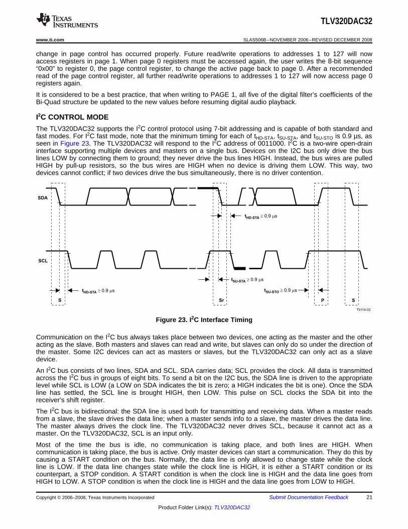
The TLV320DAC32 supports the I2C control protocol using 7-bit addressing and is capable of both standard andfast modes. For I2C fast mode, note that the minimum timing for each of tHD-STA, tSU-STA, and tSU-STO is 0.9 µs, asseen in Figure 23. The TLV320DAC32 will respond to the I2C address of 0011000. I2C is a two-wire open-draininterface supporting multiple devices and masters on a single bus. Devices on the I2C bus only drive the buslines LOW by connecting them to ground; they never drive the bus lines HIGH. Instead, the bus wires are pulledHIGH by pull-up resistors, so the bus wires are HIGH when no device is driving them LOW. This way, twodevices cannot conflict; if two devices drive the bus simultaneously, there is no driver contention.
Figure 23. I2C Interface Timing
Communication on the I2C bus always takes place between two devices, one acting as the master and the otheracting as the slave. Both masters and slaves can read and write, but slaves can only do so under the direction ofthe master. Some I2C devices can act as masters or slaves, but the TLV320DAC32 can only act as a slavedevice.
An I2C bus consists of two lines, SDA and SCL. SDA carries data; SCL provides the clock. All data is transmittedacross the I2C bus in groups of eight bits. To send a bit on the I2C bus, the SDA line is driven to the appropriatelevel while SCL is LOW (a LOW on SDA indicates the bit is zero; a HIGH indicates the bit is one). Once the SDAline has settled, the SCL line is brought HIGH, then LOW. This pulse on SCL clocks the SDA bit into thereceiver’s shift register.
The I2C bus is bidirectional: the SDA line is used both for transmitting and receiving data. When a master readsfrom a slave, the slave drives the data line; when a master sends info to a slave, the master drives the data line.The master always drives the clock line. The TLV320DAC32 never drives SCL, because it cannot act as amaster. On the TLV320DAC32, SCL is an input only.
Most of the time the bus is idle, no communication is taking place, and both lines are HIGH. Whencommunication is taking place, the bus is active. Only master devices can start a communication. They do this bycausing a START condition on the bus. Normally, the data line is only allowed to change state while the clockline is LOW. If the data line changes state while the clock line is HIGH, it is either a START condition or itscounterpart, a STOP condition. A START condition is when the clock line is HIGH and the data line goes fromHIGH to LOW. A STOP condition is when the clock line is HIGH and the data line goes from LOW to HIGH.
Copyright © 2006–2008, Texas Instruments Incorporated Submit Documentation Feedback 21
Product Folder Link(s): TLV320DAC32
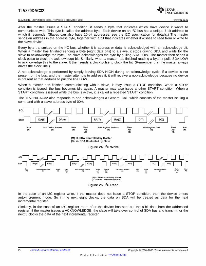
DA(6) DA(0) RA(7) RA(0) D(7) D(0)
Start
(M)
7-bit Device Address
(M)
Write
(M)
Slave
Ack(S)
8-bit Register Address
(M)
Slave
Ack(S)
8-bit Register Data
(M)
Stop
(M)
Slave
Ack(S)
SDA
SCL
(M) => SDA Controlled by Master
(S) => SDA Controlled by Slave
DA(6) DA(0) RA(7) RA(0)
Start
(M)7-bit Device Address
(M)
Write
(M)
SlaveAck
(S)
8-bit Register Address
(M)
SlaveAck
(S)
SDA
SCL
DA(6) DA(0)
7-bit Device Address
(M)
Read
(M)
SlaveAck
(S)
D(7) D(0)
8-bit Register Data
(S)
Stop
(M)
MasterNo Ack
(M)
RepeatStart
(M)
(M) => SDA Controlled by Master
(S) => SDA Controlled by Slave
TLV320DAC32
SLAS506B–NOVEMBER 2006–REVISED DECEMBER 2008........................................................................................................................................ www.ti.com
After the master issues a START condition, it sends a byte that indicates which slave device it wants tocommunicate with. This byte is called the address byte. Each device on an I2C bus has a unique 7-bit address towhich it responds. (Slaves can also have 10-bit addresses; see the I2C specification for details.) The mastersends an address in the address byte, together with a bit that indicates whether it wishes to read from or write tothe slave device.
Every byte transmitted on the I2C bus, whether it is address or data, is acknowledged with an acknowledge bit.When a master has finished sending a byte (eight data bits) to a slave, it stops driving SDA and waits for theslave to acknowledge the byte. The slave acknowledges the byte by pulling SDA LOW. The master then sends aclock pulse to clock the acknowledge bit. Similarly, when a master has finished reading a byte, it pulls SDA LOWto acknowledge this to the slave. It then sends a clock pulse to clock the bit. (Remember that the master alwaysdrives the clock line.)
A not-acknowledge is performed by simply leaving SDA HIGH during an acknowledge cycle. If a device is notpresent on the bus, and the master attempts to address it, it will receive a not−acknowledge because no deviceis present at that address to pull the line LOW.
When a master has finished communicating with a slave, it may issue a STOP condition. When a STOPcondition is issued, the bus becomes idle again. A master may also issue another START condition. When aSTART condition is issued while the bus is active, it is called a repeated START condition.
The TLV320DAC32 also responds to and acknowledges a General Call, which consists of the master issuing acommand with a slave address byte of 00H.
Figure 24. I2C Write
Figure 25. I2C Read
In the case of an I2C register write, if the master does not issue a STOP condition, then the device entersauto-increment mode. So in the next eight clocks, the data on SDA will be treated as data for the nextincremental register.
Similarly, in the case of an I2C register read, after the device has sent out the 8-bit data from the addressedregister, if the master issues a ACKNOWLEDGE, the slave will take over control of SDA bus and transmit for thenext 8 clocks the data of the next incremental register.
22 Submit Documentation Feedback Copyright © 2006–2008, Texas Instruments Incorporated
Product Folder Link(s): TLV320DAC32
DIGITAL AUDIO DATA SERIAL INTERFACE
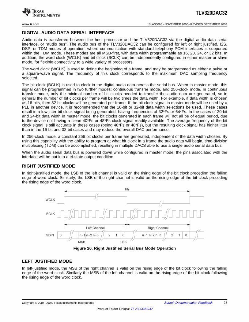
RIGHT JUSTIFIED MODE
BCLK
WCLK
SDIN 1 00 1 0
1/fs
LSBMSB
Left Channel Right Channel
2 2n−1 n−3n−2 n−1 n−3n−2
LEFT JUSTIFIED MODE
TLV320DAC32
www.ti.com........................................................................................................................................ SLAS506B–NOVEMBER 2006–REVISED DECEMBER 2008
Audio data is transferred between the host processor and the TLV320DAC32 via the digital audio data serialinterface, or “audio bus”. The audio bus of the TLV320DAC32 can be configured for left or right justified, I2S,DSP, or TDM modes of operation, where communication with standard telephony PCM interfaces is supportedwithin the TDM mode. These modes are all MSB-first, with data width programmable as 16, 20, 24, or 32 bits. Inaddition, the word clock (WCLK) and bit clock (BCLK) can be independently configured in either master or slavemode, for flexible connectivity to a wide variety of processors.
The word clock (WCLK) is used to define the beginning of a frame, and may be programmed as either a pulse ora square-wave signal. The frequency of this clock corresponds to the maximum DAC sampling frequencyselected.
The bit clock (BCLK) is used to clock in the digital audio data across the serial bus. When in master mode, thissignal can be programmed in two further modes: continuous transfer mode, and 256-clock mode. In continuoustransfer mode, only the minimal number of bit clocks needed to transfer the audio data are generated, so ingeneral the number of bit clocks per frame will be two times the data width. For example, if data width is chosenas 16-bits, then 32 bit clocks will be generated per frame. If the bit clock signal in master mode will be used by aPLL in another device, it is recommended that the 16-bit or 32-bit data width selections be used. These casesresult in a low jitter bit clock signal being generated, having frequencies of 32*Fs or 64*Fs. In the cases of 20-bitand 24-bit data width in master mode, the bit clocks generated in each frame will not all be of equal period, dueto the device not having a clean 40*Fs or 48*Fs clock signal readily available. The average frequency of the bitclock signal is still accurate in these cases (being 40*Fs or 48*Fs), but the resulting clock signal has higher jitterthan in the 16-bit and 32-bit cases and may reduce the overall DAC performance.
In 256-clock mode, a constant 256 bit clocks per frame are generated, independent of the data width chosen. Byusing this capability with the ability to program at what bit clock in a frame the audio data will begin, time-divisionmultiplexing (TDM) can be accomplished, resulting in multiple DACS able to use a single audio serial data bus.
When the audio serial data bus is powered down while configured in master mode, the pins associated with theinterface will be put into a tri-state output condition.
In right-justified mode, the LSB of the left channel is valid on the rising edge of the bit clock preceding the fallingedge of word clock. Similarly, the LSB of the right channel is valid on the rising edge of the bit clock precedingthe rising edge of the word clock.
Figure 26. Right Justified Serial Bus Mode Operation
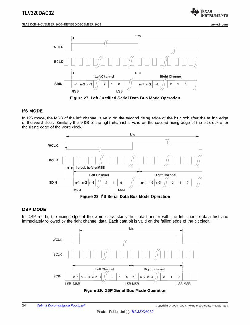
In left-justified mode, the MSB of the right channel is valid on the rising edge of the bit clock following the fallingedge of the word clock. Similarly the MSB of the left channel is valid on the rising edge of the bit clock followingthe rising edge of the word clock.
Copyright © 2006–2008, Texas Instruments Incorporated Submit Documentation Feedback 23
Product Folder Link(s): TLV320DAC32
n-1 n-2 n-3 n-1 n-2 n-3
I2S MODE
n-1 n-2 n-3 n-1 n-2 n-3
DSP MODE
BCLK
WCLK
SDIN n−2 n−3 1 0 n−1 n−2 1 0
1/fs
LSBMSB
Left Channel Right Channel
n−1
MSB LSB
n−4 2 n−3 2
MSBLSB
TLV320DAC32
SLAS506B–NOVEMBER 2006–REVISED DECEMBER 2008........................................................................................................................................ www.ti.com
Figure 27. Left Justified Serial Data Bus Mode Operation
In I2S mode, the MSB of the left channel is valid on the second rising edge of the bit clock after the falling edgeof the word clock. Similarly the MSB of the right channel is valid on the second rising edge of the bit clock afterthe rising edge of the word clock.
Figure 28. I2S Serial Data Bus Mode Operation
In DSP mode, the rising edge of the word clock starts the data transfer with the left channel data first andimmediately followed by the right channel data. Each data bit is valid on the falling edge of the bit clock.
Figure 29. DSP Serial Bus Mode Operation
24 Submit Documentation Feedback Copyright © 2006–2008, Texas Instruments Incorporated
Product Folder Link(s): TLV320DAC32
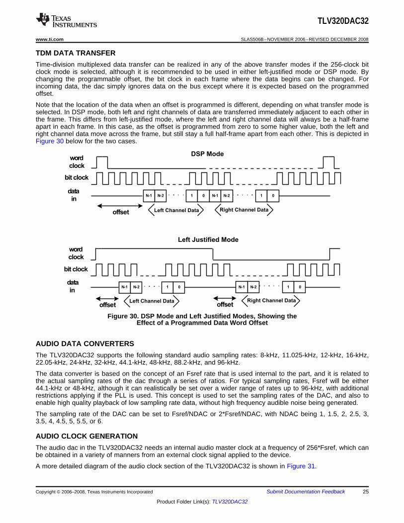
TDM DATA TRANSFER
N-1 N-2 1 0 N-1 N-2 1 0
wordclock
bit clock
datain
Right Channel Data
Right Channel Data
Left Channel Data
Left Channel Data
N-1 N-2 1 0 N-1 N-2 1 0
wordclock
bit clock
datain
DSP Mode
Left Justified Mode
offset
offset
offset
AUDIO DATA CONVERTERS
AUDIO CLOCK GENERATION
TLV320DAC32
www.ti.com........................................................................................................................................ SLAS506B–NOVEMBER 2006–REVISED DECEMBER 2008
Time-division multiplexed data transfer can be realized in any of the above transfer modes if the 256-clock bitclock mode is selected, although it is recommended to be used in either left-justified mode or DSP mode. Bychanging the programmable offset, the bit clock in each frame where the data begins can be changed. Forincoming data, the dac simply ignores data on the bus except where it is expected based on the programmedoffset.
Note that the location of the data when an offset is programmed is different, depending on what transfer mode isselected. In DSP mode, both left and right channels of data are transferred immediately adjacent to each other inthe frame. This differs from left-justified mode, where the left and right channel data will always be a half-frameapart in each frame. In this case, as the offset is programmed from zero to some higher value, both the left andright channel data move across the frame, but still stay a full half-frame apart from each other. This is depicted inFigure 30 below for the two cases.
Figure 30. DSP Mode and Left Justified Modes, Showing theEffect of a Programmed Data Word Offset
The TLV320DAC32 supports the following standard audio sampling rates: 8-kHz, 11.025-kHz, 12-kHz, 16-kHz,22.05-kHz, 24-kHz, 32-kHz, 44.1-kHz, 48-kHz, 88.2-kHz, and 96-kHz.
The data converter is based on the concept of an Fsref rate that is used internal to the part, and it is related tothe actual sampling rates of the dac through a series of ratios. For typical sampling rates, Fsref will be either44.1-kHz or 48-kHz, although it can realistically be set over a wider range of rates up to 96-kHz, with additionalrestrictions applying if the PLL is used. This concept is used to set the sampling rates of the DAC, and also toenable high quality playback of low sampling rate data, without high frequency audible noise being generated.
The sampling rate of the DAC can be set to Fsref/NDAC or 2*Fsref/NDAC, with NDAC being 1, 1.5, 2, 2.5, 3,3.5, 4, 4.5, 5, 5.5, or 6.
The audio dac in the TLV320DAC32 needs an internal audio master clock at a frequency of 256*Fsref, which canbe obtained in a variety of manners from an external clock signal applied to the device.
A more detailed diagram of the audio clock section of the TLV320DAC32 is shown in Figure 31.
Copyright © 2006–2008, Texas Instruments Incorporated Submit Documentation Feedback 25
Product Folder Link(s): TLV320DAC32
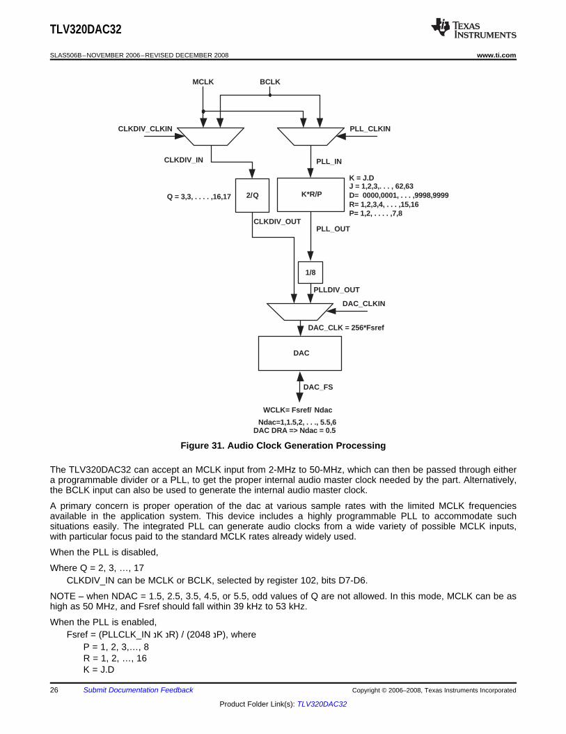
2/Q
PLL_CLKIN
DAC
DAC_CLKIN
PLL_OUT
K = J.DJ = 1,2,3,. . . , 62,63D= 0000,0001, . . . ,9998,9999R= 1,2,3,4, . . . ,15,16P= 1,2, . . . . ,7,8
MCLK BCLK
CLKDIV_IN PLL_IN
WCLK= Fsref/ Ndac
DAC_FS
Ndac=1,1.5,2, . . ., 5.5,6DAC DRA => Ndac = 0.5
DAC_CLK = 256*Fsref
CLKDIV_OUT
1/8
PLLDIV_OUT
CLKDIV_CLKIN
Q = 3,3, . . . . ,16,17 K*R/P
TLV320DAC32
SLAS506B–NOVEMBER 2006–REVISED DECEMBER 2008........................................................................................................................................ www.ti.com
Figure 31. Audio Clock Generation Processing
The TLV320DAC32 can accept an MCLK input from 2-MHz to 50-MHz, which can then be passed through eithera programmable divider or a PLL, to get the proper internal audio master clock needed by the part. Alternatively,the BCLK input can also be used to generate the internal audio master clock.
A primary concern is proper operation of the dac at various sample rates with the limited MCLK frequenciesavailable in the application system. This device includes a highly programmable PLL to accommodate suchsituations easily. The integrated PLL can generate audio clocks from a wide variety of possible MCLK inputs,with particular focus paid to the standard MCLK rates already widely used.
When the PLL is disabled,
Where Q = 2, 3, …, 17CLKDIV_IN can be MCLK or BCLK, selected by register 102, bits D7-D6.
NOTE – when NDAC = 1.5, 2.5, 3.5, 4.5, or 5.5, odd values of Q are not allowed. In this mode, MCLK can be ashigh as 50 MHz, and Fsref should fall within 39 kHz to 53 kHz.
When the PLL is enabled,Fsref = (PLLCLK_IN Kנ (Rנ / (2048 ,(Pנ where
P = 1, 2, 3,…, 8R = 1, 2, …, 16K = J.D
26 Submit Documentation Feedback Copyright © 2006–2008, Texas Instruments Incorporated
Product Folder Link(s): TLV320DAC32
TLV320DAC32
www.ti.com........................................................................................................................................ SLAS506B–NOVEMBER 2006–REVISED DECEMBER 2008
J = 1, 2, 3, …, 63D = 0000, 0001, 0002, 0003, …, 9998, 9999PLLCLK_IN can be MCLK or BCLK, selected by Page 0, register 102, bits D5-D4
P, R, J, and D are register programmable. J is the integer portion of K (the numbers to the left of the decimalpoint), while D is the fractional portion of K (the numbers to the right of the decimal point, assuming four digits ofprecision).
Examples:If K = 8.5, then J = 8, D = 5000If K = 7.12, then J = 7, D = 1200If K = 14.03, then J = 14, D = 0300If K = 6.0004, then J = 6, D = 0004
When the PLL is enabled and D = 0000, the following conditions must be satisfied to meet specifiedperformance:
2 MHz ≤ ( PLLCLK_IN / P ) ≤ 20 MHz80 MHz ≤ (PLLCLK _IN Kנ Rנ / P ) ≤ 110 MHz4 ≤ J ≤ 55
When the PLL is enabled and D≠0000, the following conditions must be satisfied to meet specified performance:10 MHz ≤ PLLCLK _IN / P ≤ 20 MHz80 MHz ≤ PLLCLK _IN Kנ Rנ / P ≤ 110 MHz4 ≤ J ≤ 11R = 1
Example:MCLK = 12 MHz and Fsref = 44.1 kHzSelect P = 1, R = 1, K = 7.5264, which results in J = 7, D = 5264
Example:MCLK = 12 MHz and Fsref = 48.0 kHzSelect P = 1, R = 1, K = 8.192, which results in J = 8, D = 1920
The table below lists several example cases of typical MCLK rates and how to program the PLL to achieve Fsref= 44.1 kHz or 48 kHz.Fsref = 44.1 kHzMCLK (MHz) P R J D ACHIEVED FSREF % ERROR2.8224 1 1 32 0 44100.00 0.00005.6448 1 1 16 0 44100.00 0.000012.0 1 1 7 5264 44100.00 0.000013.0 1 1 6 9474 44099.71 0.000716.0 1 1 5 6448 44100.00 0.000019.2 1 1 4 7040 44100.00 0.000019.68 1 1 4 5893 44100.30 –0.000748.0 4 1 7 5264 44100.00 0.0000Fsref = 48 kHzMCLK (MHz) P R J D ACHIEVED FSREF % ERROR2.048 1 1 48 0 48000.00 0.00003.072 1 1 32 0 48000.00 0.00004.096 1 1 24 0 48000.00 0.00006.144 1 1 16 0 48000.00 0.00008.192 1 1 12 0 48000.00 0.000012.0 1 1 8 1920 48000.00 0.000013.0 1 1 7 5618 47999.71 0.0006
Copyright © 2006–2008, Texas Instruments Incorporated Submit Documentation Feedback 27
Product Folder Link(s): TLV320DAC32
STEREO AUDIO DAC
DIGITAL AUDIO PROCESSING
H(z) N0 N1 z1
32768 D1 z1 (1)
N0 2 N1 z1 N2 z2
32768 2 D1 z1 D2 z2 N3 2 N4 z1 N5 z2
32768 2 D4 z1 D5 z2
(2)
TLV320DAC32
SLAS506B–NOVEMBER 2006–REVISED DECEMBER 2008........................................................................................................................................ www.ti.com
16.0 1 1 6 1440 48000.00 0.000019.2 1 1 5 1200 48000.00 0.000019.68 1 1 4 9951 47999.79 0.000448.0 4 1 8 1920 48000.00 0.0000
The TLV320DAC32 includes a stereo audio DAC supporting sampling rates from 8-kHz to 96-kHz. Each channelof the stereo audio DAC consists of a digital audio processing block, a digital interpolation filter, multi-bit digitaldelta-sigma modulator, and an analog reconstruction filter. The DAC is designed to provide enhancedperformance at low sampling rates through increased oversampling and image filtering, thereby keepingquantization noise generated within the delta-sigma modulator and signal images strongly suppressed within theaudio band to beyond 20-kHz. This is realized by keeping the upsampled rate constant at 128 x Fsref andchanging the oversampling ratio as the input sample rate is changed. For an Fsref of 48-kHz, the digitaldelta-sigma modulator always operates at a rate of 6.144-MHz. This ensures that quantization noise generatedwithin the delta-sigma modulator stays low within the frequency band below 20-kHz at all sample rates. Similarly,for an Fsref rate of 44.1-kHz, the digital delta-sigma modulator always operates at a rate of 5.6448-MHz.
The following restrictions apply in the case when the PLL is powered down and double-rate audio mode isenabled in the DAC.
Allowed Q values = 4, 8, 9, 12, 16Q values where equivalent Fsref can be achieved by turning on PLLQ = 5, 6, 7 (set P = 5 / 6 / 7 and K = 16.0 and PLL enabled)Q = 10, 14 (set P = 5, 7 and K = 8.0 and PLL enabled)
The DAC channel consists of optional filters for de-emphasis and bass, treble, midrange level adjustment,speaker equalization, and 3-D effects processing. The de-emphasis function is implemented by a programmabledigital filter block with fully programmable coefficients (see Page-1/Reg-21-26 for left channel, Page-1/Reg-47-52for right channel). If de-emphasis is not required in a particular application, this programmable filter block can beused for some other purpose. The de-emphasis filter transfer function is given by:
where the N0, N1, and D1 coefficients are fully programmable individually for each channel. The coefficients thatshould be loaded to implement standard de-emphasis filters are given in Table 1.
Table 2. De-Emphasis Coefficients for Common Audio Sampling RatesSAMPLING FREQUENCY N0 N1 D1
32-kHz 16950 –1220 1703744.1-kHz 15091 –2877 2055548-kHz (1) 14677 –3283 21374
(1) The 48-kHz coefficients listed above are used as the default values.
In addition to the de-emphasis filter block, the DAC digital effects processing includes a fourth order digital IIRfilter with programmable coefficients (one set per channel). This filter is implemented as cascade of two biquadsections with frequency response given by:
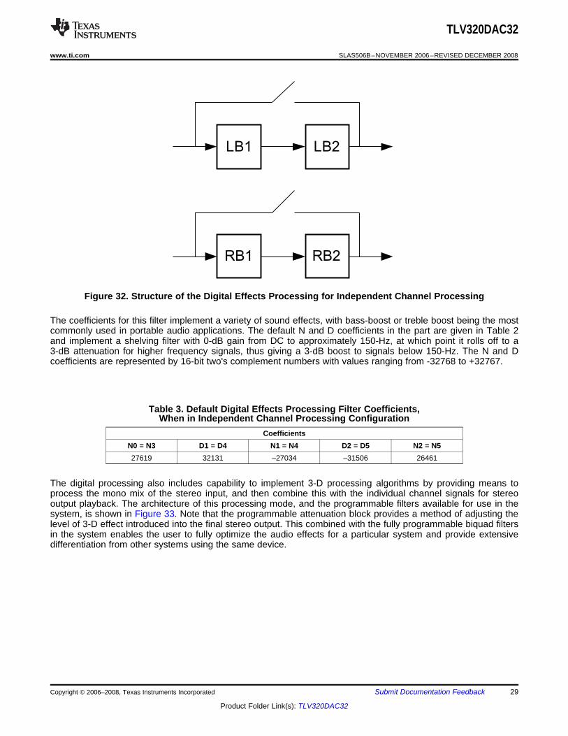
The N and D coefficients are fully programmable, and the entire filter can be enabled or bypassed. The structureof the filtering when configured for independent channel processing is shown below in Figure 32, with LB1corresponding to the first left-channel biquad filter using coefficients N0, N1, N2, D1, and D2. LB2 similarlycorresponds to the second left-channel biquad filter using coefficients N3, N4, N5, D4, and D5. The RB1 andRB2 filters refer to the first and second right-channel biquad filters, respectively.
28 Submit Documentation Feedback Copyright © 2006–2008, Texas Instruments Incorporated
Product Folder Link(s): TLV320DAC32
LB1 LB2
RB1 RB2
TLV320DAC32
www.ti.com........................................................................................................................................ SLAS506B–NOVEMBER 2006–REVISED DECEMBER 2008
Figure 32. Structure of the Digital Effects Processing for Independent Channel Processing
The coefficients for this filter implement a variety of sound effects, with bass-boost or treble boost being the mostcommonly used in portable audio applications. The default N and D coefficients in the part are given in Table 2and implement a shelving filter with 0-dB gain from DC to approximately 150-Hz, at which point it rolls off to a3-dB attenuation for higher frequency signals, thus giving a 3-dB boost to signals below 150-Hz. The N and Dcoefficients are represented by 16-bit two's complement numbers with values ranging from -32768 to +32767.
Table 3. Default Digital Effects Processing Filter Coefficients,When in Independent Channel Processing Configuration
CoefficientsN0 = N3 D1 = D4 N1 = N4 D2 = D5 N2 = N527619 32131 –27034 –31506 26461
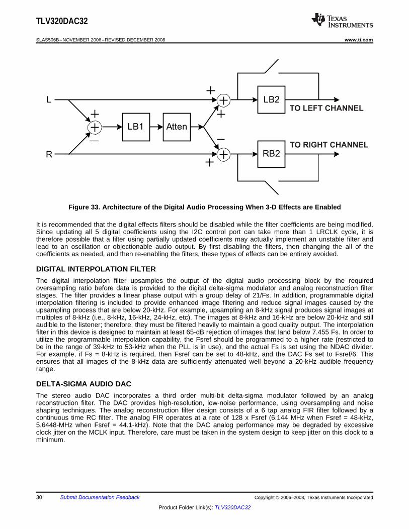
The digital processing also includes capability to implement 3-D processing algorithms by providing means toprocess the mono mix of the stereo input, and then combine this with the individual channel signals for stereooutput playback. The architecture of this processing mode, and the programmable filters available for use in thesystem, is shown in Figure 33. Note that the programmable attenuation block provides a method of adjusting thelevel of 3-D effect introduced into the final stereo output. This combined with the fully programmable biquad filtersin the system enables the user to fully optimize the audio effects for a particular system and provide extensivedifferentiation from other systems using the same device.
Copyright © 2006–2008, Texas Instruments Incorporated Submit Documentation Feedback 29
Product Folder Link(s): TLV320DAC32
LB1
RB2
Atten
LB2L
R
TOLEFTCHANNEL
TO RIGHT CHANNEL
TO LEFT CHANNEL
TO RIGHT CHANNEL
DIGITAL INTERPOLATION FILTER
DELTA-SIGMA AUDIO DAC
TLV320DAC32
SLAS506B–NOVEMBER 2006–REVISED DECEMBER 2008........................................................................................................................................ www.ti.com
Figure 33. Architecture of the Digital Audio Processing When 3-D Effects are Enabled
It is recommended that the digital effects filters should be disabled while the filter coefficients are being modified.Since updating all 5 digital coefficients using the I2C control port can take more than 1 LRCLK cycle, it istherefore possible that a filter using partially updated coefficients may actually implement an unstable filter andlead to an oscillation or objectionable audio output. By first disabling the filters, then changing the all of thecoefficients as needed, and then re-enabling the filters, these types of effects can be entirely avoided.
The digital interpolation filter upsamples the output of the digital audio processing block by the requiredoversampling ratio before data is provided to the digital delta-sigma modulator and analog reconstruction filterstages. The filter provides a linear phase output with a group delay of 21/Fs. In addition, programmable digitalinterpolation filtering is included to provide enhanced image filtering and reduce signal images caused by theupsampling process that are below 20-kHz. For example, upsampling an 8-kHz signal produces signal images atmultiples of 8-kHz (i.e., 8-kHz, 16-kHz, 24-kHz, etc). The images at 8-kHz and 16-kHz are below 20-kHz and stillaudible to the listener; therefore, they must be filtered heavily to maintain a good quality output. The interpolationfilter in this device is designed to maintain at least 65-dB rejection of images that land below 7.455 Fs. In order toutilize the programmable interpolation capability, the Fsref should be programmed to a higher rate (restricted tobe in the range of 39-kHz to 53-kHz when the PLL is in use), and the actual Fs is set using the NDAC divider.For example, if Fs = 8-kHz is required, then Fsref can be set to 48-kHz, and the DAC Fs set to Fsref/6. Thisensures that all images of the 8-kHz data are sufficiently attenuated well beyond a 20-kHz audible frequencyrange.
The stereo audio DAC incorporates a third order multi-bit delta-sigma modulator followed by an analogreconstruction filter. The DAC provides high-resolution, low-noise performance, using oversampling and noiseshaping techniques. The analog reconstruction filter design consists of a 6 tap analog FIR filter followed by acontinuous time RC filter. The analog FIR operates at a rate of 128 x Fsref (6.144 MHz when Fsref = 48-kHz,5.6448-MHz when Fsref = 44.1-kHz). Note that the DAC analog performance may be degraded by excessiveclock jitter on the MCLK input. Therefore, care must be taken in the system design to keep jitter on this clock to aminimum.
30 Submit Documentation Feedback Copyright © 2006–2008, Texas Instruments Incorporated
Product Folder Link(s): TLV320DAC32
AUDIO DAC DIGITAL VOLUME CONTROL
AUDIO DAC COMMON-MODE ADJUSTMENT
AUDIO DAC POWER CONTROL
TLV320DAC32
www.ti.com........................................................................................................................................ SLAS506B–NOVEMBER 2006–REVISED DECEMBER 2008
The audio DAC includes a digital volume control block which implements a programmable digital gain. Thevolume level can be varied from 0-dB to –63.5-dB in 0.5-dB steps, in addition to a mute bit, independently foreach channel. The volume level of both channels can also be changed simultaneously by the master volumecontrol. Gain changes are implemented with a soft-stepping algorithm, which only changes the actual volume bya maximum of one step per input sample, either up or down, until the desired volume level is reached. The rateof soft-stepping can be further slowed to one step per two input samples through a register bit.
Because of soft-stepping, the host does not know the exact time that the DAC has been actually muted. Thismay be important if the host wishes to mute the DAC before making a significant change, such as changingsample rates. In order to help with this situation, the device provides a flag back to the host via a read-onlyregister bit that alerts the host when the part has completed the soft-stepping and the actual volume has reachedthe desired volume level. These flags can be found at register locations: Page0/Reg-51/D1, Page0/Reg-58/D1,Page0/Reg-65/D1, Page0/Reg-72/D1. The soft-stepping feature can be disabled through register programming. Ifsoft-stepping is enabled, the MCLK signal should be kept applied to the device until the DAC power-down flag isset. When this flag is set, the internal soft-stepping process and power down sequence is complete, and theMCLK can then be stopped if desired.
The TLV320DAC32 also includes functionality to detect when the user switches on or off the de-emphasis ordigital audio processing functions. It is recommended to first (1) soft-mute the DAC volume control, (2) changethe operation of the digital effects processing by downloading the new filter coefficients to the appropriateregisters, and then (3) soft-unmute the device. This avoids any possible pop/clicks in the audio output due toinstantaneous changes in the filtering. A similar algorithm should be used when first powering up or down theDAC. The system should begin operation at power up with the volume control muted, then soft-steps the volumeup to the desired volume level. At power down, the logic first soft-steps the volume down to the mute level, andthen powers down the circuitry.
The output common-mode voltage and output range of the audio DAC are determined by an internal bandgapreference, in contrast to other DACS that may use a resistor-divider version of the supply. This voltage referencescheme is used to reduce the coupling of power supply noise (such as 217-Hz noise in a GSM cellphone) intothe audio signal path.
However, due to the possible wide variation in analog supply range (2.7V – 3.6V), an output common-modevoltage setting of 1.35V, which would be used for a 2.7V supply case, will be overly conservative if the supply isactually much larger, such as 3.3V or 3.6V. In order to optimize device operation, the TLV320DAC32 includes aprogrammable output common-mode level, which can be set by register programming to a level most appropriateto the actual supply range used by a particular application. The output common-mode level can be varied amongfour different values, ranging from 1.35V (most appropriate for low supply ranges, near 2.7V) to 1.8V (mostappropriate for high supply ranges, near 3.6V). Note that there is also some limitation on the range of DVDDvoltage as well in determining which setting is most appropriate .
Table 4. Appropriate SettingsCM SETTING RECOMMENDED AVDD_DAC, RECOMMENDED DVDD
DRVDD1.35 2.7 V – 3.6 V 1.525 V – 1.95 V1.50 3.0 V – 3.6 V 1.65 V – 1.95 V
1.65 V 3.3 V – 3.6 V 1.8 V – 1.95 V1.8 V 3.6 V 1.95 V
The stereo DAC can be fully powered up or down, and in addition, the analog circuitry in each individual DACchannel can be powered up or down independently. This provides power savings when only a mono playbackstream is needed.
Copyright © 2006–2008, Texas Instruments Incorporated Submit Documentation Feedback 31
Product Folder Link(s): TLV320DAC32
AUDIO ANALOG INPUTS
ANALOG INPUT BYPASS PATH FUNCTIONALITY
MICBIAS GENERATION
ANALOG HIGH POWER OUTPUT DRIVERS
TLV320DAC32
SLAS506B–NOVEMBER 2006–REVISED DECEMBER 2008........................................................................................................................................ www.ti.com
The TLV320DAC32 includes two single-ended audio inputs that are sent to an output mixer with volume controlcapability. By configuring the mixer to accept multiple inputs, an analog mixing function occurs. Mixing of multiplemixer inputs can easily lead to outputs that exceed the range of the internal opamps, thereby resulting insaturation and clipping of the mixed output signal. Note that whenever mixing is being implemented, the usershould take adequate precautions to avoid such a saturation case from occurring. In general, the analog mixedsignal should not exceed 2Vp-p (single-ended).
In most mixing applications, there is also a general need to adjust the levels of the individual signals beingmixed. For example, if a soft signal and a large signal are to be mixed and played together, the soft signalgenerally should be amplified to a level comparable to the large signal before mixing. In order to accommodatethis need, the TLV320DAC32 includes input volume control on each of the individual inputs before they aremixed, with gain programmable from 0dB to -78dB in 0.5dB steps. Soft-stepping of the input level control settingsis implemented in this device, with the speed and functionality following the settings used by the DAC.
The TLV320DAC32 includes the additional ability to route two analog input signals around the DAC and thenconnect to the output drivers. This capability is useful in a cellphone, for example, when a separate FM radiodevice provides a stereo analog output signal that needs to be routed to headphones. The TLV320DAC32supports this in a low power mode by providing a direct analog path through the device to the output drivers,while the DACS can be completely powered down to save power. When programmed correctly, the device canconnect the analog input signals LINEL and LINER through the volume control which is connected to the outputstage.
The TLV320DAC32 includes a programmable microphone bias output voltage (MICBIAS), capable of providingoutput voltages of 2.0V or 2.5V (both derived from the on-chip bandgap voltage) with 4mA output current drive.In addition, the MICBIAS may be programmed to be switched to AVDD_DAC directly through an on-chip switch,or it can be powered down completely when not needed, for power savings. This function is controlled by registerprogramming in Page-0/Reg-25.
The TLV320DAC32 includes four high power output drivers with extensive flexibility in their usage. These outputdrivers are individually capable of driving 40mW each into a 16-Ω load in single-ended configuration, and theycan be used in pairs to drive up to 325mW into an 8-Ω load connected in bridge-terminated load (BTL)configuration between two driver outputs.
The high power output drivers can be configured in a variety of ways, including:• driving up to two fully differential output signals• driving up to four single-ended output signals• driving two single-ended output signals, with one or two of the remaining drivers driving a fixed VCM level, for
a pseudo-differential stereo output• driving one or two 8-Ω speakers connected BTL between pairs of driver output pins• driving stereo headphones in single-ended configuration with two drivers, while the remaining two drivers are
connected in BTL configuration to an 8-Ω speaker
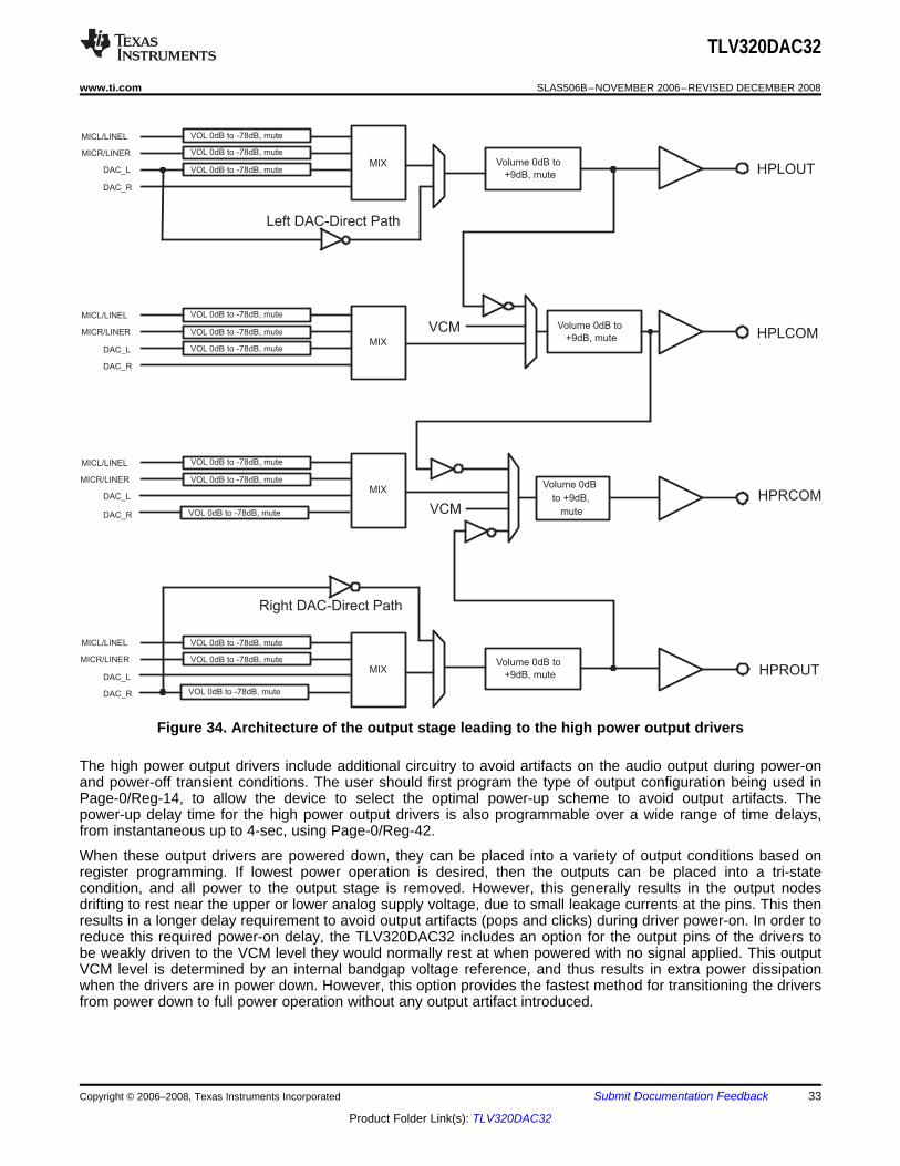
The output stage architecture with the volume control and mixing blocks leading to the high power output driversis shown in Figure 34. Note that each of these drivers have a output level control which allows gain adjustmentsup to +9dB on the output signal. Note that this output level adjustment is not intended to be used as a standardvolume control, but instead is included for additional full-scale output signal level control.
The output drivers, HPROUT and HPLOUT, include a direct connection path (L/R DAC_Direct) between thestereo DAC outputs and the output drivers. This pathway allows bypassing of the analog volume controls and themixing networks. This functionality provides the highest quality DAC playback performance while reducing powerdissipation, but this mode can only be utilized if the DAC output does not need to be mixed with the externalanalog input signals.
32 Submit Documentation Feedback Copyright © 2006–2008, Texas Instruments Incorporated
Product Folder Link(s): TLV320DAC32
Volume 0dB to
+9dB, mute
VCM
Volume 0dB to
+9dB, mute
VCM
HPLOUT
HPROUT
MIX
VOL 0dB to -78dB, mute
VOL 0dB to -78dB, mute
VOL 0dB to -78dB, mute
MIX
VOL 0dB to -78dB, mute
VOL 0dB to -78dB, mute
VOL 0dB to -78dB, mute
MIX
VOL 0dB to -78dB, mute
VOL 0dB to -78dB, mute
VOL 0dB to -78dB, mute
MIX
VOL 0dB to -78dB, mute
VOL 0dB to -78dB, mute
VOL 0dB to -78dB, mute
DAC_L
DAC_R
MICL/LINEL
MICR/LINER
DAC_L
DAC_R
MICL/LINEL
MICR/LINER
DAC_L
DAC_R
MICL/LINEL
MICR/LINER
DAC_L
DAC_R
MICL/LINEL
MICR/LINER
Left DAC-Direct Path
Right DAC-Direct Path
Volume 0dB
to +9dB,
mute
HPRCOM
Volume 0dB to
+9dB, mute HPLCOM
TLV320DAC32
www.ti.com........................................................................................................................................ SLAS506B–NOVEMBER 2006–REVISED DECEMBER 2008
Figure 34. Architecture of the output stage leading to the high power output drivers
The high power output drivers include additional circuitry to avoid artifacts on the audio output during power-onand power-off transient conditions. The user should first program the type of output configuration being used inPage-0/Reg-14, to allow the device to select the optimal power-up scheme to avoid output artifacts. Thepower-up delay time for the high power output drivers is also programmable over a wide range of time delays,from instantaneous up to 4-sec, using Page-0/Reg-42.
When these output drivers are powered down, they can be placed into a variety of output conditions based onregister programming. If lowest power operation is desired, then the outputs can be placed into a tri-statecondition, and all power to the output stage is removed. However, this generally results in the output nodesdrifting to rest near the upper or lower analog supply voltage, due to small leakage currents at the pins. This thenresults in a longer delay requirement to avoid output artifacts (pops and clicks) during driver power-on. In order toreduce this required power-on delay, the TLV320DAC32 includes an option for the output pins of the drivers tobe weakly driven to the VCM level they would normally rest at when powered with no signal applied. This outputVCM level is determined by an internal bandgap voltage reference, and thus results in extra power dissipationwhen the drivers are in power down. However, this option provides the fastest method for transitioning the driversfrom power down to full power operation without any output artifact introduced.
Copyright © 2006–2008, Texas Instruments Incorporated Submit Documentation Feedback 33
Product Folder Link(s): TLV320DAC32
SHORT CIRCUIT OUTPUT PROTECTION
JACK / HEADSET DETECTION
TLV320DAC32
SLAS506B–NOVEMBER 2006–REVISED DECEMBER 2008........................................................................................................................................ www.ti.com
The device includes a further option that falls between the other two – while it requires less power drawn whilethe output drivers are in power down, it also takes a slightly longer delay to power-up without artifact than if thebandgap reference is kept powered up. In this alternate mode, the powered-down output driver pin is weaklydriven to a voltage of approximately half the DRVDD1/2 supply level using an internal voltage divider. Thisvoltage will not match the actual VCM of a fully powered driver, but due to the output voltage being close to itsfinal value, a much shorter power-up delay time setting can be used and still avoid any audible output artifacts.These output voltage options are controlled in Page-0/Reg-42.
The high power output drivers can also be programmed at power up with the output level control in a highlyattenuated state, and when UN-Muted, the output driver will automatically slowly increase the gain to reach thedesired output level setting that was programmed prior to the Un-Mute setting. This capability is disabled bydefault setting but can be enabled in Page-0/Reg-40.
The TLV320DAC32 includes programmable short-circuit protection for the high power output drivers, formaximum flexibility in a given application. By default, if these output drivers are shorted, they will automaticallylimit the maximum amount of current that can be sourced to or sunk from a load, thereby protecting the devicefrom an over-current condition. In this mode, the user can read Page-0/Reg-95 to determine whether the part isin short-circuit protection or not, and then decide whether to program the device to power down the outputdrivers. However, the device includes further capability to automatically power down an output driver whenever itdoes enter into short-circuit protection, without requiring intervention from the user. In this case, the output driverwill stay in a power down condition until the user specifically programs it to power down and then power back upagain, to clear the short-circuit flag.
The TLV320DAC32 includes extensive capability to monitor a headphone, microphone, or headset jack,determine if a plug has been inserted into the jack, and then determine what type of headset/headphone is wiredto the plug. Figure 35 shows one configuration of the device that enables detection and determination of headsettype when a pseudo-differential (capless) stereo headphone output configuration is used. The registers used forthis function are Page-0/Reg 14, 37, 38, and 13. The type of headset detected can be read back fromPage-0/Reg-13. Note that for best results, it is recommended to select a MICBIAS value as high as possible, andto program the output driver common-mode level at a 1.35V or 1.5V level.
34 Submit Documentation Feedback Copyright © 2006–2008, Texas Instruments Incorporated
Product Folder Link(s): TLV320DAC32
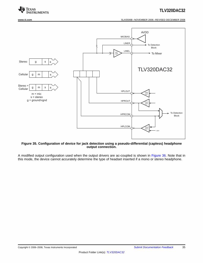
s
sg m
sg m s
sgStereo
Cellular
Stereo +Cellular
m = mics = stereo
g = ground/vgnd
LINER
LINEL
MICBIAS
MIC
AMP
AVDD
TLV320DAC32
To Detection
Block
To Mixer
HPLCOM PWR
AMP
1.35V
HPRCOMTo Detection
Block
HPLOUTPWR
AMP
HPROUTPWR
AMP
TLV320DAC32
www.ti.com........................................................................................................................................ SLAS506B–NOVEMBER 2006–REVISED DECEMBER 2008
Figure 35. Configuration of device for jack detection using a pseudo-differential (capless) headphoneoutput connection.
A modified output configuration used when the output drivers are ac-coupled is shown in Figure 36. Note that inthis mode, the device cannot accurately determine the type of headset inserted if a mono or stereo headphone.
Copyright © 2006–2008, Texas Instruments Incorporated Submit Documentation Feedback 35
Product Folder Link(s): TLV320DAC32
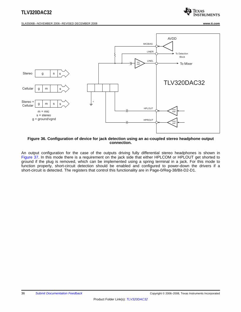
s
sg m
sg m s
sgStereo
Cellular
Stereo +Cellular
m = mics = stereo
g = ground/vgnd
LINER
LINEL
MICBIAS
MIC
AMP
AVDD
TLV320DAC32
To Detection
Block
To Mixer
HPLOUTPWR
AMP
HPROUTPWR
AMP
A
TLV320DAC32
SLAS506B–NOVEMBER 2006–REVISED DECEMBER 2008........................................................................................................................................ www.ti.com
Figure 36. Configuration of device for jack detection using an ac-coupled stereo headphone outputconnection.
An output configuration for the case of the outputs driving fully differential stereo headphones is shown inFigure 37. In this mode there is a requirement on the jack side that either HPLCOM or HPLOUT get shorted toground if the plug is removed, which can be implemented using a spring terminal in a jack. For this mode tofunction properly, short-circuit detection should be enabled and configured to power-down the drivers if ashort-circuit is detected. The registers that control this functionality are in Page-0/Reg-38/Bit-D2-D1.
36 Submit Documentation Feedback Copyright © 2006–2008, Texas Instruments Incorporated
Product Folder Link(s): TLV320DAC32
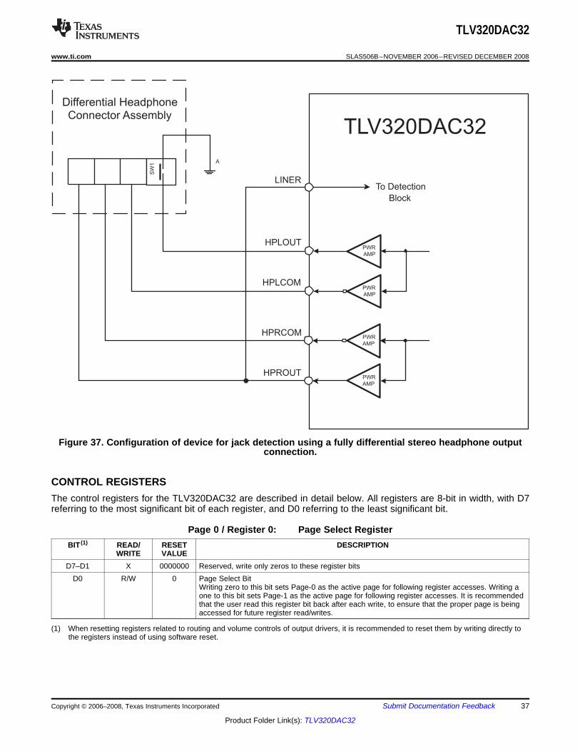
TLV320DAC32
A
HPLOUTPWR
AMP
HPLCOMPWR
AMP
HPRCOMPWR
AMP
HPROUTPWR
AMP
LINERTo Detection
Block
SW
1
Differential HeadphoneConnector Assembly
CONTROL REGISTERS
TLV320DAC32
www.ti.com........................................................................................................................................ SLAS506B–NOVEMBER 2006–REVISED DECEMBER 2008
Figure 37. Configuration of device for jack detection using a fully differential stereo headphone outputconnection.
The control registers for the TLV320DAC32 are described in detail below. All registers are 8-bit in width, with D7referring to the most significant bit of each register, and D0 referring to the least significant bit.
Page 0 / Register 0: Page Select RegisterBIT (1) READ/ RESET DESCRIPTION
WRITE VALUED7–D1 X 0000000 Reserved, write only zeros to these register bits
D0 R/W 0 Page Select BitWriting zero to this bit sets Page-0 as the active page for following register accesses. Writing aone to this bit sets Page-1 as the active page for following register accesses. It is recommendedthat the user read this register bit back after each write, to ensure that the proper page is beingaccessed for future register read/writes.
(1) When resetting registers related to routing and volume controls of output drivers, it is recommended to reset them by writing directly tothe registers instead of using software reset.
Copyright © 2006–2008, Texas Instruments Incorporated Submit Documentation Feedback 37
Product Folder Link(s): TLV320DAC32
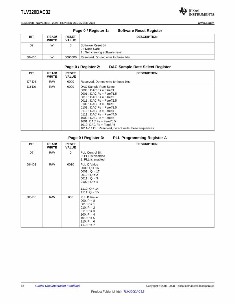
TLV320DAC32
SLAS506B–NOVEMBER 2006–REVISED DECEMBER 2008........................................................................................................................................ www.ti.com
Page 0 / Register 1: Software Reset RegisterBIT READ/ RESET DESCRIPTION
WRITE VALUED7 W 0 Software Reset Bit
0 : Don’t Care1 : Self clearing software reset
D6–D0 W 0000000 Reserved. Do not write to these bits.
Page 0 / Register 2: DAC Sample Rate Select RegisterBIT READ/ RESET DESCRIPTION
WRITE VALUED7-D4 R/W 0000 Reserved. Do not write to these bits.D3-D0 R/W 0000 DAC Sample Rate Select
0000 : DAC Fs = Fsref/10001 : DAC Fs = Fsref/1.50010 : DAC Fs = Fsref/20011 : DAC Fs = Fsref/2.50100 : DAC Fs = Fsref/30101 : DAC Fs = Fsref/3.50110 : DAC Fs = Fsref/40111 : DAC Fs = Fsref/4.51000 : DAC Fs = Fsref/51001: DAC Fs = Fsref/5.51010: DAC Fs = Fsref / 61011–1111 : Reserved, do not write these sequences.
Page 0 / Register 3: PLL Programming Register ABIT READ/ RESET DESCRIPTION
WRITE VALUED7 R/W 0 PLL Control Bit
0: PLL is disabled1: PLL is enabled
D6–D3 R/W 0010 PLL Q Value0000: Q = 160001 : Q = 170010 : Q = 20011 : Q = 30100 : Q = 4…1110: Q = 141111: Q = 15
D2–D0 R/W 000 PLL P Value000: P = 8001: P = 1010: P = 2011: P = 3100: P = 4101: P = 5110: P = 6111: P = 7
38 Submit Documentation Feedback Copyright © 2006–2008, Texas Instruments Incorporated
Product Folder Link(s): TLV320DAC32
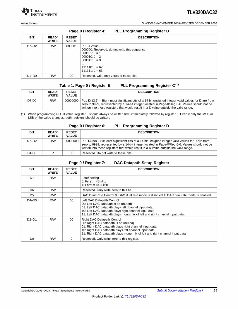
TLV320DAC32
www.ti.com........................................................................................................................................ SLAS506B–NOVEMBER 2006–REVISED DECEMBER 2008
Page 0 / Register 4: PLL Programming Register BBIT READ/ RESET DESCRIPTION
WRITE VALUED7–D2 R/W 000001 PLL J Value
000000: Reserved, do not write this sequence000001: J = 1000010: J = 2000011: J = 3…111110: J = 62111111: J = 63
D1–D0 R/W 00 Reserved, write only zeros to these bits
Table 1. Page 0 / Register 5: PLL Programming Register C (1)
BIT READ/ RESET DESCRIPTIONWRITE VALUE
D7-D0 R/W 00000000 PLL D(13:6) – Eight most significant bits of a 14-bit unsigned integer valid values for D are fromzero to 9999, represented by a 14-bit integer located in Page-0/Reg-5-6. Values should not bewritten into these registers that would result in a D value outside the valid range.
(1) When programming PLL D value, register 5 should always be written first, immediately followed by register 6. Even if only the MSB orLSB of the value changes, both registers should be written.
Page 0 / Register 6: PLL Programming Register DBIT READ/ RESET DESCRIPTION
WRITE VALUED7–D2 R/W 00000000 PLL D(5:0) – Six least significant bits of a 14-bit unsigned integer valid values for D are from
zero to 9999, represented by a 14-bit integer located in Page-0/Reg-5-6. Values should not bewritten into these registers that would result in a D value outside the valid range.
D1-D0 R 00 Reserved. Do not write to these bits.
Page 0 / Register 7: DAC Datapath Setup RegisterBIT READ/ RESET DESCRIPTION
WRITE VALUED7 R/W 0 Fsref setting
0: Fsref = 48-kHz1: Fsref = 44.1-kHz
D6 R/W 0 Reserved. Only write zero to this bit.D5 R/W 0 DAC Dual Rate Control 0: DAC dual rate mode is disabled 1: DAC dual rate mode is enabled
D4–D3 R/W 00 Left DAC Datapath Control00: Left DAC datapath is off (muted)01: Left DAC datapath plays left channel input data10: Left DAC datapath plays right channel input data11: Left DAC datapath plays mono mix of left and right channel input data
D2–D1 R/W 00 Right DAC Datapath Control00: Right DAC datapath is off (muted)01: Right DAC datapath plays right channel input data10: Right DAC datapath plays left channel input data11: Right DAC datapath plays mono mix of left and right channel input data
D0 R/W 0 Reserved. Only write zero to this register.
Copyright © 2006–2008, Texas Instruments Incorporated Submit Documentation Feedback 39
Product Folder Link(s): TLV320DAC32
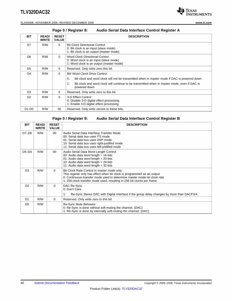
TLV320DAC32
SLAS506B–NOVEMBER 2006–REVISED DECEMBER 2008........................................................................................................................................ www.ti.com
Page 0 / Register 8: Audio Serial Data Interface Control Register ABIT READ/ RESET DESCRIPTION
WRITE VALUED7 R/W 0 Bit Clock Directional Control
0: Bit clock is an input (slave mode)1: Bit clock is an output (master mode)
D6 R/W 0 Word Clock Directional Control0: Word clock is an input (slave mode)1: Word clock is an output (master mode)
D5 R/W 0 Reserved. Only write zero this bit.D4 R/W 0 Bit/ Word Clock Drive Control
0: Bit clock and word clock will not be transmitted when in master mode if DAC is powered down1: Bit clock and word clock will continue to be transmitted when in master mode, even if DAC is
powered downD3 R/W 0 Reserved. Only write zero to this bit.D2 R/W 0 3-D Effect Control
0: Disable 3-D digital effect processing1: Enable 3-D digital effect processing
D1-D0 R/W 00 Reserved. Only write zeroes to these bits.
Page 0 / Register 9: Audio Serial Data Interface Control Register BBIT READ/ RESET DESCRIPTION
WRITE VALUED7–D6 R/W 00 Audio Serial Data Interface Transfer Mode
00: Serial data bus uses I2S mode01: Serial data bus uses DSP mode10: Serial data bus uses right-justified mode11: Serial data bus uses left-justified mode
D5–D4 R/W 00 Audio Serial Data Word Length Control00: Audio data word length = 16-bits01: Audio data word length = 20-bits10: Audio data word length = 24-bits11: Audio data word length = 32-bits
D3 R/W 0 Bit Clock Rate Control in master mode onlyThis register only has effect when bit clock is programmed as an output0: Continuous-transfer mode used to determine master mode bit clock rate1: 256-clock transfer mode used, resulting in 256 bit clocks per frame
D2 R/W 0 DAC Re-Sync0: Don’t Care1: Re-Sync Stereo DAC with Digital Interface if the group delay changes by more than DACFS/4.
D1 R/W 0 Reserved. Only write zero to this bit.D0 R/W Re-Sync Mute Behavior
0: Re-Sync is done without soft-muting the channel. (DAC)1: Re-Sync is done by internally soft-muting the channel. (DAC)
40 Submit Documentation Feedback Copyright © 2006–2008, Texas Instruments Incorporated
Product Folder Link(s): TLV320DAC32
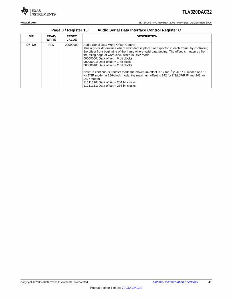
TLV320DAC32
www.ti.com........................................................................................................................................ SLAS506B–NOVEMBER 2006–REVISED DECEMBER 2008
Page 0 / Register 10: Audio Serial Data Interface Control Register CBIT READ/ RESET DESCRIPTION
WRITE VALUED7–D0 R/W 00000000 Audio Serial Data Word Offset Control
This register determines where valid data is placed or expected in each frame, by controllingthe offset from beginning of the frame where valid data begins. The offset is measured fromthe rising edge of word clock when in DSP mode.00000000: Data offset = 0 bit clocks00000001: Data offset = 1 bit clock00000010: Data offset = 2 bit clocks…Note: In continuous transfer mode the maximum offset is 17 for I2S/LJF/RJF modes and 16for DSP mode. In 256-clock mode, the maximum offset is 242 for I2S/LJF/RJF and 241 forDSP modes.11111110: Data offset = 254 bit clocks11111111: Data offset = 255 bit clocks
Copyright © 2006–2008, Texas Instruments Incorporated Submit Documentation Feedback 41
Product Folder Link(s): TLV320DAC32
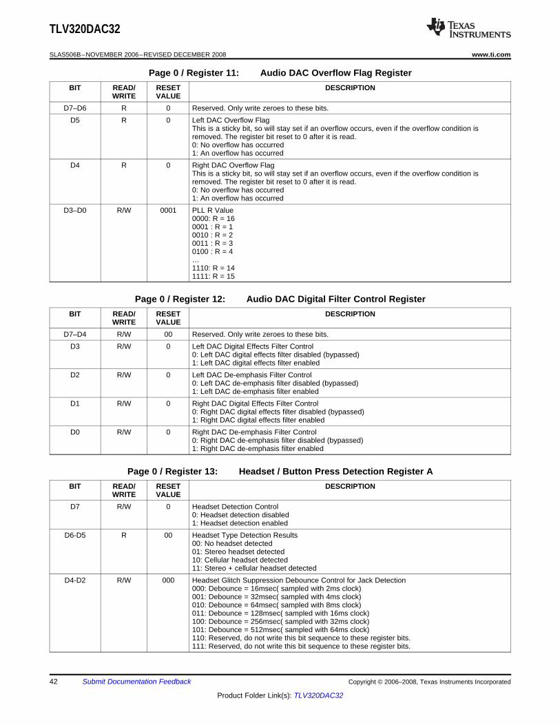
TLV320DAC32
SLAS506B–NOVEMBER 2006–REVISED DECEMBER 2008........................................................................................................................................ www.ti.com
Page 0 / Register 11: Audio DAC Overflow Flag RegisterBIT READ/ RESET DESCRIPTION
WRITE VALUED7–D6 R 0 Reserved. Only write zeroes to these bits.
D5 R 0 Left DAC Overflow FlagThis is a sticky bit, so will stay set if an overflow occurs, even if the overflow condition isremoved. The register bit reset to 0 after it is read.0: No overflow has occurred1: An overflow has occurred
D4 R 0 Right DAC Overflow FlagThis is a sticky bit, so will stay set if an overflow occurs, even if the overflow condition isremoved. The register bit reset to 0 after it is read.0: No overflow has occurred1: An overflow has occurred
D3–D0 R/W 0001 PLL R Value0000: R = 160001 : R = 10010 : R = 20011 : R = 30100 : R = 4…1110: R = 141111: R = 15
Page 0 / Register 12: Audio DAC Digital Filter Control RegisterBIT READ/ RESET DESCRIPTION
WRITE VALUED7–D4 R/W 00 Reserved. Only write zeroes to these bits.
D3 R/W 0 Left DAC Digital Effects Filter Control0: Left DAC digital effects filter disabled (bypassed)1: Left DAC digital effects filter enabled
D2 R/W 0 Left DAC De-emphasis Filter Control0: Left DAC de-emphasis filter disabled (bypassed)1: Left DAC de-emphasis filter enabled
D1 R/W 0 Right DAC Digital Effects Filter Control0: Right DAC digital effects filter disabled (bypassed)1: Right DAC digital effects filter enabled
D0 R/W 0 Right DAC De-emphasis Filter Control0: Right DAC de-emphasis filter disabled (bypassed)1: Right DAC de-emphasis filter enabled
Page 0 / Register 13: Headset / Button Press Detection Register ABIT READ/ RESET DESCRIPTION
WRITE VALUED7 R/W 0 Headset Detection Control
0: Headset detection disabled1: Headset detection enabled
D6-D5 R 00 Headset Type Detection Results00: No headset detected01: Stereo headset detected10: Cellular headset detected11: Stereo + cellular headset detected
D4-D2 R/W 000 Headset Glitch Suppression Debounce Control for Jack Detection000: Debounce = 16msec( sampled with 2ms clock)001: Debounce = 32msec( sampled with 4ms clock)010: Debounce = 64msec( sampled with 8ms clock)011: Debounce = 128msec( sampled with 16ms clock)100: Debounce = 256msec( sampled with 32ms clock)101: Debounce = 512msec( sampled with 64ms clock)110: Reserved, do not write this bit sequence to these register bits.111: Reserved, do not write this bit sequence to these register bits.
42 Submit Documentation Feedback Copyright © 2006–2008, Texas Instruments Incorporated
Product Folder Link(s): TLV320DAC32
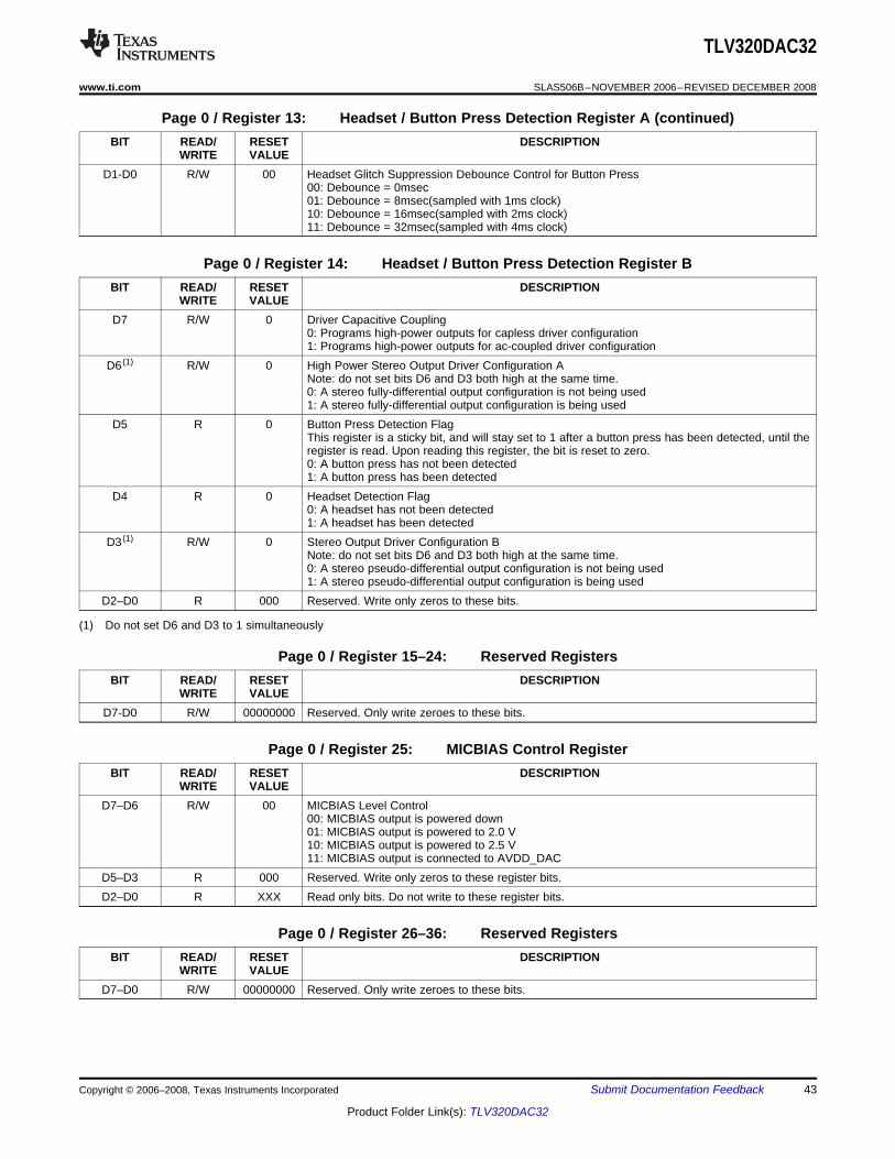
TLV320DAC32
www.ti.com........................................................................................................................................ SLAS506B–NOVEMBER 2006–REVISED DECEMBER 2008
Page 0 / Register 13: Headset / Button Press Detection Register A (continued)BIT READ/ RESET DESCRIPTION
WRITE VALUED1-D0 R/W 00 Headset Glitch Suppression Debounce Control for Button Press
00: Debounce = 0msec01: Debounce = 8msec(sampled with 1ms clock)10: Debounce = 16msec(sampled with 2ms clock)11: Debounce = 32msec(sampled with 4ms clock)
Page 0 / Register 14: Headset / Button Press Detection Register BBIT READ/ RESET DESCRIPTION
WRITE VALUED7 R/W 0 Driver Capacitive Coupling
0: Programs high-power outputs for capless driver configuration1: Programs high-power outputs for ac-coupled driver configuration
D6 (1) R/W 0 High Power Stereo Output Driver Configuration ANote: do not set bits D6 and D3 both high at the same time.0: A stereo fully-differential output configuration is not being used1: A stereo fully-differential output configuration is being used
D5 R 0 Button Press Detection FlagThis register is a sticky bit, and will stay set to 1 after a button press has been detected, until theregister is read. Upon reading this register, the bit is reset to zero.0: A button press has not been detected1: A button press has been detected
D4 R 0 Headset Detection Flag0: A headset has not been detected1: A headset has been detected
D3 (1) R/W 0 Stereo Output Driver Configuration BNote: do not set bits D6 and D3 both high at the same time.0: A stereo pseudo-differential output configuration is not being used1: A stereo pseudo-differential output configuration is being used
D2–D0 R 000 Reserved. Write only zeros to these bits.
(1) Do not set D6 and D3 to 1 simultaneously
Page 0 / Register 15–24: Reserved RegistersBIT READ/ RESET DESCRIPTION
WRITE VALUED7-D0 R/W 00000000 Reserved. Only write zeroes to these bits.
Page 0 / Register 25: MICBIAS Control RegisterBIT READ/ RESET DESCRIPTION
WRITE VALUED7–D6 R/W 00 MICBIAS Level Control
00: MICBIAS output is powered down01: MICBIAS output is powered to 2.0 V10: MICBIAS output is powered to 2.5 V11: MICBIAS output is connected to AVDD_DAC
D5–D3 R 000 Reserved. Write only zeros to these register bits.D2–D0 R XXX Read only bits. Do not write to these register bits.
Page 0 / Register 26–36: Reserved RegistersBIT READ/ RESET DESCRIPTION
WRITE VALUED7–D0 R/W 00000000 Reserved. Only write zeroes to these bits.
Copyright © 2006–2008, Texas Instruments Incorporated Submit Documentation Feedback 43
Product Folder Link(s): TLV320DAC32
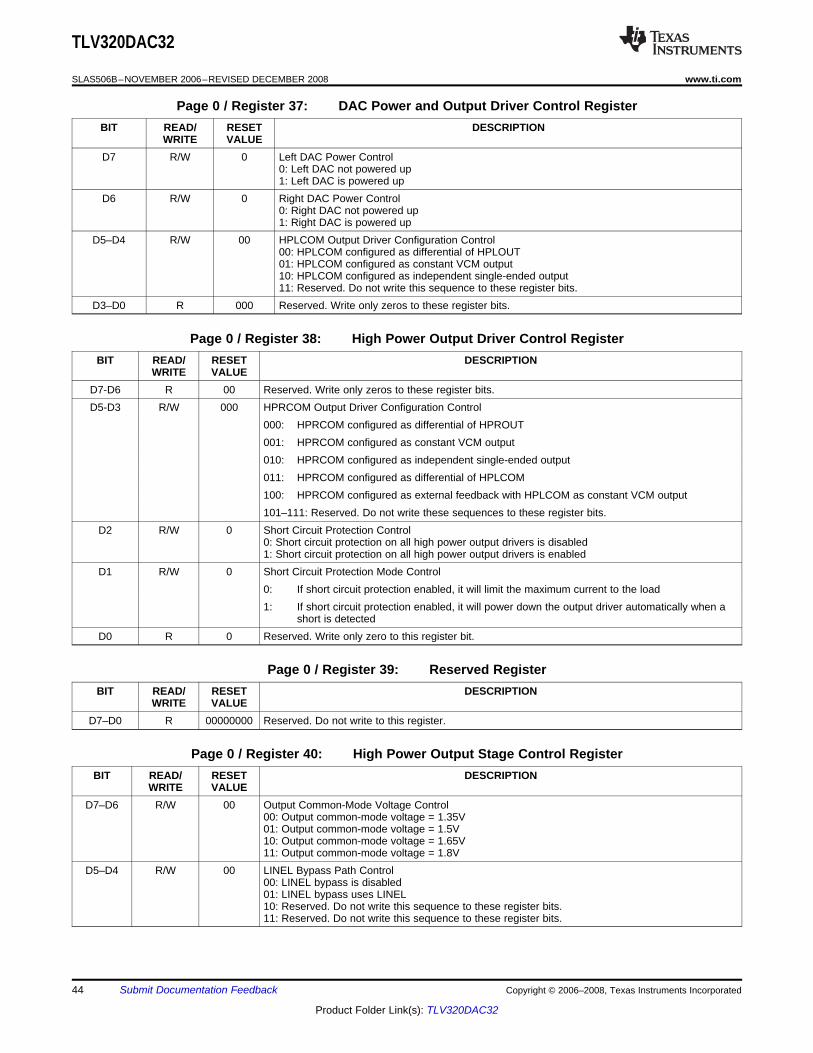
TLV320DAC32
SLAS506B–NOVEMBER 2006–REVISED DECEMBER 2008........................................................................................................................................ www.ti.com
Page 0 / Register 37: DAC Power and Output Driver Control RegisterBIT READ/ RESET DESCRIPTION
WRITE VALUED7 R/W 0 Left DAC Power Control
0: Left DAC not powered up1: Left DAC is powered up
D6 R/W 0 Right DAC Power Control0: Right DAC not powered up1: Right DAC is powered up
D5–D4 R/W 00 HPLCOM Output Driver Configuration Control00: HPLCOM configured as differential of HPLOUT01: HPLCOM configured as constant VCM output10: HPLCOM configured as independent single-ended output11: Reserved. Do not write this sequence to these register bits.
D3–D0 R 000 Reserved. Write only zeros to these register bits.
Page 0 / Register 38: High Power Output Driver Control RegisterBIT READ/ RESET DESCRIPTION
WRITE VALUED7-D6 R 00 Reserved. Write only zeros to these register bits.D5-D3 R/W 000 HPRCOM Output Driver Configuration Control
000: HPRCOM configured as differential of HPROUT001: HPRCOM configured as constant VCM output010: HPRCOM configured as independent single-ended output011: HPRCOM configured as differential of HPLCOM100: HPRCOM configured as external feedback with HPLCOM as constant VCM output101–111: Reserved. Do not write these sequences to these register bits.
D2 R/W 0 Short Circuit Protection Control0: Short circuit protection on all high power output drivers is disabled1: Short circuit protection on all high power output drivers is enabled
D1 R/W 0 Short Circuit Protection Mode Control0: If short circuit protection enabled, it will limit the maximum current to the load1: If short circuit protection enabled, it will power down the output driver automatically when a
short is detectedD0 R 0 Reserved. Write only zero to this register bit.
Page 0 / Register 39: Reserved RegisterBIT READ/ RESET DESCRIPTION
WRITE VALUED7–D0 R 00000000 Reserved. Do not write to this register.
Page 0 / Register 40: High Power Output Stage Control RegisterBIT READ/ RESET DESCRIPTION
WRITE VALUED7–D6 R/W 00 Output Common-Mode Voltage Control
00: Output common-mode voltage = 1.35V01: Output common-mode voltage = 1.5V10: Output common-mode voltage = 1.65V11: Output common-mode voltage = 1.8V
D5–D4 R/W 00 LINEL Bypass Path Control00: LINEL bypass is disabled01: LINEL bypass uses LINEL10: Reserved. Do not write this sequence to these register bits.11: Reserved. Do not write this sequence to these register bits.
44 Submit Documentation Feedback Copyright © 2006–2008, Texas Instruments Incorporated
Product Folder Link(s): TLV320DAC32
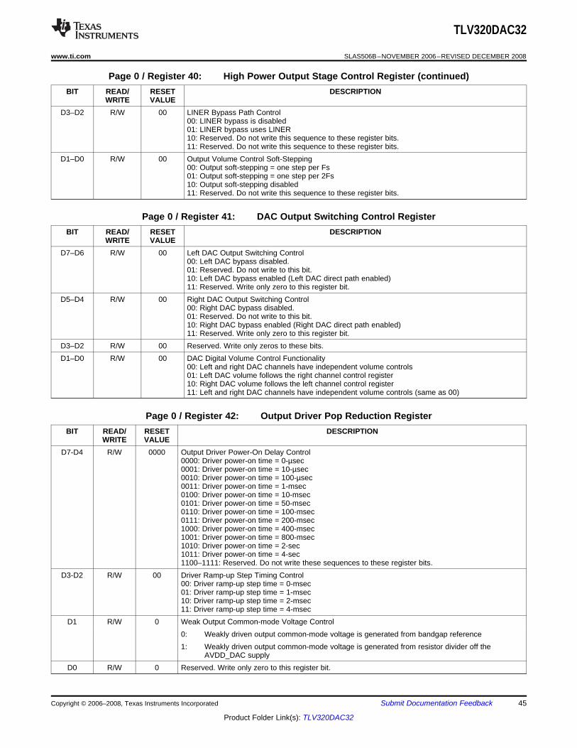
TLV320DAC32
www.ti.com........................................................................................................................................ SLAS506B–NOVEMBER 2006–REVISED DECEMBER 2008
Page 0 / Register 40: High Power Output Stage Control Register (continued)BIT READ/ RESET DESCRIPTION
WRITE VALUED3–D2 R/W 00 LINER Bypass Path Control
00: LINER bypass is disabled01: LINER bypass uses LINER10: Reserved. Do not write this sequence to these register bits.11: Reserved. Do not write this sequence to these register bits.
D1–D0 R/W 00 Output Volume Control Soft-Stepping00: Output soft-stepping = one step per Fs01: Output soft-stepping = one step per 2Fs10: Output soft-stepping disabled11: Reserved. Do not write this sequence to these register bits.
Page 0 / Register 41: DAC Output Switching Control RegisterBIT READ/ RESET DESCRIPTION
WRITE VALUED7–D6 R/W 00 Left DAC Output Switching Control
00: Left DAC bypass disabled.01: Reserved. Do not write to this bit.10: Left DAC bypass enabled (Left DAC direct path enabled)11: Reserved. Write only zero to this register bit.
D5–D4 R/W 00 Right DAC Output Switching Control00: Right DAC bypass disabled.01: Reserved. Do not write to this bit.10: Right DAC bypass enabled (Right DAC direct path enabled)11: Reserved. Write only zero to this register bit.
D3–D2 R/W 00 Reserved. Write only zeros to these bits.D1–D0 R/W 00 DAC Digital Volume Control Functionality
00: Left and right DAC channels have independent volume controls01: Left DAC volume follows the right channel control register10: Right DAC volume follows the left channel control register11: Left and right DAC channels have independent volume controls (same as 00)
Page 0 / Register 42: Output Driver Pop Reduction RegisterBIT READ/ RESET DESCRIPTION
WRITE VALUED7-D4 R/W 0000 Output Driver Power-On Delay Control
0000: Driver power-on time = 0-µsec0001: Driver power-on time = 10-µsec0010: Driver power-on time = 100-µsec0011: Driver power-on time = 1-msec0100: Driver power-on time = 10-msec0101: Driver power-on time = 50-msec0110: Driver power-on time = 100-msec0111: Driver power-on time = 200-msec1000: Driver power-on time = 400-msec1001: Driver power-on time = 800-msec1010: Driver power-on time = 2-sec1011: Driver power-on time = 4-sec1100–1111: Reserved. Do not write these sequences to these register bits.
D3-D2 R/W 00 Driver Ramp-up Step Timing Control00: Driver ramp-up step time = 0-msec01: Driver ramp-up step time = 1-msec10: Driver ramp-up step time = 2-msec11: Driver ramp-up step time = 4-msec
D1 R/W 0 Weak Output Common-mode Voltage Control0: Weakly driven output common-mode voltage is generated from bandgap reference1: Weakly driven output common-mode voltage is generated from resistor divider off the
AVDD_DAC supplyD0 R/W 0 Reserved. Write only zero to this register bit.
Copyright © 2006–2008, Texas Instruments Incorporated Submit Documentation Feedback 45
Product Folder Link(s): TLV320DAC32
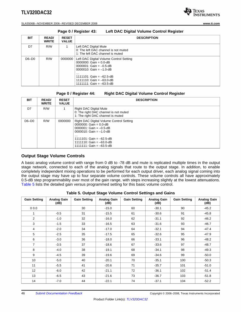
Output Stage Volume Controls
TLV320DAC32
SLAS506B–NOVEMBER 2006–REVISED DECEMBER 2008........................................................................................................................................ www.ti.com
Page 0 / Register 43: Left DAC Digital Volume Control RegisterBIT READ/ RESET DESCRIPTION
WRITE VALUED7 R/W 1 Left DAC Digital Mute
0: The left DAC channel is not muted1: The left DAC channel is muted
D6–D0 R/W 0000000 Left DAC Digital Volume Control Setting0000000: Gain = 0.0-dB0000001: Gain = –0.5-dB0000010: Gain = –1.0-dB…1111101: Gain = –62.5-dB1111110: Gain = –63.0-dB1111111: Gain = –63.5-dB
Page 0 / Register 44: Right DAC Digital Volume Control RegisterBIT READ/ RESET DESCRIPTION
WRITE VALUED7 R/W 1 Right DAC Digital Mute
0: The right DAC channel is not muted1: The right DAC channel is muted
D6–D0 R/W 0000000 Right DAC Digital Volume Control Setting0000000: Gain = 0.0-dB0000001: Gain = –0.5-dB0000010: Gain = –1.0-dB…1111101: Gain = –62.5-dB1111110: Gain = –63.0-dB1111111: Gain = –63.5-dB
A basic analog volume control with range from 0 dB to -78 dB and mute is replicated multiple times in the outputstage network, connected to each of the analog signals that route to the output stage. In addition, to enablecompletely independent mixing operations to be performed for each output driver, each analog signal coming intothe output stage may have up to four separate volume controls. These volume controls all have approximately0.5-dB step programmability over most of the gain range, with steps increasing slightly at the lowest attenuations.Table 5 lists the detailed gain versus programmed setting for this basic volume control.
Table 5. Output Stage Volume Control Settings and GainsGain Setting Analog Gain Gain Setting Analog Gain Gain Setting Analog Gain Gain Setting Analog Gain
(dB) (dB) (dB) (dB)0 0.0 30 -15.0 60 -30.1 90 -45.2
1 -0.5 31 -15.5 61 -30.6 91 -45.82 -1.0 32 -16.0 62 -31.1 92 -46.23 -1.5 33 -16.5 63 -31.6 93 -46.74 -2.0 34 -17.0 64 -32.1 94 -47.45 -2.5 35 -17.5 65 -32.6 95 -47.96 -3.0 36 -18.0 66 -33.1 96 -48.27 -3.5 37 -18.6 67 -33.6 97 -48.78 -4.0 38 -19.1 68 -34.1 98 -49.39 -4.5 39 -19.6 69 -34.6 99 -50.010 -5.0 40 -20.1 70 -35.1 100 -50.311 -5.5 41 -20.6 71 -35.7 101 -51.012 -6.0 42 -21.1 72 -36.1 102 -51.413 -6.5 43 -21.6 73 -36.7 103 -51.814 -7.0 44 -22.1 74 -37.1 104 -52.2
46 Submit Documentation Feedback Copyright © 2006–2008, Texas Instruments Incorporated
Product Folder Link(s): TLV320DAC32
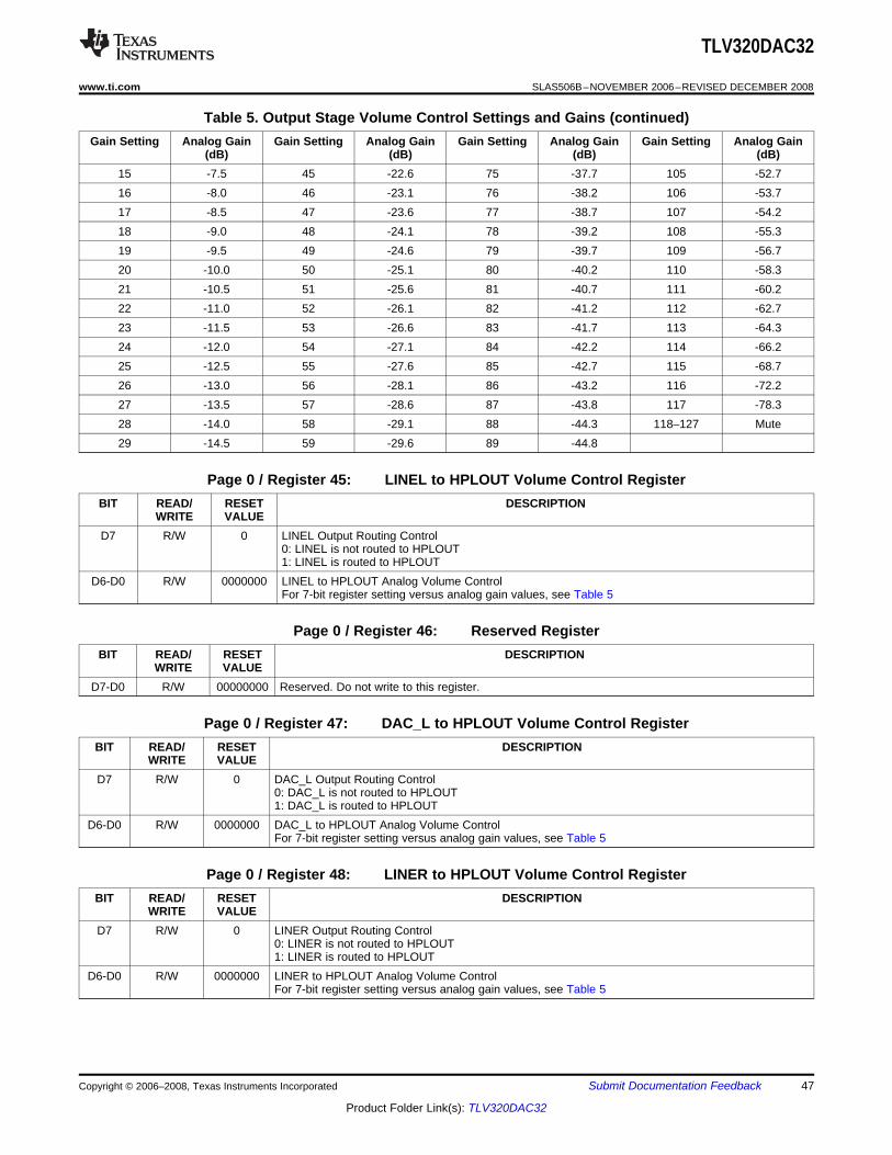
TLV320DAC32
www.ti.com........................................................................................................................................ SLAS506B–NOVEMBER 2006–REVISED DECEMBER 2008
Table 5. Output Stage Volume Control Settings and Gains (continued)Gain Setting Analog Gain Gain Setting Analog Gain Gain Setting Analog Gain Gain Setting Analog Gain
(dB) (dB) (dB) (dB)15 -7.5 45 -22.6 75 -37.7 105 -52.716 -8.0 46 -23.1 76 -38.2 106 -53.717 -8.5 47 -23.6 77 -38.7 107 -54.218 -9.0 48 -24.1 78 -39.2 108 -55.319 -9.5 49 -24.6 79 -39.7 109 -56.720 -10.0 50 -25.1 80 -40.2 110 -58.321 -10.5 51 -25.6 81 -40.7 111 -60.222 -11.0 52 -26.1 82 -41.2 112 -62.723 -11.5 53 -26.6 83 -41.7 113 -64.324 -12.0 54 -27.1 84 -42.2 114 -66.225 -12.5 55 -27.6 85 -42.7 115 -68.726 -13.0 56 -28.1 86 -43.2 116 -72.227 -13.5 57 -28.6 87 -43.8 117 -78.328 -14.0 58 -29.1 88 -44.3 118–127 Mute29 -14.5 59 -29.6 89 -44.8
Page 0 / Register 45: LINEL to HPLOUT Volume Control RegisterBIT READ/ RESET DESCRIPTION
WRITE VALUED7 R/W 0 LINEL Output Routing Control
0: LINEL is not routed to HPLOUT1: LINEL is routed to HPLOUT
D6-D0 R/W 0000000 LINEL to HPLOUT Analog Volume ControlFor 7-bit register setting versus analog gain values, see Table 5
Page 0 / Register 46: Reserved RegisterBIT READ/ RESET DESCRIPTION
WRITE VALUED7-D0 R/W 00000000 Reserved. Do not write to this register.
Page 0 / Register 47: DAC_L to HPLOUT Volume Control RegisterBIT READ/ RESET DESCRIPTION
WRITE VALUED7 R/W 0 DAC_L Output Routing Control
0: DAC_L is not routed to HPLOUT1: DAC_L is routed to HPLOUT
D6-D0 R/W 0000000 DAC_L to HPLOUT Analog Volume ControlFor 7-bit register setting versus analog gain values, see Table 5
Page 0 / Register 48: LINER to HPLOUT Volume Control RegisterBIT READ/ RESET DESCRIPTION
WRITE VALUED7 R/W 0 LINER Output Routing Control
0: LINER is not routed to HPLOUT1: LINER is routed to HPLOUT
D6-D0 R/W 0000000 LINER to HPLOUT Analog Volume ControlFor 7-bit register setting versus analog gain values, see Table 5
Copyright © 2006–2008, Texas Instruments Incorporated Submit Documentation Feedback 47
Product Folder Link(s): TLV320DAC32
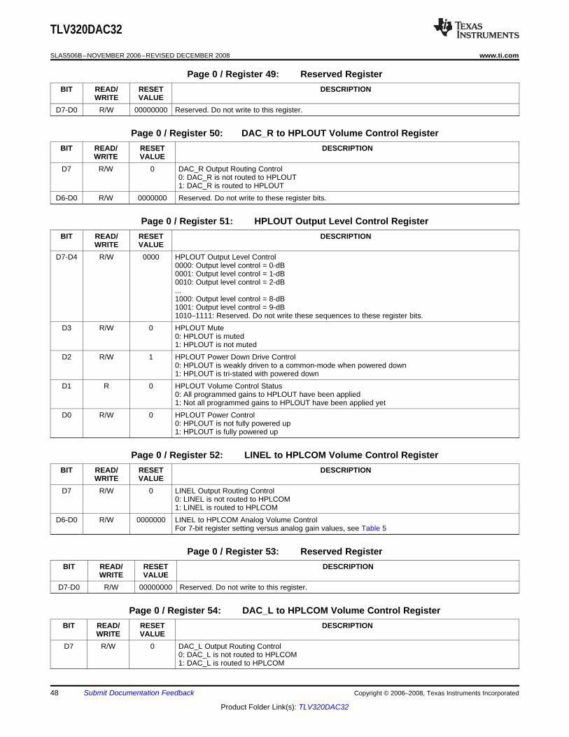
TLV320DAC32
SLAS506B–NOVEMBER 2006–REVISED DECEMBER 2008........................................................................................................................................ www.ti.com
Page 0 / Register 49: Reserved RegisterBIT READ/ RESET DESCRIPTION
WRITE VALUED7-D0 R/W 00000000 Reserved. Do not write to this register.
Page 0 / Register 50: DAC_R to HPLOUT Volume Control RegisterBIT READ/ RESET DESCRIPTION
WRITE VALUED7 R/W 0 DAC_R Output Routing Control
0: DAC_R is not routed to HPLOUT1: DAC_R is routed to HPLOUT
D6-D0 R/W 0000000 Reserved. Do not write to these register bits.
Page 0 / Register 51: HPLOUT Output Level Control RegisterBIT READ/ RESET DESCRIPTION
WRITE VALUED7-D4 R/W 0000 HPLOUT Output Level Control
0000: Output level control = 0-dB0001: Output level control = 1-dB0010: Output level control = 2-dB...1000: Output level control = 8-dB1001: Output level control = 9-dB1010–1111: Reserved. Do not write these sequences to these register bits.
D3 R/W 0 HPLOUT Mute0: HPLOUT is muted1: HPLOUT is not muted
D2 R/W 1 HPLOUT Power Down Drive Control0: HPLOUT is weakly driven to a common-mode when powered down1: HPLOUT is tri-stated with powered down
D1 R 0 HPLOUT Volume Control Status0: All programmed gains to HPLOUT have been applied1: Not all programmed gains to HPLOUT have been applied yet
D0 R/W 0 HPLOUT Power Control0: HPLOUT is not fully powered up1: HPLOUT is fully powered up
Page 0 / Register 52: LINEL to HPLCOM Volume Control RegisterBIT READ/ RESET DESCRIPTION
WRITE VALUED7 R/W 0 LINEL Output Routing Control
0: LINEL is not routed to HPLCOM1: LINEL is routed to HPLCOM
D6-D0 R/W 0000000 LINEL to HPLCOM Analog Volume ControlFor 7-bit register setting versus analog gain values, see Table 5
Page 0 / Register 53: Reserved RegisterBIT READ/ RESET DESCRIPTION
WRITE VALUED7-D0 R/W 00000000 Reserved. Do not write to this register.
Page 0 / Register 54: DAC_L to HPLCOM Volume Control RegisterBIT READ/ RESET DESCRIPTION
WRITE VALUED7 R/W 0 DAC_L Output Routing Control
0: DAC_L is not routed to HPLCOM1: DAC_L is routed to HPLCOM
48 Submit Documentation Feedback Copyright © 2006–2008, Texas Instruments Incorporated
Product Folder Link(s): TLV320DAC32
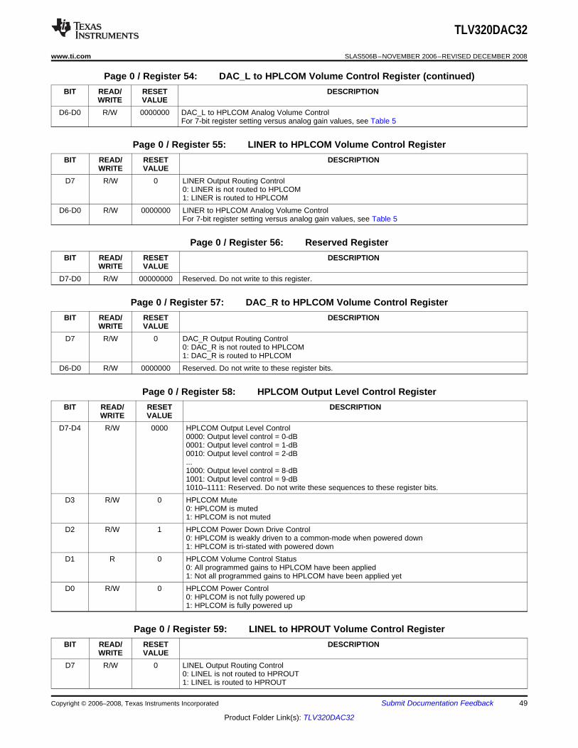
TLV320DAC32
www.ti.com........................................................................................................................................ SLAS506B–NOVEMBER 2006–REVISED DECEMBER 2008
Page 0 / Register 54: DAC_L to HPLCOM Volume Control Register (continued)BIT READ/ RESET DESCRIPTION
WRITE VALUED6-D0 R/W 0000000 DAC_L to HPLCOM Analog Volume Control
For 7-bit register setting versus analog gain values, see Table 5
Page 0 / Register 55: LINER to HPLCOM Volume Control RegisterBIT READ/ RESET DESCRIPTION
WRITE VALUED7 R/W 0 LINER Output Routing Control
0: LINER is not routed to HPLCOM1: LINER is routed to HPLCOM
D6-D0 R/W 0000000 LINER to HPLCOM Analog Volume ControlFor 7-bit register setting versus analog gain values, see Table 5
Page 0 / Register 56: Reserved RegisterBIT READ/ RESET DESCRIPTION
WRITE VALUED7-D0 R/W 00000000 Reserved. Do not write to this register.
Page 0 / Register 57: DAC_R to HPLCOM Volume Control RegisterBIT READ/ RESET DESCRIPTION
WRITE VALUED7 R/W 0 DAC_R Output Routing Control
0: DAC_R is not routed to HPLCOM1: DAC_R is routed to HPLCOM
D6-D0 R/W 0000000 Reserved. Do not write to these register bits.
Page 0 / Register 58: HPLCOM Output Level Control RegisterBIT READ/ RESET DESCRIPTION
WRITE VALUED7-D4 R/W 0000 HPLCOM Output Level Control
0000: Output level control = 0-dB0001: Output level control = 1-dB0010: Output level control = 2-dB...1000: Output level control = 8-dB1001: Output level control = 9-dB1010–1111: Reserved. Do not write these sequences to these register bits.
D3 R/W 0 HPLCOM Mute0: HPLCOM is muted1: HPLCOM is not muted
D2 R/W 1 HPLCOM Power Down Drive Control0: HPLCOM is weakly driven to a common-mode when powered down1: HPLCOM is tri-stated with powered down
D1 R 0 HPLCOM Volume Control Status0: All programmed gains to HPLCOM have been applied1: Not all programmed gains to HPLCOM have been applied yet
D0 R/W 0 HPLCOM Power Control0: HPLCOM is not fully powered up1: HPLCOM is fully powered up
Page 0 / Register 59: LINEL to HPROUT Volume Control RegisterBIT READ/ RESET DESCRIPTION
WRITE VALUED7 R/W 0 LINEL Output Routing Control
0: LINEL is not routed to HPROUT1: LINEL is routed to HPROUT
Copyright © 2006–2008, Texas Instruments Incorporated Submit Documentation Feedback 49
Product Folder Link(s): TLV320DAC32
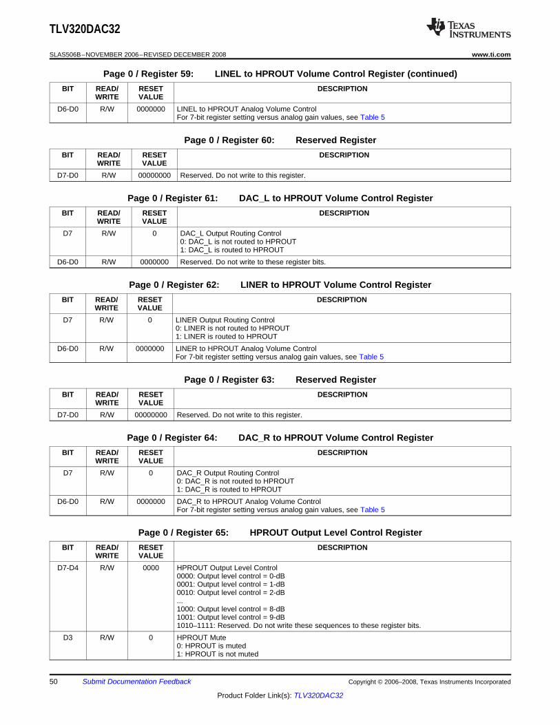
TLV320DAC32
SLAS506B–NOVEMBER 2006–REVISED DECEMBER 2008........................................................................................................................................ www.ti.com
Page 0 / Register 59: LINEL to HPROUT Volume Control Register (continued)BIT READ/ RESET DESCRIPTION
WRITE VALUED6-D0 R/W 0000000 LINEL to HPROUT Analog Volume Control
For 7-bit register setting versus analog gain values, see Table 5
Page 0 / Register 60: Reserved RegisterBIT READ/ RESET DESCRIPTION
WRITE VALUED7-D0 R/W 00000000 Reserved. Do not write to this register.
Page 0 / Register 61: DAC_L to HPROUT Volume Control RegisterBIT READ/ RESET DESCRIPTION
WRITE VALUED7 R/W 0 DAC_L Output Routing Control
0: DAC_L is not routed to HPROUT1: DAC_L is routed to HPROUT
D6-D0 R/W 0000000 Reserved. Do not write to these register bits.
Page 0 / Register 62: LINER to HPROUT Volume Control RegisterBIT READ/ RESET DESCRIPTION
WRITE VALUED7 R/W 0 LINER Output Routing Control
0: LINER is not routed to HPROUT1: LINER is routed to HPROUT
D6-D0 R/W 0000000 LINER to HPROUT Analog Volume ControlFor 7-bit register setting versus analog gain values, see Table 5
Page 0 / Register 63: Reserved RegisterBIT READ/ RESET DESCRIPTION
WRITE VALUED7-D0 R/W 00000000 Reserved. Do not write to this register.
Page 0 / Register 64: DAC_R to HPROUT Volume Control RegisterBIT READ/ RESET DESCRIPTION
WRITE VALUED7 R/W 0 DAC_R Output Routing Control
0: DAC_R is not routed to HPROUT1: DAC_R is routed to HPROUT
D6-D0 R/W 0000000 DAC_R to HPROUT Analog Volume ControlFor 7-bit register setting versus analog gain values, see Table 5
Page 0 / Register 65: HPROUT Output Level Control RegisterBIT READ/ RESET DESCRIPTION
WRITE VALUED7-D4 R/W 0000 HPROUT Output Level Control
0000: Output level control = 0-dB0001: Output level control = 1-dB0010: Output level control = 2-dB...1000: Output level control = 8-dB1001: Output level control = 9-dB1010–1111: Reserved. Do not write these sequences to these register bits.
D3 R/W 0 HPROUT Mute0: HPROUT is muted1: HPROUT is not muted
50 Submit Documentation Feedback Copyright © 2006–2008, Texas Instruments Incorporated
Product Folder Link(s): TLV320DAC32
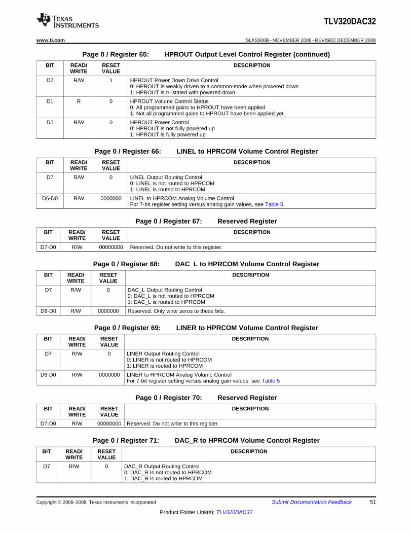
TLV320DAC32
www.ti.com........................................................................................................................................ SLAS506B–NOVEMBER 2006–REVISED DECEMBER 2008
Page 0 / Register 65: HPROUT Output Level Control Register (continued)BIT READ/ RESET DESCRIPTION
WRITE VALUED2 R/W 1 HPROUT Power Down Drive Control
0: HPROUT is weakly driven to a common-mode when powered down1: HPROUT is tri-stated with powered down
D1 R 0 HPROUT Volume Control Status0: All programmed gains to HPROUT have been applied1: Not all programmed gains to HPROUT have been applied yet
D0 R/W 0 HPROUT Power Control0: HPROUT is not fully powered up1: HPROUT is fully powered up
Page 0 / Register 66: LINEL to HPRCOM Volume Control RegisterBIT READ/ RESET DESCRIPTION
WRITE VALUED7 R/W 0 LINEL Output Routing Control
0: LINEL is not routed to HPRCOM1: LINEL is routed to HPRCOM
D6-D0 R/W 0000000 LINEL to HPRCOM Analog Volume ControlFor 7-bit register setting versus analog gain values, see Table 5
Page 0 / Register 67: Reserved RegisterBIT READ/ RESET DESCRIPTION
WRITE VALUED7-D0 R/W 00000000 Reserved. Do not write to this register.
Page 0 / Register 68: DAC_L to HPRCOM Volume Control RegisterBIT READ/ RESET DESCRIPTION
WRITE VALUED7 R/W 0 DAC_L Output Routing Control
0: DAC_L is not routed to HPRCOM1: DAC_L is routed to HPRCOM
D6-D0 R/W 0000000 Reserved. Only write zeros to these bits.
Page 0 / Register 69: LINER to HPRCOM Volume Control RegisterBIT READ/ RESET DESCRIPTION
WRITE VALUED7 R/W 0 LINER Output Routing Control
0: LINER is not routed to HPRCOM1: LINER is routed to HPRCOM
D6-D0 R/W 0000000 LINER to HPRCOM Analog Volume ControlFor 7-bit register setting versus analog gain values, see Table 5
Page 0 / Register 70: Reserved RegisterBIT READ/ RESET DESCRIPTION
WRITE VALUED7-D0 R/W 00000000 Reserved. Do not write to this register.
Page 0 / Register 71: DAC_R to HPRCOM Volume Control RegisterBIT READ/ RESET DESCRIPTION
WRITE VALUED7 R/W 0 DAC_R Output Routing Control
0: DAC_R is not routed to HPRCOM1: DAC_R is routed to HPRCOM
Copyright © 2006–2008, Texas Instruments Incorporated Submit Documentation Feedback 51
Product Folder Link(s): TLV320DAC32
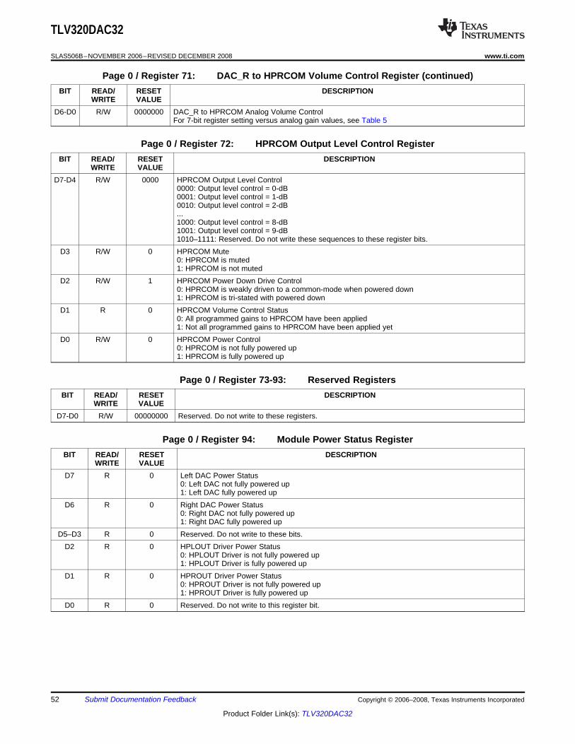
TLV320DAC32
SLAS506B–NOVEMBER 2006–REVISED DECEMBER 2008........................................................................................................................................ www.ti.com
Page 0 / Register 71: DAC_R to HPRCOM Volume Control Register (continued)BIT READ/ RESET DESCRIPTION
WRITE VALUED6-D0 R/W 0000000 DAC_R to HPRCOM Analog Volume Control
For 7-bit register setting versus analog gain values, see Table 5
Page 0 / Register 72: HPRCOM Output Level Control RegisterBIT READ/ RESET DESCRIPTION
WRITE VALUED7-D4 R/W 0000 HPRCOM Output Level Control
0000: Output level control = 0-dB0001: Output level control = 1-dB0010: Output level control = 2-dB...1000: Output level control = 8-dB1001: Output level control = 9-dB1010–1111: Reserved. Do not write these sequences to these register bits.
D3 R/W 0 HPRCOM Mute0: HPRCOM is muted1: HPRCOM is not muted
D2 R/W 1 HPRCOM Power Down Drive Control0: HPRCOM is weakly driven to a common-mode when powered down1: HPRCOM is tri-stated with powered down
D1 R 0 HPRCOM Volume Control Status0: All programmed gains to HPRCOM have been applied1: Not all programmed gains to HPRCOM have been applied yet
D0 R/W 0 HPRCOM Power Control0: HPRCOM is not fully powered up1: HPRCOM is fully powered up
Page 0 / Register 73-93: Reserved RegistersBIT READ/ RESET DESCRIPTION
WRITE VALUED7-D0 R/W 00000000 Reserved. Do not write to these registers.
Page 0 / Register 94: Module Power Status RegisterBIT READ/ RESET DESCRIPTION
WRITE VALUED7 R 0 Left DAC Power Status
0: Left DAC not fully powered up1: Left DAC fully powered up
D6 R 0 Right DAC Power Status0: Right DAC not fully powered up1: Right DAC fully powered up
D5–D3 R 0 Reserved. Do not write to these bits.D2 R 0 HPLOUT Driver Power Status
0: HPLOUT Driver is not fully powered up1: HPLOUT Driver is fully powered up
D1 R 0 HPROUT Driver Power Status0: HPROUT Driver is not fully powered up1: HPROUT Driver is fully powered up
D0 R 0 Reserved. Do not write to this register bit.
52 Submit Documentation Feedback Copyright © 2006–2008, Texas Instruments Incorporated
Product Folder Link(s): TLV320DAC32
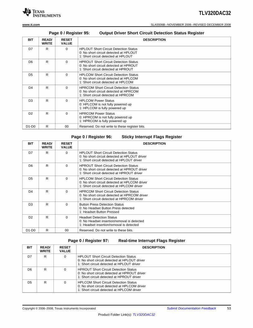
TLV320DAC32
www.ti.com........................................................................................................................................ SLAS506B–NOVEMBER 2006–REVISED DECEMBER 2008
Page 0 / Register 95: Output Driver Short Circuit Detection Status RegisterBIT READ/ RESET DESCRIPTION
WRITE VALUED7 R 0 HPLOUT Short Circuit Detection Status
0: No short circuit detected at HPLOUT1: Short circuit detected at HPLOUT
D6 R 0 HPROUT Short Circuit Detection Status0: No short circuit detected at HPROUT1: Short circuit detected at HPROUT
D5 R 0 HPLCOM Short Circuit Detection Status0: No short circuit detected at HPLCOM1: Short circuit detected at HPLCOM
D4 R 0 HPRCOM Short Circuit Detection Status0: No short circuit detected at HPRCOM1: Short circuit detected at HPRCOM
D3 R 0 HPLCOM Power Status0: HPLCOM is not fully powered up1: HPLCOM is fully powered up
D2 R 0 HPRCOM Power Status0: HPRCOM is not fully powered up1: HPRCOM is fully powered up
D1-D0 R 00 Reserved. Do not write to these register bits.
Page 0 / Register 96: Sticky Interrupt Flags RegisterBIT READ/ RESET DESCRIPTION
WRITE VALUED7 R 0 HPLOUT Short Circuit Detection Status
0: No short circuit detected at HPLOUT driver1: Short circuit detected at HPLOUT driver
D6 R 0 HPROUT Short Circuit Detection Status0: No short circuit detected at HPROUT driver1: Short circuit detected at HPROUT driver
D5 R 0 HPLCOM Short Circuit Detection Status0: No short circuit detected at HPLCOM driver1: Short circuit detected at HPLCOM driver
D4 R 0 HPRCOM Short Circuit Detection Status0: No short circuit detected at HPRCOM driver1: Short circuit detected at HPRCOM driver
D3 R 0 Button Press Detection Status0: No Headset Button Press detected1: Headset Button Pressed
D2 R 0 Headset Detection Status0: No Headset insertion/removal is detected1: Headset insertion/removal is detected
D1-D0 R 00 Reserved. Do not write to these bits.
Page 0 / Register 97: Real-time Interrupt Flags RegisterBIT READ/ RESET DESCRIPTION
WRITE VALUED7 R 0 HPLOUT Short Circuit Detection Status
0: No short circuit detected at HPLOUT driver1: Short circuit detected at HPLOUT driver
D6 R 0 HPROUT Short Circuit Detection Status0: No short circuit detected at HPROUT driver1: Short circuit detected at HPROUT driver
D5 R 0 HPLCOM Short Circuit Detection Status0: No short circuit detected at HPLCOM driver1: Short circuit detected at HPLCOM driver
Copyright © 2006–2008, Texas Instruments Incorporated Submit Documentation Feedback 53
Product Folder Link(s): TLV320DAC32
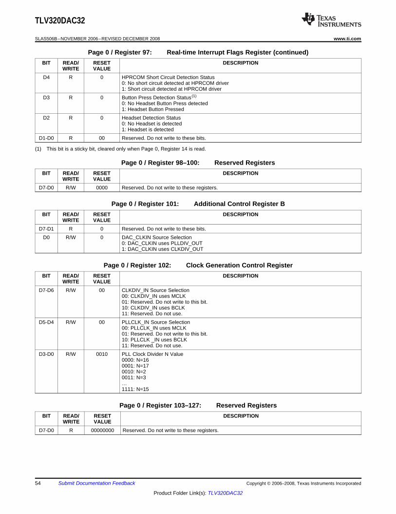
TLV320DAC32
SLAS506B–NOVEMBER 2006–REVISED DECEMBER 2008........................................................................................................................................ www.ti.com
Page 0 / Register 97: Real-time Interrupt Flags Register (continued)BIT READ/ RESET DESCRIPTION
WRITE VALUED4 R 0 HPRCOM Short Circuit Detection Status
0: No short circuit detected at HPRCOM driver1: Short circuit detected at HPRCOM driver
D3 R 0 Button Press Detection Status (1)
0: No Headset Button Press detected1: Headset Button Pressed
D2 R 0 Headset Detection Status0: No Headset is detected1: Headset is detected
D1-D0 R 00 Reserved. Do not write to these bits.
(1) This bit is a sticky bit, cleared only when Page 0, Register 14 is read.
Page 0 / Register 98–100: Reserved RegistersBIT READ/ RESET DESCRIPTION
WRITE VALUED7-D0 R/W 0000 Reserved. Do not write to these registers.
Page 0 / Register 101: Additional Control Register BBIT READ/ RESET DESCRIPTION
WRITE VALUED7-D1 R 0 Reserved. Do not write to these bits.
D0 R/W 0 DAC_CLKIN Source Selection0: DAC_CLKIN uses PLLDIV_OUT1: DAC_CLKIN uses CLKDIV_OUT
Page 0 / Register 102: Clock Generation Control RegisterBIT READ/ RESET DESCRIPTION
WRITE VALUED7-D6 R/W 00 CLKDIV_IN Source Selection
00: CLKDIV_IN uses MCLK01: Reserved. Do not write to this bit.10: CLKDIV_IN uses BCLK11: Reserved. Do not use.
D5-D4 R/W 00 PLLCLK_IN Source Selection00: PLLCLK_IN uses MCLK01: Reserved. Do not write to this bit.10: PLLCLK _IN uses BCLK11: Reserved. Do not use.
D3-D0 R/W 0010 PLL Clock Divider N Value0000: N=160001: N=170010: N=20011: N=3…1111: N=15
Page 0 / Register 103–127: Reserved RegistersBIT READ/ RESET DESCRIPTION
WRITE VALUED7-D0 R 00000000 Reserved. Do not write to these registers.
54 Submit Documentation Feedback Copyright © 2006–2008, Texas Instruments Incorporated
Product Folder Link(s): TLV320DAC32
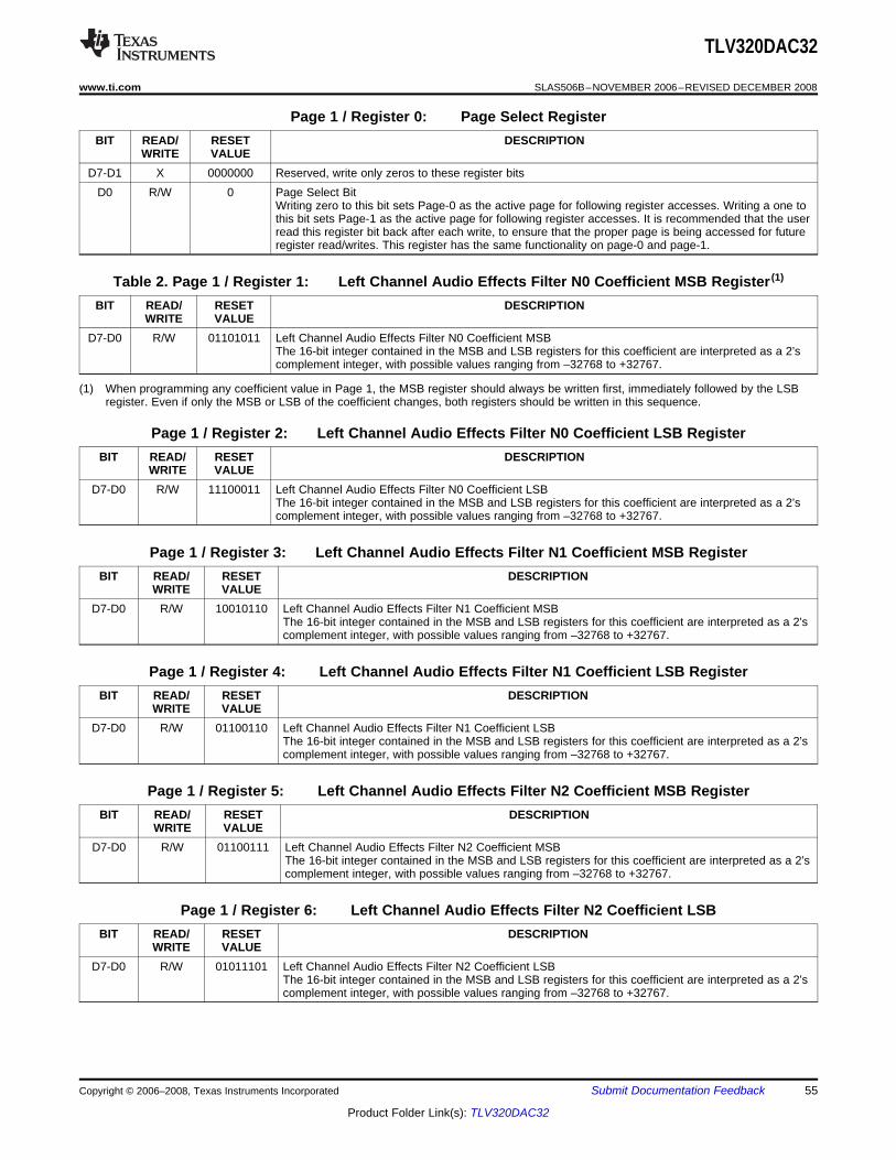
TLV320DAC32
www.ti.com........................................................................................................................................ SLAS506B–NOVEMBER 2006–REVISED DECEMBER 2008
Page 1 / Register 0: Page Select RegisterBIT READ/ RESET DESCRIPTION
WRITE VALUED7-D1 X 0000000 Reserved, write only zeros to these register bits
D0 R/W 0 Page Select BitWriting zero to this bit sets Page-0 as the active page for following register accesses. Writing a one tothis bit sets Page-1 as the active page for following register accesses. It is recommended that the userread this register bit back after each write, to ensure that the proper page is being accessed for futureregister read/writes. This register has the same functionality on page-0 and page-1.
Table 2. Page 1 / Register 1: Left Channel Audio Effects Filter N0 Coefficient MSB Register (1)
BIT READ/ RESET DESCRIPTIONWRITE VALUE
D7-D0 R/W 01101011 Left Channel Audio Effects Filter N0 Coefficient MSBThe 16-bit integer contained in the MSB and LSB registers for this coefficient are interpreted as a 2’scomplement integer, with possible values ranging from –32768 to +32767.
(1) When programming any coefficient value in Page 1, the MSB register should always be written first, immediately followed by the LSBregister. Even if only the MSB or LSB of the coefficient changes, both registers should be written in this sequence.
Page 1 / Register 2: Left Channel Audio Effects Filter N0 Coefficient LSB RegisterBIT READ/ RESET DESCRIPTION
WRITE VALUED7-D0 R/W 11100011 Left Channel Audio Effects Filter N0 Coefficient LSB
The 16-bit integer contained in the MSB and LSB registers for this coefficient are interpreted as a 2’scomplement integer, with possible values ranging from –32768 to +32767.
Page 1 / Register 3: Left Channel Audio Effects Filter N1 Coefficient MSB RegisterBIT READ/ RESET DESCRIPTION
WRITE VALUED7-D0 R/W 10010110 Left Channel Audio Effects Filter N1 Coefficient MSB
The 16-bit integer contained in the MSB and LSB registers for this coefficient are interpreted as a 2’scomplement integer, with possible values ranging from –32768 to +32767.
Page 1 / Register 4: Left Channel Audio Effects Filter N1 Coefficient LSB RegisterBIT READ/ RESET DESCRIPTION
WRITE VALUED7-D0 R/W 01100110 Left Channel Audio Effects Filter N1 Coefficient LSB
The 16-bit integer contained in the MSB and LSB registers for this coefficient are interpreted as a 2’scomplement integer, with possible values ranging from –32768 to +32767.
Page 1 / Register 5: Left Channel Audio Effects Filter N2 Coefficient MSB RegisterBIT READ/ RESET DESCRIPTION
WRITE VALUED7-D0 R/W 01100111 Left Channel Audio Effects Filter N2 Coefficient MSB
The 16-bit integer contained in the MSB and LSB registers for this coefficient are interpreted as a 2’scomplement integer, with possible values ranging from –32768 to +32767.
Page 1 / Register 6: Left Channel Audio Effects Filter N2 Coefficient LSBBIT READ/ RESET DESCRIPTION
WRITE VALUED7-D0 R/W 01011101 Left Channel Audio Effects Filter N2 Coefficient LSB
The 16-bit integer contained in the MSB and LSB registers for this coefficient are interpreted as a 2’scomplement integer, with possible values ranging from –32768 to +32767.
Copyright © 2006–2008, Texas Instruments Incorporated Submit Documentation Feedback 55
Product Folder Link(s): TLV320DAC32
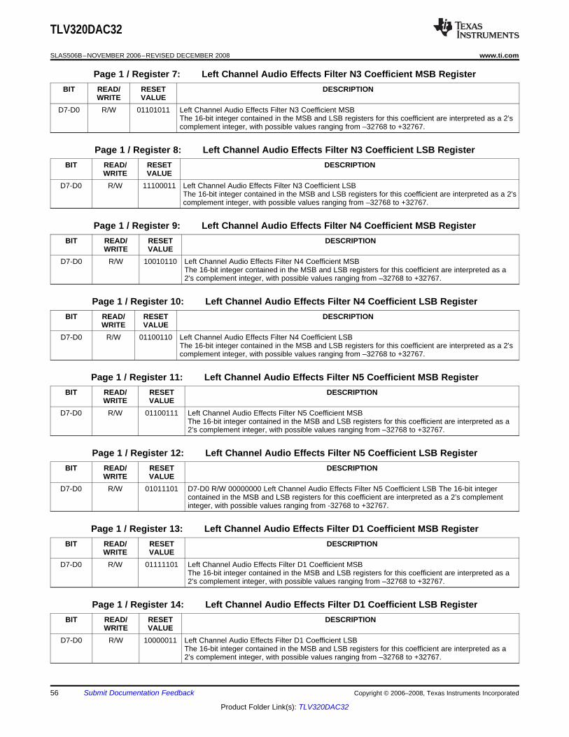
TLV320DAC32
SLAS506B–NOVEMBER 2006–REVISED DECEMBER 2008........................................................................................................................................ www.ti.com
Page 1 / Register 7: Left Channel Audio Effects Filter N3 Coefficient MSB RegisterBIT READ/ RESET DESCRIPTION
WRITE VALUED7-D0 R/W 01101011 Left Channel Audio Effects Filter N3 Coefficient MSB
The 16-bit integer contained in the MSB and LSB registers for this coefficient are interpreted as a 2’scomplement integer, with possible values ranging from –32768 to +32767.
Page 1 / Register 8: Left Channel Audio Effects Filter N3 Coefficient LSB RegisterBIT READ/ RESET DESCRIPTION
WRITE VALUED7-D0 R/W 11100011 Left Channel Audio Effects Filter N3 Coefficient LSB
The 16-bit integer contained in the MSB and LSB registers for this coefficient are interpreted as a 2’scomplement integer, with possible values ranging from –32768 to +32767.
Page 1 / Register 9: Left Channel Audio Effects Filter N4 Coefficient MSB RegisterBIT READ/ RESET DESCRIPTION
WRITE VALUED7-D0 R/W 10010110 Left Channel Audio Effects Filter N4 Coefficient MSB
The 16-bit integer contained in the MSB and LSB registers for this coefficient are interpreted as a2’s complement integer, with possible values ranging from –32768 to +32767.
Page 1 / Register 10: Left Channel Audio Effects Filter N4 Coefficient LSB RegisterBIT READ/ RESET DESCRIPTION
WRITE VALUED7-D0 R/W 01100110 Left Channel Audio Effects Filter N4 Coefficient LSB
The 16-bit integer contained in the MSB and LSB registers for this coefficient are interpreted as a 2’scomplement integer, with possible values ranging from –32768 to +32767.
Page 1 / Register 11: Left Channel Audio Effects Filter N5 Coefficient MSB RegisterBIT READ/ RESET DESCRIPTION
WRITE VALUED7-D0 R/W 01100111 Left Channel Audio Effects Filter N5 Coefficient MSB
The 16-bit integer contained in the MSB and LSB registers for this coefficient are interpreted as a2’s complement integer, with possible values ranging from –32768 to +32767.
Page 1 / Register 12: Left Channel Audio Effects Filter N5 Coefficient LSB RegisterBIT READ/ RESET DESCRIPTION
WRITE VALUED7-D0 R/W 01011101 D7-D0 R/W 00000000 Left Channel Audio Effects Filter N5 Coefficient LSB The 16-bit integer
contained in the MSB and LSB registers for this coefficient are interpreted as a 2’s complementinteger, with possible values ranging from -32768 to +32767.
Page 1 / Register 13: Left Channel Audio Effects Filter D1 Coefficient MSB RegisterBIT READ/ RESET DESCRIPTION
WRITE VALUED7-D0 R/W 01111101 Left Channel Audio Effects Filter D1 Coefficient MSB
The 16-bit integer contained in the MSB and LSB registers for this coefficient are interpreted as a2’s complement integer, with possible values ranging from –32768 to +32767.
Page 1 / Register 14: Left Channel Audio Effects Filter D1 Coefficient LSB RegisterBIT READ/ RESET DESCRIPTION
WRITE VALUED7-D0 R/W 10000011 Left Channel Audio Effects Filter D1 Coefficient LSB
The 16-bit integer contained in the MSB and LSB registers for this coefficient are interpreted as a2’s complement integer, with possible values ranging from –32768 to +32767.
56 Submit Documentation Feedback Copyright © 2006–2008, Texas Instruments Incorporated
Product Folder Link(s): TLV320DAC32
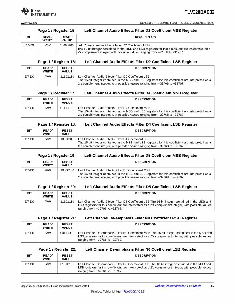
TLV320DAC32
www.ti.com........................................................................................................................................ SLAS506B–NOVEMBER 2006–REVISED DECEMBER 2008
Page 1 / Register 15: Left Channel Audio Effects Filter D2 Coefficient MSB RegisterBIT READ/ RESET DESCRIPTION
WRITE VALUED7-D0 R/W 10000100 Left Channel Audio Effects Filter D2 Coefficient MSB
The 16-bit integer contained in the MSB and LSB registers for this coefficient are interpreted as a2’s complement integer, with possible values ranging from –32768 to +32767.
Page 1 / Register 16: Left Channel Audio Effects Filter D2 Coefficient LSB RegisterBIT READ/ RESET DESCRIPTION
WRITE VALUED7-D0 R/W 11101110 Left Channel Audio Effects Filter D2 Coefficient LSB
The 16-bit integer contained in the MSB and LSB registers for this coefficient are interpreted as a2’s complement integer, with possible values ranging from –32768 to +32767.
Page 1 / Register 17: Left Channel Audio Effects Filter D4 Coefficient MSB RegisterBIT READ/ RESET DESCRIPTION
WRITE VALUED7-D0 R/W 01111101 Left Channel Audio Effects Filter D4 Coefficient MSB
The 16-bit integer contained in the MSB and LSB registers for this coefficient are interpreted as a2’s complement integer, with possible values ranging from –32768 to +32767.
Page 1 / Register 18: Left Channel Audio Effects Filter D4 Coefficient LSB RegisterBIT READ/ RESET DESCRIPTION
WRITE VALUED7-D0 R/W 10000011 Left Channel Audio Effects Filter D4 Coefficient LSB
The 16-bit integer contained in the MSB and LSB registers for this coefficient are interpreted as a2’s complement integer, with possible values ranging from –32768 to +32767.
Page 1 / Register 19: Left Channel Audio Effects Filter D5 Coefficient MSB RegisterBIT READ/ RESET DESCRIPTION
WRITE VALUED7-D0 R/W 10000100 Left Channel Audio Effects Filter D5 Coefficient MSB
The 16-bit integer contained in the MSB and LSB registers for this coefficient are interpreted as a2’s complement integer, with possible values ranging from –32768 to +32767.
Page 1 / Register 20: Left Channel Audio Effects Filter D5 Coefficient LSB RegisterBIT READ/ RESET DESCRIPTION
WRITE VALUED7-D0 R/W 11101110 Left Channel Audio Effects Filter D5 Coefficient LSB The 16-bit integer contained in the MSB and
LSB registers for this coefficient are interpreted as a 2’s complement integer, with possible valuesranging from –32768 to +32767.
Page 1 / Register 21: Left Channel De-emphasis Filter N0 Coefficient MSB RegisterBIT READ/ RESET DESCRIPTION
WRITE VALUED7-D0 R/W 00111001 Left Channel De-emphasis Filter N0 Coefficient MSB The 16-bit integer contained in the MSB and
LSB registers for this coefficient are interpreted as a 2’s complement integer, with possible valuesranging from –32768 to +32767.
Page 1 / Register 22: Left Channel De-emphasis Filter N0 Coefficient LSB RegisterBIT READ/ RESET DESCRIPTION
WRITE VALUED7-D0 R/W 01010101 Left Channel De-emphasis Filter N0 Coefficient LSB The 16-bit integer contained in the MSB and
LSB registers for this coefficient are interpreted as a 2’s complement integer, with possible valuesranging from –32768 to +32767.
Copyright © 2006–2008, Texas Instruments Incorporated Submit Documentation Feedback 57
Product Folder Link(s): TLV320DAC32
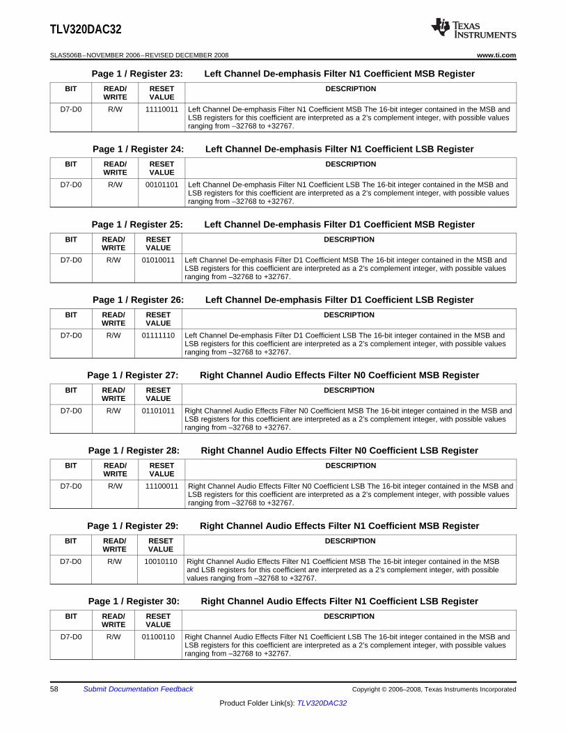
TLV320DAC32
SLAS506B–NOVEMBER 2006–REVISED DECEMBER 2008........................................................................................................................................ www.ti.com
Page 1 / Register 23: Left Channel De-emphasis Filter N1 Coefficient MSB RegisterBIT READ/ RESET DESCRIPTION
WRITE VALUED7-D0 R/W 11110011 Left Channel De-emphasis Filter N1 Coefficient MSB The 16-bit integer contained in the MSB and
LSB registers for this coefficient are interpreted as a 2’s complement integer, with possible valuesranging from –32768 to +32767.
Page 1 / Register 24: Left Channel De-emphasis Filter N1 Coefficient LSB RegisterBIT READ/ RESET DESCRIPTION
WRITE VALUED7-D0 R/W 00101101 Left Channel De-emphasis Filter N1 Coefficient LSB The 16-bit integer contained in the MSB and
LSB registers for this coefficient are interpreted as a 2’s complement integer, with possible valuesranging from –32768 to +32767.
Page 1 / Register 25: Left Channel De-emphasis Filter D1 Coefficient MSB RegisterBIT READ/ RESET DESCRIPTION
WRITE VALUED7-D0 R/W 01010011 Left Channel De-emphasis Filter D1 Coefficient MSB The 16-bit integer contained in the MSB and
LSB registers for this coefficient are interpreted as a 2’s complement integer, with possible valuesranging from –32768 to +32767.
Page 1 / Register 26: Left Channel De-emphasis Filter D1 Coefficient LSB RegisterBIT READ/ RESET DESCRIPTION
WRITE VALUED7-D0 R/W 01111110 Left Channel De-emphasis Filter D1 Coefficient LSB The 16-bit integer contained in the MSB and
LSB registers for this coefficient are interpreted as a 2’s complement integer, with possible valuesranging from –32768 to +32767.
Page 1 / Register 27: Right Channel Audio Effects Filter N0 Coefficient MSB RegisterBIT READ/ RESET DESCRIPTION
WRITE VALUED7-D0 R/W 01101011 Right Channel Audio Effects Filter N0 Coefficient MSB The 16-bit integer contained in the MSB and
LSB registers for this coefficient are interpreted as a 2’s complement integer, with possible valuesranging from –32768 to +32767.
Page 1 / Register 28: Right Channel Audio Effects Filter N0 Coefficient LSB RegisterBIT READ/ RESET DESCRIPTION
WRITE VALUED7-D0 R/W 11100011 Right Channel Audio Effects Filter N0 Coefficient LSB The 16-bit integer contained in the MSB and
LSB registers for this coefficient are interpreted as a 2’s complement integer, with possible valuesranging from –32768 to +32767.
Page 1 / Register 29: Right Channel Audio Effects Filter N1 Coefficient MSB RegisterBIT READ/ RESET DESCRIPTION
WRITE VALUED7-D0 R/W 10010110 Right Channel Audio Effects Filter N1 Coefficient MSB The 16-bit integer contained in the MSB
and LSB registers for this coefficient are interpreted as a 2’s complement integer, with possiblevalues ranging from –32768 to +32767.
Page 1 / Register 30: Right Channel Audio Effects Filter N1 Coefficient LSB RegisterBIT READ/ RESET DESCRIPTION
WRITE VALUED7-D0 R/W 01100110 Right Channel Audio Effects Filter N1 Coefficient LSB The 16-bit integer contained in the MSB and
LSB registers for this coefficient are interpreted as a 2’s complement integer, with possible valuesranging from –32768 to +32767.
58 Submit Documentation Feedback Copyright © 2006–2008, Texas Instruments Incorporated
Product Folder Link(s): TLV320DAC32
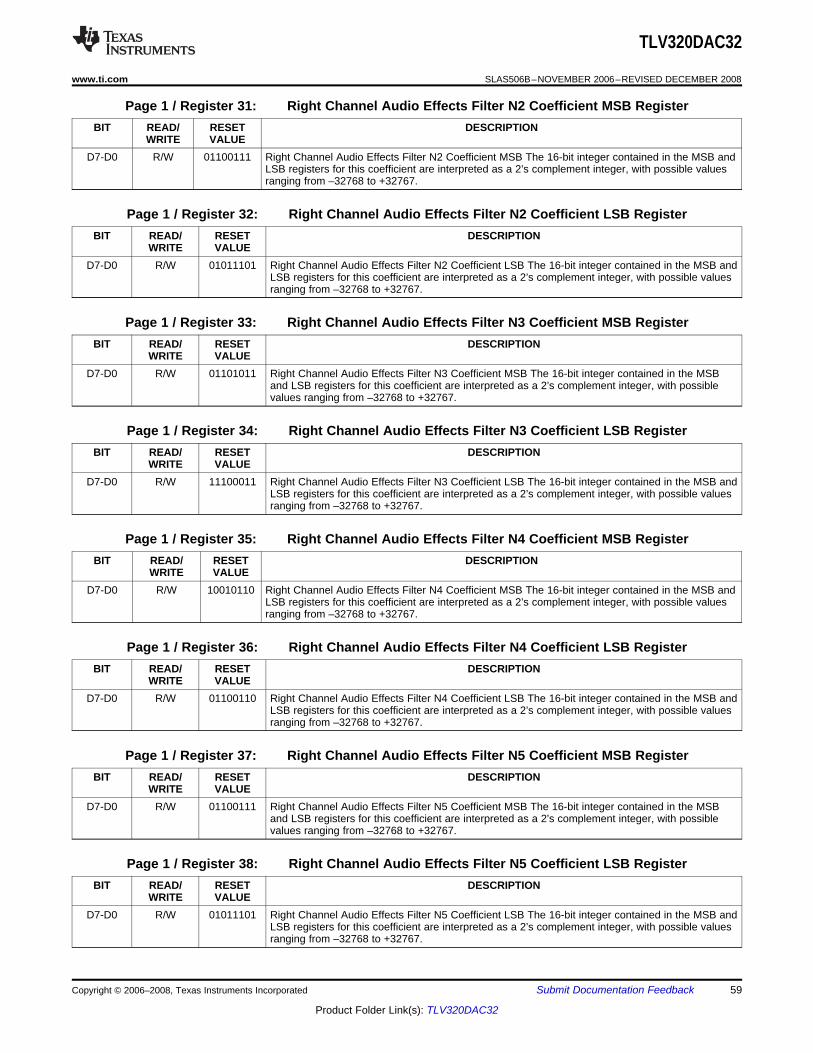
TLV320DAC32
www.ti.com........................................................................................................................................ SLAS506B–NOVEMBER 2006–REVISED DECEMBER 2008
Page 1 / Register 31: Right Channel Audio Effects Filter N2 Coefficient MSB RegisterBIT READ/ RESET DESCRIPTION
WRITE VALUED7-D0 R/W 01100111 Right Channel Audio Effects Filter N2 Coefficient MSB The 16-bit integer contained in the MSB and
LSB registers for this coefficient are interpreted as a 2’s complement integer, with possible valuesranging from –32768 to +32767.
Page 1 / Register 32: Right Channel Audio Effects Filter N2 Coefficient LSB RegisterBIT READ/ RESET DESCRIPTION
WRITE VALUED7-D0 R/W 01011101 Right Channel Audio Effects Filter N2 Coefficient LSB The 16-bit integer contained in the MSB and
LSB registers for this coefficient are interpreted as a 2’s complement integer, with possible valuesranging from –32768 to +32767.
Page 1 / Register 33: Right Channel Audio Effects Filter N3 Coefficient MSB RegisterBIT READ/ RESET DESCRIPTION
WRITE VALUED7-D0 R/W 01101011 Right Channel Audio Effects Filter N3 Coefficient MSB The 16-bit integer contained in the MSB
and LSB registers for this coefficient are interpreted as a 2’s complement integer, with possiblevalues ranging from –32768 to +32767.
Page 1 / Register 34: Right Channel Audio Effects Filter N3 Coefficient LSB RegisterBIT READ/ RESET DESCRIPTION
WRITE VALUED7-D0 R/W 11100011 Right Channel Audio Effects Filter N3 Coefficient LSB The 16-bit integer contained in the MSB and
LSB registers for this coefficient are interpreted as a 2’s complement integer, with possible valuesranging from –32768 to +32767.
Page 1 / Register 35: Right Channel Audio Effects Filter N4 Coefficient MSB RegisterBIT READ/ RESET DESCRIPTION
WRITE VALUED7-D0 R/W 10010110 Right Channel Audio Effects Filter N4 Coefficient MSB The 16-bit integer contained in the MSB and
LSB registers for this coefficient are interpreted as a 2’s complement integer, with possible valuesranging from –32768 to +32767.
Page 1 / Register 36: Right Channel Audio Effects Filter N4 Coefficient LSB RegisterBIT READ/ RESET DESCRIPTION
WRITE VALUED7-D0 R/W 01100110 Right Channel Audio Effects Filter N4 Coefficient LSB The 16-bit integer contained in the MSB and
LSB registers for this coefficient are interpreted as a 2’s complement integer, with possible valuesranging from –32768 to +32767.
Page 1 / Register 37: Right Channel Audio Effects Filter N5 Coefficient MSB RegisterBIT READ/ RESET DESCRIPTION
WRITE VALUED7-D0 R/W 01100111 Right Channel Audio Effects Filter N5 Coefficient MSB The 16-bit integer contained in the MSB
and LSB registers for this coefficient are interpreted as a 2’s complement integer, with possiblevalues ranging from –32768 to +32767.
Page 1 / Register 38: Right Channel Audio Effects Filter N5 Coefficient LSB RegisterBIT READ/ RESET DESCRIPTION
WRITE VALUED7-D0 R/W 01011101 Right Channel Audio Effects Filter N5 Coefficient LSB The 16-bit integer contained in the MSB and
LSB registers for this coefficient are interpreted as a 2’s complement integer, with possible valuesranging from –32768 to +32767.
Copyright © 2006–2008, Texas Instruments Incorporated Submit Documentation Feedback 59
Product Folder Link(s): TLV320DAC32
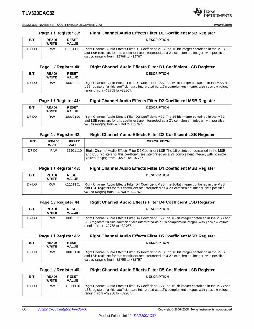
TLV320DAC32
SLAS506B–NOVEMBER 2006–REVISED DECEMBER 2008........................................................................................................................................ www.ti.com
Page 1 / Register 39: Right Channel Audio Effects Filter D1 Coefficient MSB RegisterBIT READ/ RESET DESCRIPTION
WRITE VALUED7-D0 R/W 01111101 Right Channel Audio Effects Filter D1 Coefficient MSB The 16-bit integer contained in the MSB
and LSB registers for this coefficient are interpreted as a 2’s complement integer, with possiblevalues ranging from –32768 to +32767.
Page 1 / Register 40: Right Channel Audio Effects Filter D1 Coefficient LSB RegisterBIT READ/ RESET DESCRIPTION
WRITE VALUED7-D0 R/W 10000011 Right Channel Audio Effects Filter D1 Coefficient LSB The 16-bit integer contained in the MSB and
LSB registers for this coefficient are interpreted as a 2’s complement integer, with possible valuesranging from –32768 to +32767.
Page 1 / Register 41: Right Channel Audio Effects Filter D2 Coefficient MSB RegisterBIT READ/ RESET DESCRIPTION
WRITE VALUED7-D0 R/W 10000100 Right Channel Audio Effects Filter D2 Coefficient MSB The 16-bit integer contained in the MSB
and LSB registers for this coefficient are interpreted as a 2’s complement integer, with possiblevalues ranging from –32768 to +32767.
Page 1 / Register 42: Right Channel Audio Effects Filter D2 Coefficient LSB RegisterBIT READ/ RESET DESCRIPTION
WRITE VALUED7-D0 R/W 11101110 Right Channel Audio Effects Filter D2 Coefficient LSB The 16-bit integer contained in the MSB
and LSB registers for this coefficient are interpreted as a 2’s complement integer, with possiblevalues ranging from –32768 to +32767.
Page 1 / Register 43: Right Channel Audio Effects Filter D4 Coefficient MSB RegisterBIT READ/ RESET DESCRIPTION
WRITE VALUED7-D0 R/W 01111101 Right Channel Audio Effects Filter D4 Coefficient MSB The 16-bit integer contained in the MSB
and LSB registers for this coefficient are interpreted as a 2’s complement integer, with possiblevalues ranging from –32768 to +32767.
Page 1 / Register 44: Right Channel Audio Effects Filter D4 Coefficient LSB RegisterBIT READ/ RESET DESCRIPTION
WRITE VALUED7-D0 R/W 10000011 Right Channel Audio Effects Filter D4 Coefficient LSB The 16-bit integer contained in the MSB and
LSB registers for this coefficient are interpreted as a 2’s complement integer, with possible valuesranging from –32768 to +32767.
Page 1 / Register 45: Right Channel Audio Effects Filter D5 Coefficient MSB RegisterBIT READ/ RESET DESCRIPTION
WRITE VALUED7-D0 R/W 10000100 Right Channel Audio Effects Filter D5 Coefficient MSB The 16-bit integer contained in the MSB
and LSB registers for this coefficient are interpreted as a 2’s complement integer, with possiblevalues ranging from –32768 to +32767.
Page 1 / Register 46: Right Channel Audio Effects Filter D5 Coefficient LSB RegisterBIT READ/ RESET DESCRIPTION
WRITE VALUED7-D0 R/W 11101110 Right Channel Audio Effects Filter D5 Coefficient LSB The 16-bit integer contained in the MSB and
LSB registers for this coefficient are interpreted as a 2’s complement integer, with possible valuesranging from –32768 to +32767.
60 Submit Documentation Feedback Copyright © 2006–2008, Texas Instruments Incorporated
Product Folder Link(s): TLV320DAC32
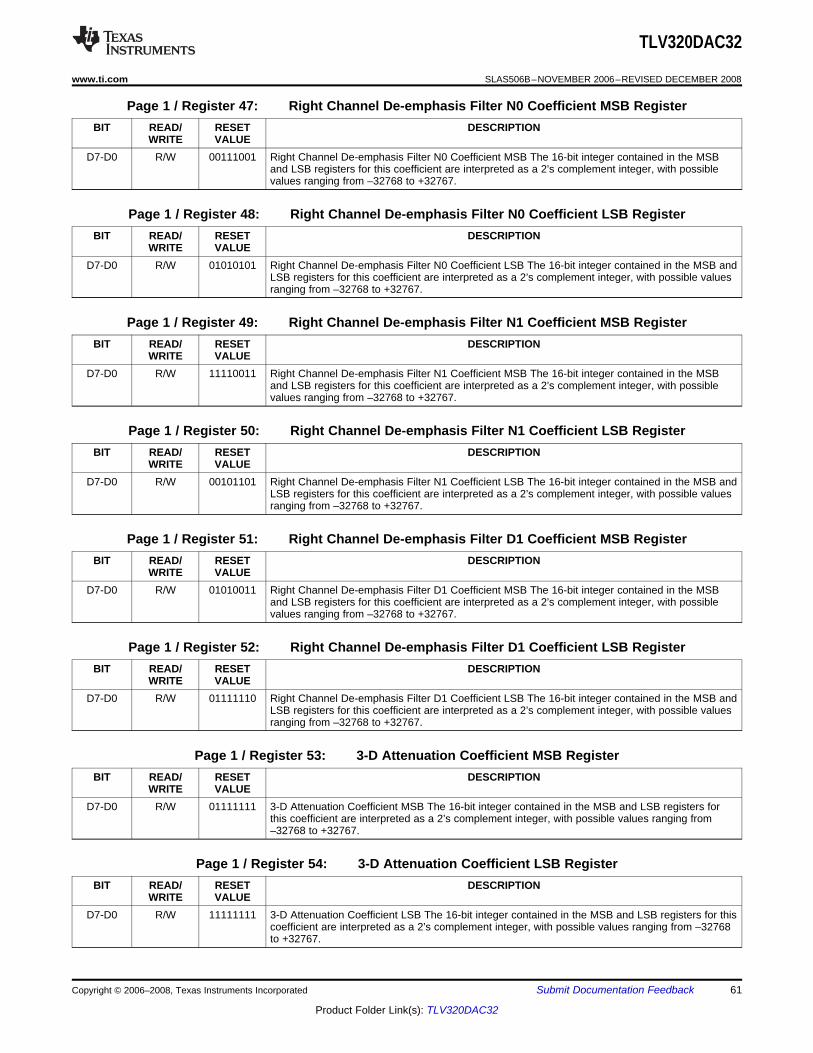
TLV320DAC32
www.ti.com........................................................................................................................................ SLAS506B–NOVEMBER 2006–REVISED DECEMBER 2008
Page 1 / Register 47: Right Channel De-emphasis Filter N0 Coefficient MSB RegisterBIT READ/ RESET DESCRIPTION
WRITE VALUED7-D0 R/W 00111001 Right Channel De-emphasis Filter N0 Coefficient MSB The 16-bit integer contained in the MSB
and LSB registers for this coefficient are interpreted as a 2’s complement integer, with possiblevalues ranging from –32768 to +32767.
Page 1 / Register 48: Right Channel De-emphasis Filter N0 Coefficient LSB RegisterBIT READ/ RESET DESCRIPTION
WRITE VALUED7-D0 R/W 01010101 Right Channel De-emphasis Filter N0 Coefficient LSB The 16-bit integer contained in the MSB and
LSB registers for this coefficient are interpreted as a 2’s complement integer, with possible valuesranging from –32768 to +32767.
Page 1 / Register 49: Right Channel De-emphasis Filter N1 Coefficient MSB RegisterBIT READ/ RESET DESCRIPTION
WRITE VALUED7-D0 R/W 11110011 Right Channel De-emphasis Filter N1 Coefficient MSB The 16-bit integer contained in the MSB
and LSB registers for this coefficient are interpreted as a 2’s complement integer, with possiblevalues ranging from –32768 to +32767.
Page 1 / Register 50: Right Channel De-emphasis Filter N1 Coefficient LSB RegisterBIT READ/ RESET DESCRIPTION
WRITE VALUED7-D0 R/W 00101101 Right Channel De-emphasis Filter N1 Coefficient LSB The 16-bit integer contained in the MSB and
LSB registers for this coefficient are interpreted as a 2’s complement integer, with possible valuesranging from –32768 to +32767.
Page 1 / Register 51: Right Channel De-emphasis Filter D1 Coefficient MSB RegisterBIT READ/ RESET DESCRIPTION
WRITE VALUED7-D0 R/W 01010011 Right Channel De-emphasis Filter D1 Coefficient MSB The 16-bit integer contained in the MSB
and LSB registers for this coefficient are interpreted as a 2’s complement integer, with possiblevalues ranging from –32768 to +32767.
Page 1 / Register 52: Right Channel De-emphasis Filter D1 Coefficient LSB RegisterBIT READ/ RESET DESCRIPTION
WRITE VALUED7-D0 R/W 01111110 Right Channel De-emphasis Filter D1 Coefficient LSB The 16-bit integer contained in the MSB and
LSB registers for this coefficient are interpreted as a 2’s complement integer, with possible valuesranging from –32768 to +32767.
Page 1 / Register 53: 3-D Attenuation Coefficient MSB RegisterBIT READ/ RESET DESCRIPTION
WRITE VALUED7-D0 R/W 01111111 3-D Attenuation Coefficient MSB The 16-bit integer contained in the MSB and LSB registers for
this coefficient are interpreted as a 2’s complement integer, with possible values ranging from–32768 to +32767.
Page 1 / Register 54: 3-D Attenuation Coefficient LSB RegisterBIT READ/ RESET DESCRIPTION
WRITE VALUED7-D0 R/W 11111111 3-D Attenuation Coefficient LSB The 16-bit integer contained in the MSB and LSB registers for this
coefficient are interpreted as a 2’s complement integer, with possible values ranging from –32768to +32767.
Copyright © 2006–2008, Texas Instruments Incorporated Submit Documentation Feedback 61
Product Folder Link(s): TLV320DAC32
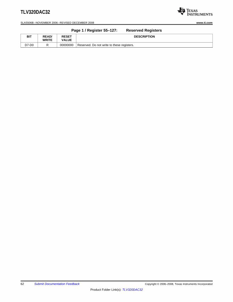
TLV320DAC32
SLAS506B–NOVEMBER 2006–REVISED DECEMBER 2008........................................................................................................................................ www.ti.com
Page 1 / Register 55–127: Reserved RegistersBIT READ/ RESET DESCRIPTION
WRITE VALUED7-D0 R 00000000 Reserved. Do not write to these registers.
62 Submit Documentation Feedback Copyright © 2006–2008, Texas Instruments Incorporated
Product Folder Link(s): TLV320DAC32
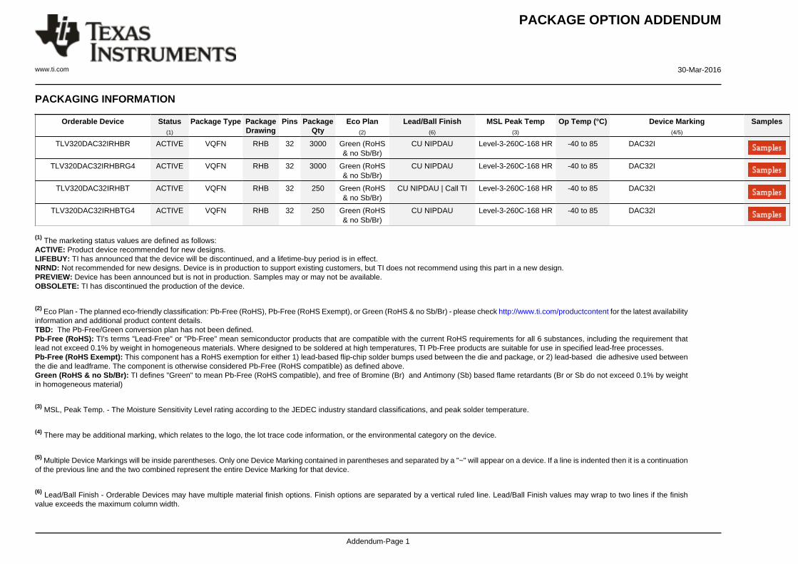
PACKAGE OPTION ADDENDUM
www.ti.com 30-Mar-2016
Addendum-Page 1
PACKAGING INFORMATION
Orderable Device Status(1)
Package Type PackageDrawing
Pins PackageQty
Eco Plan(2)
Lead/Ball Finish(6)
MSL Peak Temp(3)
Op Temp (°C) Device Marking(4/5)
Samples
TLV320DAC32IRHBR ACTIVE VQFN RHB 32 3000 Green (RoHS& no Sb/Br)
CU NIPDAU Level-3-260C-168 HR -40 to 85 DAC32I
TLV320DAC32IRHBRG4 ACTIVE VQFN RHB 32 3000 Green (RoHS& no Sb/Br)
CU NIPDAU Level-3-260C-168 HR -40 to 85 DAC32I
TLV320DAC32IRHBT ACTIVE VQFN RHB 32 250 Green (RoHS& no Sb/Br)
CU NIPDAU | Call TI Level-3-260C-168 HR -40 to 85 DAC32I
TLV320DAC32IRHBTG4 ACTIVE VQFN RHB 32 250 Green (RoHS& no Sb/Br)
CU NIPDAU Level-3-260C-168 HR -40 to 85 DAC32I
(1) The marketing status values are defined as follows:ACTIVE: Product device recommended for new designs.LIFEBUY: TI has announced that the device will be discontinued, and a lifetime-buy period is in effect.NRND: Not recommended for new designs. Device is in production to support existing customers, but TI does not recommend using this part in a new design.PREVIEW: Device has been announced but is not in production. Samples may or may not be available.OBSOLETE: TI has discontinued the production of the device.
(2) Eco Plan - The planned eco-friendly classification: Pb-Free (RoHS), Pb-Free (RoHS Exempt), or Green (RoHS & no Sb/Br) - please check http://www.ti.com/productcontent for the latest availabilityinformation and additional product content details.TBD: The Pb-Free/Green conversion plan has not been defined.Pb-Free (RoHS): TI's terms "Lead-Free" or "Pb-Free" mean semiconductor products that are compatible with the current RoHS requirements for all 6 substances, including the requirement thatlead not exceed 0.1% by weight in homogeneous materials. Where designed to be soldered at high temperatures, TI Pb-Free products are suitable for use in specified lead-free processes.Pb-Free (RoHS Exempt): This component has a RoHS exemption for either 1) lead-based flip-chip solder bumps used between the die and package, or 2) lead-based die adhesive used betweenthe die and leadframe. The component is otherwise considered Pb-Free (RoHS compatible) as defined above.Green (RoHS & no Sb/Br): TI defines "Green" to mean Pb-Free (RoHS compatible), and free of Bromine (Br) and Antimony (Sb) based flame retardants (Br or Sb do not exceed 0.1% by weightin homogeneous material)
(3) MSL, Peak Temp. - The Moisture Sensitivity Level rating according to the JEDEC industry standard classifications, and peak solder temperature.
(4) There may be additional marking, which relates to the logo, the lot trace code information, or the environmental category on the device.
(5) Multiple Device Markings will be inside parentheses. Only one Device Marking contained in parentheses and separated by a "~" will appear on a device. If a line is indented then it is a continuationof the previous line and the two combined represent the entire Device Marking for that device.
(6) Lead/Ball Finish - Orderable Devices may have multiple material finish options. Finish options are separated by a vertical ruled line. Lead/Ball Finish values may wrap to two lines if the finishvalue exceeds the maximum column width.
PACKAGE OPTION ADDENDUM
www.ti.com 30-Mar-2016
Addendum-Page 2
Important Information and Disclaimer:The information provided on this page represents TI's knowledge and belief as of the date that it is provided. TI bases its knowledge and belief on informationprovided by third parties, and makes no representation or warranty as to the accuracy of such information. Efforts are underway to better integrate information from third parties. TI has taken andcontinues to take reasonable steps to provide representative and accurate information but may not have conducted destructive testing or chemical analysis on incoming materials and chemicals.TI and TI suppliers consider certain information to be proprietary, and thus CAS numbers and other limited information may not be available for release.
In no event shall TI's liability arising out of such information exceed the total purchase price of the TI part(s) at issue in this document sold by TI to Customer on an annual basis.
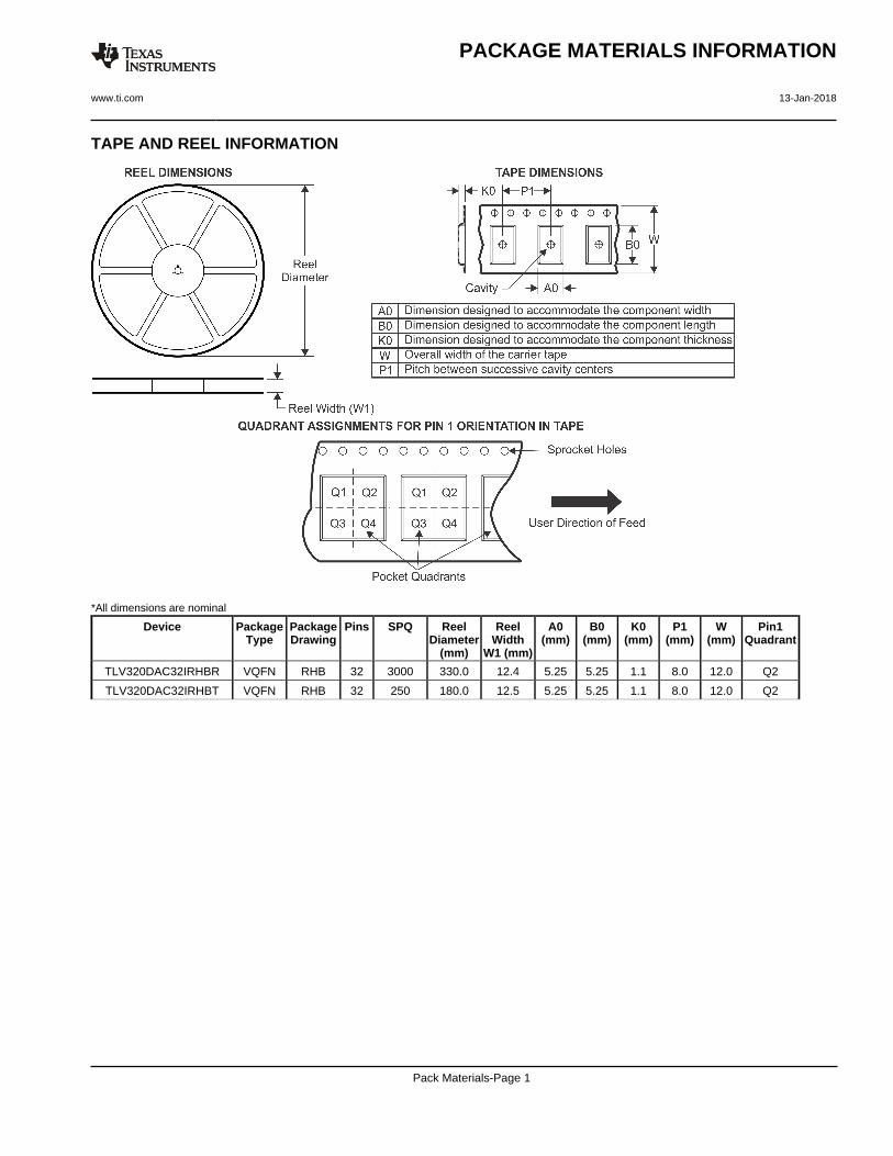
TAPE AND REEL INFORMATION
*All dimensions are nominal
Device PackageType
PackageDrawing
Pins SPQ ReelDiameter
(mm)
ReelWidth
W1 (mm)
A0(mm)
B0(mm)
K0(mm)
P1(mm)
W(mm)
Pin1Quadrant
TLV320DAC32IRHBR VQFN RHB 32 3000 330.0 12.4 5.25 5.25 1.1 8.0 12.0 Q2
TLV320DAC32IRHBT VQFN RHB 32 250 180.0 12.5 5.25 5.25 1.1 8.0 12.0 Q2
PACKAGE MATERIALS INFORMATION
www.ti.com 13-Jan-2018
Pack Materials-Page 1
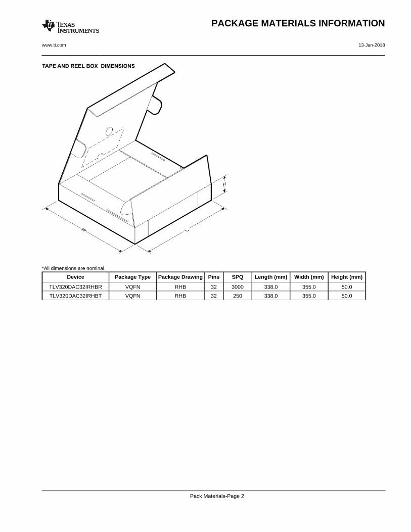
*All dimensions are nominal
Device Package Type Package Drawing Pins SPQ Length (mm) Width (mm) Height (mm)
TLV320DAC32IRHBR VQFN RHB 32 3000 338.0 355.0 50.0
TLV320DAC32IRHBT VQFN RHB 32 250 338.0 355.0 50.0
PACKAGE MATERIALS INFORMATION
www.ti.com 13-Jan-2018
Pack Materials-Page 2
IMPORTANT NOTICE
Texas Instruments Incorporated (TI) reserves the right to make corrections, enhancements, improvements and other changes to itssemiconductor products and services per JESD46, latest issue, and to discontinue any product or service per JESD48, latest issue. Buyersshould obtain the latest relevant information before placing orders and should verify that such information is current and complete.TI’s published terms of sale for semiconductor products (http://www.ti.com/sc/docs/stdterms.htm) apply to the sale of packaged integratedcircuit products that TI has qualified and released to market. Additional terms may apply to the use or sale of other types of TI products andservices.Reproduction of significant portions of TI information in TI data sheets is permissible only if reproduction is without alteration and isaccompanied by all associated warranties, conditions, limitations, and notices. TI is not responsible or liable for such reproduceddocumentation. Information of third parties may be subject to additional restrictions. Resale of TI products or services with statementsdifferent from or beyond the parameters stated by TI for that product or service voids all express and any implied warranties for theassociated TI product or service and is an unfair and deceptive business practice. TI is not responsible or liable for any such statements.Buyers and others who are developing systems that incorporate TI products (collectively, “Designers”) understand and agree that Designersremain responsible for using their independent analysis, evaluation and judgment in designing their applications and that Designers havefull and exclusive responsibility to assure the safety of Designers' applications and compliance of their applications (and of all TI productsused in or for Designers’ applications) with all applicable regulations, laws and other applicable requirements. Designer represents that, withrespect to their applications, Designer has all the necessary expertise to create and implement safeguards that (1) anticipate dangerousconsequences of failures, (2) monitor failures and their consequences, and (3) lessen the likelihood of failures that might cause harm andtake appropriate actions. Designer agrees that prior to using or distributing any applications that include TI products, Designer willthoroughly test such applications and the functionality of such TI products as used in such applications.TI’s provision of technical, application or other design advice, quality characterization, reliability data or other services or information,including, but not limited to, reference designs and materials relating to evaluation modules, (collectively, “TI Resources”) are intended toassist designers who are developing applications that incorporate TI products; by downloading, accessing or using TI Resources in anyway, Designer (individually or, if Designer is acting on behalf of a company, Designer’s company) agrees to use any particular TI Resourcesolely for this purpose and subject to the terms of this Notice.TI’s provision of TI Resources does not expand or otherwise alter TI’s applicable published warranties or warranty disclaimers for TIproducts, and no additional obligations or liabilities arise from TI providing such TI Resources. TI reserves the right to make corrections,enhancements, improvements and other changes to its TI Resources. TI has not conducted any testing other than that specificallydescribed in the published documentation for a particular TI Resource.Designer is authorized to use, copy and modify any individual TI Resource only in connection with the development of applications thatinclude the TI product(s) identified in such TI Resource. NO OTHER LICENSE, EXPRESS OR IMPLIED, BY ESTOPPEL OR OTHERWISETO ANY OTHER TI INTELLECTUAL PROPERTY RIGHT, AND NO LICENSE TO ANY TECHNOLOGY OR INTELLECTUAL PROPERTYRIGHT OF TI OR ANY THIRD PARTY IS GRANTED HEREIN, including but not limited to any patent right, copyright, mask work right, orother intellectual property right relating to any combination, machine, or process in which TI products or services are used. Informationregarding or referencing third-party products or services does not constitute a license to use such products or services, or a warranty orendorsement thereof. Use of TI Resources may require a license from a third party under the patents or other intellectual property of thethird party, or a license from TI under the patents or other intellectual property of TI.TI RESOURCES ARE PROVIDED “AS IS” AND WITH ALL FAULTS. TI DISCLAIMS ALL OTHER WARRANTIES ORREPRESENTATIONS, EXPRESS OR IMPLIED, REGARDING RESOURCES OR USE THEREOF, INCLUDING BUT NOT LIMITED TOACCURACY OR COMPLETENESS, TITLE, ANY EPIDEMIC FAILURE WARRANTY AND ANY IMPLIED WARRANTIES OFMERCHANTABILITY, FITNESS FOR A PARTICULAR PURPOSE, AND NON-INFRINGEMENT OF ANY THIRD PARTY INTELLECTUALPROPERTY RIGHTS. TI SHALL NOT BE LIABLE FOR AND SHALL NOT DEFEND OR INDEMNIFY DESIGNER AGAINST ANY CLAIM,INCLUDING BUT NOT LIMITED TO ANY INFRINGEMENT CLAIM THAT RELATES TO OR IS BASED ON ANY COMBINATION OFPRODUCTS EVEN IF DESCRIBED IN TI RESOURCES OR OTHERWISE. IN NO EVENT SHALL TI BE LIABLE FOR ANY ACTUAL,DIRECT, SPECIAL, COLLATERAL, INDIRECT, PUNITIVE, INCIDENTAL, CONSEQUENTIAL OR EXEMPLARY DAMAGES INCONNECTION WITH OR ARISING OUT OF TI RESOURCES OR USE THEREOF, AND REGARDLESS OF WHETHER TI HAS BEENADVISED OF THE POSSIBILITY OF SUCH DAMAGES.Unless TI has explicitly designated an individual product as meeting the requirements of a particular industry standard (e.g., ISO/TS 16949and ISO 26262), TI is not responsible for any failure to meet such industry standard requirements.Where TI specifically promotes products as facilitating functional safety or as compliant with industry functional safety standards, suchproducts are intended to help enable customers to design and create their own applications that meet applicable functional safety standardsand requirements. Using products in an application does not by itself establish any safety features in the application. Designers mustensure compliance with safety-related requirements and standards applicable to their applications. Designer may not use any TI products inlife-critical medical equipment unless authorized officers of the parties have executed a special contract specifically governing such use.Life-critical medical equipment is medical equipment where failure of such equipment would cause serious bodily injury or death (e.g., lifesupport, pacemakers, defibrillators, heart pumps, neurostimulators, and implantables). Such equipment includes, without limitation, allmedical devices identified by the U.S. Food and Drug Administration as Class III devices and equivalent classifications outside the U.S.TI may expressly designate certain products as completing a particular qualification (e.g., Q100, Military Grade, or Enhanced Product).Designers agree that it has the necessary expertise to select the product with the appropriate qualification designation for their applicationsand that proper product selection is at Designers’ own risk. Designers are solely responsible for compliance with all legal and regulatoryrequirements in connection with such selection.Designer will fully indemnify TI and its representatives against any damages, costs, losses, and/or liabilities arising out of Designer’s non-compliance with the terms and provisions of this Notice.
Mailing Address: Texas Instruments, Post Office Box 655303, Dallas, Texas 75265Copyright © 2018, Texas Instruments Incorporated