Embed Size (px)
Citation preview
15 MHz Rail-to-RailOperational Amplifiers
OP162/OP262/OP462
Rev. F Information furnished by Analog Devices is believed to be accurate and reliable. However, no responsibility is assumed by Analog Devices for its use, nor for any infringements of patents or other rights of third parties that may result from its use. Specifications subject to change without notice. No license is granted by implication or otherwise under any patent or patent rights of Analog Devices. Trademarks and registered trademarks are the property of their respective owners.
One Technology Way, P.O. Box 9106, Norwood, MA 02062-9106, U.S.A. Tel: 781.329.4700 www.analog.com Fax: 781.326.8703 © 2005 Analog Devices, Inc. All rights reserved.
FEATURES Wide bandwidth: 15 MHz Low offset voltage: 325 µV max
Low noise: 9.5 nV/√Hz @ 1 kHz Single-supply operation: 2.7 V to 12 V Rail-to-rail output swing Low TCVOS: 1 µV/°C typ High slew rate: 13 V/µs No phase inversion Unity-gain stable
APPLICATIONS Portable instrumentation Sampling ADC amplifier Wireless LANs Direct access arrangement Office automation
GENERAL DESCRIPTION
The OP162 (single), OP262 (dual), and OP462 (quad) rail-to-rail 15 MHz amplifiers feature the extra speed new designs require, with the benefits of precision and low power operation. With their incredibly low offset voltage of 45 µV (typical) and low noise, they are perfectly suited for precision filter applica-tions and instrumentation. The low supply current of 500 µA (typical) is critical for portable or densely packed designs. In addition, the rail-to-rail output swing provides greater dynamic range and control than standard video amplifiers.
These products operate from single supplies as low as 2.7 V to dual supplies of ±6 V. The fast settling times and wide output swings recommend them for buffers to sampling A/D converters. The output drive of 30 mA (sink and source) is needed for many audio and display applications; more output current can be supplied for limited durations. The OPx62 family is specified over the extended industrial temperature range (–40°C to +125°C). The single OP162 amplifiers are available in 8-lead SOIC, MSOP, and TSSOP packages. The dual OP262 amplifiers are available in 8-lead SOIC and TSSOP packages. The quad OP462 amplifiers are available in 14-lead, narrow-body SOIC and TSSOP packages.
PIN CONFIGURATIONS
NULL 1
–IN A 2
+IN A 3
V– 4
NULL8
V+7
OUT A6
NC5
NC = NO CONNECT
OP162TOP VIEW
(Not to Scale)
0028
8-00
1
Figure 1. 8-Lead Narrow-Body SOIC (S Suffix)
TOP VIEW(Not to Scale)
1
2
3
4
OP162–IN A
+IN A
V–
NULL 8
7
6
5
V+
OUT A
NC
NULL
NC = NO CONNECT 0028
8-00
2
Figure 2. 8-Lead TSSOP (RU Suffix) 8-Lead MSOP (RM Suffix)
OUT A 1
–IN A 2
+IN A 3
V– 4
V+8
OUT B7
–IN B6
+IN B5
OP262TOP VIEW
(Not to Scale)
0028
8-00
3
Figure 3. 8-Lead Narrow-Body SOIC (S Suffix)
TOP VIEW(Not to Scale)
1
2
3
4
OP262–IN A
+IN A
V–
OUT A 8
7
6
5
OUT B
–IN B
+IN B
V+
0028
8-00
4
Figure 4. 8-Lead TSSOP (RU Suffix)
OUT A 1
–IN A 2
+IN A 3
V+ 4
OUT D14
–IN D13
+IN D12
V–11
+IN B 5 +IN C10
–IN B 6 –IN C9
OUT B 7 OUT C8
OP462TOP VIEW
(Not to Scale)
0028
8-00
5
Figure 5. 14-Lead Narrow-Body SOIC (S Suffix)
1
2
3
4
5
6
7
OP462
–IN A
+IN A
V+
OUT B
–IN B
+IN B
OUT A 14
13
12
11
10
9
8
–IN D
+IN D
V–
OUT C
–IN C
+IN C
OUT D
TOP VIEW(Not to Scale)
0028
8-00
6
Figure 6. 14-Lead TSSOP (RU Suffix)
www.BDTIC.com/ADI
OP162/OP262/OP462
Rev. F | Page 2 of 20
TABLE OF CONTENTS Specifications...........................................................................................3 Absolute Maximum Ratings.................................................................6
ESD Caution.................................................................................. 6 Typical Performance Characteristics ..................................................7 Applications ...........................................................................................12
Functional Description.............................................................. 12
Offset Adjustment ...................................................................... 12
Rail-to-Rail Output .................................................................... 12
Output Short-Circuit Protection.............................................. 12
Input Overvoltage Protection ................................................... 13
Output Phase Reversal ............................................................... 13
Power Dissipation....................................................................... 13
Unused Amplifiers ..................................................................... 14
Power-On Settling Time............................................................ 14
Capacitive Load Drive ............................................................... 14
Total Harmonic Distortion and Crosstalk .............................. 15
PCB Layout Considerations...................................................... 15 Application Circuits ............................................................................ 16
Single-Supply Stereo Headphone Driver................................. 16
Instrumentation Amplifier........................................................ 16
Direct Access Arrangement ...................................................... 17
Spice Macro-Model .................................................................... 18 Outline Dimensions ............................................................................ 19
Ordering Guide .......................................................................... 20
REVISION HISTORY 1/05—Rev. E to Rev. F Changes to Absolute Maximum Ratings Table 4 and Table 5 .... 6 Change to Figure 36 ....................................................................... 13 Changes to Ordering Guide .......................................................... 20 12/04—Rev. D to Rev. E Updated Format..................................................................Universal Changes to General Description .................................................... 1 Changes to Specifications ................................................................ 3 Changes to Package Type................................................................. 6 Change to Figure 16 ......................................................................... 8 Change to Figure 22 ......................................................................... 9 Change to Figure 36 ....................................................................... 13 Change to Figure 37 ....................................................................... 14 Changes to Ordering Guide .......................................................... 20 10/02—Rev. C to Rev. D Deleted 8-Lead Plastic DIP (N-8) ....................................Universal Deleted 14-Lead Plastic DIP (N-14) ................................Universal Edits to ORDERING GUIDE........................................................ 19 Edits to Figure 30............................................................................ 19 Edits to Figure 31............................................................................ 19 Updated Outline Dimensions ....................................................... 19
www.BDTIC.com/ADI
OP162/OP262/OP462
Rev. F | Page 3 of 20
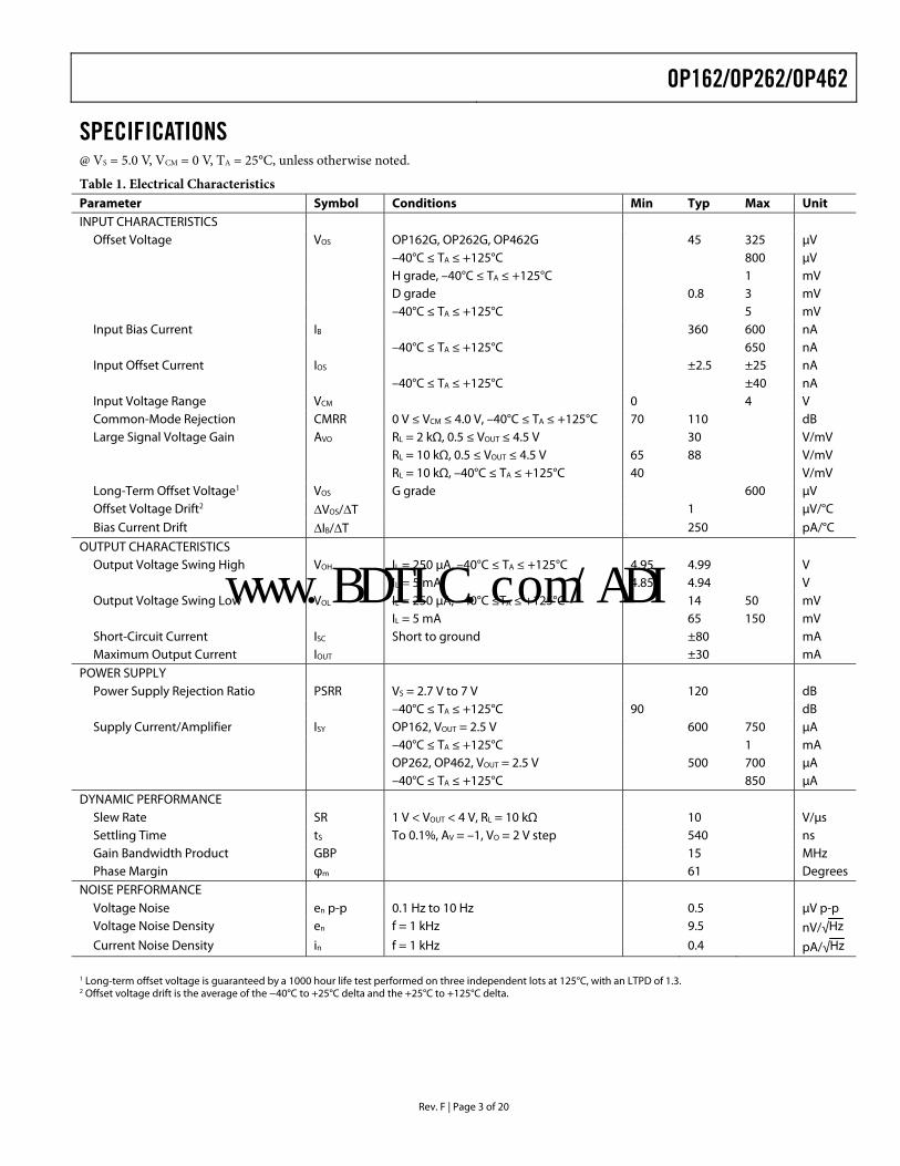
SPECIFICATIONS @ VS = 5.0 V, VCM = 0 V, TA = 25°C, unless otherwise noted.
Table 1. Electrical Characteristics Parameter Symbol Conditions Min Typ Max Unit INPUT CHARACTERISTICS
Offset Voltage VOS OP162G, OP262G, OP462G 45 325 µV –40°C ≤ TA ≤ +125°C 800 µV H grade, –40°C ≤ TA ≤ +125°C 1 mV D grade 0.8 3 mV –40°C ≤ TA ≤ +125°C 5 mV Input Bias Current IB 360 600 nA –40°C ≤ TA ≤ +125°C 650 nA Input Offset Current IOS ±2.5 ±25 nA –40°C ≤ TA ≤ +125°C ±40 nA Input Voltage Range VCM 0 4 V Common-Mode Rejection CMRR 0 V ≤ VCM ≤ 4.0 V, –40°C ≤ TA ≤ +125°C 70 110 dB Large Signal Voltage Gain AVO RL = 2 kΩ, 0.5 ≤ VOUT ≤ 4.5 V 30 V/mV RL = 10 kΩ, 0.5 ≤ VOUT ≤ 4.5 V 65 88 V/mV RL = 10 kΩ, –40°C ≤ TA ≤ +125°C 40 V/mV Long-Term Offset Voltage1 VOS G grade 600 µV Offset Voltage Drift2 ∆VOS/∆T 1 µV/°C Bias Current Drift ∆IB/∆T 250 pA/°C
OUTPUT CHARACTERISTICS Output Voltage Swing High VOH IL = 250 µA, –40°C ≤ TA ≤ +125°C 4.95 4.99 V IL = 5 mA 4.85 4.94 V Output Voltage Swing Low VOL IL = 250 µA, –40°C ≤TA ≤ +125°C 14 50 mV IL = 5 mA 65 150 mV Short-Circuit Current ISC Short to ground ±80 mA Maximum Output Current IOUT ±30 mA
POWER SUPPLY Power Supply Rejection Ratio PSRR VS = 2.7 V to 7 V 120 dB –40°C ≤ TA ≤ +125°C 90 dB Supply Current/Amplifier ISY OP162, VOUT = 2.5 V 600 750 µA
–40°C ≤ TA ≤ +125°C 1 mA OP262, OP462, VOUT = 2.5 V 500 700 µA –40°C ≤ TA ≤ +125°C 850 µA DYNAMIC PERFORMANCE
Slew Rate SR 1 V < VOUT < 4 V, RL = 10 kΩ 10 V/µs Settling Time tS To 0.1%, AV = –1, VO = 2 V step 540 ns Gain Bandwidth Product GBP 15 MHz Phase Margin φm 61 Degrees
NOISE PERFORMANCE Voltage Noise en p-p 0.1 Hz to 10 Hz 0.5 µV p-p Voltage Noise Density en f = 1 kHz 9.5 nV/√Hz
Current Noise Density in f = 1 kHz 0.4 pA/√Hz
1 Long-term offset voltage is guaranteed by a 1000 hour life test performed on three independent lots at 125°C, with an LTPD of 1.3. 2 Offset voltage drift is the average of the −40°C to +25°C delta and the +25°C to +125°C delta.
www.BDTIC.com/ADI
OP162/OP262/OP462
Rev. F | Page 4 of 20
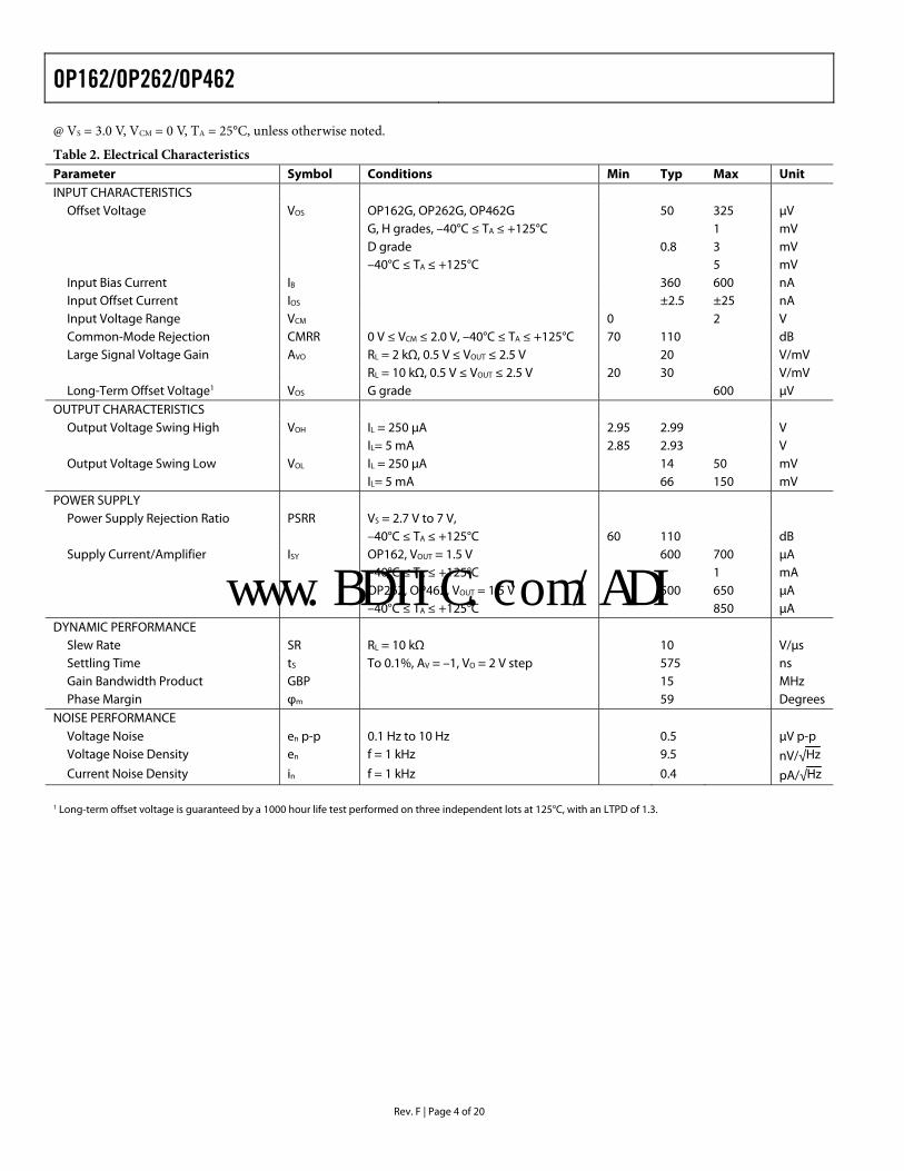
@ VS = 3.0 V, VCM = 0 V, TA = 25°C, unless otherwise noted.
Table 2. Electrical Characteristics Parameter Symbol Conditions Min Typ Max Unit INPUT CHARACTERISTICS
Offset Voltage VOS OP162G, OP262G, OP462G 50 325 µV G, H grades, –40°C ≤ TA ≤ +125°C 1 mV D grade 0.8 3 mV –40°C ≤ TA ≤ +125°C 5 mV Input Bias Current IB 360 600 nA Input Offset Current IOS ±2.5 ±25 nA Input Voltage Range VCM 0 2 V Common-Mode Rejection CMRR 0 V ≤ VCM ≤ 2.0 V, –40°C ≤ TA ≤ +125°C 70 110 dB Large Signal Voltage Gain AVO RL = 2 kΩ, 0.5 V ≤ VOUT ≤ 2.5 V 20 V/mV RL = 10 kΩ, 0.5 V ≤ VOUT ≤ 2.5 V 20 30 V/mV Long-Term Offset Voltage1 VOS G grade 600 µV
OUTPUT CHARACTERISTICS Output Voltage Swing High VOH IL = 250 µA 2.95 2.99 V IL= 5 mA 2.85 2.93 V Output Voltage Swing Low VOL IL = 250 µA 14 50 mV
IL= 5 mA 66 150 mV POWER SUPPLY
Power Supply Rejection Ratio PSRR VS = 2.7 V to 7 V, –40°C ≤ TA ≤ +125°C 60 110 dB Supply Current/Amplifier ISY OP162, VOUT = 1.5 V 600 700 µA
–40°C ≤ TA ≤ +125°C 1 mA OP262, OP462, VOUT = 1.5 V 500 650 µA –40°C ≤ TA ≤ +125°C 850 µA DYNAMIC PERFORMANCE
Slew Rate SR RL = 10 kΩ 10 V/µs Settling Time tS To 0.1%, AV = –1, VO = 2 V step 575 ns Gain Bandwidth Product GBP 15 MHz Phase Margin φm 59 Degrees
NOISE PERFORMANCE Voltage Noise en p-p 0.1 Hz to 10 Hz 0.5 µV p-p Voltage Noise Density en f = 1 kHz 9.5 nV/√Hz
Current Noise Density in f = 1 kHz 0.4 pA/√Hz
1 Long-term offset voltage is guaranteed by a 1000 hour life test performed on three independent lots at 125°C, with an LTPD of 1.3.
www.BDTIC.com/ADI
OP162/OP262/OP462
Rev. F | Page 5 of 20
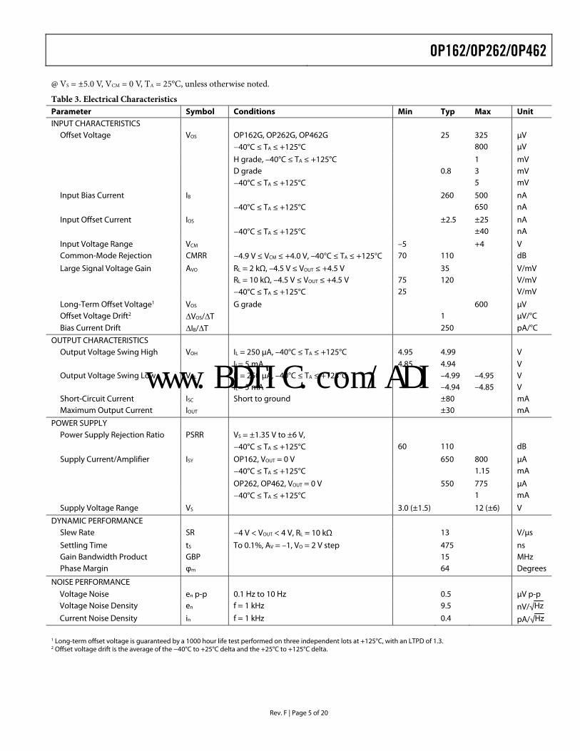
@ VS = ±5.0 V, VCM = 0 V, TA = 25°C, unless otherwise noted.
Table 3. Electrical Characteristics Parameter Symbol Conditions Min Typ Max Unit INPUT CHARACTERISTICS
Offset Voltage VOS OP162G, OP262G, OP462G 25 325 µV −40°C ≤ TA ≤ +125°C 800 µV
H grade, –40°C ≤ TA ≤ +125°C 1 mV D grade 0.8 3 mV −40°C ≤ TA ≤ +125°C 5 mV
Input Bias Current IB 260 500 nA −40°C ≤ TA ≤ +125°C 650 nA
Input Offset Current IOS ±2.5 ±25 nA −40°C ≤ TA ≤ +125°C ±40 nA
Input Voltage Range VCM –5 +4 V Common-Mode Rejection CMRR −4.9 V ≤ VCM ≤ +4.0 V, –40°C ≤ TA ≤ +125°C 70 110 dB
Large Signal Voltage Gain AVO RL = 2 kΩ, –4.5 V ≤ VOUT ≤ +4.5 V 35 V/mV RL = 10 kΩ, –4.5 V ≤ VOUT ≤ +4.5 V 75 120 V/mV −40°C ≤ TA ≤ +125°C 25 V/mV
Long-Term Offset Voltage1 VOS G grade 600 µV Offset Voltage Drift2 ∆VOS/∆T 1 µV/°C Bias Current Drift ∆IB/∆T 250 pA/°C
OUTPUT CHARACTERISTICS Output Voltage Swing High VOH IL = 250 µA, –40°C ≤ TA ≤ +125°C 4.95 4.99 V IL= 5 mA 4.85 4.94 V Output Voltage Swing Low VOL IL = 250 µA, –40°C ≤ TA ≤ +125°C –4.99 –4.95 V IL= 5 mA –4.94 –4.85 V Short-Circuit Current ISC Short to ground ±80 mA Maximum Output Current IOUT ±30 mA
POWER SUPPLY Power Supply Rejection Ratio PSRR VS = ±1.35 V to ±6 V, −40°C ≤ TA ≤ +125°C 60 110 dB
Supply Current/Amplifier ISY OP162, VOUT = 0 V 650 800 µA −40°C ≤ TA ≤ +125°C 1.15 mA
OP262, OP462, VOUT = 0 V 550 775 µA −40°C ≤ TA ≤ +125°C 1 mA
Supply Voltage Range VS 3.0 (±1.5) 12 (±6) V
DYNAMIC PERFORMANCE Slew Rate SR −4 V < VOUT < 4 V, RL = 10 kΩ 13 V/µs
Settling Time tS To 0.1%, AV = –1, VO = 2 V step 475 ns Gain Bandwidth Product GBP 15 MHz Phase Margin φm 64 Degrees
NOISE PERFORMANCE Voltage Noise en p-p 0.1 Hz to 10 Hz 0.5 µV p-p Voltage Noise Density en f = 1 kHz 9.5 nV/√Hz Current Noise Density in f = 1 kHz 0.4 pA/√Hz
1 Long-term offset voltage is guaranteed by a 1000 hour life test performed on three independent lots at +125°C, with an LTPD of 1.3. 2 Offset voltage drift is the average of the −40°C to +25°C delta and the +25°C to +125°C delta.
www.BDTIC.com/ADI
OP162/OP262/OP462
Rev. F | Page 6 of 20
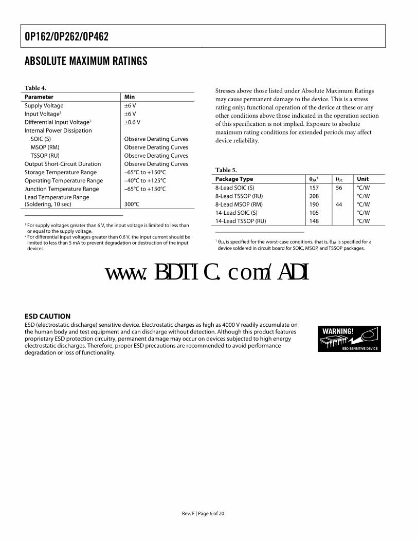
ABSOLUTE MAXIMUM RATINGS
Table 4. Parameter Min Supply Voltage ±6 V Input Voltage1 ±6 V Differential Input Voltage2 ±0.6 V Internal Power Dissipation
SOIC (S) Observe Derating Curves MSOP (RM) Observe Derating Curves TSSOP (RU) Observe Derating Curves
Output Short-Circuit Duration Observe Derating Curves Storage Temperature Range –65°C to +150°C Operating Temperature Range –40°C to +125°C Junction Temperature Range –65°C to +150°C Lead Temperature Range (Soldering, 10 sec) 300°C
1 For supply voltages greater than 6 V, the input voltage is limited to less than
or equal to the supply voltage. 2 For differential input voltages greater than 0.6 V, the input current should be
limited to less than 5 mA to prevent degradation or destruction of the input devices.
Stresses above those listed under Absolute Maximum Ratings may cause permanent damage to the device. This is a stress rating only; functional operation of the device at these or any other conditions above those indicated in the operation section of this specification is not implied. Exposure to absolute maximum rating conditions for extended periods may affect device reliability.
Table 5. Package Type θJA
1 θJC Unit
8-Lead SOIC (S) 157 56 °C/W 8-Lead TSSOP (RU) 208 °C/W 8-Lead MSOP (RM) 190 44 °C/W 14-Lead SOIC (S) 105 °C/W 14-Lead TSSOP (RU) 148 °C/W ____________________________ 1 θJA is specified for the worst-case conditions, that is, θJA is specified for a
device soldered in circuit board for SOIC, MSOP, and TSSOP packages.
ESD CAUTION ESD (electrostatic discharge) sensitive device. Electrostatic charges as high as 4000 V readily accumulate on the human body and test equipment and can discharge without detection. Although this product features proprietary ESD protection circuitry, permanent damage may occur on devices subjected to high energy electrostatic discharges. Therefore, proper ESD precautions are recommended to avoid performance degradation or loss of functionality.
www.BDTIC.com/ADI
OP162/OP262/OP462
Rev. F | Page 7 of 20
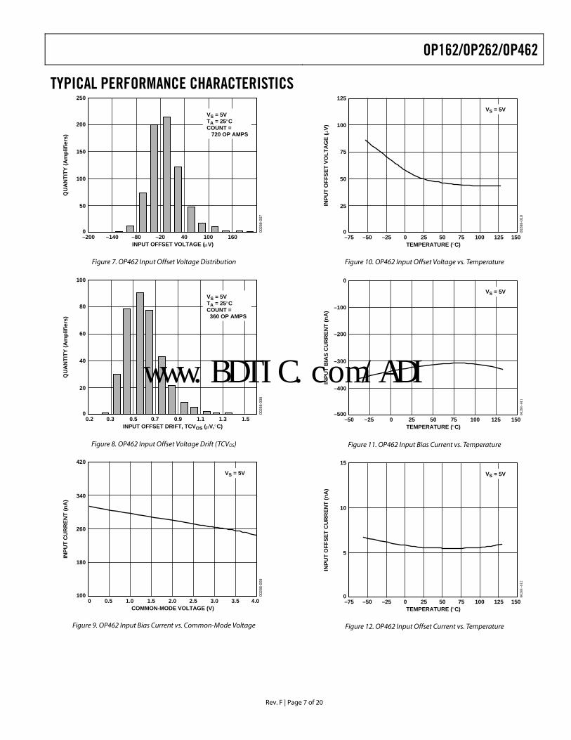
TYPICAL PERFORMANCE CHARACTERISTICS
VS = 5VTA = 25°CCOUNT = 720 OP AMPS
INPUT OFFSET VOLTAGE (µV)
QU
AN
TITY
(Am
plifi
ers)
250
200
150
50
100
0–200 –140 –80 –20 10040 160
0028
8-00
7
Figure 7. OP462 Input Offset Voltage Distribution
VS = 5VTA = 25°CCOUNT = 360 OP AMPS
INPUT OFFSET DRIFT, TCVOS (µV,°C)
QU
AN
TITY
(Am
plifi
ers)
100
80
60
20
40
00.2 0.3 0.5 0.7 0.9 1.31.1 1.5
0028
8-00
8
Figure 8. OP462 Input Offset Voltage Drift (TCVOS)
COMMON-MODE VOLTAGE (V)
INPU
T C
UR
REN
T (n
A)
420
340
260
180
1000 0.5 1.0 1.5 2.0 3.02.5 3.5 4.0
0028
8-00
9
VS = 5V
Figure 9. OP462 Input Bias Current vs. Common-Mode Voltage
TEMPERATURE (°C)
INPU
T O
FFSE
T VO
LTA
GE
(µV)
125
100
75
50
25
0–75 –50 –25 0 25 50 10075 125 150
0028
8-01
0
VS = 5V
Figure 10. OP462 Input Offset Voltage vs. Temperature
TEMPERATURE (°C)
INPU
T B
IAS
CU
RR
ENT
(nA
)
0
–100
–200
–300
–400
–500–50 –25 0 25 50 10075 125 150
00288−011
VS = 5V
Figure 11. OP462 Input Bias Current vs. Temperature
TEMPERATURE (°C)
INPU
T O
FFSE
T C
UR
REN
T (n
A)
15
10
5
0–75 –50 –25 0 25 50 10075 125 150
00288−012
VS = 5V
Figure 12. OP462 Input Offset Current vs. Temperature
www.BDTIC.com/ADI
OP162/OP262/OP462
Rev. F | Page 8 of 20
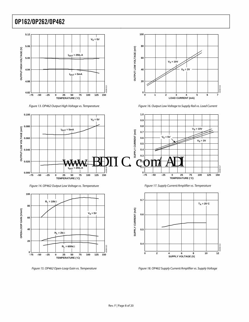
TEMPERATURE (°C)
OU
TPU
T H
IGH
VO
LTA
GE
(V)
5.12
5.06
5.00
4.94
4.88
4.82–75 –50 –25 0 25 50 10075 125 150
0028
8-01
3
VS = 5V
IOUT = 250µA
IOUT = 5mA
Figure 13. OP462 Output High Voltage vs. Temperature
TEMPERATURE (°C)
OU
TPU
T LO
W V
OLT
AG
E (m
V)
0.100
0.080
0.060
0.040
0.020
0.000–75 –50 –25 0 25 50 10075 125 150
0028
8-01
4
VS = 5V
IOUT = 250µA
IOUT = 5mA
Figure 14. OP462 Output Low Voltage vs. Temperature
TEMPERATURE (°C)
OPE
N-L
OO
P G
AIN
(V/m
V)
100
80
60
40
20
0–75 –50 –25 0 25 50 10075 125 150
0028
8-01
5
VS = 5V
RL = 10kΩ
RL = 2kΩ
RL = 600kΩ
Figure 15. OP462 Open-Loop Gain vs. Temperature
LOAD CURRENT (mA)
OU
TPU
T LO
W V
OLT
AG
E (m
V)
100
80
60
40
20
00 1 2 3 4 5 6 7
0028
8-01
6
VS = 3V
VS = 10V
Figure 16. Output Low Voltage to Supply Rail vs. Load Current
TEMPERATURE (°C)
SUPP
LY C
UR
REN
T (m
A)
1.0
0.9
0.8
0.7
0.6
0.5
0.4
0.3
0.2
0.1
0–75 –50 –25 0 25 10075 125 150
0028
8-01
7
VS = 5V
VS = 10V
VS = 3V
Figure 17. Supply Current/Amplifier vs. Temperature
SUPPLY VOLTAGE (V)
SUPP
LY C
UR
REN
T (m
A)
0.7
0.6
0.5
0.4
0 2 4 6 8 10 1
0028
8-01
8
2
TA = 25°C
Figure 18. OP462 Supply Current/Amplifier vs. Supply Voltage
www.BDTIC.com/ADI
OP162/OP262/OP462
Rev. F | Page 9 of 20
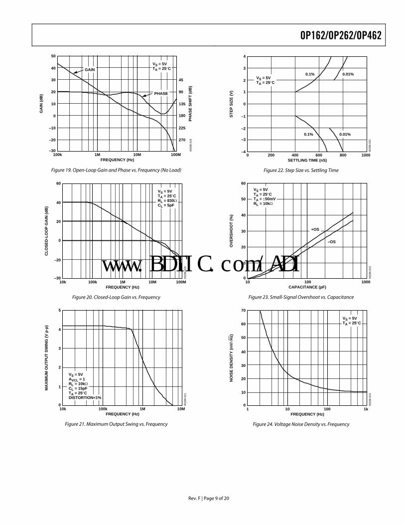
FREQUENCY (Hz)
GA
IN (d
B)
50
40
30
20
10
0
–10
–20
–30
PHA
SE S
HIF
T (d
B)
45
90
135
180
225
270
100k 1M 10M 100M
0028
8-01
9
VS = 5VTA = 25°CGAIN
PHASE
Figure 19. Open-Loop Gain and Phase vs. Frequency (No Load)
FREQUENCY (Hz)
CLO
SED
-LO
OP
GA
IN (d
B)
60
40
20
0
–20
–3010k 100k 1M 10M 100M
0028
8-02
0
VS = 5VTA = 25°CRL = 830ΩCL = 5pF
Figure 20. Closed-Loop Gain vs. Frequency
FREQUENCY (Hz)
MA
XIM
UM
OU
TPU
T SW
ING
(V p
-p)
5
4
3
2
1
010k 100k 1M 10M
0028
8-02
1
VS = 5VAVCL = 1RL = 10kΩCL = 15pFTA = 25°CDISTORTION<1%
Figure 21. Maximum Output Swing vs. Frequency
SETTLING TIME (nS)
STEP
SIZ
E (V
)
3
1
–1
–3
2
4
0
–2
–40 200 400 600 800 1000
0028
8-02
2
0.01%0.1%
0.01%0.1%
VS = 5VTA = 25°C
Figure 22. Step Size vs. Settling Time
CAPACITANCE (pF)
OVE
RSH
OO
T (%
)
60
40
50
30
20
10
010 100 1000
0028
8-02
3
VS = 5VTA = 25°CTA = ±50mVRL = 10kΩ
+OS
–OS
Figure 23. Small-Signal Overshoot vs. Capacitance
FREQUENCY (Hz)
NO
ISE
DEN
SITY
(nV/√H
z)
70
60
50
40
30
10
20
01 10 100 1k
0028
8-02
4
VS = 5VTA = 25°C
Figure 24. Voltage Noise Density vs. Frequency
www.BDTIC.com/ADI
OP162/OP262/OP462
Rev. F | Page 10 of 20
FREQUENCY (Hz)
NO
ISE
DEN
SITY
(pA
/√H
z)
7
6
5
4
3
1
2
01 10 100 1k
0028
8-02
5
VS = 5VTA = 25°C
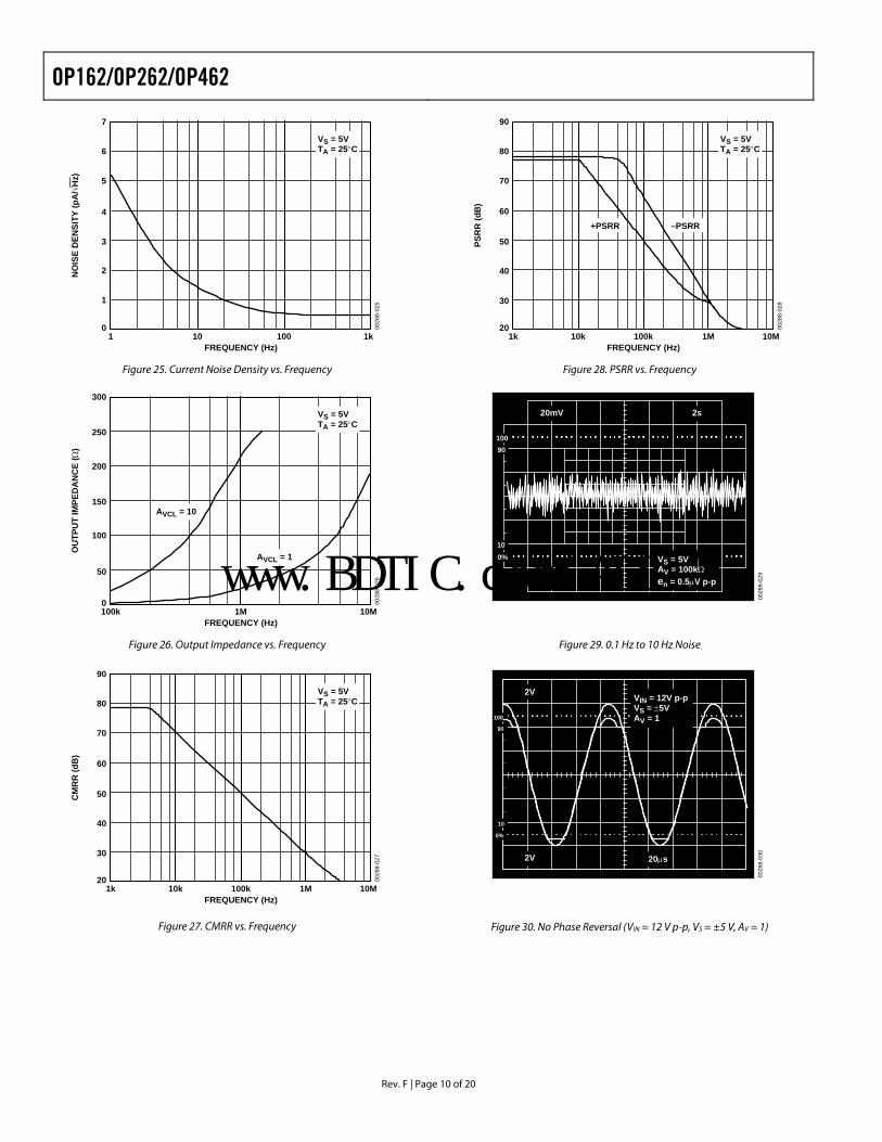
Figure 25. Current Noise Density vs. Frequency
FREQUENCY (Hz)
OU
TPU
T IM
PED
AN
CE
(Ω)
300
250
200
150
50
100
0100k 1M 10M
0028
8-02
6
VS = 5VTA = 25°C
AVCL = 10
AVCL = 1
Figure 26. Output Impedance vs. Frequency
FREQUENCY (Hz)
CM
RR
(dB
)
90
80
70
60
50
30
40
201k 10k 100k 1M 10M
0028
8-02
7
VS = 5VTA = 25°C
Figure 27. CMRR vs. Frequency
FREQUENCY (Hz)
PSR
R (d
B)
90
80
70
60
50
30
40
201k 10k 100k 1M 10M
0028
8-02
8
VS = 5VTA = 25°C
+PSRR –PSRR
Figure 28. PSRR vs. Frequency
0028
8-02
9
10090
100%
VS = 5VAV = 100kΩen = 0.5µV p-p
2s20mV
Figure 29. 0.1 Hz to 10 Hz Noise
10
0%
100
90
0028
8-03
0
VIN = 12V p-pVS = ±5VAV = 1
2V
2V
20µs
Figure 30. No Phase Reversal (VIN = 12 V p-p, VS = ±5 V, AV = 1)
www.BDTIC.com/ADI
OP162/OP262/OP462
Rev. F | Page 11 of 20
0028
8-03
1
100%
10090
200ns20mV
VS = 5VAV = 1TA = 25°CCL = 100pF
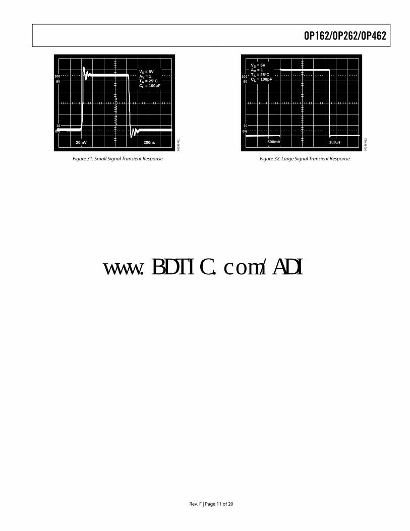
Figure 31. Small Signal Transient Response
0028
8-03
2
100%
10090
100µs500mV
VS = 5VAV = 1TA = 25°CCL = 100pF
Figure 32. Large Signal Transient Response
www.BDTIC.com/ADI
OP162/OP262/OP462
Rev. F | Page 12 of 20
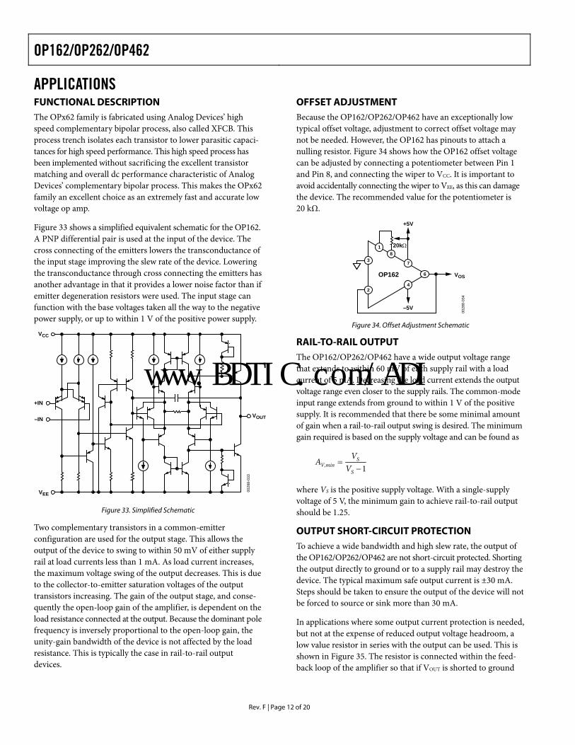
APPLICATIONS FUNCTIONAL DESCRIPTION The OPx62 family is fabricated using Analog Devices’ high speed complementary bipolar process, also called XFCB. This process trench isolates each transistor to lower parasitic capaci-tances for high speed performance. This high speed process has been implemented without sacrificing the excellent transistor matching and overall dc performance characteristic of Analog Devices’ complementary bipolar process. This makes the OPx62 family an excellent choice as an extremely fast and accurate low voltage op amp.
Figure 33 shows a simplified equivalent schematic for the OP162. A PNP differential pair is used at the input of the device. The cross connecting of the emitters lowers the transconductance of the input stage improving the slew rate of the device. Lowering the transconductance through cross connecting the emitters has another advantage in that it provides a lower noise factor than if emitter degeneration resistors were used. The input stage can function with the base voltages taken all the way to the negative power supply, or up to within 1 V of the positive power supply.
VCC
VEE
+IN
–IN VOUT
0028
8-03
3
Figure 33. Simplified Schematic
Two complementary transistors in a common-emitter configuration are used for the output stage. This allows the output of the device to swing to within 50 mV of either supply rail at load currents less than 1 mA. As load current increases, the maximum voltage swing of the output decreases. This is due to the collector-to-emitter saturation voltages of the output transistors increasing. The gain of the output stage, and conse-quently the open-loop gain of the amplifier, is dependent on the load resistance connected at the output. Because the dominant pole frequency is inversely proportional to the open-loop gain, the unity-gain bandwidth of the device is not affected by the load resistance. This is typically the case in rail-to-rail output devices.
OFFSET ADJUSTMENT Because the OP162/OP262/OP462 have an exceptionally low typical offset voltage, adjustment to correct offset voltage may not be needed. However, the OP162 has pinouts to attach a nulling resistor. Figure 34 shows how the OP162 offset voltage can be adjusted by connecting a potentiometer between Pin 1 and Pin 8, and connecting the wiper to VCC. It is important to avoid accidentally connecting the wiper to VEE, as this can damage the device. The recommended value for the potentiometer is 20 kΩ.
–5V
20kΩ
OP162
+5V
VOS
3
24
7
81
6
0028
8-03
4
Figure 34. Offset Adjustment Schematic
RAIL-TO-RAIL OUTPUT The OP162/OP262/OP462 have a wide output voltage range that extends to within 60 mV of each supply rail with a load current of 5 mA. Decreasing the load current extends the output voltage range even closer to the supply rails. The common-mode input range extends from ground to within 1 V of the positive supply. It is recommended that there be some minimal amount of gain when a rail-to-rail output swing is desired. The minimum gain required is based on the supply voltage and can be found as
1−=
S
SV,min V
VA
where VS is the positive supply voltage. With a single-supply voltage of 5 V, the minimum gain to achieve rail-to-rail output should be 1.25.
OUTPUT SHORT-CIRCUIT PROTECTION To achieve a wide bandwidth and high slew rate, the output of the OP162/OP262/OP462 are not short-circuit protected. Shorting the output directly to ground or to a supply rail may destroy the device. The typical maximum safe output current is ±30 mA. Steps should be taken to ensure the output of the device will not be forced to source or sink more than 30 mA.
In applications where some output current protection is needed, but not at the expense of reduced output voltage headroom, a low value resistor in series with the output can be used. This is shown in Figure 35. The resistor is connected within the feed-back loop of the amplifier so that if VOUT is shorted to ground
www.BDTIC.com/ADI
OP162/OP262/OP462
Rev. F | Page 13 of 20
and VIN swings up to 5 V, the output current will not exceed 30 mA. For single 5 V supply applications, resistors less than 169 Ω are not recommended.
OPx62VIN
VOUT169Ω
5V
0028
8-03
5
Figure 35. Output Short-Circuit Protection
INPUT OVERVOLTAGE PROTECTION The input voltage should be limited to ±6 V, or damage to the device can occur. Electrostatic protection diodes placed in the input stage of the device help protect the amplifier from static discharge. Diodes are connected between each input as well as from each input to both supply pins as shown in the simplified equivalent circuit in Figure 33. If an input voltage exceeds either supply voltage by more than 0.6 V, or if the differential input voltage is greater than 0.6 V, these diodes energize causing overvoltage damage.
The input current should be limited to less than 5 mA to prevent degradation or destruction of the device by placing an external resistor in series with the input at risk of being overdriven. The size of the resistor can be calculated by dividing the maxi-mum input voltage by 5 mA. For example, if the differential input voltage could reach 5 V, the external resistor should be 5 V/5 mA = 1 kΩ. In practice, this resistor should be placed in series with both inputs to balance any offset voltages created by the input bias current.
OUTPUT PHASE REVERSAL The OP162/OP262/OP462 are immune to phase reversal as long as the input voltage is limited to ±6 V. Figure 30 shows the output of a device with the input voltage driven beyond the supply voltages. Although the device’s output does not change phase, large currents due to input overvoltage could result, damaging the device. In applications where the possibility of an input voltage exceeding the supply voltage exists, overvoltage protection should be used, as described in the previous section.
POWER DISSIPATION The maximum power that can be safely dissipated by the OP162/OP262/OP462 is limited by the associated rise in junction temperature. The maximum safe junction temperature is 150°C; device performance suffers when this limit is exceeded. If this maximum is only momentarily exceeded, proper circuit operation will be restored as soon as the die temperature is reduced. Leaving the device in an “overheated” condition for an extended period can result in permanent damage to the device.
To calculate the internal junction temperature of the OPx62, use the formula
TJ = PDISS × θJA + TA
where: TJ is the OPx62 junction temperature. PDISS is the OPx62 power dissipation. θJA is the OPx62 package thermal resistance, junction-to-ambient temperature. TA is the ambient temperature of the circuit.
The power dissipated by the device can be calculated as
PDISS = ILOAD × (VS – VOUT)
where: ILOAD is the OPx62 output load current. VS is the OPx62 supply voltage. VOUT is the OPx62 output voltage.
Figure 36 and Figure 37 provide a convenient way to determine if the device is being overheated. The maximum safe power dissipation can be found graphically, based on the package type and the ambient temperature around the package. By using the previous equation, it is a simple matter to see if PDISS exceeds the device’s power derating curve. To ensure proper operation, it is important to observe the recommended derating curves shown in Figure 36 and Figure 37.
AMBIENT TEMPERATURE (°C)
MA
XIM
UM
PO
WER
DIS
SIPA
TIO
N (W
atts
)
0.9
0.7
0.8
0.5
0.6
0.1
0.2
0.3
0.4
020 40 60 10080 120
0028
8-03
6
8-LEAD SOIC
8-LEAD MSOP
8-LEAD TSSOP
Figure 36. Maximum Power Dissipation vs. Temperature for 8-Lead Package Types
www.BDTIC.com/ADI
OP162/OP262/OP462
Rev. F | Page 14 of 20
AMBIENT TEMPERATURE (°C)
MA
XIM
UM
PO
WER
DIS
SIPA
TIO
N (W
atts
)
0.3
0.4
0.5
0.6
0.7
0.8
0.9
1.0
1.1
1.2
0.1
0.2
020 45 70 95 120
0028
8-03
7
14-LEAD SOIC
14-LEAD TSSOP
Figure 37. Maximum Power Dissipation vs. Temperature for 14-Lead Package Types
UNUSED AMPLIFIERS It is recommended that any unused amplifiers in a dual or a quad package be configured as a unity-gain follower with a 1 kΩ feedback resistor connected from the inverting input to the output, and the noninverting input tied to the ground plane.
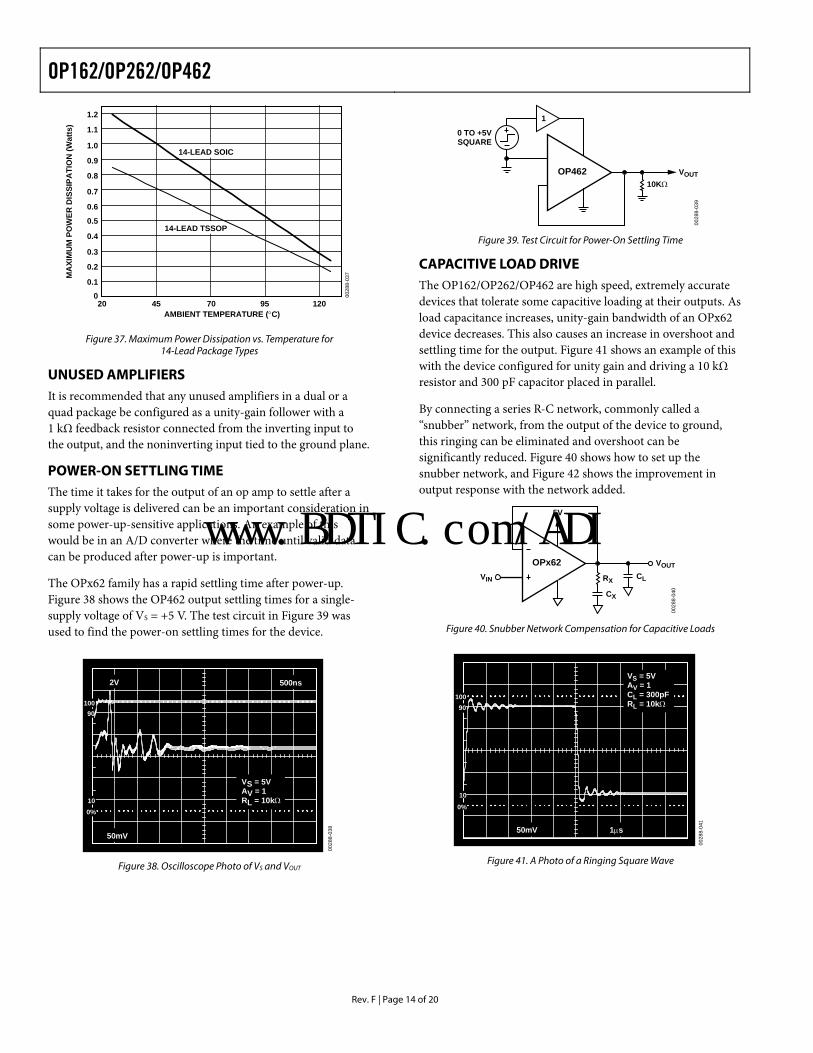
POWER-ON SETTLING TIME The time it takes for the output of an op amp to settle after a supply voltage is delivered can be an important consideration in some power-up-sensitive applications. An example of this would be in an A/D converter where the time until valid data can be produced after power-up is important.
The OPx62 family has a rapid settling time after power-up. Figure 38 shows the OP462 output settling times for a single-supply voltage of VS = +5 V. The test circuit in Figure 39 was used to find the power-on settling times for the device.
100%
10090
500ns2V
50mV
VS = 5VAV = 1RL = 10kΩ
0028
8-03
8
Figure 38. Oscilloscope Photo of VS and VOUT
OP462 VOUT
0 TO +5VSQUARE
10KΩ
0028
8-03
9
1
Figure 39. Test Circuit for Power-On Settling Time
CAPACITIVE LOAD DRIVE The OP162/OP262/OP462 are high speed, extremely accurate devices that tolerate some capacitive loading at their outputs. As load capacitance increases, unity-gain bandwidth of an OPx62 device decreases. This also causes an increase in overshoot and settling time for the output. Figure 41 shows an example of this with the device configured for unity gain and driving a 10 kΩ resistor and 300 pF capacitor placed in parallel.
By connecting a series R-C network, commonly called a “snubber” network, from the output of the device to ground, this ringing can be eliminated and overshoot can be significantly reduced. Figure 40 shows how to set up the snubber network, and Figure 42 shows the improvement in output response with the network added.
OPx62VIN
VOUT
RX
CX
CL
5V
0028
8-04
0
Figure 40. Snubber Network Compensation for Capacitive Loads
0028
8-04
1
50mV 1µs
10090
10
0%
VS = 5VAV = 1CL = 300pFRL = 10kΩ
Figure 41. A Photo of a Ringing Square Wave
www.BDTIC.com/ADI
OP162/OP262/OP462
Rev. F | Page 15 of 20
0028
8-04
2
100%
10090
50mV 1µs
VS = 5VAV = 1CL = 300pFRL = 10kΩ
WITH SNUBBER: RX = 140Ω CX = 10nF
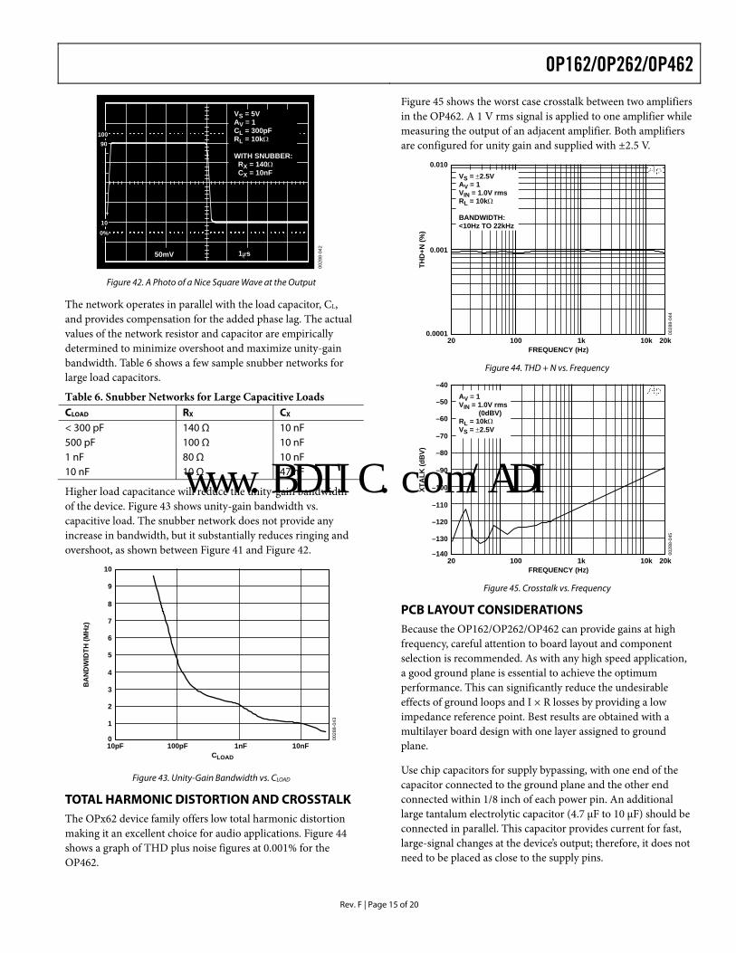
Figure 45 shows the worst case crosstalk between two amplifiers in the OP462. A 1 V rms signal is applied to one amplifier while measuring the output of an adjacent amplifier. Both amplifiers are configured for unity gain and supplied with ±2.5 V.
FREQUENCY (Hz)
THD
+N (%
)
0.010
0.001
0.000120 100 1k 10k 20k
0028
8-04
4
VS = ±2.5VAV = 1VIN = 1.0V rmsRL = 10kΩ
BANDWIDTH:<10Hz TO 22kHz
Figure 42. A Photo of a Nice Square Wave at the Output
The network operates in parallel with the load capacitor, CL, and provides compensation for the added phase lag. The actual values of the network resistor and capacitor are empirically determined to minimize overshoot and maximize unity-gain bandwidth. Table 6 shows a few sample snubber networks for large load capacitors.
Figure 44. THD + N vs. Frequency
FREQUENCY (Hz)
XTA
LK (d
BV)
–40
–90
–80
–70
–60
–50
–140
–130
–120
–110
–100
20 100 1k 10k 20k
0028
8-04
5
AV = 1VIN = 1.0V rms (0dBV)RL = 10kΩVS = ±2.5V
Table 6. Snubber Networks for Large Capacitive Loads CLOAD RX CX < 300 pF 140 Ω 10 nF 500 pF 100 Ω 10 nF 1 nF 80 Ω 10 nF 10 nF 10 Ω 47 nF
Higher load capacitance will reduce the unity-gain bandwidth of the device. Figure 43 shows unity-gain bandwidth vs. capacitive load. The snubber network does not provide any increase in bandwidth, but it substantially reduces ringing and overshoot, as shown between Figure 41 and Figure 42.
CLOAD
BA
ND
WID
TH (M
Hz)
10
7
8
9
5
6
4
3
2
1
010pF 100pF 1nF 10nF
0028
8-04
3
Figure 45. Crosstalk vs. Frequency
PCB LAYOUT CONSIDERATIONS Because the OP162/OP262/OP462 can provide gains at high frequency, careful attention to board layout and component selection is recommended. As with any high speed application, a good ground plane is essential to achieve the optimum performance. This can significantly reduce the undesirable effects of ground loops and I × R losses by providing a low impedance reference point. Best results are obtained with a multilayer board design with one layer assigned to ground plane.
Use chip capacitors for supply bypassing, with one end of the capacitor connected to the ground plane and the other end connected within 1/8 inch of each power pin. An additional large tantalum electrolytic capacitor (4.7 µF to 10 µF) should be connected in parallel. This capacitor provides current for fast, large-signal changes at the device’s output; therefore, it does not need to be placed as close to the supply pins.
Figure 43. Unity-Gain Bandwidth vs. CLOAD
TOTAL HARMONIC DISTORTION AND CROSSTALK The OPx62 device family offers low total harmonic distortion making it an excellent choice for audio applications. Figure 44 shows a graph of THD plus noise figures at 0.001% for the OP462.
www.BDTIC.com/ADI
OP162/OP262/OP462
Rev. F | Page 16 of 20
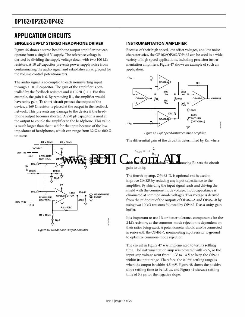
APPLICATION CIRCUITS SINGLE-SUPPLY STEREO HEADPHONE DRIVER Figure 46 shows a stereo headphone output amplifier that can operate from a single 5 V supply. The reference voltage is derived by dividing the supply voltage down with two 100 kΩ resistors. A 10 µF capacitor prevents power supply noise from contaminating the audio signal and establishes an ac ground for the volume control potentiometers.
The audio signal is ac-coupled to each noninverting input through a 10 µF capacitor. The gain of the amplifier is con-trolled by the feedback resistors and is (R2/R1) + 1. For this example, the gain is 6. By removing R1, the amplifier would have unity gain. To short-circuit protect the output of the device, a 169 Ω resistor is placed at the output in the feedback network. This prevents any damage to the device if the head-phone output becomes shorted. A 270 µF capacitor is used at the output to couple the amplifier to the headphone. This value is much larger than that used for the input because of the low impedance of headphones, which can range from 32 Ω to 600 Ω or more.
OP262-A
5V
169Ω 270µF
47kΩ
L VOLUMECONTROL
R1 = 10kΩ
10µF
10µF
10kΩ5V
100kΩ
10µF
100kΩ
R2 = 50kΩ
LEFT IN
OP262-B
5V
169Ω 270µF
47kΩ
HEADPHONERIGHT
HEADPHONELEFT
10kΩ
R VOLUMECONTROL
10µFRIGHT IN
R2 = 50kΩ
10µF
R1 = 10kΩ
0028
8-04
6
Figure 46. Headphone Output Amplifier
INSTRUMENTATION AMPLIFIER Because of their high speed, low offset voltages, and low noise characteristics, the OP162/OP262/OP462 can be used in a wide variety of high speed applications, including precision instru-mentation amplifiers. Figure 47 shows an example of such an application.
OP462-A
OP462-B
OP462-COP462-D
–VIN
+VIN
1kΩ
10kΩ
2kΩ
1.9kΩ
200Ω10 TURN(OPTIONAL)
OUTPUTRG 1kΩ
10kΩ
2kΩ
2kΩ
0028
8-04
7
Figure 47. High Speed Instrumentation Amplifier
The differential gain of the circuit is determined by RG, where
GDIFF R
A 21+=
with the RG resistor value in kΩ. Removing RG sets the circuit gain to unity.
The fourth op amp, OP462-D, is optional and is used to improve CMRR by reducing any input capacitance to the amplifier. By shielding the input signal leads and driving the shield with the common-mode voltage, input capacitance is eliminated at common-mode voltages. This voltage is derived from the midpoint of the outputs of OP462-A and OP462-B by using two 10 kΩ resistors followed by OP462-D as a unity-gain buffer.
It is important to use 1% or better tolerance components for the 2 kΩ resistors, as the common-mode rejection is dependent on their ratios being exact. A potentiometer should also be connected in series with the OP462-C noninverting input resistor to ground to optimize common-mode rejection.
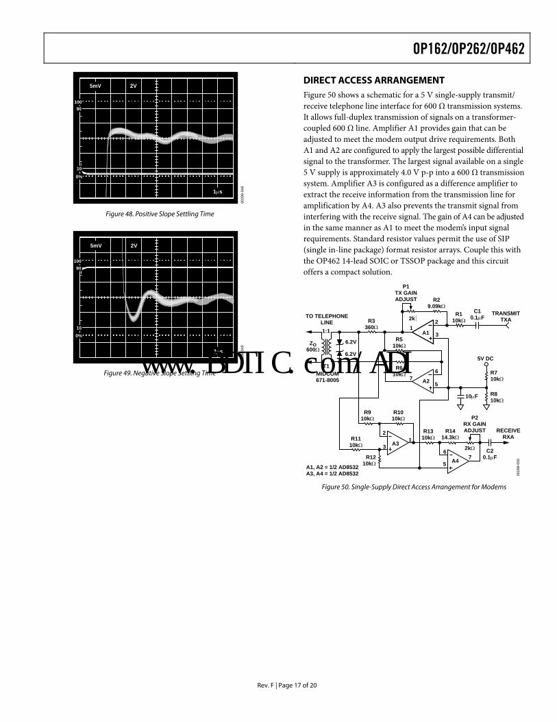
The circuit in Figure 47 was implemented to test its settling time. The instrumentation amp was powered with −5 V, so the input step voltage went from −5 V to +4 V to keep the OP462 within its input range. Therefore, the 0.05% settling range is when the output is within 4.5 mV. Figure 48 shows the positive slope settling time to be 1.8 µs, and Figure 49 shows a settling time of 3.9 µs for the negative slope.
www.BDTIC.com/ADI
OP162/OP262/OP462
Rev. F | Page 17 of 20
0028
8-04
8
10
0%
10090
1µs
5mV 2V
Figure 48. Positive Slope Settling Time
0028
8-04
9
100%
10090
5mV
1µs
100%
10090
1µs
5mV 2V
Figure 49. Negative Slope Settling Time
DIRECT ACCESS ARRANGEMENT Figure 50 shows a schematic for a 5 V single-supply transmit/ receive telephone line interface for 600 Ω transmission systems. It allows full-duplex transmission of signals on a transformer-coupled 600 Ω line. Amplifier A1 provides gain that can be adjusted to meet the modem output drive requirements. Both A1 and A2 are configured to apply the largest possible differential signal to the transformer. The largest signal available on a single 5 V supply is approximately 4.0 V p-p into a 600 Ω transmission system. Amplifier A3 is configured as a difference amplifier to extract the receive information from the transmission line for amplification by A4. A3 also prevents the transmit signal from interfering with the receive signal. The gain of A4 can be adjusted in the same manner as A1 to meet the modem’s input signal requirements. Standard resistor values permit the use of SIP (single in-line package) format resistor arrays. Couple this with the OP462 14-lead SOIC or TSSOP package and this circuit offers a compact solution.
6.2V
6.2V
TRANSMITTXA
RECEIVERXA
2k
P1TX GAINADJUST
A1
A2
A3
A4A1, A2 = 1/2 AD8532A3, A4 = 1/2 AD8532
R3360Ω
ZO600Ω
R110kΩ
R1310kΩ
R1010kΩ
R910kΩ
R1110kΩ
C20.1µF
C10.1µF
10µF
R1210kΩ
R710kΩ
R810kΩ
R510kΩ
R610kΩ
R1414.3kΩ
R29.09kΩ
1:1
T1
TO TELEPHONELINE
12
3
76
5
2
31
6
57
P2RX GAINADJUST
2kΩ
5V DC
MIDCOM671-8005
0028
8-05
0
Figure 50. Single-Supply Direct Access Arrangement for Modems
www.BDTIC.com/ADI
OP162/OP262/OP462
Rev. F | Page 18 of 20
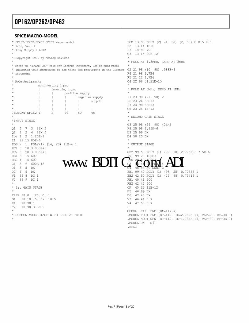
SPICE MACRO-MODEL * OP162/OP262/OP462 SPICE Macro-model * 7/96, Ver. 1 * Troy Murphy / ADSC * * Copyright 1996 by Analog Devices * * Refer to “README.DOC” file for License Statement. Use of this model * indicates your acceptance of the terms and provisions in the License * Statement * * Node Assignments * noninverting input * | inverting input * | | positive supply * | | | negative supply * | | | | output * | | | | | * | | | | | .SUBCKT OP162 1 2 99 50 45 * *INPUT STAGE * Q1 5 7 3 PIX 5 Q2 6 2 4 PIX 5 Ios 1 2 1.25E-9 I1 99 15 85E-6 EOS 7 1 POLY(1) (14, 20) 45E-6 1 RC1 5 50 3.035E+3 RC2 6 50 3.035E+3 RE1 3 15 607 RE2 4 15 607 C1 5 6 600E-15 D1 3 8 DX D2 4 9 DX V1 99 8 DC 1 V2 99 9 DC 1 * * 1st GAIN STAGE * EREF 98 0 (20, 0) 1 G1 98 10 (5, 6) 10.5 R1 10 98 1 C2 10 98 3.3E-9 * * COMMON-MODE STAGE WITH ZERO AT 4kHz *
ECM 13 98 POLY (2) (1, 98) (2, 98) 0 0.5 0.5 R2 13 14 1E+6 R3 14 98 70 C3 13 14 80E-12 * * POLE AT 1.5MHz, ZERO AT 3MHz * G2 21 98 (10, 98) .588E-6 R4 21 98 1.7E6 R5 21 22 1.7E6 C4 22 98 31.21E-15 * * POLE AT 6MHz, ZERO AT 3MHz * E1 23 98 (21, 98) 2 R6 23 24 53E+3 R7 24 98 53E+3 C5 23 24 1E-12 * * SECOND GAIN STAGE * G3 25 98 (24, 98) 40E-6 R8 25 98 1.65E+6 D3 25 99 DX D4 50 25 DX * * OUTPUT STAGE * GSY 99 50 POLY (1) (99, 50) 277.5E-6 7.5E-6 R9 99 20 100E3 R10 20 50 100E3 Q3 45 41 99 POUT 4 Q4 45 43 50 NOUT 2 EB1 99 40 POLY (1) (98, 25) 0.70366 1 EB2 42 50 POLY (1) (25, 98) 0.73419 1 RB1 40 41 500 RB2 42 43 500 CF 45 25 11E-12 D5 46 99 DX D6 47 43 DX V3 46 41 0.7 V4 47 50 0.7 . MODEL PIX PNP (Bf=117.7) .MODEL POUT PNP (BF=119, IS=2.782E-17, VAF=28, KF=3E-7) .MODEL NOUT NPN (BF=110, IS=1.786E-17, VAF=90, KF=3E-7) .MODEL DX D() .ENDS
www.BDTIC.com/ADI
OP162/OP262/OP462
Rev. F | Page 19 of 20
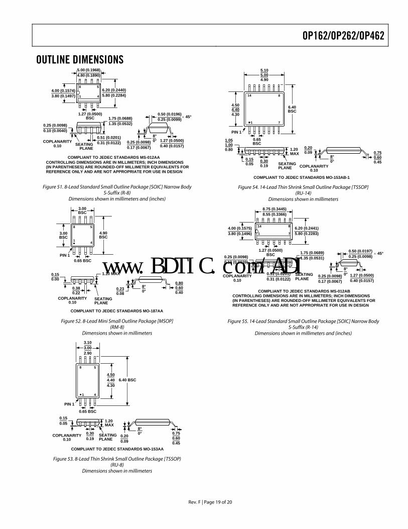
OUTLINE DIMENSIONS
0.25 (0.0098)0.17 (0.0067)
1.27 (0.0500)0.40 (0.0157)
0.50 (0.0196)0.25 (0.0099)× 45°
8°0°
1.75 (0.0688)1.35 (0.0532)
SEATINGPLANE
0.25 (0.0098)0.10 (0.0040)
41
8 5
5.00 (0.1968)4.80 (0.1890)
4.00 (0.1574)3.80 (0.1497)
1.27 (0.0500)BSC
6.20 (0.2440)5.80 (0.2284)
0.51 (0.0201)0.31 (0.0122)COPLANARITY
0.10
CONTROLLING DIMENSIONS ARE IN MILLIMETERS; INCH DIMENSIONS(IN PARENTHESES) ARE ROUNDED-OFF MILLIMETER EQUIVALENTS FORREFERENCE ONLY AND ARE NOT APPROPRIATE FOR USE IN DESIGN
COMPLIANT TO JEDEC STANDARDS MS-012AA
Figure 51. 8-Lead Standard Small Outline Package [SOIC] Narrow Body S-Suffix (R-8)
Dimensions shown in millimeters and (inches)
0.800.600.40
8°0°
4
8
1
5
4.90BSC
PIN 10.65 BSC
3.00BSC
SEATINGPLANE
0.150.00
0.380.22
1.10 MAX
3.00BSC
COPLANARITY0.10
0.230.08
COMPLIANT TO JEDEC STANDARDS MO-187AA
Figure 52. 8-Lead Mini Small Outline Package [MSOP] (RM-8)
Dimensions shown in millimeters
8 5
41
PIN 1
0.65 BSC
SEATINGPLANE
0.150.05
0.300.19
1.20MAX
0.200.09
8°0°
6.40 BSC4.504.404.30
3.103.002.90
COPLANARITY0.10
0.750.600.45
COMPLIANT TO JEDEC STANDARDS MO-153AA
Figure 53. 8-Lead Thin Shrink Small Outline Package [TSSOP) (RU-8)
Dimensions shown in millimeters
4.504.404.30
14 8
71
6.40BSC
PIN 1
5.105.004.90
0.65BSC
SEATINGPLANE
0.150.05
0.300.19
1.20MAX
1.051.000.80 0.20
0.098°0°
0.750.600.45
COPLANARITY0.10
COMPLIANT TO JEDEC STANDARDS MO-153AB-1
Figure 54. 14-Lead Thin Shrink Small Outline Package [TSSOP] (RU-14)
Dimensions shown in millimeters
CONTROLLING DIMENSIONS ARE IN MILLIMETERS; INCH DIMENSIONS(IN PARENTHESES) ARE ROUNDED-OFF MILLIMETER EQUIVALENTS FORREFERENCE ONLY AND ARE NOT APPROPRIATE FOR USE IN DESIGN
COPLANARITY0.10
14 8
716.20 (0.2441)5.80 (0.2283)
4.00 (0.1575)3.80 (0.1496)
8.75 (0.3445)8.55 (0.3366)
1.27 (0.0500)BSC
SEATINGPLANE
0.25 (0.0098)0.10 (0.0039)
0.51 (0.0201)0.31 (0.0122)
1.75 (0.0689)1.35 (0.0531)
8°0°
0.50 (0.0197)0.25 (0.0098)
1.27 (0.0500)0.40 (0.0157)
0.25 (0.0098)0.17 (0.0067)
COMPLIANT TO JEDEC STANDARDS MS-012AB
× 45°
Figure 55. 14-Lead Standard Small Outline Package [SOIC] Narrow Body S-Suffix (R-14)
Dimensions shown in millimeters and (inches)
www.BDTIC.com/ADI
OP162/OP262/OP462
Rev. F | Page 20 of 20
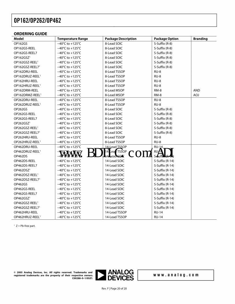
ORDERING GUIDE Model Temperature Range Package Description Package Option Branding OP162GS −40°C to +125°C 8-Lead SOIC S-Suffix (R-8) OP162GS-REEL −40°C to +125°C 8-Lead SOIC S-Suffix (R-8) OP162GS-REEL7 −40°C to +125°C 8-Lead SOIC S-Suffix (R-8) OP162GSZ1 −40°C to +125°C 8-Lead SOIC S-Suffix (R-8) OP162GSZ-REEL1 −40°C to +125°C 8-Lead SOIC S-Suffix (R-8) OP162GSZ-REEL71 −40°C to +125°C 8-Lead SOIC S-Suffix (R-8) OP162DRU-REEL −40°C to +125°C 8-Lead TSSOP RU-8 OP162DRUZ-REEL1 −40°C to +125°C 8-Lead TSSOP RU-8 OP162HRU-REEL −40°C to +125°C 8-Lead TSSOP RU-8 OP162HRUZ-REEL1 −40°C to +125°C 8-Lead TSSOP RU-8 OP162DRM-REEL −40°C to +125°C 8-Lead MSOP RM-8 AND OP162DRMZ-REEL1 −40°C to +125°C 8-Lead MSOP RM-8 AOJ OP262DRU-REEL −40°C to +125°C 8-Lead TSSOP RU-8 OP262DRUZ-REEL1 −40°C to +125°C 8-Lead TSSOP RU-8 OP262GS −40°C to +125°C 8-Lead SOIC S-Suffix (R-8) OP262GS-REEL −40°C to +125°C 8-Lead SOIC S-Suffix (R-8) OP262GS-REEL7 −40°C to +125°C 8-Lead SOIC S-Suffix (R-8) OP262GSZ1 −40°C to +125°C 8-Lead SOIC S-Suffix (R-8) OP262GSZ-REEL1 −40°C to +125°C 8-Lead SOIC S-Suffix (R-8) OP262GSZ-REEL71 −40°C to +125°C 8-Lead SOIC S-Suffix (R-8) OP262HRU-REEL −40°C to +125°C 8-Lead TSSOP RU-8 OP262HRUZ-REEL1 −40°C to +125°C 8-Lead TSSOP RU-8 OP462DRU-REEL −40°C to +125°C 14-Lead TSSOP RU-14 OP462DRUZ-REEL1 −40°C to +125°C 14-Lead TSSOP RU-14 OP462DS −40°C to +125°C 14-Lead SOIC S-Suffix (R-14) OP462DS-REEL −40°C to +125°C 14-Lead SOIC S-Suffix (R-14) OP462DS-REEL7 −40°C to +125°C 14-Lead SOIC S-Suffix (R-14) OP462DSZ1 −40°C to +125°C 14-Lead SOIC S-Suffix (R-14) OP462DSZ-REEL1 −40°C to +125°C 14-Lead SOIC S-Suffix (R-14) OP462DSZ-REEL71 −40°C to +125°C 14-Lead SOIC S-Suffix (R-14) OP462GS −40°C to +125°C 14-Lead SOIC S-Suffix (R-14) OP462GS-REEL −40°C to +125°C 14-Lead SOIC S-Suffix (R-14) OP462GS-REEL7 −40°C to +125°C 14-Lead SOIC S-Suffix (R-14) OP462GSZ1 −40°C to +125°C 14-Lead SOIC S-Suffix (R-14) OP462GSZ-REEL1 −40°C to +125°C 14-Lead SOIC S-Suffix (R-14) OP462GSZ-REEL71 −40°C to +125°C 14-Lead SOIC S-Suffix (R-14) OP462HRU-REEL −40°C to +125°C 14-Lead TSSOP RU-14 OP462HRUZ-REEL1 −40°C to +125°C 14-Lead TSSOP RU-14 1 Z = Pb-free part.
© 2005 Analog Devices, Inc. All rights reserved. Trademarks and registered trademarks are the property of their respective owners. C00288–0–1/05(F)
www.BDTIC.com/ADI