Embed Size (px)
Citation preview
434 IEEE TRANSACTIONS ON VERY LARGE SCALE INTEGRATION (VLSI) SYSTEMS, VOL. 11, NO. 3, JUNE 2003
Low-Power MIMO Signal ProcessingLei Wang, Member, IEEE,and Naresh R. Shanbhag, Senior Member, IEEE
Abstract—In this paper, we present a new adaptive error-can-cellation (AEC) technique, denoted as multi-input–multi-output(MIMO)-AEC, for the design of low-power MIMO signalprocessing systems. The MIMO-AEC technique builds onthe previously proposed AEC technique by employing analgorithm transformation denoted as MIMO decorrelating(MIMO-DECOR) transform. MIMO-DECOR reduces com-plexity by exploiting correlations inherent in MIMO systems,thereby improving the energy efficiency of AEC. The proposedMIMO-AEC enables energy minimization of MIMO systems bycorrecting transient/soft errors that arise in very large scale inte-gration signal processing implementations due to inherent processnonidealities and/or aggressive low-power design styles, such asvoltage overscaling. We employ the MIMO-AEC in the designof a low-power Gigabit Ethernet 1000Base-T device. Simulationresults indicate 69.1%–64.2% energy savings over optimallyvoltage-scaled present-day systems with no loss in algorithmicperformance.
Index Terms—Adaptive filtering, algorithm transformations,algorithmic noise-tolerance, digital filter, Gigabit Ethernet, lowpower, multi-input–multi-output (MIMO) signal processing,voltage scaling.
I. INTRODUCTION
POWER reduction is essential for high-performance signalprocessing and communication systems such as Gigabit
Ethernet [1], [2], next generation digital subscriber loop (DSL)[3], [4], and future third generation (3G) wireless [5], [6]. Nu-merous low-power techniques developed so far combined withthe benefits of technology scaling have led to the proliferation ofhigh-throughput computing and communication systems withincreasingly higher functionality [7]–[10]. With feature sizesbeing reduced into the deep submicron (DSM) regime, the emer-gence of DSM noise [11], [12] (due to physical phenomena suchas ground bounce [13], [14], crosstalk [15], [16], leakage [17],process variations [18], etc.) as well as increasingly stringent re-quirements on power/performance have raised concerns aboutour ability to maintain reliability in an affordable manner in fu-ture CMOS technologies. This demands a new design paradigmwhere reliability and energy-efficiency are addressed in a cohe-sive manner.
While low-power techniques have been proposed at alllevels of very large scale integration (VLSI) design abstraction[7]–[10], very little work has been done in developing power
Manuscript received May 21, 2001; revised May 8, 2002. This work wasfunded by the National Science Foundation under Grant CCR-0000987 andGrant CCR-9979381.
L. Wang is with the Microprocessor Technology Laboratories, HewlettPackard Company, Fort Collins, CO 80521 USA (e-mail: [email protected]).
N. R. Shanbhag is with the Coordinated Science Laboratory, Departmentof Electrical and Computer Engineering, University of Illinois at Urbana-Champaign, Urbana, IL 61801 USA (e-mail: [email protected]).
Digital Object Identifier 10.1109/TVLSI.2003.812367
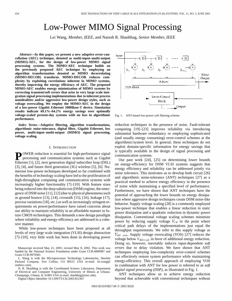
Fig. 1. ANT-based low-power soft filtering scheme.
reduction techniques in the presence of noise. Fault-tolerantcomputing [19]–[23] improves reliability via introducingsubstantial hardware redundancy or employing sophisticated(and usually energy consuming) error-control schemes at thealgorithmic/system level. In general, these techniques do notexploit domain-specific information for energy savings thatis typically available in the design of signal processing andcommunication systems.
Our past work [24], [25] on determining lower boundson energy-efficiency for DSM VLSI systems suggests thatenergy efficiency and reliability can be addressed jointly vianoise tolerance. This motivates us to develop both circuit [26]and algorithmic noise-tolerance (ANT) techniques [27] as apractical method to achieve energy efficiency in the presenceof noise while maintaining a specified level of performance.Furthermore, we have shown that ANT techniques have thepotential of approaching the lower bounds on energy dissipa-tion where aggressive design techniques create DSM noise-likebehavior. Supply voltage scaling [28] is a commonly employedlow-power technique that enables a linear reduction in staticpower dissipation and a quadratic reduction in dynamic powerdissipation. Conventional voltage scaling schemes minimizepower by reducing supply voltage to the point wherecritical path delays of the implementations just equal thethroughput requirements. We refer to this supply voltage as
. Supply voltage overscaling (VOS) [27] reduces thevoltage below in favor of additional energy reduction.Doing so, however, inevitably induces input-dependentsofterrors due to delay violation. We have shown that ANTtechniques employing low-complexity error-control schemescan effectively restore system performance while maintainingenergy-efficiency. This overall approach of employing VOSin combination with ANT for low power is referred to assoftdigital signal processing (DSP), as illustrated in Fig. 1.
ANT techniques allow us to achieve energy reductionbeyond that achievable with conventional techniques without
1063-8210/03$17.00 © 2003 IEEE
WANG AND SHANBHAG: LOW-POWER MIMO SIGNAL PROCESSING 435
loss in system performance. It works best in the context ofsignal processing and communication systems, where systemperformance metrics are measured in terms ofsignal-to-noiseratio (SNR) and/orbit-error rate (BER). In order to guaranteesubstantial energy savings, an ANT technique should be effec-tive in mitigating performance degradation while consumingminimal energy. Past work [27] reported aprediction-basederror-control (PEC) scheme that is suitable for narrowband fil-ters. For broadband signal processing, we proposed anadaptiveerror-cancellation(AEC) technique [29] via exploiting the cor-relation between the input signal and soft errors. In this paper,we build upon this AEC technique by proposing an AEC-basedadaptive filtering scheme and a multi-input–multi-output(MIMO)-AEC scheme for low-power MIMO systems. MIMOsignal processing is employed in many modern-day communi-cation systems, such as crosstalk suppression in gigabit Ethernet1000Base-T transceivers, multiuser detection and multi-an-tenna systems in wireless applications. Power dissipation isa critical concern for these systems due to intensive filteringcomputations being involved. The proposed MIMO-AECexploits the inherent correlations in MIMO systems via MIMOdecorrelating (MIMO-DECOR) to improve the energy-effi-ciency of AEC. We employ the proposed MIMO-AEC in thedesign of a low-power Gigabit Ethernet 1000Base-T device.Simulation results demonstrate 44.3%–25.2% reduction inenergy overhead due to MIMO-DECOR and 69.1%–64.2%energy savings over conventional implementations at the samealgorithmic performance.
The paper is organized as follows. In Section II, we reviewour past work on energy-optimum AEC. In Section III, wepresent the design strategies for AEC-based adaptive signalprocessing. In Section IV, we propose the MIMO-AECtechnique for MIMO systems. Simulation results of GigabitEthernet 1000Base-T transceivers are provided in Section V.
II. A DAPTIVE ERROR-CANCELLATION (AEC)
In this section, we present preliminaries regarding VOS andANT and review the past work on energy-optimum AEC (forbroadband soft DSP implementations.
A. Algorithmic Noise-Tolerance
VOS exploits the relationship between supply voltage and cir-cuit delay for power reduction. For the purpose of illustration,we assume that the critical path delay of a filter generating 22-bitoutputs is equal to 22 , where is the full adder delayat a voltage of . Thus, the minimal voltage neces-sary for correct operation is determined by ,where is the sample period of the input. If the supply voltageis overscaled to [where isthe VOS factor (VOSF)] such that ,then . This indicates that, while the filter stillfunctions correctly at the lower 18 least significant bits (LSBs)(assuming the use of LSB-first computation), the top four mostsignificant bits (MSBs) of the output will be in error providedinput patterns exciting the critical paths and other longer pathsare applied.
Past work [27], [29] has shown that soft errors due to VOScan be corrected by low-complexity error-control techniques re-ferred to as ANT. This leads to soft DSP implementations where
substantial energy reduction is made possible by VOS while thedesired level of system performance is restored by ANT. An ef-fective ANT technique is the one that is able to detect and cor-rect errors that may arise in a comparatively large VOS blockwithout incurring large overhead. The AEC technique [29] forbroadband signal processing exploits the statistical relationshipbetween the input and soft errors for error-control, as describedbelow.
B. Energy-Optimum AEC
In the presence of soft error , the output of an-tap VOS filter can be expressed as
(1)
where ’s are the coefficients of , is the error-freeoutput and is the input.
AEC employs a low-complexity error-cancellation filterthat estimates the value of soft error and then
subtracts it from the output to mitigate the performance degra-dation. We observe that is induced by the input samples
. Hence, it is possible togenerate a statistical replica of soft errors from input samplesby exploiting the correlation between the input signal and thesoft-error signal. Given the fact that such correlation may benonstationary due to variations in the process, temperature andinput statistics, one effective way to do so is to use theleastmean square(LMS) algorithm [30] that adaptively updates thecoefficients ’s of the error canceller , as follows:
(2)
(3)
(4)
where is the estimate of , denotes the estimationerror, is the complex conjugate of , is the stepsize, and 's are a control vector [32] of which theenergy-optimum choice will be discussed later. It can be shownthat by properly choosing the step sizeand ’s, we are able tominimize the mean-squared estimation error, which is expressedas . Thus, in the steady-state filtering opera-tion, the output of an AEC-based filter can be expressed as
(5)
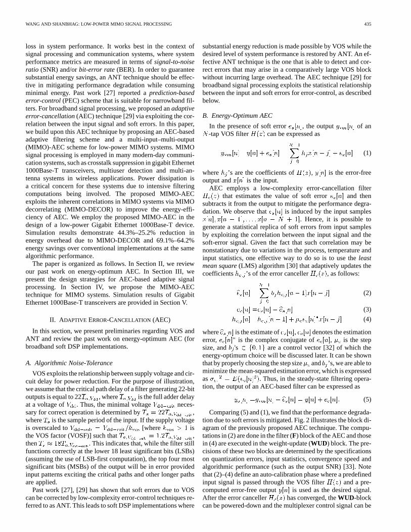
Comparing (5) and (1), we find that the performance degrada-tion due to soft errors is mitigated. Fig. 2 illustrates the block di-agram of the previously proposed AEC technique. The compu-tations in (2) are done in the filter (F) block of the AEC and thosein (4) are executed in the weight-update (WUD) block. The pre-cisions of these two blocks are determined by the specificationson quantization errors, input statistics, convergence speed andalgorithmic performance (such as the output SNR) [33]. Notethat (2)–(4) define an auto-calibration phase where a predefinedinput signal is passed through the VOS filter and a pre-computed error-free output is used as the desired signal.After the error canceller has converged, theWUD-blockcan be powered-down and the multiplexer control signal can be
436 IEEE TRANSACTIONS ON VERY LARGE SCALE INTEGRATION (VLSI) SYSTEMS, VOL. 11, NO. 3, JUNE 2003
Fig. 2. Proposed ANT technique based on adaptive error-cancellation.
flipped so that gets subtracted directly from the outputthereby cancelling out the soft errors.
The vector in (2) determines thetradeoff between system performance and achievable energysavings. Specifically, powers down theth tap ofwhich alleviates the AEC overhead. Doing so, however, maydegrade the effectiveness of error-cancellation. A systematicmethod has been proposed for deriving an energy-optimum so-lution that minimizes the energy dissipation of the AEC-based filter while being subject to a prespecified level of al-gorithmic performance. Using the Lagrange multiplier method[31], the optimum solution is obtained as [32]
if
if(6)
where is the optimumsensitivity vectorof the Lagrangemultiplier, the variance of the input signal andis the energy dissipation due to theth tap of . Giventhe coefficient , the value of can be estimated via theweighted multiplier energy model [32]. The energy-optimumlength of the resulting error canceller can beexpressed as
(7)
From (6), if the th tap of has a large coeffi-cient while consuming a relatively small energy . Oth-erwise, we can switch off theth tap of . It was shown [29]that if the th tap of the primary filter has a coefficientwith large magnitude, then the critical paths and other longerpaths (which generate MSBs) get excited easily thereby creatinga large soft-error component. This makes large which inturn implies . An important observation is that, as thebandwidth of increases, the predominant contribution tothe soft-error energy at the output will be from fewer taps of
. This is because wideband filters have a narrow impulseresponse. Thus, more ’s will be zero resulting in a smaller
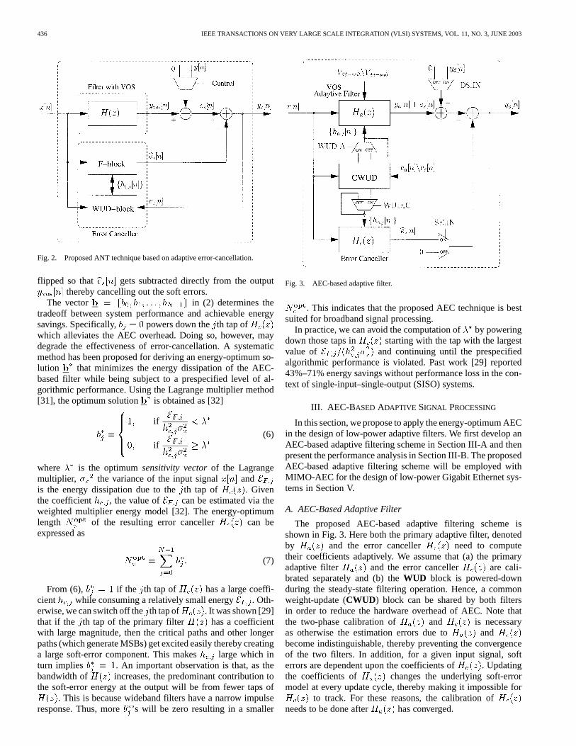
Fig. 3. AEC-based adaptive filter.
. This indicates that the proposed AEC technique is bestsuited for broadband signal processing.
In practice, we can avoid the computation ofby poweringdown those taps in starting with the tap with the largestvalue of and continuing until the prespecifiedalgorithmic performance is violated. Past work [29] reported43%–71% energy savings without performance loss in the con-text of single-input–single-output (SISO) systems.
III. AEC-BASED ADAPTIVE SIGNAL PROCESSING
In this section, we propose to apply the energy-optimum AECin the design of low-power adaptive filters. We first develop anAEC-based adaptive filtering scheme in Section III-A and thenpresent the performance analysis in Section III-B. The proposedAEC-based adaptive filtering scheme will be employed withMIMO-AEC for the design of low-power Gigabit Ethernet sys-tems in Section V.
A. AEC-Based Adaptive Filter
The proposed AEC-based adaptive filtering scheme isshown in Fig. 3. Here both the primary adaptive filter, denotedby and the error canceller need to computetheir coefficients adaptively. We assume that (a) the primaryadaptive filter and the error canceller are cali-brated separately and (b) theWUD block is powered-downduring the steady-state filtering operation. Hence, a commonweight-update (CWUD) block can be shared by both filtersin order to reduce the hardware overhead of AEC. Note thatthe two-phase calibration of and is necessaryas otherwise the estimation errors due to andbecome indistinguishable, thereby preventing the convergenceof the two filters. In addition, for a given input signal, softerrors are dependent upon the coefficients of . Updatingthe coefficients of changes the underlying soft-errormodel at every update cycle, thereby making it impossible for
to track. For these reasons, the calibration ofneeds to be done after has converged.
WANG AND SHANBHAG: LOW-POWER MIMO SIGNAL PROCESSING 437
The operation of AEC-based LMS adaptive filters consists ofthree phases, as described below with reference to Fig. 3:
1) Filter Calibration Phase: During this phase, the supplyvoltage is set to , control signals WUD_A and DS_INare ON, WUD_C and SE_IN are OFF and a predefined trainingsequence is fed into . Note that during this phase soft error
is always zero. Hence, the coefficients ’s of getupdated by the error signal between the filter outputand a precomputed desired signal , as follows:
(8)
(9)
(10)
2) AEC Calibration Phase:During this phase, the supplyvoltage is overscaled to (whose value is determinedby the algorithmic performance such as the output SNR [29]),control signals WUD_C, SE_IN and DS_IN are ON, whileWUD_A is OFF. Due to VOS, soft errors start to appear at theoutput of . The coefficients ’s of the energy-op-timum error canceller are computed according to
(11)
(12)
(13)
where is given by (7) and if in (6). Notethat the error signal in (12) contains residual error from thefirst phase [see (9)]. However, it will be shown later thathas a minor effect on the optimum configuration of asdescribed in (6) and (7).
3) Soft Filtering Phase:After has converged, thesupply voltage is kept at , control signal SE_IN isON while the others are OFF. The filter output can becomputed as
(14)
where and are given by (8) and (11), respectively,and is the soft error due to VOS. This starts the steady-state filtering operation where significant energy reduction isachieved via VOS while the required algorithmic performanceis guaranteed by AEC.
B. Performance Analysis
We now study the error-control performance of the proposedAEC-based adaptive filtering scheme. From (12), the errorsignal seen by in the AEC calibration phase is composedof soft error and the residual estimation errorfrom . However, it can be proved that the optimumWeiner–Hopf solutions for and are independentof each other.
To show this, we assume that the input is a zero-meanand uncorrelated random signal and denote as the de-sired signal for the adaptive filter . In the filter calibration
phase, we obtain the optimum coefficients ’s of as[30]
(15)
where is the variance of the input signal . Substitutingfrom (15) into (8) and (9), we obtain the residual estimation
error as
(16)
In the AEC calibration phase, due to the presence of nonzero, the optimum coefficients ’s of the error cancellercan be expressed as
(17)
where denotes the soft output error from the convergedVOS filter . Note that the residual estimation errorin the Weiner–Hopf solution is statistically orthogonal to theinput signal [30], i.e.,
(18)
Hence, ’s in (17) are an unbiased optimum solution evenif a nonzero is present.
The LMS calibrations given by (8)–(10) and (11)–(13) re-sult in filter coefficients that approach their Weiner–Hopf so-lutions. It can be easily shown that after has converged,the residual estimation error can be expressed as
(19)
where is given by (16) and denotes the input-de-pendent excess error which is statistically small.
From (12) and (19), the error canceller is in fact can-celling , as is orthogonal to the input signal
and therefore cannot be cancelled by . However, asis much smaller than , it has a minor effect on the
configuration of .In practical systems, variations over time in temperature and
physical channel parameters may occur which in turn will re-quire us to recalibrate and hence . The frequencyof these recalibrations will depend upon the rate at which tem-perature and channel parameters change. For Gigabit Ethernet1000Base-T systems of interest in this paper, the channel param-eters and temperature are more or less constant. This is becausethese systems are located indoors with well-controlled ambienttemperature. Hence, recalibration will be required on startup oronce in several days if at all. In any case, the AEC-based adap-tive filter can be recalibrated according to the procedure givenin Section III-A.
438 IEEE TRANSACTIONS ON VERY LARGE SCALE INTEGRATION (VLSI) SYSTEMS, VOL. 11, NO. 3, JUNE 2003
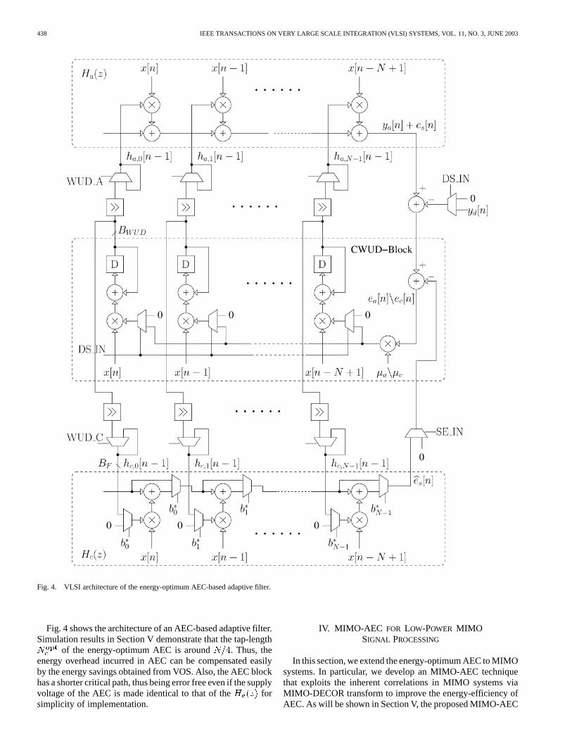
Fig. 4. VLSI architecture of the energy-optimum AEC-based adaptive filter.
Fig. 4 shows the architecture of an AEC-based adaptive filter.Simulation results in Section V demonstrate that the tap-length
of the energy-optimum AEC is around . Thus, theenergy overhead incurred in AEC can be compensated easilyby the energy savings obtained from VOS. Also, the AEC blockhas a shorter critical path, thus being error free even if the supplyvoltage of the AEC is made identical to that of the forsimplicity of implementation.
IV. MIMO-AEC FOR LOW-POWER MIMOSIGNAL PROCESSING
In this section, we extend the energy-optimum AEC to MIMOsystems. In particular, we develop an MIMO-AEC techniquethat exploits the inherent correlations in MIMO systems viaMIMO-DECOR transform to improve the energy-efficiency ofAEC. As will be shown in Section V, the proposed MIMO-AEC

WANG AND SHANBHAG: LOW-POWER MIMO SIGNAL PROCESSING 439
technique can achieve substantial energy savings in practicalMIMO systems such as Gigabit Ethernet 1000Base-T trans-ceivers. A matrix representation of MIMO systems is given inSection IV-A and the MIMO-AEC is proposed in Section IV-B.In Section IV-C, we derive the MIMO-DECOR transform forpractical MIMO systems.
A. MIMO Model
Consider a generic-input, -output MIMO system com-posed of adaptive or fixed-coefficient filters and expressedin matrix form as
(20)
where is the thinput sequence, is the co-efficient vector of the filter taking theth input and generatingthe th output, is the th output,and “ ” denotes the element-by-element convolution opera-tion, i.e., . A special caseof (20) is a system with a diagonal transfer matrix (i.e.,for ) representing independent SISO filtering operations,such as the channel equalizer in Gigabit Ethernet 1000Base-Ttransceivers (see Section V).
Henceforth, we refer to the filter with coefficient vectoras filter . Note that in practical MIMO systems the
filters in (20) usually exhibit certain correlations in frequencyor time domain. For example, the interference suppressionscheme in a 1000Base-T device (see Section V) contains 12near-end crosstalk (NEXT) cancellers, among which everythree cancellers share the same input. These three cancellershave similar impulse responses, as they are designed to cancelthree similar NEXT interferences which are induced by thesame input signal on three spatially correlated crosstalk paths.Exploiting these inherent correlations allows us to developeffective energy reduction techniques as discussed below.
B. MIMO-AEC
We now present the low-power MIMO-AEC technique forMIMO signal processing systems. Assume that all the filters
’s in (20) operate in parallel and have matched criticalpath delays. Energy reduction via VOS induces soft errors atall the filter outputs ’s. This necessitates a bank of errorcancellers, for which the Weiner–Hopf solution [30] is given by
(21)
where is the coefficient vector of the error canceller forthe filter , and is the soft error at theth output .From (20), contains soft-error components, i.e.,
(22)
where denotes the soft error induced by in theVOS filtering operation .
Assume that the input sequences ’s are zero-mean andfrom independent data sources, which is typical for practicalMIMO systems. Thus, in (22) is uncorrelated tofor , i.e., . Accordingly, the solu-tion of in (21) can be expressed as
(23)
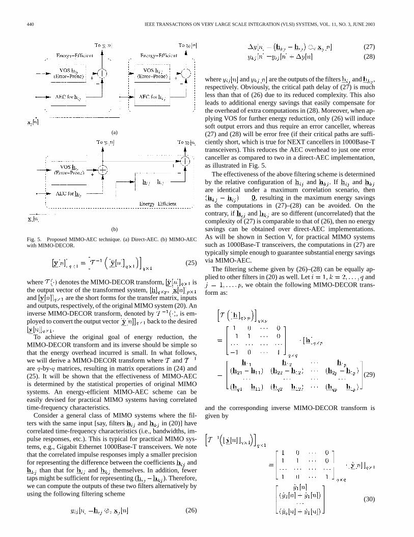
where is the variance of . Note that the result givenby (23) is the same as that for a SISO filter. Hence, we candecouple the error cancellers ’s and implement eachof them independently via the energy-optimum AEC given inSection III. We denote this approach asdirect-AEC, as shownin Fig. 5(a).
While the energy-optimum AEC guarantees the minimum en-ergy overhead for an individual error canceller, the direct-AECscheme consisting of independent error cancellers, one foreach VOS filter in (20), may not be energy-efficient. This is dueto the fact that the possible correlations among the original fil-ters ’s may introduce computational redundancies. In orderto further improve energy-efficiency, we propose an algorithmtransformation denoted as MIMO-DECOR. In contrast with thedirect-AEC, the AEC scheme employing MIMO-DECOR forenergy optimization is referred to as MIMO-AEC.
C. MIMO-DECOR
Decorrelating (DECOR) transform [35] was studied previ-ously for narrowband SISO filters. It employs the fact that thedifference between the adjacent coefficients of a filter is typi-cally less in magnitude, thereby requiring less hardware com-plexity and power dissipation in the implementation. The moti-vation for the MIMO-DECOR proposed in this paper is that forfilters in a MIMO system with correlated time-frequency char-acteristics (i.e., bandwidths, impulse responses, etc.), a smallerprecision and fewer taps might be sufficient for representing thedifference between these filters than those for themselves. Thus,we can employ the proposed MIMO-DECOR to shorten somecritical paths so that some filters in the MIMO system will be-come error free during VOS. This helps to reduce the numberof error cancellers, thereby reducing the overhead of noise-tol-erance. Note that the proposed MIMO-DECOR differs from theprevious work [35], [36] in that it is employed to reduce the cor-relations among the filters in a MIMO system. These filters canbe either wide-band or narrow-band.
In its most general form, the MIMO-DECOR can be ex-pressed as
(24)
440 IEEE TRANSACTIONS ON VERY LARGE SCALE INTEGRATION (VLSI) SYSTEMS, VOL. 11, NO. 3, JUNE 2003
(a)
(b)
Fig. 5. Proposed MIMO-AEC technique. (a) Direct-AEC. (b) MIMO-AECwith MIMO-DECOR.
(25)
where denotes the MIMO-DECOR transform, isthe output vector of the transformed system, ,and are the short forms for the transfer matrix, inputsand outputs, respectively, of the original MIMO system (20). Aninverse MIMO-DECOR transform, denoted by , is em-ployed to convert the output vector back to the desired
.To achieve the original goal of energy reduction, the
MIMO-DECOR transform and its inverse should be simple sothat the energy overhead incurred is small. In what follows,we will derive a MIMO-DECOR transform where andare -by- matrices, resulting in matrix operations in (24) and(25). It will be shown that the effectiveness of MIMO-AECis determined by the statistical properties of original MIMOsystems. An energy-efficient MIMO-AEC scheme can beeasily devised for practical MIMO systems having correlatedtime-frequency characteristics.
Consider a general class of MIMO systems where the fil-ters with the same input [say, filters and in (20)] havecorrelated time-frequency characteristics (i.e., bandwidths, im-pulse responses, etc.). This is typical for practical MIMO sys-tems, e.g., Gigabit Ethernet 1000Base-T transceivers. We notethat the correlated impulse responses imply a smaller precisionfor representing the difference between the coefficientsand
than that for and themselves. In addition, fewertaps might be sufficient for representing ( ). Therefore,we can compute the outputs of these two filters alternatively byusing the following filtering scheme
(26)
(27)
(28)
where and are the outputs of the filters and ,respectively. Obviously, the critical path delay of (27) is muchless than that of (26) due to its reduced complexity. This alsoleads to additional energy savings that easily compensate forthe overhead of extra computations in (28). Moreover, when ap-plying VOS for further energy reduction, only (26) will inducesoft output errors and thus require an error canceller, whereas(27) and (28) will be error free (if their critical paths are suffi-ciently short, which is true for NEXT cancellers in 1000Base-Ttransceivers). This reduces the AEC overhead to just one errorcanceller as compared to two in a direct-AEC implementation,as illustrated in Fig. 5.
The effectiveness of the above filtering scheme is determinedby the relative configuration of and . If andare identical under a maximum correlation scenario, then
, resulting in the maximum energy savingsas the computations in (27)–(28) can be avoided. On thecontrary, if and are so different (uncorrelated) that thecomplexity of (27) is comparable to that of (26), then no energysavings can be obtained over direct-AEC implementations.As will be shown in Section V, for practical MIMO systemssuch as 1000Base-T transceivers, the computations in (27) aretypically simple enough to guarantee substantial energy savingsvia MIMO-AEC.
The filtering scheme given by (26)–(28) can be equally ap-plied to other filters in (20) as well. Let , and
, we obtain the following MIMO-DECOR trans-form as:
(29)
and the corresponding inverse MIMO-DECOR transform isgiven by
(30)
WANG AND SHANBHAG: LOW-POWER MIMO SIGNAL PROCESSING 441
(a)
(b)
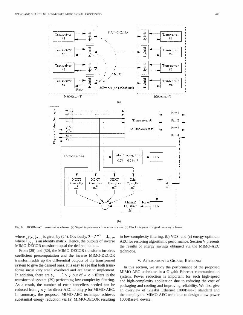
Fig. 6. 1000Base-T transmission scheme. (a) Signal impairments in one transceiver. (b) Block diagram of signal recovery scheme.
where is given by (24). Obviously, ,where is an identity matrix. Hence, the outputs of inverseMIMO-DECOR transform equal the desired outputs.
From (29) and (30), the MIMO-DECOR transform involvescoefficient precomputation and the inverse MIMO-DECORtransform adds up the differential outputs of the transformedsystem to give the desired ones. It is easy to see that both trans-forms incur very small overhead and are easy to implement.In addition, there are out of filters in thetransformed system (29) performing low-complexity filtering.As a result, the number of error cancellers needed can bereduced from for direct-AEC to only for MIMO-AEC.In summary, the proposed MIMO-AEC technique achievessubstantial energy reduction via (a) MIMO-DECOR resulting
in low-complexity filtering, (b) VOS, and (c) energy-optimumAEC for restoring algorithmic performance. Section V presentsthe results of energy savings obtained via the MIMO-AECtechnique.
V. APPLICATION TO GIGABIT ETHERNET
In this section, we study the performance of the proposedMIMO-AEC technique in a Gigabit Ethernet communicationsystem. Power reduction is important for such high-speedand high-complexity application due to reducing the cost ofpackaging and cooling and improving reliability. We first givean overview of Gigabit Ethernet 1000Base-T standard andthen employ the MIMO-AEC technique to design a low-power1000Base-T device.
442 IEEE TRANSACTIONS ON VERY LARGE SCALE INTEGRATION (VLSI) SYSTEMS, VOL. 11, NO. 3, JUNE 2003
A. 1000Base-T Transceivers
Gigabit Ethernet is a new generation of high-bandwidthdata interface over copper medium for local area networks(LAN). The 1000Base-T standard defines connections betweenswitches/repeaters and data terminal equipments (DTE) suchas desktop terminals. As illustrated in Fig. 6, the 1000Base-Ttransmission scheme specifies a 1000Mb/s, full duplex datathroughput achieved by using four pairs of wire in Cate-gory 5 (CAT-5) cable, each pair transmitting a 250Mb/sdata stream encoded into a four-dimension (4-D) five-level
pulse amplitude modulation (4-D PAM-5)signal constellation. The interested reader is referred to [1] fora detailed discussion of 4-D PAM-5 modulation scheme.
Each 1000Base-T device contains four identical transceivers,one for each pair of physical wire. The bidirectional data trans-mission on the same wire is made possible by hybrid circuits.On the transmit side, the outgoing data stream is processed by apulse shaping filter to limit the high-frequencyradiation of the transmitted signal within FCC requirements. Onthe receive side, each receiver confronts a physical channel ofminimum 100m CAT-5 cable. As shown in Fig. 6(a), the threemajor causes of signal distortion encountered are propagationloss (due to channel attenuation), echo noise (generated by aself-returned signal due to impedance mismatch in hybrid cir-cuits) and NEXT noise (caused by near-end crosstalk betweenadjacent wires). The detailed description of physical mecha-nisms of these impairments can be found in [37]. The IEEEStandard 802.3ab [1] specifies the models for the worst-casenoise environment as
(31)
(32)
(33)
where is the frequency expressed in MHz, ,and , all expressed in dB/100 m, are the squared
magnitude of the propagation loss, NEXT, and echo transferfunction, respectively.
The 1000Base-T data transmission requires a BER10 .Using 4-D PAM-5 modulation scheme, the SNR at the slicer forachieving this BER is 19.3 dB. To overcome considerable signaldistortion caused by echo, NEXT, cable attenuation and disper-sion, advanced digital signal processing and filtering techniquesare needed for signal recovery. Fig. 6(b) depicts the block dia-gram of a 1000Base-T device which consists of four identicaltransceivers operating simultaneously at 125 Mbaud. At eachreceiver, the digital output of the A/D converter is first filteredby a feed-forward equalizer (FFE) to remove the intersymbolinterference (ISI) introduced by the channel. As each receivedsignal is also corrupted by one echo and three NEXT interfer-ences from the adjacent wires, one echo canceller and threeNEXT cancellers are needed correspondingly to perform inter-ference suppression. In total, each 1000Base-T device requiresfour FFEs, four echo cancellers and twelve NEXT cancellers,all of which are LMS adaptive filters. This involves intensive
TABLE IDESIGNSPECIFICATIONS FOR THEENERGY-OPTIMUM AEC-BASED FILTERS
TABLE IIDESIGN SPECIFICATIONS ANDENERGY SAVINGS FOR THEDIFFERENTIAL
NEXT CANCELLERS USING MIMO-DECOR
filtering operations which necessitate effective energy reductiontechniques to alleviate power dissipation.
B. Simulation Results
We describe the signal recovery scheme on the receive side ofa 1000Base-T device [see Fig. 6(b)] as a MIMO system, whichis expressed as
(34)
where is the recovered 4-D PAM-5signal, and are the transmitted and received signals,respectively, at theth transceiver, , , and denote theFFE, echo canceller and NEXT canceller (to cancel the NEXTinterference generated by theth transmitter), respectively, forthe th receiver. Note that the first term on the right side of (34)represents channel equalization which involves independentSISO filtering, whereas the second term describes the MIMOinterference suppression scheme. In what follows, we employthe proposed AEC to reduce the power dissipation of signalrecovery scheme (34). In particular, we apply the MIMO-AECfor the MIMO interference suppression scheme.
We assume that the SNR requirements for the FFE, echocancellation and NEXT cancellation are 25 dB, 28 dB, and30 dB, respectively. This results in a 21 dB SNR at ,which is 1.7 dB higher than the minimum of 19.3 dB necessaryfor achieving a BER of 10 . From (34), the FFE and echocancellation involve independent SISO filtering operations,
WANG AND SHANBHAG: LOW-POWER MIMO SIGNAL PROCESSING 443
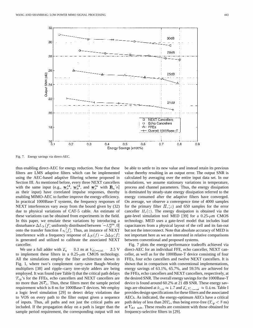
Fig. 7. Energy savings via direct-AEC.
thus enabling direct-AEC for energy reduction. Note that thesefilters are LMS adaptive filters which can be implementedusing the AEC-based adaptive filtering scheme proposed inSection III. As mentioned before, every three NEXT cancellerswith the same input (e.g., , , and withas their input) have correlated impulse responses, therebyenabling MIMO-AEC to further improve the energy-efficiency.In practical 1000Base-T systems, the frequency responses ofNEXT interferences vary away from the bound given by (32)due to physical variations of CAT-5 cable. An estimate ofthese variations can be obtained from experiments in the field.In this paper, we emulate these variations by introducing adisturbance uniformly distributed betweenonto the transfer function . Thus, an instance of NEXTinterference with a frequency response ofis generated and utilized to calibrate the associated NEXTcanceller.
We use a full adder with ns at Vto implement these filters in a 0.25-m CMOS technology.All the simulations employ the filter architecture shown inFig. 1, where two’s complement carry–save Baugh–Wooleymultipliers [38] and ripple–carry tree-style adders are beingemployed. It was found (see Table I) that the critical path delays
’s for the FFEs, echo cancellers and NEXT cancellers areno more than 26 . Thus, these filters meet the sample periodrequirement which is 8 ns for 1000Base-T devices. We employa logic level simulation [29] to detect delay violations dueto VOS on every path to the filter output given a sequenceof inputs. Thus, all paths and not just the critical paths areincluded. If the propagation delay on a path is larger than thesample period requirement, the corresponding output will not
be able to settle to its new value and instead retain its previousvalue thereby resulting in an output error. The output SNR iscalculated by averaging over the entire input data set. In oursimulations, we assume stationary variations in temperature,process and channel parameters. Thus, the energy dissipationis dominated by steady-state energy dissipation referred to theenergy consumed after the adaptive filters have converged.On average, we observe a convergence time of 4000 samplesfor the primary filter and 650 samples for the errorcanceller . The energy dissipation is obtained via thegate-level simulation tool MED [39] for a 0.25-m CMOStechnology. MED uses a gate-level model that includes loadcapacitances from a physical layout of the cell and its fan-outbut not the interconnect. Note that absolute accuracy of MED isnot important here as we are interested in relative comparisonsbetween conventional and proposed systems.
Fig. 7 plots the energy-performance tradeoffs achieved viadirect-AEC for an individual FFE, echo canceller, NEXT can-celler, as well as for the 1000Base-T device consisting of fourFFEs, four echo cancellers and twelve NEXT cancellers. It isshown that in comparison with conventional implementations,energy savings of 63.1%, 65.7%, and 59.5% are achieved forthe FFEs, echo cancellers and NEXT cancellers, respectively, atthe desired SNR. The overall energy savings for the 1000Base-Tdevice is found around 60.2% at 21 dB SNR. These energy sav-ings are obtained at and ns. Table Iprovides design specifications for these filters and the associatedAECs. As indicated, the energy-optimum AECs have a criticalpath delay of less than 20, thus being error-free ( ns)at . These results are consistent with those obtained forfrequency-selective filters in [29].
444 IEEE TRANSACTIONS ON VERY LARGE SCALE INTEGRATION (VLSI) SYSTEMS, VOL. 11, NO. 3, JUNE 2003
Fig. 8. Energy savings via MIMO-AEC.
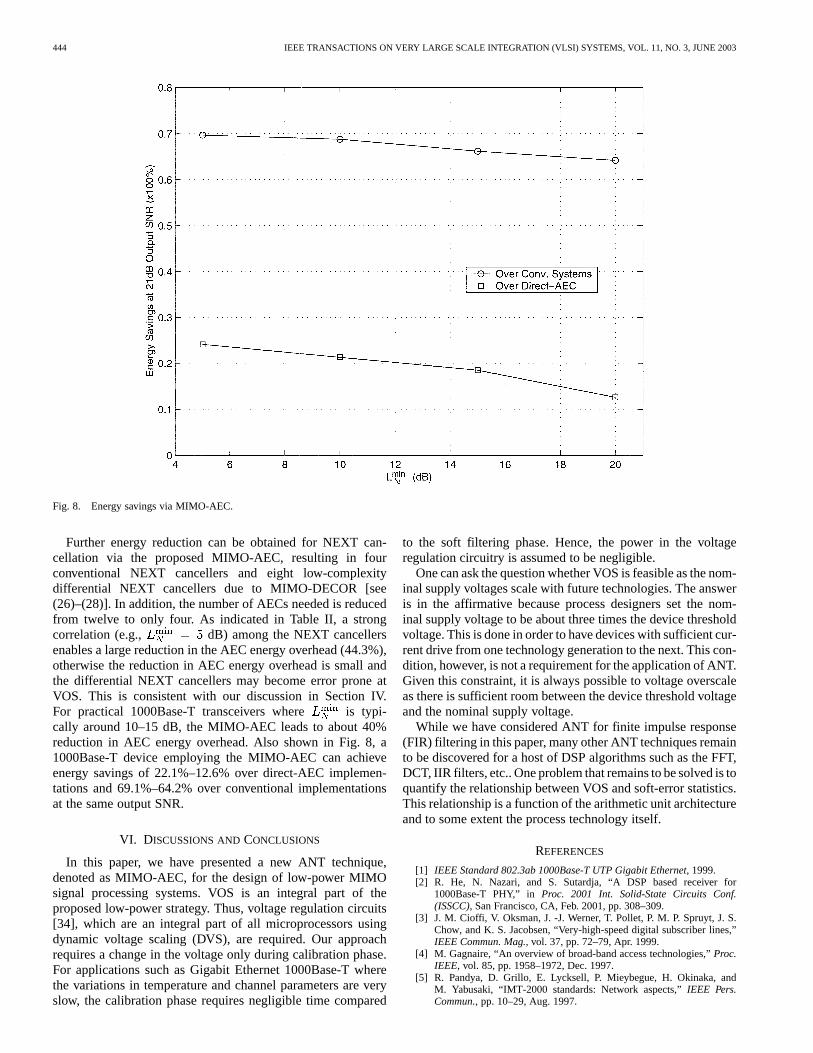
Further energy reduction can be obtained for NEXT can-cellation via the proposed MIMO-AEC, resulting in fourconventional NEXT cancellers and eight low-complexitydifferential NEXT cancellers due to MIMO-DECOR [see(26)–(28)]. In addition, the number of AECs needed is reducedfrom twelve to only four. As indicated in Table II, a strongcorrelation (e.g., dB) among the NEXT cancellersenables a large reduction in the AEC energy overhead (44.3%),otherwise the reduction in AEC energy overhead is small andthe differential NEXT cancellers may become error prone atVOS. This is consistent with our discussion in Section IV.For practical 1000Base-T transceivers where is typi-cally around 10–15 dB, the MIMO-AEC leads to about 40%reduction in AEC energy overhead. Also shown in Fig. 8, a1000Base-T device employing the MIMO-AEC can achieveenergy savings of 22.1%–12.6% over direct-AEC implemen-tations and 69.1%–64.2% over conventional implementationsat the same output SNR.
VI. DISCUSSIONS ANDCONCLUSIONS
In this paper, we have presented a new ANT technique,denoted as MIMO-AEC, for the design of low-power MIMOsignal processing systems. VOS is an integral part of theproposed low-power strategy. Thus, voltage regulation circuits[34], which are an integral part of all microprocessors usingdynamic voltage scaling (DVS), are required. Our approachrequires a change in the voltage only during calibration phase.For applications such as Gigabit Ethernet 1000Base-T wherethe variations in temperature and channel parameters are veryslow, the calibration phase requires negligible time compared
to the soft filtering phase. Hence, the power in the voltageregulation circuitry is assumed to be negligible.
One can ask the question whether VOS is feasible as the nom-inal supply voltages scale with future technologies. The answeris in the affirmative because process designers set the nom-inal supply voltage to be about three times the device thresholdvoltage. This is done in order to have devices with sufficient cur-rent drive from one technology generation to the next. This con-dition, however, is not a requirement for the application of ANT.Given this constraint, it is always possible to voltage overscaleas there is sufficient room between the device threshold voltageand the nominal supply voltage.
While we have considered ANT for finite impulse response(FIR) filtering in this paper, many other ANT techniques remainto be discovered for a host of DSP algorithms such as the FFT,DCT, IIR filters, etc.. One problem that remains to be solved is toquantify the relationship between VOS and soft-error statistics.This relationship is a function of the arithmetic unit architectureand to some extent the process technology itself.
REFERENCES
[1] IEEE Standard 802.3ab 1000Base-T UTP Gigabit Ethernet, 1999.[2] R. He, N. Nazari, and S. Sutardja, “A DSP based receiver for
1000Base-T PHY,” inProc. 2001 Int. Solid-State Circuits Conf.(ISSCC), San Francisco, CA, Feb. 2001, pp. 308–309.
[3] J. M. Cioffi, V. Oksman, J. -J. Werner, T. Pollet, P. M. P. Spruyt, J. S.Chow, and K. S. Jacobsen, “Very-high-speed digital subscriber lines,”IEEE Commun. Mag., vol. 37, pp. 72–79, Apr. 1999.
[4] M. Gagnaire, “An overview of broad-band access technologies,”Proc.IEEE, vol. 85, pp. 1958–1972, Dec. 1997.
[5] R. Pandya, D. Grillo, E. Lycksell, P. Mieybegue, H. Okinaka, andM. Yabusaki, “IMT-2000 standards: Network aspects,”IEEE Pers.Commun., pp. 10–29, Aug. 1997.
WANG AND SHANBHAG: LOW-POWER MIMO SIGNAL PROCESSING 445
[6] R. D. Carsello, R. Meidan, S. Allpress, F. O’Brien, J. A. Tarallo, N.Ziesse, A. Arunachalam, J. M. Costa, E. Berruto, R. C. Kirby, A.Maclatchy, F. Watanabe, and H. Xia, “IMT-2000 standards: Radioaspects,”IEEE Pers. Commun., pp. 30–40, Aug. 1997.
[7] A. P. Chandrakasan and R. W. Brodersen, “Minimizing power consump-tion in digital CMOS circuits,”Proc. IEEE, vol. 83, pp. 498–523, Apr.1995.
[8] J. D. Meindl, “Low power microelectronics: Retrospect and prospect,”Proc. IEEE, vol. 83, pp. 619–635, Apr. 1995.
[9] D. A. Parker and K. K. Parhi, “Low-area/power parallel FIR digital filterimplementations,”J. VLSI Signal Processing, vol. 17, pp. 75–92, Sept.1997.
[10] B. Davari, R. H. Dennard, and G. G. Shahidi, “CMOS scaling for high-performance and low power—The next ten years,”Proc. IEEE, vol. 83,pp. 595–606, Apr. 1995.
[11] K. L. Shepard and V. Narayanan, “Noise in deep submicron digitaldesign,” inProc. ’96 IEEE/ACM Int. Conf. Computer-Aided Design,(ICCAD), San Jose, CA, Nov. 1996, pp. 524–531.
[12] P. Larsson and C. Svensson, “Noise in digital dynamic CMOS circuits,”IEEE J. Solid-State Circuits, vol. 29, pp. 655–662, June 1994.
[13] A. Kabbani and A. J. Al-Khalili, “Estimation of ground bounce effectson CMOS circuits,”IEEE Trans. Comp. Packag. Technol., vol. 22, pp.316–325, June 1999.
[14] H. H. Chen and D. D. Ling, “Power supply noise analysis methodologyfor deep-submicron VLSI chip design,” inProc. 1997 Design Automa-tion Conf., Anaheim, CA, June 1997, pp. 638–643.
[15] Y. Eo, W. R. Eisenstadt, J. Y. Jeong, and O. K. Kwon, “A new on-chipinterconnect crosstalk model and experimental verification for CMOSVLSI circuit design,” IEEE Trans. Electron Devices, vol. 47, pp.129–140, Jan. 2000.
[16] K. Joardar, “A simple approach to modeling cross-talk in integrated cir-cuits,” IEEE J. Solid-State Circuits, vol. 29, pp. 1212–1219, Oct. 1994.
[17] M. C. Johnson, D. Somasekhar, and K. Roy, “Models and algorithmsfor bounds on leakage in CMOS circuits,”IEEE Trans. Computer-AidedDesign, vol. 18, pp. 714–725, June 1999.
[18] S. Natarajan, M. A. Breuer, and S. K. Gupta, “Process variations andtheir impact on circuit operation,” inProc. of Int. Symp. Defect and FaultTolerance VLSI Syst., Austin, TX, Nov. 1998, pp. 73–81.
[19] T. R. N. Rao and E. Fujiwara,Error-Control Coding for Computer Sys-tems. Englewood Cliffs, NJ: Prentice-Hall, 1989.
[20] G. R. Redinbo, “Generalized algorithm-based fault tolerance: Errorcorrection via Kalman estimation,”IEEE Trans. Comput., vol. 47, pp.639–655, June 1998.
[21] R. Karri, “Fault-tolerant VLSI systems,”IEEE Trans. Rel., vol. 48, pp.106–107, June 1999.
[22] Y. Y. Chen, S. J. Upadhyaya, and C. H. Cheng, “A comprehensive recon-figuration scheme for fault-tolerant VLSI/WSI array processors,”IEEETrans. Comput., vol. 46, pp. 1363–1371, Dec. 1997.
[23] C. Bolchini, G. Buonanno, D. Sciuto, and R. Stefanelli, “An improvedfault tolerant architecture at CMOS level,” inProc. Int. Symp. CircuitsSyst., vol. 4, Hong Kong, June 1997, pp. 2737–2740.
[24] N. R. Shanbhag, “A mathematical basis for power-reduction in digitalVLSI systems,”IEEE Trans. Circuits Syst. II, vol. 44, pp. 935–951, Nov.1997.
[25] R. Hedge and N. R. Shanbhag, “Toward achieving energy-efficiencyin presence of deep submicron noise,”IEEE Trans. VLSI, vol. 8, pp.379–391, Aug. 2000.
[26] L. Wang and N. R. Shanbhag, “An energy-efficient, noise-tolerantdynamic circuit technique,”IEEE Trans. Circuits Syst. II, vol. 47, pp.1300–1306, Nov. 2000.
[27] R. Hegde and N. R. Shanbhag, “Soft digital signal processing,”IEEETrans. VLSI Syst., vol. 9, pp. 813–823, Dec. 2001.
[28] R. Gonzalez, B. M. Gordon, and M. A. Horowitz, “Supply and thresholdvoltage scaling for low power CMOS,”IEEE J. Solid-State Circuits, vol.32, pp. 1210–1216, Aug. 1997.
[29] L. Wang and N. R. Shanbhag, “Low-power filtering via adaptive error-concellation,”IEEE Trans. Signal Process, vol. 51, pp. 575–583, Feb.2003.
[30] S. Haykin,Adaptive Filter Theory. Englewood Cliffs, NJ: Prentice-Hall, 1996.
[31] D. P. Bertsekas,Nonlinear Programming. Boston, MA: Athena Scien-tific, 1995.
[32] M. Goel and N. R. Shanbhag, “Dynamic algorithm transformations forlow-power reconfigurable adaptive equalizer,”IEEE Trans. Signal Pro-cessing, vol. 47, pp. 2821–2832, Oct. 1999.
[33] A. V. Oppenheim and R. W. Schafer,Discrete-Time Signal Pro-cessing. Englewood Cliffs, NJ: Prentice-Hall, 1994.
[34] G. Y. Wei and M. A. Horowitz, “A full digital, energy-efficient, adap-tive power-supply regulator,”IEEE J. Solid-State Circuits, vol. 34, pp.520–528, Apr. 1999.
[35] S. Ramprasad, N. R. Shanbhag, and I. N. Hajj, “Decorrelating (DECOR)transformations for low-power digital filters,”IEEE Trans. Circuits Syst.II , vol. 45, pp. 776–788, June 1999.
[36] N. Sankarayya, K. Roy, and D. Bhattacharya, “Algorithms for lowpower and high speed FIR filter realization using differential coeffi-cients,”IEEE Trans. Circuits Syst. II, vol. 44, pp. 488–497, June 1997.
[37] J. Kadambi, I. Crayford, and M. Kalkunte,Gigabit Ethernet—Migratingto High Bandwidth LAN’s. Englewood Cliffs, NJ: Prentice-Hall, 1998.
[38] C. R. Baugh and B. A. Wooley, “A two’s complement parallel array mul-tiplication algorithm,”IEEE Trans. Comput., vol. C-22, pp. 1045–1047,Dec. 1973.
[39] M. G. Xakellis and F. N. Najm, “Statistical estimation of the switchingactivity in digital circuits,” inProc. 31st Design Automation Conf., SanDiego, CA, June 1994, pp. 728–733.
[40] S. Gupta and F. N. Najm, “Power modeling for high-level power estima-tion,” IEEE Trans. VLSI, vol. 8, pp. 18–29, Feb. 2000.
Lei Wang (M’01) received the B.Engr. and M.Engr.degrees from Tsinghua University, Beijing, China, in1992 and 1996, respectively, and the Ph.D. degreefrom the University of Illinois at Urbana-Champaign,in 2001. His Ph.D. research focus was on explorationof performance limits of deep submicron very largescale integration (VLSI) systems and development ofnoise-tolerance techniques for low-power signal pro-cessing and computing systems.
In Summer 1999, he was with Microprocessor Re-search Laboratory, Intel Corporation, Hillsboro, OR,
where his work involved development of high-speed and noise-tolerant VLSIdesign techniques. In 2001, he joined Hewlett-Packard Microprocessor Tech-nology Laboratories, Fort Collins, CO. His current research interests includedesign and implementation of low-power, high-speed and noise-tolerance VLSIsystems.
Naresh R. Shanbhag (M’88–SM’98) receivedthe B. Tech. degree from the Indian Institute ofTechnology, New Delhi, India, the M.S. degree fromWright State University, Dayton, OH, and the Ph.D.degree from the University of Minnesota, MN, allin electrical engineering, in 1988, 1990, and 1993,respectively.
From July 1993 to August 1995, he was withAT&T Bell Laboratories, Murray Hill, NJ, where hewas responsible for the development of very largescale integration (VLSI) algorithms, architectures,
and implementation of broadband data communications transceivers. Inparticular, he was the Lead-Chip Architect for AT&T’s 51.84-Mb/s transceiverchips over twisted-pair wiring for asynchronous transfer mode (ATM)-LANand broadband access chip-sets. Since August 1995, he has been with theDepartment of Electrical and Computer Engineering and the CoordinatedScience Laboratory, University of Illinois-Urbana, where he is presentlyan Associate Professor and Director of the Illinois Center for IntegratedMicrosystems. At the University of Illinois, he founded the VLSI InformationProcessing Systems (ViPS) Group, whose charter is to explore issues related tolow-power, high-performance, and reliable integrated circuit implementationsof broad-band communications and digital signal processing systems spanningthe algorithmic, architectural and circuit domains. He has published more than90 journal articles, book chapters, and conference publications in this areaand holds three U.S. patents. He is also a coauthor of the research monographPipelined Adaptive Digital Filters(Norwell, MA: Kluwer, 1994).
Dr. Shanbhag received the the 2001 IEEE TRANSACTIONS ONVERY LARGE
SCALE INTEGRATION (VLSI) SYSTEMSBest Paper Award, the 1999 IEEE LeonK. Kirchmayer Best Paper Award, the 1999 Xerox Faculty Award, the NationalScience Foundation CAREER Award in 1996, and the 1994 Darlington BestPaper Award from the IEEE Circuits and Systems Society. From July 1997through 2001, he was a Distinguished Lecturer for the IEEE Circuits and Sys-tems Society. From 1997 to 1999, he served as an Associate Editor for the IEEETRANSACTION ON CIRCUITS AND SYSTEMS—PART: II A NALOG AND DIGITAL
SIGNAL PROCESSING. He has served on Technical Program Committees of var-ious international conferences.