Embed Size (px)
Citation preview
Low Noise, Low Power Capacitive-Coupling Quadrature Voltage-Controlled
Oscillator for Phase-Locked Loops
by
Feng Zhao
A dissertation submitted to the Graduate Faculty of
Auburn University
in partial fulfillment of the
requirements for the Degree of
Doctor of Philosophy
Auburn, Alabama
December 8, 2012
Keywords: quadrature voltage-controlled oscillator (QVCO), phase-locked loop (PLL),
phase noise, phase accuracy, bi-modal oscillation
Copyright 2012 by Feng Zhao
Approved by
Fa Foster Dai, Chair, Professor of Electrical and Computer Engineering
Guofu Niu, Alumni Professor of Electrical and Computer Engineering
Bogdan M. Wilamowski, Professor of Electrical and Computer Engineering
Stanley J. Reeves, Professor of Electrical and Computer Engineering
ii
Abstract
This dissertation presents the analytical results and design details of two quadrature
voltage-controlled oscillators (QVCO). It uses capacitive quadrature-coupling technique
to couple two voltage-controlled oscillator (VCO) cores. The proposed capacitive-
coupling QVCO (CC-QVCO) architecture provides the advantage of low phase noise
performance and elimination of the bi-modal oscillation. Different from conventional
quadrature-coupling mechanism with active devices, CC-QVCO utilizes noiseless
capacitors to form QVCO allowing shaped gate voltage and reduced thermal noise.
A differential Colpitts CC-QVCO with enhanced swing is proposed to offer
excellent phase noise performance under a 0.6-V power supply. It achieves 4.5dB lower
phase noise than its single-phase counterpart at 3-MHz offset. Optimized capacitive
coupling combined with source inductive enhance-swing technique enables low power
and low phase noise simultaneously. The QVCO achieves a measured phase noise of -
132.3dBc/Hz @ 3MHz offset with a center frequency of 5.6GHz and consumes 4.2mW
from a 0.6-V supply. This performance corresponds to a Figure-of-Merit (FoM) of
191.5dB. Due to the inherent phase shift in the proposed quadrature-coupling path, the
problem associated with ±90º phase ambiguity between the quadrature outputs has been
avoided.
Capacitive-coupling technique is also applied to classic NMOS cross-coupled VCO
iii
with current tail to demonstrate its advantages over other quadrature-coupling technique.
The problem of phase ambiguity for this QVCO has also been successfully avoided by
the inherent leading phase shifter. Silicon implementations and measurement results of
this CC-QVCO and another class-C mode top-series QVCO (TS-QVCO) for comparison
have been discussed. The CC-QVCO has been fabricated in a 0.13µm CMOS technology
and occupies an area of 1.0×0.35mm2. With 1.2-V supply voltage, it achieves 0.23-0.91°
phase error in the frequency range of 4.3-5.27GHz. It demonstrates the effectiveness of
the capacitive-coupling technique for wide frequency range quadrature signal generation
and low phase noise performance.
ΣΔ modulator based fractional-N PLL is widely used to produce frequency reference
for wireless communication systems. Quantization noise caused by ΣΔ modulator will
degrade the phase noise spectrum at the PLL output, and the situation becomes worse
when the loop is nonlinear. Techniques and structures for noise improvement have been
proposed to address the problem of noise degradation caused by ΣΔ modulator. Also
included is the design of a wideband PLL with power optimized divider. An intuitive but
useful power optimization methodology is proposed for dividers.
iv
Acknowledgments
I have been extremely fortunate to be a graduate student in the ECE department at
Auburn University and work closely with my academic advisor, Prof. Fa Foster Dai. I
would like to express my deepest gratitude and appreciation to him for his invaluable
guidance, discussions, encouragement, and assistance during my study and research. His
instruction and motivation lead to the completion of this research work. He is also an
important friend to me in my personal lives and career because he is like a beacon,
lighting up my way.
I would like to take this opportunity to thank my committee members, Prof. Bogdan
M. Wilamowski, Prof. Stanley J. Reeves, and Prof. Guofu Niu for taking their valuable
times out of their busy schedule to serve in the committee. I want to thank Prof. Bogdan
Wilamowski for leading me into the area of neural networks and Prof. Stanley Reeves for
the technical discussions in DSP area. I would like to express my gratitude to Prof. Guofu
Niu for his invaluable discussion and advice to my career. I would also like to thank Dr.
Stuart M. Wentworth for consolidating my understanding of microwave operation and
Mike Palmer for his help in chip bonding. I would like to thank Dr. David Irwin and Dr.
Richard Jaeger for their guidance and discussions during my PhD study.
I extend my thanks to those great friends who have made graduate study life
intellectually and socially enriched. I would like to express my sincere gratitude to the
v
friendship of Xueyang Geng, Desheng Ma, Xuefeng Yu, Yuan Yao, Yuehai Jin, Jianjun
Yu, Joseph Cali, Michael Pukish, Xin Jin, Kaijun Li, Zachary Hubbard, Siyu Yang, Rong
Jiang, Hechen Wang, and Zhan Su for their accompanying through many difficult and
delighted times.
All of the work was made possible by the love and encouragement of my family. I
would like to appreciate my parents and family members for their support. Finally I
would like to express my cordial appreciation to my wife Yumei Tang and my Son Kevin
K. Zhao for their continuous love and support.
vi
Table of Contents
Abstract ............................................................................................................................... ii
Acknowledgments.............................................................................................................. iv
List of Figures .................................................................................................................... ix
List of Tables ................................................................................................................... xiii
Chapter 1 Introduction ........................................................................................................ 1
1.1 Prior Art of QVCO Structures .............................................................................. 5
1.2 Analysis of QVCO for Deterministic Quadrature Outputs .................................. 6
1.3 Phase-Locked Loop Frequency Synthesizer ........................................................ 9
1.4 Outline and Contribution .................................................................................... 12
Chapter 2 A 0.6-V Low-Phase Noise CC-QVCO with Enhanced Swing ........................ 14
2.1 Introduction ........................................................................................................ 14
2.2 CC-QVCO with Noise Reduction and Stable Oscillation .................................. 17
2.2.1 Architecture of the CC-QVCO ................................................................... 17
2.2.2 Colpitts VCO Core with Gm-Enhancement ................................................ 19
2.2.3 Noise Reduction for the CC-QVCO ........................................................... 26
2.2.4 Optimization of Capacitive Coupling ......................................................... 30
2.2.5 Intrinsic Phase Shift to Avoid Phase Ambiguity ........................................ 32
2.2.6 Quadrature Inaccuracy ................................................................................ 40
2.3 Implementation and Measured Results .............................................................. 41
2.4 Conclusions ........................................................................................................ 47
Chapter 3 A 0.23-0.91° 4.3-5.27GHz NMOS LC CC-QVCO without Bi-Modal
Oscillation ......................................................................................................................... 48
3.1 Introduction ........................................................................................................ 48
3.2 Important Aspects of QVCO and Prior QVCO Structures ................................ 49
vii
3.3 CC-QVCO with Leading Phase Delay ............................................................... 55
3.3.1 Linear Model of the CC-QVCO and Start-up Conditions .......................... 56
3.3.2 Mode Rejection for Stable Operation ......................................................... 61
3.4 Design and Simulation Results of a 5.6GHz CC-QVCO ................................... 64
3.4.1 Design Procedure of a CC-QVCO .............................................................. 64
3.4.2 Choice of Quadrature Coupling Factor m and Phase Delay ....................... 68
3.4.3 Phase Noise and Phase Error with Current Bias ......................................... 69
3.4.4 Class-C Mode TS-QVCO for Comparison ................................................. 73
3.4.5 Performance Tolerance to Voltage and Temperature Variations ............... 76
3.5 Implementation and Measurement Results ........................................................ 79
3.5.1 Upconversion Mixer and IF Baseband Signal Generation ......................... 80
3.5.2 Phase Noise and Frequency Range ............................................................. 82
3.5.3 Phase Accuracy ........................................................................................... 84
3.6 Conclusion .......................................................................................................... 85
Chapter 4 Quantization Noise Reduction Techniques for Fractional-N PLL ................... 87
4.1 Introduction ........................................................................................................ 87
4.2 ΣΔ Modulators and Noise Folding from Nonlinearity ....................................... 90
4.2.1 ΣΔ Modulator Structures and Phase Noise Contribution ............................ 90
4.2.2 Nonlinearity Analysis for ΣΔ Modulators .................................................. 94
4.2.3 Discussion of Simple Noise Reduction Techniques ................................... 96
4.3 Proposed Fractional-N PLL with Noise Cancellation ........................................ 97
4.4 Conclusion ........................................................................................................ 101
Chapter 5 A Wide-Band Integer-N PLL Design............................................................. 102
5.1 Introduction ...................................................................................................... 102
5.2 Analysis of Bandgap Reference for Current Generation ................................. 105
5.3 Circuit Design .................................................................................................. 107
5.3.1 VCO with Extended Frequency Range ..................................................... 107
5.3.2 Power and Speed Optimization for DTC .................................................. 109
5.3.3 Design Divide-by-2/3 and MMD .............................................................. 113
viii
5.4 Experimental Results of the Wide-Band PLL .................................................. 115
5.4.1 Phase Noise and Frequency Tuning Range .............................................. 115
5.4.2 Output Spectrum and Lock Time .............................................................. 116
5.5 Conclusion ........................................................................................................ 117
Chapter 6 Summary and Future Work ............................................................................ 119
6.1 Summary of the Works .................................................................................... 119
6.2 Future Work ..................................................................................................... 120
Bibliography ................................................................................................................... 122
ix
List of Figures
Fig. 1.1 A radar transceiver with image rejection capability. ............................................. 1
Fig. 1.2 Typical QVCO structure. ....................................................................................... 3
Fig. 1.3 Prototype circuits of VCO cores and coupling circuit for QVCO: (a) parallel
coupling, (b) back-gate coupling [10], (c) transformer coupling [9], (d) 2nd
-harmonic
coupling [2] [11] [12], and (e) top-series coupling [8]. Components in dashed boxes are
used for quadrature coupling. The connections at Q stage are similar to I stage with I+
coupled to Q- and I- coupled to Q+. For simplicity, the bias circuitry is not shown. ........ 4
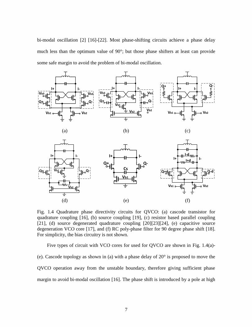
Fig. 1.4 Quadrature phase directivity circuits for QVCO: (a) cascode transistor for
quadrature coupling [16], (b) source coupling [19], (c) resistor based parallel coupling
[21], (d) source degenerated quadrature coupling [20][23][24], (e) capacitive source
degeneration VCO core [17], and (f) RC poly-phase filter for 90 degree phase shift [18].
For simplicity, the bias circuitry is not shown. ................................................................... 7
Fig. 1.5 (a) Integer-N PLL, and (b) ΣΔ modulator based Fractional-N PLL. ................... 10
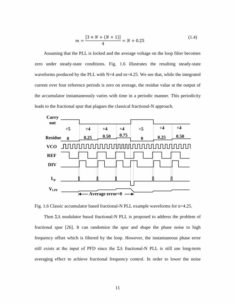
Fig. 1.6 Classic accumulator based fractional-N PLL example waveforms for n=4.25. .. 11
Fig. 2.1 Conventional quadrature VCO with parallel coupling transistors. ..................... 16
Fig. 2.2 Proposed QVCO with optimized capacitive coupling and intrinsic phase shift. 17
Fig. 2.3 Voltage waveforms for different coupling-strength factor m. ............................ 19
Fig. 2.4 Half circuits of differential Colpitts VCOs used to analyze the start-up condition
and resonance frequency: (a) Conventional structure with current tail; (b) ES VCO; (c)
ES VCO with cross-coupled positive feedback at source; (d) ES VCO with cross-coupled
positive feedback at drain. ................................................................................................ 20
Fig. 2.5 Calculation results of (a) Conductance; and (b) Susceptance for different Colpitts
VCOs. Component values used for calculation are as following: C1=0.8 pF, C2=1.2 pF,
L2=1.25 nH, gm=10.3 mS, QL2=15. ................................................................................ 23
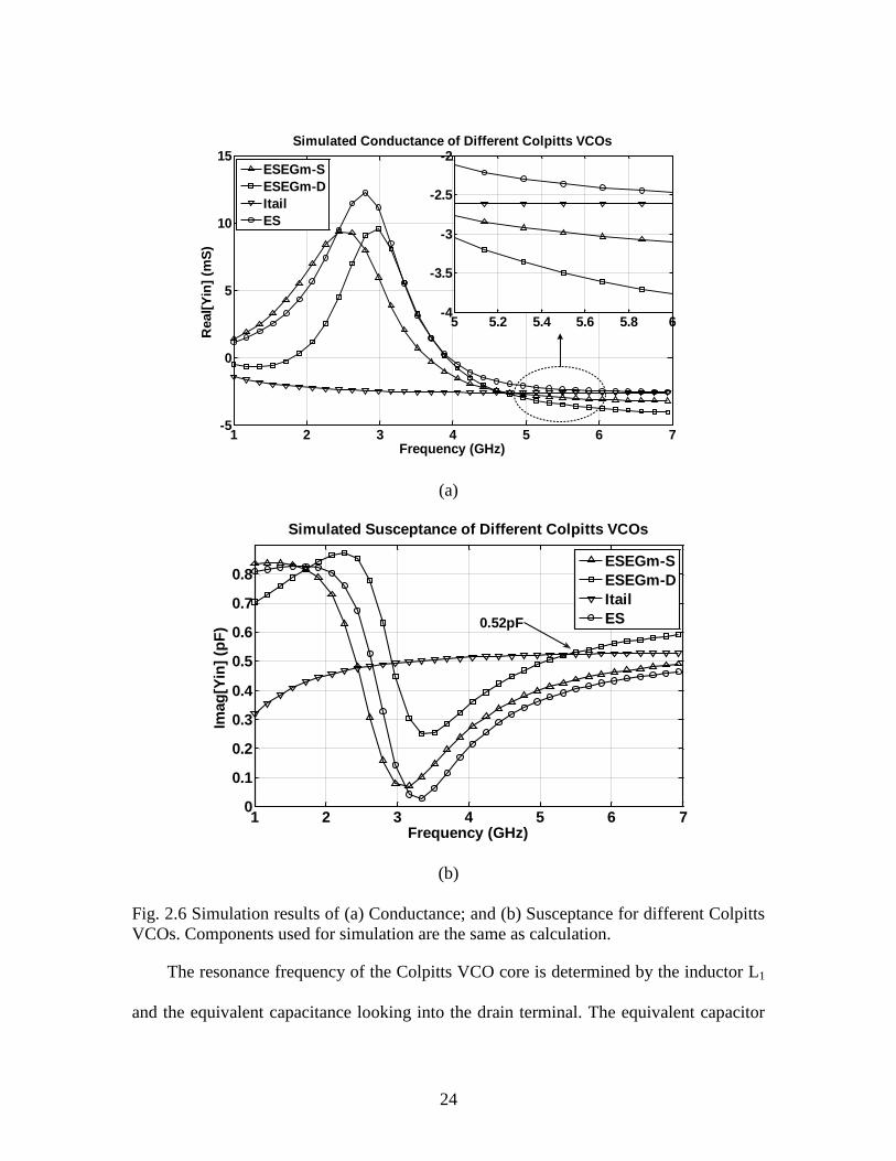
Fig. 2.6 Simulation results of (a) Conductance; and (b) Susceptance for different Colpitts
VCOs. Components used for simulation are the same as calculation. .............................. 24
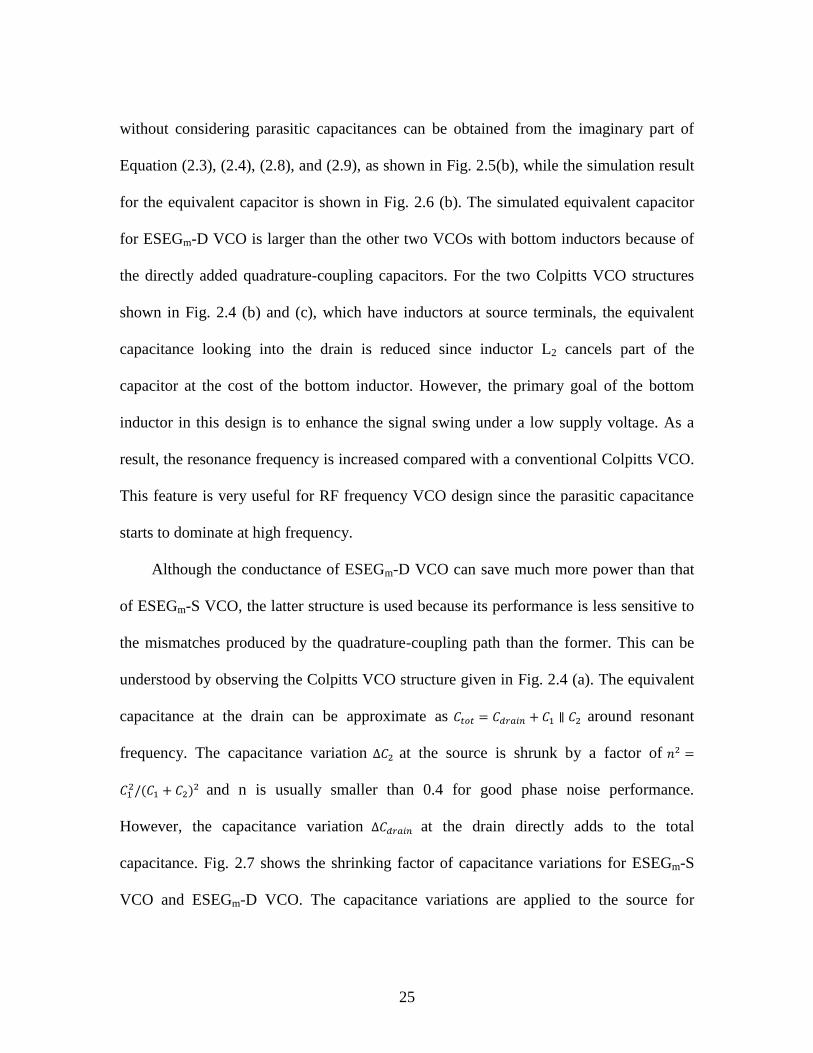
Fig. 2.7 Simulation results of the shrinking factors for ESEGm-D VCO and ESEGm-S
VCO. ................................................................................................................................. 26
Fig. 2.8 Simulation results of CC-QVCO outputs and coupling signals with m=0.4. The
phase difference between the zero-crossing of Iout or Qout and the peak of Igate or Qgate
is about 55º. ....................................................................................................................... 27
Fig. 2.9 ISF and ISFeff for CC-QVCO and SVCO with m=0.4, respectively. .................. 28
Fig. 2.10 Simulation results of phase noise for SVCO and CC-QVCO with m=0.4. ....... 29
x
Fig. 2.11 Simulation results of phase noise improvement and phase error for different
coupling strength factor m with Ctankq=1.01Ctanki. ............................................................ 31
Fig. 2.12 (a) Linear model of quadrature oscillator; and (b) equivalent model of
individual VCO with coupling effects. ............................................................................. 32
Fig. 2.13 (a) CC-QVCO circuit for the derivation of Gc(s); and (b) simplified half-circuit
model for the derivation of Gc(s). The DC bias and varactors (included in C2) are not
shown in the figure and the ground symbols represent ac ground. ................................... 35
Fig. 2.14 Simulation results of phase shift versus analytical formula for quadrature-
coupling transconductance. ............................................................................................... 38
Fig. 2.15 Simulation results of oscillation frequency and phase noise with artificial phase
shift introduced in the coupling path. ............................................................................... 39
Fig. 2.16 Simulation result of output phases with artificial phase shift introduced in the
coupling path (with Ctankq=1.01Ctanki). .............................................................................. 41
Fig. 2.17 Die photo of the implemented QVCO RFIC (1.2×1.2mm2 including pads). .... 42
Fig. 2.18 Measured phase noise of (a) SVCO, and (b) QVCO. ........................................ 42
Fig. 2.19 Measured frequency tuning range and phase noise of QVCO and SVCO. ....... 43
Fig. 2.20 Measured output spectrum for the CC-QVCO. ................................................. 44
Fig. 2.21 Measured output voltage waveforms for the CC-QVCO. ................................. 45
Fig. 3.1 Classic QVCO structure utilizing parallel coupling ............................................ 50
Fig. 3.2 (a) linear model of conventional QVCO, and (b) Phasor diagram illustration of
voltage and current for two phase relationships. .............................................................. 51
Fig. 3.3 QVCO phase noise normalized to SVCO noise for different m and phase delay
(phase noise of SVCO is at 0dB), and γ is assumed to be 2 for short-channel MOS
transistors. ......................................................................................................................... 53
Fig. 3.4 QVCO phase noise without MC devices normalized to QVCO noise with MC
devices for different m and phase delay, and γ is assumed to be 2 for short-channel MOS
transistors. ......................................................................................................................... 54
Fig. 3.5 Proposed CC-QVCO with inherent leading phase shifter for quadrature signal
generation. ......................................................................................................................... 56
Fig. 3.6 Linear model of QVCO including the quadrature-coupling capacitors and cross-
coupling capacitors. .......................................................................................................... 57
Fig. 3.7 Simplified linear model of the proposed QVCO with phase shifter. ................... 58
Fig. 3.8 Phasor diagram of the voltage and current relationships in the proposed CC-
QVCO ............................................................................................................................... 62
Fig. 3.9 Transient waveforms for MRR calculation ......................................................... 63
xi
Fig. 3.10 Minimum gm1,2 required to meet the start-up condition. .................................... 66
Fig. 3.11 Phase noise and phase error with different m and phase shift for CC-QVCO. . 68
Fig. 3.12 Single-phase VCO (SVCO) for comparison ..................................................... 70
Fig. 3.13 Simulated signal amplitudes and phase noise for SVCO. ................................. 70
Fig. 3.14 Simulated signal amplitudes of the CC-QVCO. ................................................ 71
Fig. 3.15 Simulated phase noise and phase error of the proposed QVCO with bias current
for 1.2V and 1.5V supply (1% capacitor mismatch is artificially introduced to the LC
tank). ................................................................................................................................. 72
Fig. 3.16 Proposed QVCO with top-series transistor for quadrature coupling ................. 73
Fig. 3.17 Simulated phase noise and output amplitude of the proposed TS-QVCO ........ 74
Fig. 3.18 TS-QVCO: simulated phase error and FoM for m=2 and m=3 (1% capacitor
mismatch is artificially introduced into the LC tank). ...................................................... 75
Fig. 3.19 CC-QVCO: simulated phase noise and phase error with bias and supply voltage
(1% capacitor mismatch is artificially introduced into the LC tank). ............................... 77
Fig. 3.20 TS-QVCO: simulated phase error and phase noise with bias and supply voltage
(1% capacitor mismatch is artificially introduced into the LC tank). ............................... 77
Fig. 3.21 QVCO phase error and phase noise with temperature (1% capacitor mismatch is
artificially introduced into the LC tank). .......................................................................... 78
Fig. 3.22 Die photos of the implemented CC-QVCO, class-C mode TS-QVCO, and
SVCO. ............................................................................................................................... 80
Fig. 3.23 Auxiliary circuits for phase error measurement: (a) 4 stages of RC poly-phase
filter for IQ baseband signal generation, (b) upconversion mixer. ................................... 80
Fig. 3.24 Measured phase noise performance of the proposed CC-QVCO at 4.7GHz with
a 1.2V power supply and 8.5mA total current. ................................................................. 81
Fig. 3.25 Measured phase noise performance of the proposed TS-QVCO at 4.9GHz with
a 1.2V power supply and 9mA total current. .................................................................... 82
Fig. 3.26 Measured phase noise of the implemented SVCO at 5.35GHz with a 1.2V
power supply and 4.6mA current. ..................................................................................... 83
Fig. 3.27 Measured frequency tuning range of SVCO, CC-QVCO, and TS-QVCO with
1.2V power supply. ........................................................................................................... 83
Fig. 3.28 Measured output spectrum at the output of upconversion mixer where the
frequency is 4.86GHz ....................................................................................................... 84
Fig. 3.29 Measured SBR of CC-QVCO across the tuning range with 1.2V VDD. .......... 85
Fig. 4.1 System diagram of fractional-N PLL with quantization noise cancelling........... 89
Fig. 4.2 ΣΔ modulator structures: (a) MASH1-1, (b) MASH1-1-1, and (c) SSMF.......... 91
xii
Fig. 4.3 Output noise power of ΣΔ modulators with 10MHz sampling clock frequency . 92
Fig. 4.4 PLL model including ΣΔ modulator noise .......................................................... 93
Fig. 4.5 Behavioral model to examine the nonlinearity effect on the quantization noise . 94
Fig. 4.6 Phase noise spectrum of MASH1-1 and MASH1-1-1 with 3% gain mismatch. . 95
Fig. 4.7 Distribution of phase error at the input of PFD for different ΣΔ modulators. ..... 96
Fig. 4.8 Simulated noise improvements by doubling the clock frequency under 3% gain
mismatch. .......................................................................................................................... 97
Fig. 4.9 (a) System diagram of the proposed fractional-N PLL with quantization noise
cancellation technique; (b) PFD circuit. ........................................................................... 99
Fig. 4.10 Pulse control module used to generate PWM signal ......................................... 99
Fig. 4.11 Waveform example for phase error compensation .......................................... 100
Fig. 5.1 System diagram of the proposed PLL system .................................................. 104
Fig. 5.2 Bandgap circuit utilized to generate voltage reference and current reference . 105
Fig. 5.3 Schematic of the proposed VCO with extended tuning range .......................... 108
Fig. 5.4 Divide-by-2 circuit: (a) Circuit schematic and (b) simplified waveforms for
derivation of self-oscillation frequency .......................................................................... 110
Fig. 5.5 Comparison of calculated and simulated self-oscillation frequency of DTC with
R=250Ω, and IB=0.8mA. ............................................................................................... 112
Fig. 5.6 Simulated sensitivity curves of the DTC with R=250 Ω, C=130fF and phase
noise performance with different input signal ................................................................ 113
Fig. 5.7 Circuit schematic of divide-by-2/3 ................................................................... 114
Fig. 5.8 Die photo of the implemented PLL .................................................................. 115
Fig. 5.9 Measured phase noise of the PLL with BW=100kHz, Fref=80MHz ................ 116
Fig. 5.10 Measured VCO frequency tuning range .......................................................... 116
Fig. 5.11 PLL output spectrum ....................................................................................... 117
xiii
List of Tables
Table 2.1: Performance Summary and Comparison of QVCOs with Different Coupling
Techniques ........................................................................................................................ 46
Table 3.1: Performance Summary of the implemented VCO and QVCOs ...................... 86
Table 5.1: Performance Summary of the PLL ................................................................ 117
1
Single chip implementation of wireless transceivers gain popularity as the
fabrication process is gradually developing to smaller feature size since it allows tens of
GHz circuit integration. Among the many building blocks of a radio frequency (RF)
transceiver, clock signal generation is indispensable to provide clean and accurate carrier
for reference. Integer-N or fractional-N phase-locked loop (PLL) frequency synthesizer is
usually utilized to produce such high performance clock signals due to its low power
consumption and accurate frequency synthesis. LC VCO plays a very important role in
providing clean clock signals because of its low power and low noise performance.
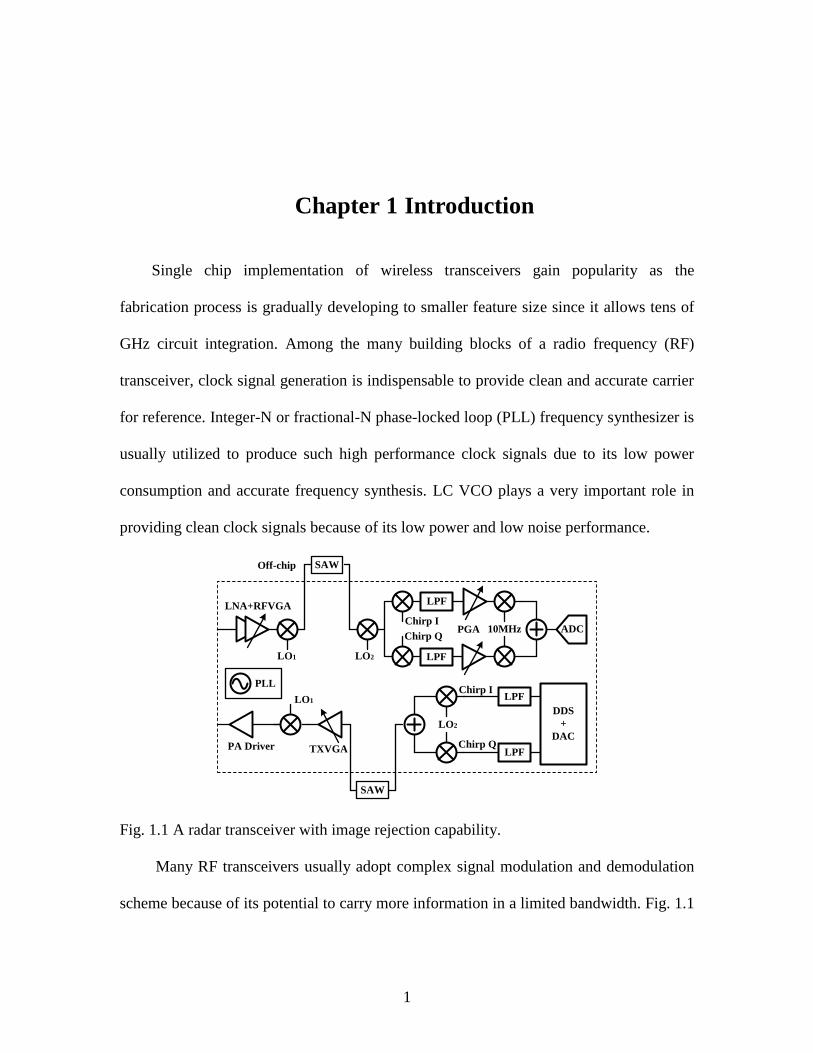
Fig. 1.1 A radar transceiver with image rejection capability.
Many RF transceivers usually adopt complex signal modulation and demodulation
scheme because of its potential to carry more information in a limited bandwidth. Fig. 1.1
SAW
LNA+RFVGALPF
LPF
PGA ADC
LO1
Chirp I10MHz
DDS
+
DAC
LPF
LPF
LO2
Chirp Q
Chirp I
Chirp Q
LO2
LO1
SAW
PLL
PA Driver
Off-chip
TXVGA
Chapter 1 Introduction
2
shows a radar transceiver system that is able to provide gain for the signal at frequency of
fLO+fIF while reject the image signal at frequency of fLO-fIF [1]. It requires a quadrature
local oscillator (LO) signals to upconvert the baseband signal into RF. On the receiver
side, the 10-MHz clock signals are also of quadrature type. Two possible phase
relationships exist for quadrature output, i.e., +90° and -90°; but it is desirable to
maintain the phase relationships in one of the two possible forms since the wrong mode
will amplify the image signal instead of the wanted frequency signal. It is entirely
possible to embed automatic detecting circuit to find the right phase and then select the
right LO signal, but it requires additional circuit. Moreover, the quadrature accuracy
directly affects the signal quality in the transmitted or received signal. Therefore, a
quadrature signal generating mechanism that is able to provide deterministic and accurate
quadrature outputs is essential for image-rejection transceivers.
Several techniques can be employed to produce quadrature signals [2]-[5], i.e., (i) a
voltage-controlled oscillator (VCO) with a doubled frequency followed by a divide-by-
two circuit; (ii) a poly-phase filter; (iii) a quadrature VCO (QVCO). The first method
requires a VCO operating at twice of the desired frequency which consumes more power
because of the additional divide-by-two circuit. The poly-phase filter is a narrow-band
technique with large loss. Compared with the first two techniques, QVCO comprises two
VCO cores coupled with each other and can take advantage of low power consumption.
In addition, its high voltage swing eases the design of the prescaler and the mixer. The
coupling mechanism for a QVCO can be implemented using active devices or passive
components like inductors, transformers, and capacitors. One popular QVCO
3
implementation is coupled with parallel transistors due to its simplicity and low cost of
area [6]. This coupling technique, however, suffers from a trade-off between phase noise
and phase accuracy because the coupling needs to be strong enough to provide decent
phase accuracy, which degrades the quality factor of LC tank and phase noise
performance [5], [7]. Also extra power consumption is required to properly bias the
coupling transistors. In order to improve the phase noise performance, transistors in series
can be placed at the top or bottom of the main amplifying transistors [5], [8]; however,
the parasitic capacitance introduced by the coupling transistors will reduce the frequency
tuning range and the voltage headroom for the signal output is also decreased. Moreover,
extra power consumption is required to maintain the signal amplitude since the coupling
strength required to maintain phase accuracy lowers the signal swing. Another
disadvantage of the QVCO coupling using active devices, especially with parallel
transistors, is the noise degradation resulted from the current noise introduced by the
coupling transistors.
VCO1 VCO2
Quadrature Coupling
O1+ O1- O2+ O2-
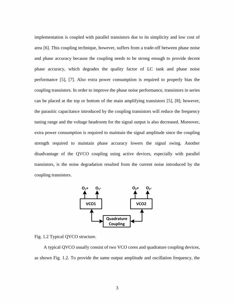
Fig. 1.2 Typical QVCO structure.
A typical QVCO usually consist of two VCO cores and quadrature coupling devices,
as shown Fig. 1.2. To provide the same output amplitude and oscillation frequency, the
4
two VCO cores should have the same structure and device size. Either active device or
passive components is indispensable to form quadrature coupling between the two VCO
cores such that the output can produce quadrature signals. It is obvious that the two
outputs O1 and O2 are symmetric if the quadrature-coupling block is symmetric.
Therefore, the problem of phase ambiguity, meaning that the output phase relations can
be +90° or -90°, may exist in the above QVCO structure. Fortunately this problem can be
addressed by introducing a phase delay in the quadrature-coupling path.
I+ I-
Q+ Q-
Vb1 Vb2
I+ I-
Vb1
Q+ Q-
I+ I-
Vb1
LIO+ LIO-
LQO- LQO+LIS+ LIS-
LQS+ LQS-
(a) (b) (c)
I+ I-
Coupling Circuits
QVCOTail
Vb1
Is
Is Qs Is Qs
Is Qs1 2
3
I+ I-
Q+ Q-
Vb1
(d) (e)
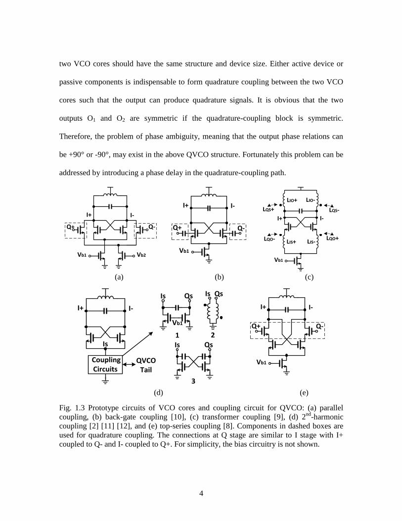
Fig. 1.3 Prototype circuits of VCO cores and coupling circuit for QVCO: (a) parallel
coupling, (b) back-gate coupling [10], (c) transformer coupling [9], (d) 2nd
-harmonic
coupling [2] [11] [12], and (e) top-series coupling [8]. Components in dashed boxes are
used for quadrature coupling. The connections at Q stage are similar to I stage with I+
coupled to Q- and I- coupled to Q+. For simplicity, the bias circuitry is not shown.
5
1.1 Prior Art of QVCO Structures
Fig. 1.3 shows six types of VCO cores used in prior QVCO topologies. Fig. 1.3 (a)
shows the VCO cores used in parallel-coupling QVCO [6]. This structure is simple but
suffers from the noise degradation of the active quadrature-coupling devices. In addition,
the phase delay is limited to the intrinsic delay resulted from the parasitics and thus
cannot successfully avoid bi-modal oscillation.
Back-gate coupling: Fig. 1.3(b) shows the VCO core for QVCO with back-gate
coupling. This technique features the advantages of compact design and low power
consumption by sharing the amplifier transistors with quadrature-coupling path.
However, it requires triple-well CMOS process and is prone to the possibility of forward
biasing the intrinsic bulk-substrate diode. Similar to parallel-coupling technique, it also
suffers from limited phase delay in the quadrature-coupling path.
Transformer coupling: a VCO core used for QVCO with transformer coupling [9] is
shown in Fig. 1.3(c). The noise source for quadrature-coupling has been eliminated in
this structure. The area cost this QVCO does not increase much because the transformer
only occupies a little more metal area. Another advantage of this structure is that the
phase delay in the quadrature-coupling path can be larger than the parallel coupled
QVCO since the quadrature-coupling signal should go through a cascode transistor on top
of before reaching the LC tank, where cascode structure means one transistor is on top of
the other transistor. The remaining problem for such a QVCO design is the difficulty of
constructing a proper transformer model.
Second-harmonic coupling: this technique uses the second harmonic waveform to
6
form the coupling between the two VCO cores. Three coupling examples [2] [11] [12]
with this technique are shown in Fig. 1.3(d). A QVCO design using this technique can be
compact with capacitive coupling. However, the problem of phase ambiguity requires
additional circuit to provide correct directivity.
Top series coupling: Fig. 1.3(e) shows the VCO cores for QVCO with top series
coupling [8] [13]. The noise contribution from the active devices in quadrature-coupling
path can be reduced by utilizing top or bottom series coupling. The active coupling
device is in cascode form and its noise can be degenerated by the bottom transistor. One
advantage of this structure is its capability of rejecting the unwanted oscillation mode.
But the voltage headroom is reduced because of the series transistors. The phase noise
performance is sensitive to bias current and temperature change, which will be
demonstrated by simulation results in Chapter 3.
The resonant frequency of a QVCO varies with the coupling strength and this
feature can be utilized to achieve wide-band frequency tuning range [14] [15]; but the
power consumption is much higher than the classic QVCO structures. As a result, this
structure is not so popular for quadrature generation.
1.2 Analysis of QVCO for Deterministic Quadrature Outputs
As mentioned, the QVCO outputs can be ambiguous if not designed properly,
especially under the influence of PVT variations. Directivity circuits, such as a ring of
transistors [2], can be used to help produce correct output phases. Phase delay is usually
introduced in the quadrature-coupling path to avoid the problem of phase ambiguity, or
7
bi-modal oscillation [2] [16]-[22]. Most phase-shifting circuits achieve a phase delay
much less than the optimum value of 90°; but those phase shifters at least can provide
some safe margin to avoid the problem of bi-modal oscillation.
I+ I-
Q+ Q-
Vb1 Vb2
Vb3 Vb3
I+ I-
Q+ Q-Vb1
Vb2
Vb3 Vb3
Vb2
I+ I-Q+ Q-
Vb1 Vb2
(a) (b) (c)
I+ I-
Q+ Q-Vb1
Vb2
I+ I-
Q+ Q-
Vb1
Cs
I+ I-
Q+d Q-d
Vb1 Vb2
I-d
I+d
(d) (e) (f)
Fig. 1.4 Quadrature phase directivity circuits for QVCO: (a) cascode transistor for
quadrature coupling [16], (b) source coupling [19], (c) resistor based parallel coupling
[21], (d) source degenerated quadrature coupling [20][23][24], (e) capacitive source
degeneration VCO core [17], and (f) RC poly-phase filter for 90 degree phase shift [18].
For simplicity, the bias circuitry is not shown.
Five types of circuit with VCO cores for used for QVCO are shown in Fig. 1.4(a)-
(e). Cascode topology as shown in (a) with a phase delay of 20° is proposed to move the
QVCO operation away from the unstable boundary, therefore giving sufficient phase
margin to avoid bi-modal oscillation [16]. The phase shift is introduced by a pole at high
8
frequency which can be easily found from the following equivalent transconductance
(1.1)
where CP is the parasitic capacitance or artificially introduced capacitor at the source
terminal of the cascode transistor, and gm2 is the transconductance of the cascode
transistor.
The phase shifter shown in Fig. 1.4 (b) and (c) can provide phase delay for stable
operation of QVCO but both suffer from noise degradation. The quality factor of the LC
tank in (b) is decreased because the source input impedance of 1/gm will load the resonant
tank; while the series resistors in the quadrature-coupling path add to the output noise.
Another type of phase shifter uses RC source degeneration network to provide phase
delay [20] [23] [24], as shown in Fig. 1.4(d). It is advantageous over cascode phase
shifter because it does not suffer from the problem of degraded voltage headroom and can
be embedded into the main VCO cores as shown in (e) [17]. The effective
transconductance of the quadrature-coupling circuits for (d) and (e) are
( )
(1.2)
(1.3)
Usually, the phase shifters mentioned above only achieves a phase shift around 45°
in practical QVCO design and it is still far away from the optimum condition of 90°.
Mirzaei [18] suggested RC poly phase shifter to produce the 90° phase shift for optimum
operation of QVCO as shown in Fig. 1.4(f). A phase shift of 72° has been achieved due
9
to the load effect in the real implementation according to the publication. However, the
quality factor of the LC tank can be easily degraded by the RC poly-phase filter,
especially when a high quality tank is required.
1.3 Phase-Locked Loop Frequency Synthesizer
PLL circuits are widely used to generate a precise frequency signal from a very high
precision reference signal. It has wide application in wired and wireless communications
systems to provide accurate carrier that is phase aligned with the incoming high-precision
reference clock signal. The VCO signal is divided and compared with the high-precision
reference by the phase frequency detector (PFD). Then the error signal is fed into charge
pump to transform the phase error into current pulses. The pulses are filtered by the loop
filter and then the filtered voltage is used to control the VCO to stabilize its phase and
frequency variations. The negative feedback mechanism results in the generation of a
tunable and stable output signal at the desired frequency.
Two types of PLL structures with negative feedback loop, integer-N and fractional-
N, have been widely used for frequency synthesis. Integer-N PLL, as shown in Fig. 1.5
(a), provide an output frequency equals to N times the reference frequency whereas N is
the divider ratio. However, this architecture limits the frequency resolution to the PFD
comparison frequency.
Another architecture named as fractional-N PLL has become increasingly popular
since its invention because it can achieve fine frequency resolution with larger loop
bandwidth than integer-N PLL. Unlike integer-N PLL, fractional-N PLL allows a
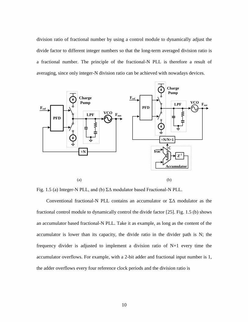
10
division ratio of fractional number by using a control module to dynamically adjust the
divide factor to different integer numbers so that the long-term averaged division ratio is
a fractional number. The principle of the fractional-N PLL is therefore a result of
averaging, since only integer-N division ratio can be achieved with nowadays devices.
VCOFout
PFD
Fref
÷N
Charge
Pump
LPF
VCOFout
PFD
Fref
÷N/N+1
Charge
Pump
LPF
Z-1
Ad
derfrac
Accumulator
C
(a) (b)
Fig. 1.5 (a) Integer-N PLL, and (b) ΣΔ modulator based Fractional-N PLL.
Conventional fractional-N PLL contains an accumulator or ΣΔ modulator as the
fractional control module to dynamically control the divide factor [25]. Fig. 1.5 (b) shows
an accumulator based fractional-N PLL. Take it as example, as long as the content of the
accumulator is lower than its capacity, the divide ratio in the divider path is N; the
frequency divider is adjusted to implement a division ratio of N+1 every time the
accumulator overflows. For example, with a 2-bit adder and fractional input number is 1,
the adder overflows every four reference clock periods and the division ratio is
11
[ ( )]
(1.4)
Assuming that the PLL is locked and the average voltage on the loop filter becomes
zero under steady-state conditions. Fig. 1.6 illustrates the resulting steady-state
waveforms produced by the PLL with N=4 and m=4.25. We see that, while the integrated
current over four reference periods is zero on average, the residue value at the output of
the accumulator instantaneously varies with time in a periodic manner. This periodicity
leads to the fractional spur that plagues the classical fractional-N approach.
0 0.25 0.50 0.750.25 0.50
0
÷4 ÷4 ÷4 ÷5÷5 ÷4 ÷4
Carry
out
Residue
VCO
REF
DIV
Icp
VLPF
Average error=0
Fig. 1.6 Classic accumulator based fractional-N PLL example waveforms for n=4.25.
Then ΣΔ modulator based fractional-N PLL is proposed to address the problem of
fractional spur [26]. It can randomize the spur and shape the phase noise to high
frequency offset which is filtered by the loop. However, the instantaneous phase error
still exists at the input of PFD since the ΣΔ fractional-N PLL is still use long-term
averaging effect to achieve fractional frequency control. In order to lower the noise
12
degradation caused by the ΣΔ modulator, a phase error compensation mechanism is
therefore indispensable to achieve the goal of wide-bandwidth modulation in fractional-N
PLL.
In attempt to reduce the noise caused by ΣΔ modulators, a compensating pulse-
amplitude-modulated (PAM) current can be injected into the loop filter and efficiently
compensated the phase error. The current is generated from a current digital-to-analog
converter (DAC) with fixed pulse width. This technique can be applied to accumulator
based and ΣΔ modulator based fractional-N PLL [25] [27]. The compensation technique
based on PAM requires high-precision DAC current generator to completely compensate
the phase error. It needs more complicate control technique like dynamical element
match (DEM) to reduce the mismatch of DAC current generator. PFD/DAC can be
embedded to improve the compensating accuracy [25]; however, it can be only applied to
first order ΣΔ modulator or modulators with a phase error less than one VCO period.
Therefore, it is desirable to develop a PLL system that is able to suppress the quantization
noise caused by high order ΣΔ modulator.
1.4 Outline and Contribution
This dissertation focuses on the topic of capacitive-coupling quadrature VCO, with a
particular on phase noise reduction and elimination of phase ambiguity. Chapter 2 aims to
develop a differential Colpitts QVCO with enhanced swing technique and capacitive
quadrature-coupling mechanism for low phase noise performance under 0.6-V power
supply. Silicon verification results are also given to demonstrate the proposed technique.
13
In chapter 3, quadrature-coupling technique, combined with inherent phase shifter,
is applied to classic NMOS VCO with current tail for quadrature generation. The
proposed structure demonstrates excellent phase noise and phase error performance over
a wide frequency range. Implementation and measurement results are given to show the
robustness of the proposed QVCO structure.
Chapter 4 explores several quantization reduction techniques for fractional-N PLL.
Nonlinearity analysis of four types of popular ΣΔ modulator structures and simple noise
reduction technique have been discussed. A concept for high-order ΣΔ modulator noise
cancellation is proposed for fractional-N PLL.
Chapter 5 describes a wideband integer-N PLL with 4.8-6.8GHz output frequency
range. The design details about the VCO, multi-modulus divider, and bandgap reference
are explained. A power optimization methodology is developed for divider design.
Chapter 6 summarizes this dissertation and suggests future research topics.
14
2.1 Introduction
Phase noise and phase accuracy are two essential specifications for quadrature signal
generation since the two aspects directly affect the quality of the received or transmitted
signal in a wireless communication system. The ever-growing demand for chip-level
integration of multi-band transceiver continues imposing tighter phase noise performance
specifications for radio-frequency (RF) carrier generation. Quadrature signals with phase
accuracy and no phase ambiguity are critical for image-rejection transceivers since they
directly affect the polarity and the outcome of the complex mixers. Phase error existed in
the quadrature signals will add to the error of a baseband signal and deteriorate the bit
error rate (BER) of a communication system. Thus, a high performance quadrature signal
generation technique with both low noise and decent phase accuracy is highly desirable
for complex signal modulation and demodulation.
To eliminate noise degradation introduced by the coupling mechanism, noiseless
components such as transformer, inductor, and capacitor can be used for coupling. A
QVCO with transformer coupling which is based on the technique of super-harmonic
coupling [2] shows good phase noise performance with the expense of inductor area. An
Chapter 2 A 0.6-V Low-Phase Noise CC-QVCO with
Enhanced Swing
15
energy-circulating QVCO with inductive coupling can achieve even much better phase
noise performance than the single-phase VCO of the same kind [28], yet it comes at the
cost of additional area of two inductors. In order to reduce the area of a coupling
transformer, the secondary coupling tank can share the tank area with the resonant tank
and it can achieve a decent figure-of-merit (FoM) [9]. However, transformer models are
either not accurate or not available in most commercial CMOS technology and it requires
extra effort to develop an accurate transformer model. Therefore, QVCO with capacitive
coupling techniques [11] [29] [30] have been developed to simplify the circuit design
with good noise performance and small area.
Various QVCO coupling mechanisms have been developed in search of improved
phase noise performance, yet another important aspect of the QVCO design, the phase
ambiguity, is often overlooked. The understanding of the phase ambiguity and the
stability is critical since a typical QVCO may operate at either one of its two stable
modes with different phase relationships. Each stable mode corresponds to +90º or -90º
phase relationship between the two outputs of the QVCO. However, quadrature signals
with deterministic phase relationship are often required for proper image rejection in RF
receivers [24]. The phenomenon of the bimodal oscillation has been observed and phase
shifter in the coupling path can help solving this problem [16]-[18]. Theoretical analysis
and experimental results prove that the phase shift of 90º introduced in the quadrature-
coupling path provides optimum phase noise performance and minimum phase error
arising from mismatch between two VCO cores [18]. However, the phase shift of 90º has
16
to be implemented with poly-phase shifters [18], or additional active devices stages [19],
or source degenerated phase shifter [20] for QVCO using parallel coupling transistors.
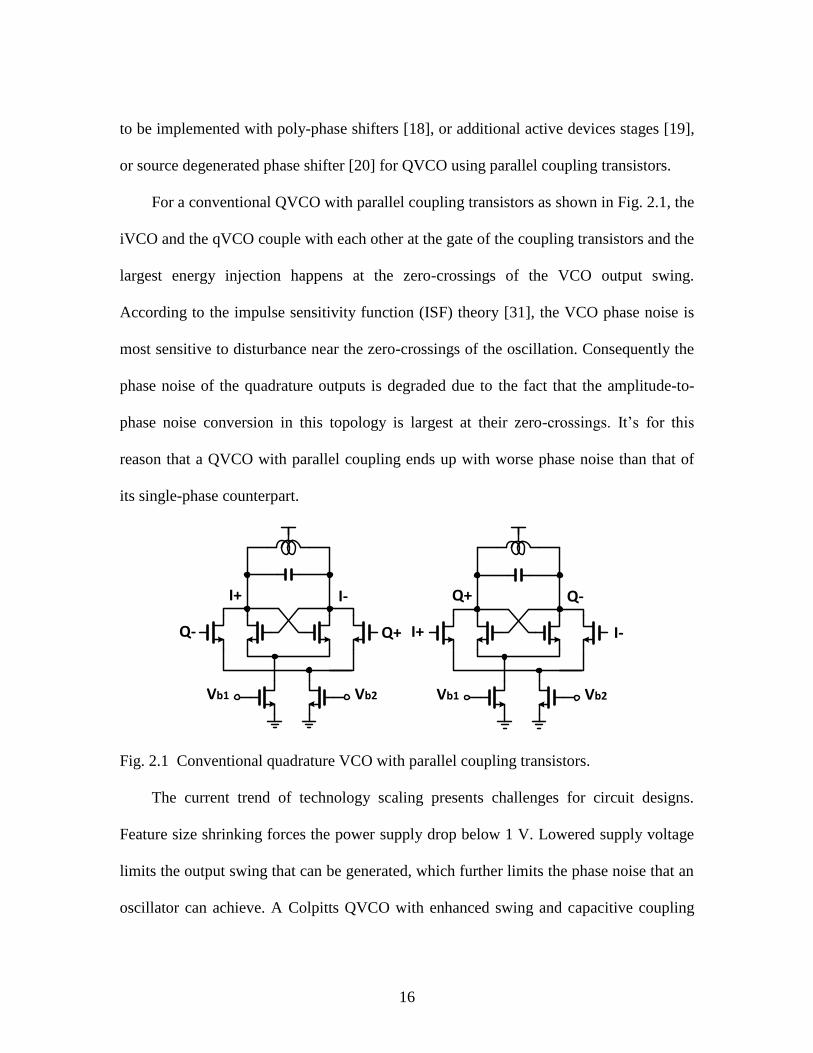
For a conventional QVCO with parallel coupling transistors as shown in Fig. 2.1, the
iVCO and the qVCO couple with each other at the gate of the coupling transistors and the
largest energy injection happens at the zero-crossings of the VCO output swing.
According to the impulse sensitivity function (ISF) theory [31], the VCO phase noise is
most sensitive to disturbance near the zero-crossings of the oscillation. Consequently the
phase noise of the quadrature outputs is degraded due to the fact that the amplitude-to-
phase noise conversion in this topology is largest at their zero-crossings. It’s for this
reason that a QVCO with parallel coupling ends up with worse phase noise than that of
its single-phase counterpart.
I+ I-
Q- Q+
Vb1
Q+ Q-
I+ I-
Vb2 Vb1 Vb2
Fig. 2.1 Conventional quadrature VCO with parallel coupling transistors.
The current trend of technology scaling presents challenges for circuit designs.
Feature size shrinking forces the power supply drop below 1 V. Lowered supply voltage
limits the output swing that can be generated, which further limits the phase noise that an
oscillator can achieve. A Colpitts QVCO with enhanced swing and capacitive coupling
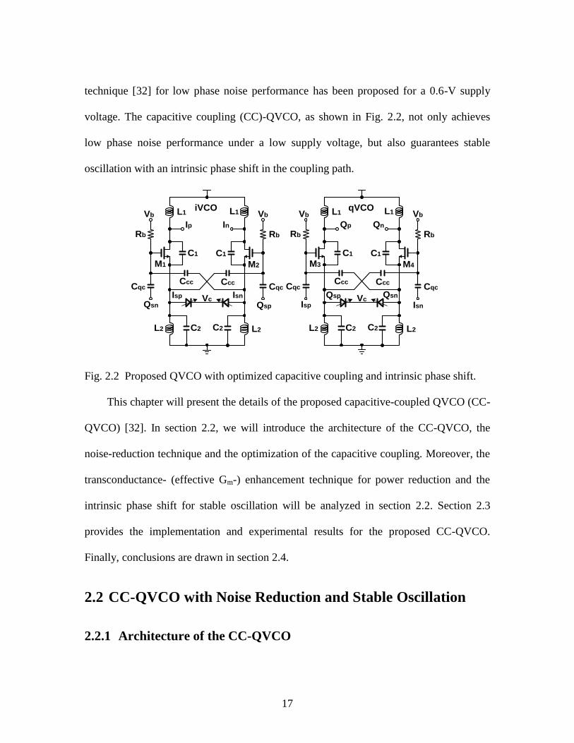
17
technique [32] for low phase noise performance has been proposed for a 0.6-V supply
voltage. The capacitive coupling (CC)-QVCO, as shown in Fig. 2.2, not only achieves
low phase noise performance under a low supply voltage, but also guarantees stable
oscillation with an intrinsic phase shift in the coupling path.
C1
C2
C1
Vc
L2 L2
L1 L1
Ip In
Isp Isn
Vb Vb
Qsn Qsp
Rb Rb
CqcCqcCcc Ccc
M1 M2
C1 C1
Vc
L2 L2
L1 L1
Qp Qn
Qsp Qsn
Vb Vb
Isp Isn
Rb Rb
CqcCqcCcc Ccc
M3 M4
iVCO qVCO
C2 C2 C2
Fig. 2.2 Proposed QVCO with optimized capacitive coupling and intrinsic phase shift.
This chapter will present the details of the proposed capacitive-coupled QVCO (CC-
QVCO) [32]. In section 2.2, we will introduce the architecture of the CC-QVCO, the
noise-reduction technique and the optimization of the capacitive coupling. Moreover, the
transconductance- (effective Gm-) enhancement technique for power reduction and the
intrinsic phase shift for stable oscillation will be analyzed in section 2.2. Section 2.3
provides the implementation and experimental results for the proposed CC-QVCO.
Finally, conclusions are drawn in section 2.4.
2.2 CC-QVCO with Noise Reduction and Stable Oscillation
2.2.1 Architecture of the CC-QVCO
18
As shown in Fig. 2.2, instead of using noisy transistors for quadrature signal
coupling, capacitive coupling is employed to improve the phase noise performance of the
QVCO. To achieve large output swing required for good phase noise performance under
a low supply voltage around 0.6 V, an enhance-swing (ES) Colpitts VCO structure
similar to [33] is adopted. Different from simple ES Colpitts VCO, Gm- enhancement
technique is employed using the cross-coupled capacitors Ccc to reduce the power
consumption. The proposed CC-QVCO is composed of two such Gm-enhanced VCO
cores and four quadrature-coupling capacitors Cqc. The coupling-strength factor m
between the iVCO and qVCO is defined as
(2.1)
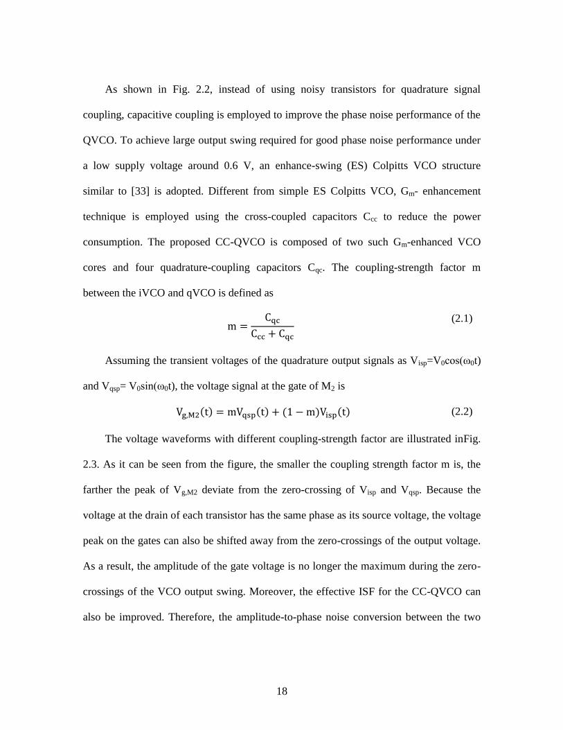
Assuming the transient voltages of the quadrature output signals as Visp=V0cos(ω0t)
and Vqsp= V0sin(ω0t), the voltage signal at the gate of M2 is
( ) ( ) ( ) ( ) (2.2)
The voltage waveforms with different coupling-strength factor are illustrated inFig.
2.3. As it can be seen from the figure, the smaller the coupling strength factor m is, the
farther the peak of Vg,M2 deviate from the zero-crossing of Visp and Vqsp. Because the
voltage at the drain of each transistor has the same phase as its source voltage, the voltage
peak on the gates can also be shifted away from the zero-crossings of the output voltage.
As a result, the amplitude of the gate voltage is no longer the maximum during the zero-
crossings of the VCO output swing. Moreover, the effective ISF for the CC-QVCO can
also be improved. Therefore, the amplitude-to-phase noise conversion between the two
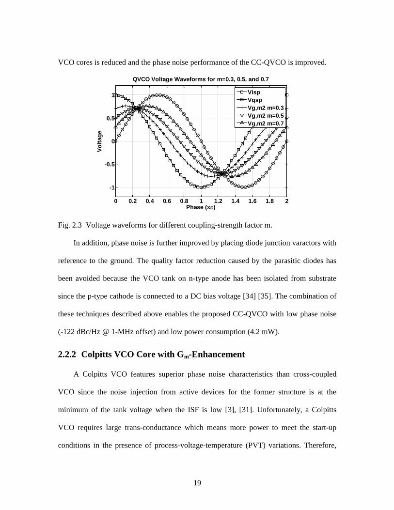
19
VCO cores is reduced and the phase noise performance of the CC-QVCO is improved.
Fig. 2.3 Voltage waveforms for different coupling-strength factor m.
In addition, phase noise is further improved by placing diode junction varactors with
reference to the ground. The quality factor reduction caused by the parasitic diodes has
been avoided because the VCO tank on n-type anode has been isolated from substrate
since the p-type cathode is connected to a DC bias voltage [34] [35]. The combination of
these techniques described above enables the proposed CC-QVCO with low phase noise
(-122 dBc/Hz @ 1-MHz offset) and low power consumption (4.2 mW).
2.2.2 Colpitts VCO Core with Gm-Enhancement
A Colpitts VCO features superior phase noise characteristics than cross-coupled
VCO since the noise injection from active devices for the former structure is at the
minimum of the tank voltage when the ISF is low [3], [31]. Unfortunately, a Colpitts
VCO requires large trans-conductance which means more power to meet the start-up
conditions in the presence of process-voltage-temperature (PVT) variations. Therefore,
0 0.2 0.4 0.6 0.8 1 1.2 1.4 1.6 1.8 2
-1
-0.5
0
0.5
1
Phase (x)
Vo
ltag
e
QVCO Voltage Waveforms for m=0.3, 0.5, and 0.7
Visp
Vqsp
Vg,m2 m=0.3
Vg,m2 m=0.5
Vg,m2 m=0.7
20
high power dissipation is necessary to ensure reliable start-up.
Fig. 2.4 shows the half circuits of different Colpitts VCO topologies. The derivation
of the small-signal admittance for Colpitts VCO with current tail as shown in Fig. 4(a) is
straightforward and can be written as
( )
(2.3)
where the gm is the transconductance of M1. The admittance of an ES-Colpitts VCO
shown in Fig. 2.4(b) with tank 2 to enhance the signal swing is given by
( )
( )
(2.4)
(2.5)
C1
IB
Vb
Rb
M1
C2
Ix
Vx
C1
L2
Vb
Rb
M1
C2
Tank 2
Ix
Vx
C1
L2
Vb
Rb
Ccc
M1
C2
Tank 2
Cqc
Vs
-Vs
Ix
Vx
C1
L2
Vb
Rb
Ccc
M1
C2
Tank 2
-Vx
Cqc
Ix
Vx
(a) (b) (c) (d)
Fig. 2.4 Half circuits of differential Colpitts VCOs used to analyze the start-up condition
and resonance frequency: (a) Conventional structure with current tail; (b) ES VCO; (c)
ES VCO with cross-coupled positive feedback at source; (d) ES VCO with cross-coupled
positive feedback at drain.
Equation (2.4) is based on ideal lossless inductor L2, i.e. RP2=∞. Shown in Fig. 2.4
(c) and (d) are other two Colpitts VCO structures with Gm-enhancement. ES VCO of Fig.
21
2.4 (c) places the cross-coupled capacitor at the source. The admittance looking into the
half-circuit can be derived with the Kirchhoff’s circuit laws (KCL). The voltage at the
drain can be expressed as
( )
(2.6)
The admittance for the ES VCO with Gm-enhancement placed at source (ESEGm-S)
is defined as
( )
(2.7)
where the gm is the transconductance of M1. By assuming an ideal lossless inductor L2,
the admittance for ESEGm-S VCO can be rewritten as
(
)
( ) ( )
(2.8)
Similarly, the admittance for ESEGm-D VCO as shown in Fig. 4(d) can be derived
as
( ) ( )
[ ( ) ](
)
( )
(2.9)
The real parts of those equations represent the negative transconductance required to
start the oscillator. The larger the absolute value of the transconductance is, the smaller
the power consumption is required for start-up. Oscillators will fail to start oscillation
when the negative admittance cannot compensate the tank loss. The real admittances for
the four VCO topologies are expressed as follows.
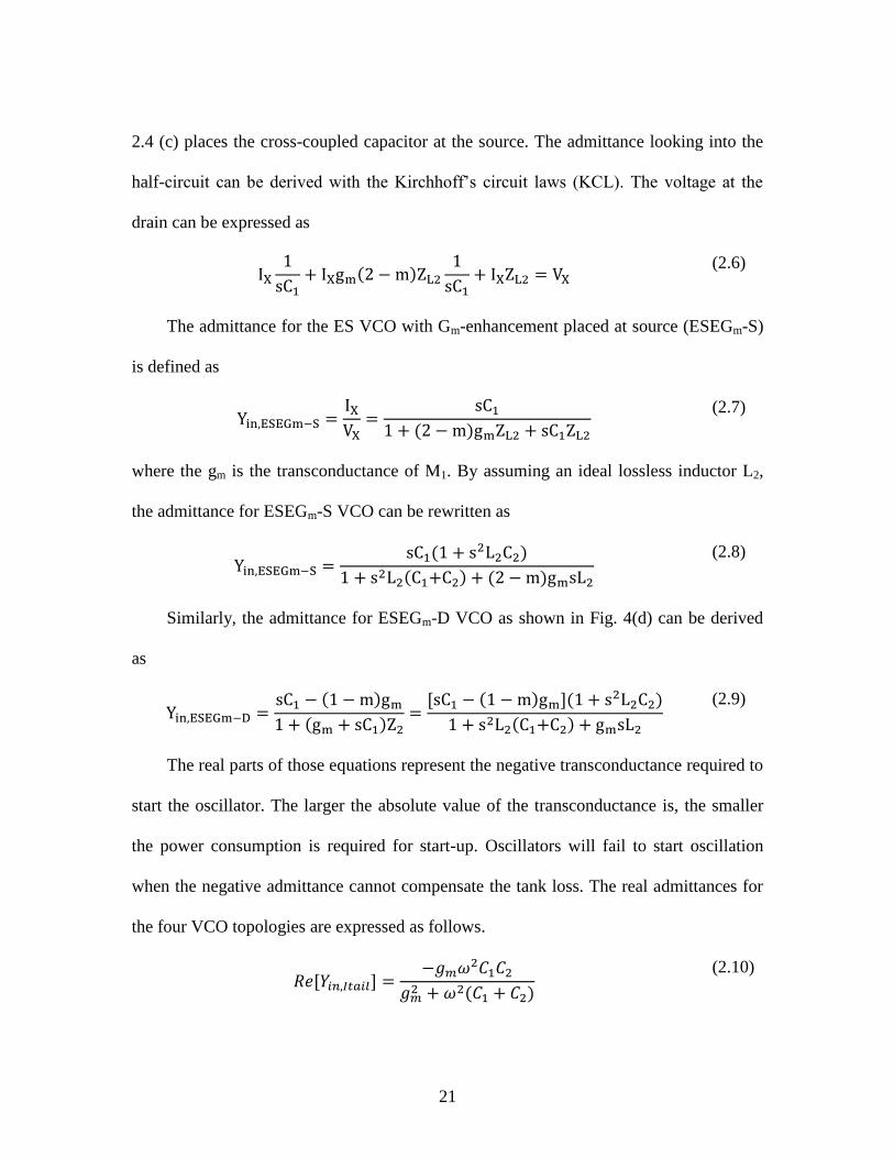
[ ]
( )
(2.10)
22
[ ]
( )
[ ( )] ( )
(2.11)
[ ] ( )
( )
[ ( )] [( ) ]
(2.12)
[ ]
( )
( )[
( )]
[ ( )] ( )
(2.13)
Fig. 2.5 (a) shows the calculated real admittances of the four VCO structures. As
shown in the frequency range of 5~6 GHz, the conductance of ESEGm-S VCO is about
1.5 times that of ES VCO and thus relaxes the start-up requirement. Compared with
conventional Colpitts VCO with ideal current tail, the improvement at f=5.5 GHz is about
35%. Therefore, the power consumption is reduced and improved FoM can be achieved.
The improvement has been verified through simulation and the simulated admittances are
shown in Fig. 2.6. Although the simulated conductance improvement is smaller than the
calculation result, the Colpitts VCOs with Gm- enhancement as shown in Fig. 2.4 (c) and
(d) still achieve lower power consumption than the other two structures. The
discrepancies between the Fig. 2.5 and Fig. 2.6 are caused not only by using simplified
small-signal transistor models with first-order approximation, but also by neglecting Cqc,
Ccc, and other parasitic capacitances for deriving the analytic expressions. However, Fig.
2.5 gives first-order approximation of the admittances. The magnitude of negative Gm
decreases when frequency is reduced, i.e., it becomes more difficult for the VCOs to meet
the start-up condition as frequency decreases. After a certain frequency value, the Gm
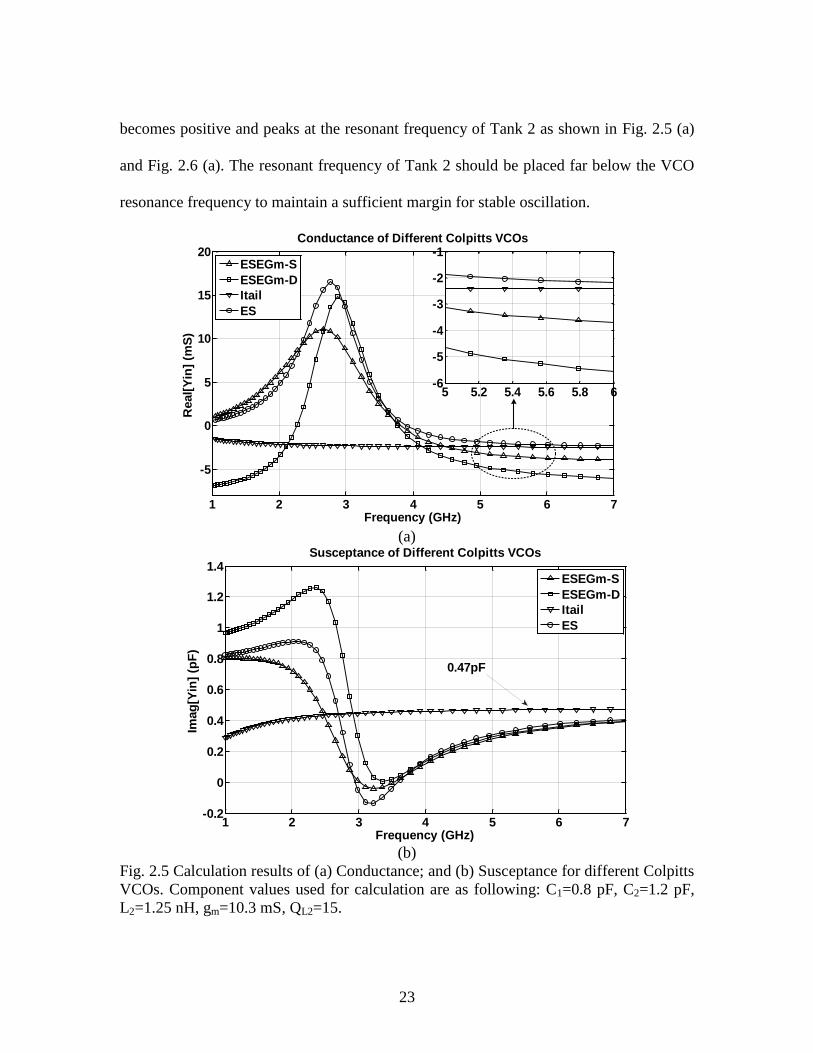
23
becomes positive and peaks at the resonant frequency of Tank 2 as shown in Fig. 2.5 (a)
and Fig. 2.6 (a). The resonant frequency of Tank 2 should be placed far below the VCO
resonance frequency to maintain a sufficient margin for stable oscillation.
1 2 3 4 5 6 7
-5
0
5
10
15
20
Frequency (GHz)
Real[
Yin
] (m
S)
Conductance of Different Colpitts VCOs
ESEGm-S
ESEGm-D
Itail
ES
5 5.2 5.4 5.6 5.8 6-6
-5
-4
-3
-2
-1
(a)
(b)
Fig. 2.5 Calculation results of (a) Conductance; and (b) Susceptance for different Colpitts
VCOs. Component values used for calculation are as following: C1=0.8 pF, C2=1.2 pF,
L2=1.25 nH, gm=10.3 mS, QL2=15.
1 2 3 4 5 6 7-0.2
0
0.2
0.4
0.6
0.8
1
1.2
1.4
Frequency (GHz)
Imag
[Yin
] (p
F)
Susceptance of Different Colpitts VCOs
ESEGm-S
ESEGm-D
Itail
ES
0.47pF
24
1 2 3 4 5 6 7-5
0
5
10
15
Frequency (GHz)
Real[
Yin
] (m
S)
Simulated Conductance of Different Colpitts VCOs
ESEGm-S
ESEGm-D
Itail
ES
5 5.2 5.4 5.6 5.8 6-4
-3.5
-3
-2.5
-2
(a)
(b)
Fig. 2.6 Simulation results of (a) Conductance; and (b) Susceptance for different Colpitts
VCOs. Components used for simulation are the same as calculation.
The resonance frequency of the Colpitts VCO core is determined by the inductor L1
and the equivalent capacitance looking into the drain terminal. The equivalent capacitor
1 2 3 4 5 6 70
0.1
0.2
0.3
0.4
0.5
0.6
0.7
0.8
Frequency (GHz)
Imag
[Yin
] (p
F)
Simulated Susceptance of Different Colpitts VCOs
ESEGm-S
ESEGm-D
Itail
ES0.52pF
25
without considering parasitic capacitances can be obtained from the imaginary part of
Equation (2.3), (2.4), (2.8), and (2.9), as shown in Fig. 2.5(b), while the simulation result
for the equivalent capacitor is shown in Fig. 2.6 (b). The simulated equivalent capacitor
for ESEGm-D VCO is larger than the other two VCOs with bottom inductors because of
the directly added quadrature-coupling capacitors. For the two Colpitts VCO structures
shown in Fig. 2.4 (b) and (c), which have inductors at source terminals, the equivalent
capacitance looking into the drain is reduced since inductor L2 cancels part of the
capacitor at the cost of the bottom inductor. However, the primary goal of the bottom
inductor in this design is to enhance the signal swing under a low supply voltage. As a
result, the resonance frequency is increased compared with a conventional Colpitts VCO.
This feature is very useful for RF frequency VCO design since the parasitic capacitance
starts to dominate at high frequency.
Although the conductance of ESEGm-D VCO can save much more power than that
of ESEGm-S VCO, the latter structure is used because its performance is less sensitive to
the mismatches produced by the quadrature-coupling path than the former. This can be
understood by observing the Colpitts VCO structure given in Fig. 2.4 (a). The equivalent
capacitance at the drain can be approximate as around resonant
frequency. The capacitance variation at the source is shrunk by a factor of
( )
and n is usually smaller than 0.4 for good phase noise performance.
However, the capacitance variation at the drain directly adds to the total
capacitance. Fig. 2.7 shows the shrinking factor of capacitance variations for ESEGm-S
VCO and ESEGm-D VCO. The capacitance variations are applied to the source for
26
ESEGm-S VCO and the drain for ESEGm-D VCO. From the Fig. 2.7, it is known that the
shrinking factor for the ESEGm-S VCO is about one fourth of that of the ESEGm-D VCO
around the target frequency. Therefore, the ESEGm-S VCO suffers less from the
mismatch in the quadrature-coupling path than the ESEGm-D VCO.
Fig. 2.7 Simulation results of the shrinking factors for ESEGm-D VCO and ESEGm-S
VCO.
2.2.3 Noise Reduction for the CC-QVCO
Ideally the phase noise of a QVCO can be reduced by 3 dB compared to a single-
phase VCO that draw half of the current of the QVCO, and a phase noise normalized to
the power consumption would be the same as its single phase counterpart [8]. This
assumption does not take into account of various effects that have impact on the phase
noise performance, such as additional noise generated by the coupling devices and the
reduction of effective quality factor of the LC tanks. On the other hand, the coupled
signal is usually at its maximum when the QVCO is most susceptible to noise, i.e., when
1 2 3 4 5 6 7-0.5
0
0.5
1
1.5
Frequency (GHz)
Gain
Simulated Shrinking Factor for Capacitance Variations
ESEGm-S
ESEGm-D
0.24
27
the two VCO cores inject noise to each other during the zero-crossing point of their
output swings. Due to both the additional noise introduced by coupling transistors and
noise injection around the most sensitive time of output signals, the phase noise
normalized to power consumption of the QVCO based on series or parallel coupling [5]-
[8] can only be close, but not as good as that of its single-phase counterpart.
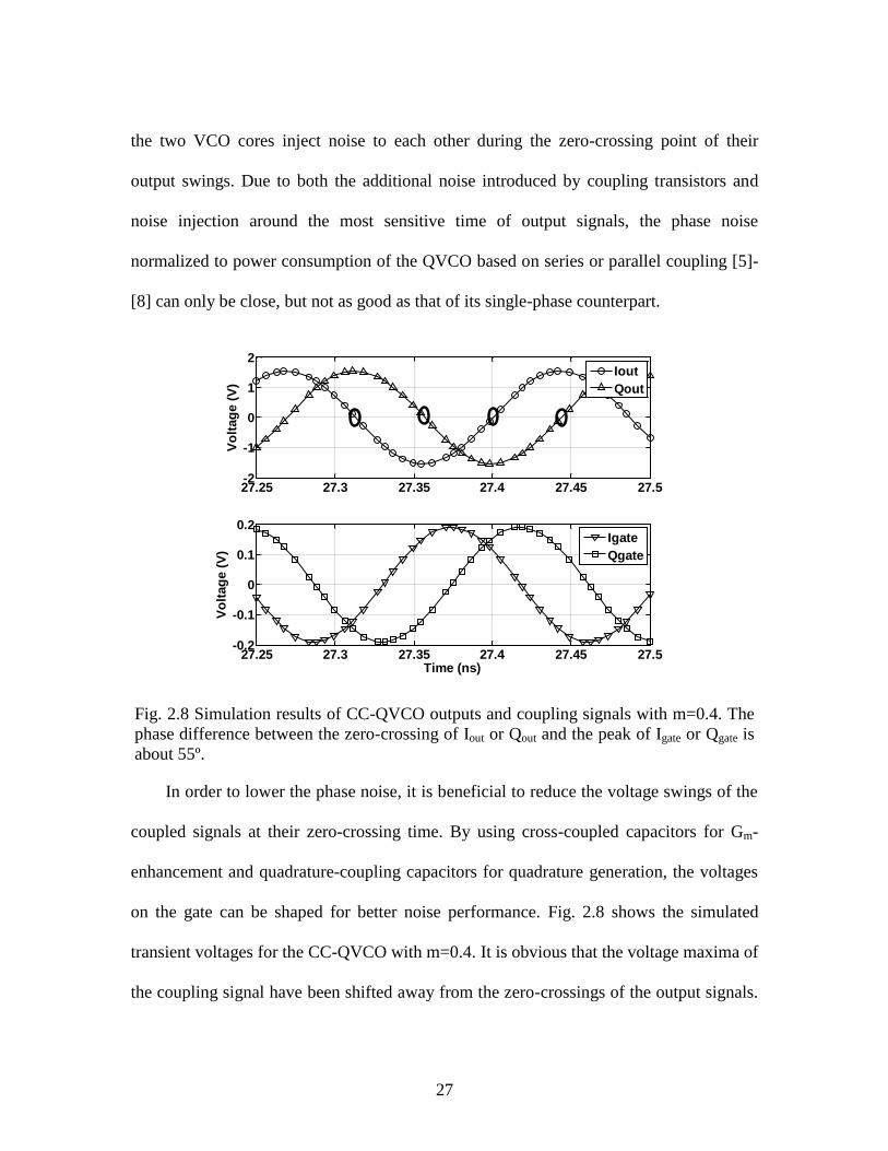
Fig. 2.8 Simulation results of CC-QVCO outputs and coupling signals with m=0.4. The
phase difference between the zero-crossing of Iout or Qout and the peak of Igate or Qgate is
about 55º.
In order to lower the phase noise, it is beneficial to reduce the voltage swings of the
coupled signals at their zero-crossing time. By using cross-coupled capacitors for Gm-
enhancement and quadrature-coupling capacitors for quadrature generation, the voltages
on the gate can be shaped for better noise performance. Fig. 2.8 shows the simulated
transient voltages for the CC-QVCO with m=0.4. It is obvious that the voltage maxima of
the coupling signal have been shifted away from the zero-crossings of the output signals.
27.25 27.3 27.35 27.4 27.45 27.5-2
-1
0
1
2
Vo
ltag
e (
V)
Iout
Qout
27.25 27.3 27.35 27.4 27.45 27.5-0.2
-0.1
0
0.1
0.2
Time (ns)
Vo
ltag
e (
V)
Igate
Qgate
28
As a result, the amplitude-to-phase noise conversion between the two VCO cores is
reduced and the phase noise performance of the CC-QVCO is improved beyond what can
be achieved by its single-phase counterpart.
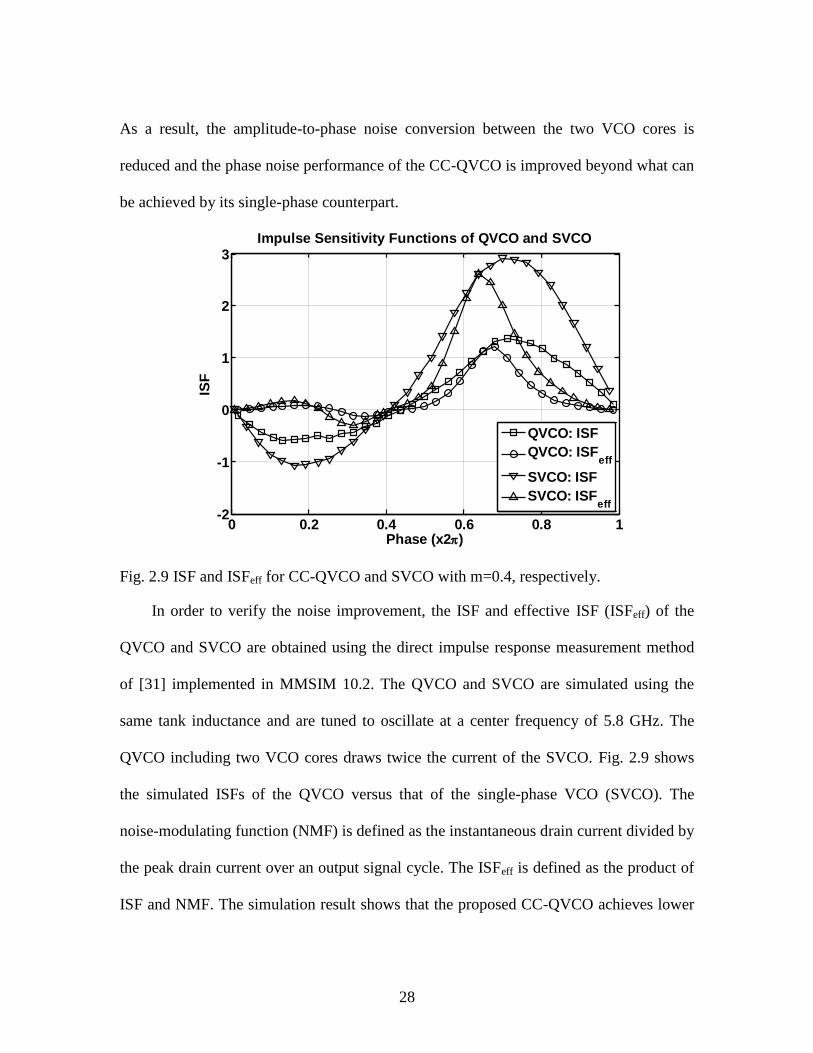
Fig. 2.9 ISF and ISFeff for CC-QVCO and SVCO with m=0.4, respectively.
In order to verify the noise improvement, the ISF and effective ISF (ISFeff) of the
QVCO and SVCO are obtained using the direct impulse response measurement method
of [31] implemented in MMSIM 10.2. The QVCO and SVCO are simulated using the
same tank inductance and are tuned to oscillate at a center frequency of 5.8 GHz. The
QVCO including two VCO cores draws twice the current of the SVCO. Fig. 2.9 shows
the simulated ISFs of the QVCO versus that of the single-phase VCO (SVCO). The
noise-modulating function (NMF) is defined as the instantaneous drain current divided by
the peak drain current over an output signal cycle. The ISFeff is defined as the product of
ISF and NMF. The simulation result shows that the proposed CC-QVCO achieves lower
0 0.2 0.4 0.6 0.8 1-2
-1
0
1
2
3
Phase (x2)
ISF
Impulse Sensitivity Functions of QVCO and SVCO
QVCO: ISF
QVCO: ISFeff
SVCO: ISF
SVCO: ISFeff
29
ISF and effective ISFeff than its SVCO core. The corresponding coefficient ratio of c0svco
to c0qvco is about 2.1, which means the noise power resulted from the transistors used in
CC-QVCO will be improved by 6.4 dB.
Fig. 2.10 Simulation results of phase noise for SVCO and CC-QVCO with m=0.4.
Fig. 2.10 shows the phase noise simulation results of the CC-QVCO and its SVCO
core. The proposed CC-QVCO achieves 3.6~5.2-dB phase noise improvement at the
frequency offset of 10 kHz to 1 MHz when compared with its SVCO of the same kind.
The noise summary for 1-MHz offset shows that each of the four transistors for the CC-
QVCO contributes a noise power of , while each of the two transistors
contributes a noise power of for the SVCO. Therefore, the noise
improvement resulted from the transistors can be approximate as
( )
(2.14)
100
101
102
103
104
-160
-140
-120
-100
-80
-60
-40
Frequency Offset (kHz)
Ph
ase N
ois
e (
dB
c/H
z)
Phase Noise of SVCO and QVCO
QVCO Noise
SVCO Noise
-80.85 dBc/Hz
-75.63 dBc/Hz
-121.2 dBc/Hz
-124.8 dBc/Hz
30
This value is very close to the simulated ISFeff improvement of 6.4 dB. It proves that
the CC-QVCO can achieve better phase noise performance than its SVCO core because
of the reduced ISFeff. Since the capacitive coupling does not use devices that introduce
extra noise, the CC-QVCO accomplishes 3-dB phase noise improvement predicted by the
theory under ideal condition [8]. The additional noise improvement beyond 3 dB for the
proposed CC-QVCO is caused by the reduced ISFeff as shown in Fig. 2.7. At lower
frequency offset, the noise improvement becomes more obvious than that obtained at
high frequency offset, since the flicker noise of transistors dominates the overall noise
performance at low frequency offset and the improvement can be more than 3 dB.
It is for the mechanism described above, that the proposed CC-QVCO outperforms
the most of QVCOs published so far with good phase noise, low power consumption and
small area.
2.2.4 Optimization of Capacitive Coupling
In this section, the optimization of capacitive coupling strength factor m as defined
in Equation (2.1) is discussed. The phase noise improvement of CC-QVCO compared
with its SVCO counterpart depends on the coupling-strength factor m. On the other hand,
the coupling strength should be as large as possible to reduce the phase error. Thus, the
selection of m is a trade-off between noise improvement and phase error. Regardless of
the trade-off, the proposed CC-QVCO is advantageous over conventional QVCO
structure for the following two reasons: (i) it completely eliminates the noise sources
associated with the transistors used for quadrature coupling; (ii) it provides phase noise
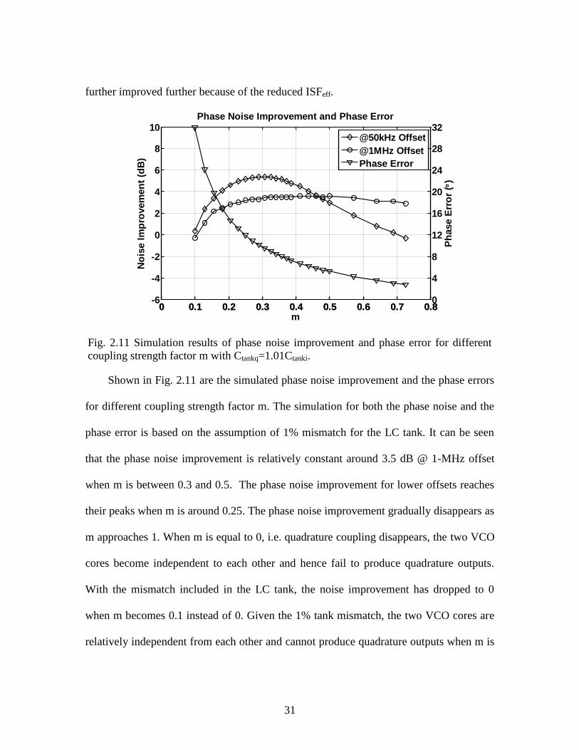
improvement beyond 3-dB theoretical prediction; especially the flicker noise can be
31
further improved further because of the reduced ISFeff.
Fig. 2.11 Simulation results of phase noise improvement and phase error for different
coupling strength factor m with Ctankq=1.01Ctanki.
Shown in Fig. 2.11 are the simulated phase noise improvement and the phase errors
for different coupling strength factor m. The simulation for both the phase noise and the
phase error is based on the assumption of 1% mismatch for the LC tank. It can be seen
that the phase noise improvement is relatively constant around 3.5 dB @ 1-MHz offset
when m is between 0.3 and 0.5. The phase noise improvement for lower offsets reaches
their peaks when m is around 0.25. The phase noise improvement gradually disappears as
m approaches 1. When m is equal to 0, i.e. quadrature coupling disappears, the two VCO
cores become independent to each other and hence fail to produce quadrature outputs.
With the mismatch included in the LC tank, the noise improvement has dropped to 0
when m becomes 0.1 instead of 0. Given the 1% tank mismatch, the two VCO cores are
relatively independent from each other and cannot produce quadrature outputs when m is
0 0.1 0.2 0.3 0.4 0.5 0.6 0.7 0.8-6
-4
-2
0
2
4
6
8
10
No
ise I
mp
rovem
en
t (d
B)
m
Phase Noise Improvement and Phase Error
0 0.1 0.2 0.3 0.4 0.5 0.6 0.7 0.80
4
8
12
16
20
24
28
32
Ph
ase E
rro
r (
)
@50kHz Offset
@1MHz Offset
Phase Error
32
smaller than 0.1. On the other hand, the phase error increase rapidly as m approaches 0.
Therefore, there is an optimum point of m to achieve the best phase noise improvement
with acceptable phase error. Furthermore, the VCO design cares more about the out-of-
band noise at large offset frequency since the close-in noise can be filtered by the phase-
locked-loop (PLL). Considering all the factors described above, the coupling strength
factor of 0.4 is chosen to implement the proposed CC-QVCO.
C
R
L
Gm(s)
Gc(s)
C
R
L
Gm(s)
-Gc(s)
A
B
I1
I2
C
R
L
-1/Gm(s)
± j/Gc(s)
(a) (b)
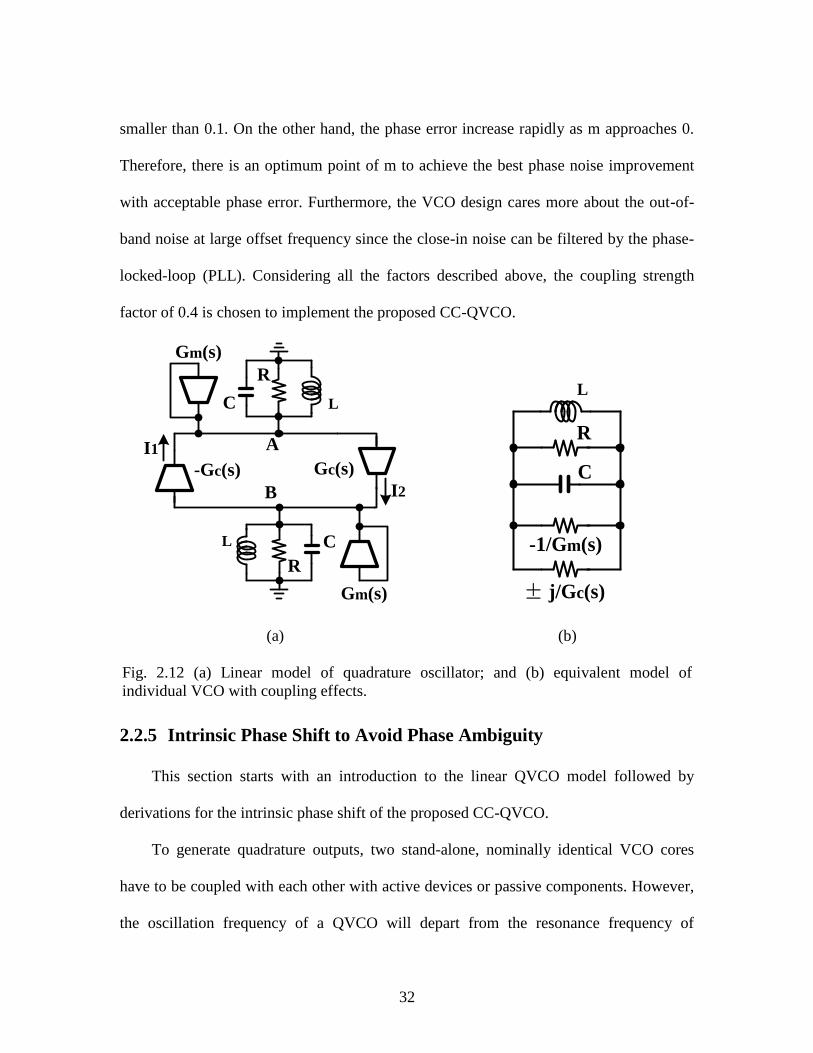
Fig. 2.12 (a) Linear model of quadrature oscillator; and (b) equivalent model of
individual VCO with coupling effects.
2.2.5 Intrinsic Phase Shift to Avoid Phase Ambiguity
This section starts with an introduction to the linear QVCO model followed by
derivations for the intrinsic phase shift of the proposed CC-QVCO.
To generate quadrature outputs, two stand-alone, nominally identical VCO cores
have to be coupled with each other with active devices or passive components. However,
the oscillation frequency of a QVCO will depart from the resonance frequency of
33
individual VCO cores because of the coupling mechanisms. The behavior of the two
VCO cores including coupling effects can be modeled by a simplified linear model [8]
[17] [19], as shown in Fig. 2.12 (a), where Gm(s) provides a negative resistance
compensating the energy loss due to the equivalent resistance R of a LC tank, and Gc(s)
represents the transconductance of the coupling mechanism between the two VCO cores.
Fig. 2.12 (b) presents the equivalent model for each VCO with quadrature-coupling
mechanism. Since one VCO core may lead or lag the other VCO core by 90º phase, ±j is
introduced to the coupling transconductance. For a conventional QVCO with parallel
coupling transistors [13], the frequency deviation can be found with steady state analysis
as
( )
(2.15)
where the positive or negative sign depends on whether the iVCO leads or lags the qVCO
by 90º; ω0 is the resonance frequency of individual LC tank; C is the capacitor of the LC
tank; and Gc is the equivalent transconductance of the quadrature-coupling mechanism
between the two VCO cores. From Equation (2.15), it is obvious that the larger the Gc is,
the larger the frequency deviation from ω0 becomes, which worsens the quality factor of
the LC tank. It is desirable to decrease the coupling strength to improve the phase noise
performance. The trade-off between the phase noise and phase error calls for a solution
that can maintain the phase noise performance without sacrificing the phase error.
Another commonly seen problem for a QVCO design is the phase ambiguity, i.e.,
the phase relations between the QVCO outputs could be either +90º or -90º. It is essential
to provide 90º-quadrature phase signals with deterministic phase relationship since a
34
receiver or transmitter which has been hard-wired to the QVCO outputs cannot
distinguish complex signals if the output phases are ambiguous, i.e. the wanted sideband
might be suppressed and instead the image signal might be detected after the image
rejection receiver. Although the asymmetry between two VCO cores can help the QVCO
to operate in one of the two stable modes, the bimodal oscillation can still exist due to
PVT variations. Usually, a phase shifter could be introduced in the quadrature-coupling
path to allow only one deterministic stable quadrature outputs, either +90º or -90º [16]-
[20]. To allow only one modal oscillation, the phase shift can be introduced by using
cascode transistor [16]. From theoretical point of view, 90º-phase shift in the coupling
path achieves not only the minimum phase noise performance, but also the best tolerance
to component mismatches between the two VCO cores [18], [19]. However, those
coupling mechanism with phase shifter still deteriorate the phase noise performance
because of the extra noise from the coupling transistors.
The noise degradation and phase ambiguity between the two VCO cores can be
solved simultaneously with the proposed Colpitts CC-QVCO. The CC-QVCO has an
intrinsic phase shift in the quadrature-coupling path and it can avoid the problem
associated with the bimodal oscillation. To illustrate this effect, a linear model similar to
the one shown in Fig. 2.12 (a) needs to be developed. Unlike a conventional QVCO with
parallel coupling, the proposed CC-QVCO is based on Colpitts VCO structure and the
quadrature-coupling transconductance Gc(s) is not intuitive.
According to the linear model of Fig. 2.12 (a), the Gc(s) can be found by grounding
node B and applying a voltage source ∆V at node A. The Gc(s) can be defined as the ratio
35
of the current I2 flowing into ground to the voltage source applied at node A. Similar
method can be used to find the quadrature- coupling transconductance for the CC-QVCO.
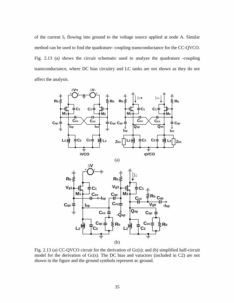
Fig. 2.13 (a) shows the circuit schematic used to analyze the quadrature -coupling
transconductance, where DC bias circuitry and LC tanks are not shown as they do not
affect the analysis.
C1
C2
C1
L2 L2
Isp Isn
Rb Rb
CqcCqcCcc Ccc
M1 M2
C1 C1
L2 L2
Qsp Qsn
Isp Isn
Rb Rb
CqcCqcCcc Ccc
M3 M4
C2 C2 C2
∆V-
Zb1 Zb1
∆V+
IC+ IC-
iVCO qVCO (a)
C1
C2L2
Isp
Rb
Cqc
Cqc
Ccc
Ccc
M1
C1
L2
Qsp
Rb
Cqc
Ccc
M3
C2
∆V
IC
-Isp
Rb
-Qsp
Ccc
Cqc
Rb
RbCcc Cqc
-Isp
Vg1 Vg3
Vg0
(b)
Fig. 2.13 (a) CC-QVCO circuit for the derivation of Gc(s); and (b) simplified half-circuit
model for the derivation of Gc(s). The DC bias and varactors (included in C2) are not
shown in the figure and the ground symbols represent ac ground.
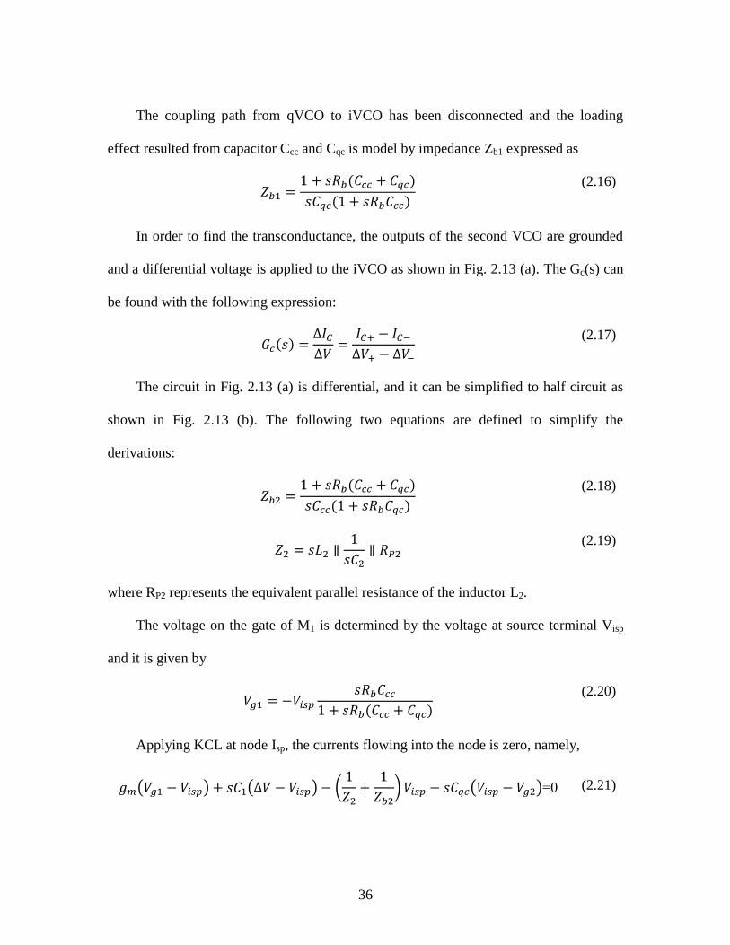
36
The coupling path from qVCO to iVCO has been disconnected and the loading
effect resulted from capacitor Ccc and Cqc is model by impedance Zb1 expressed as
( )
( )
(2.16)
In order to find the transconductance, the outputs of the second VCO are grounded
and a differential voltage is applied to the iVCO as shown in Fig. 2.13 (a). The Gc(s) can
be found with the following expression:
( )
(2.17)
The circuit in Fig. 2.13 (a) is differential, and it can be simplified to half circuit as
shown in Fig. 2.13 (b). The following two equations are defined to simplify the
derivations:
( )
( )
(2.18)
(2.19)
where RP2 represents the equivalent parallel resistance of the inductor L2.
The voltage on the gate of M1 is determined by the voltage at source terminal Visp
and it is given by
( )
(2.20)
Applying KCL at node Isp, the currents flowing into the node is zero, namely,
( ) ( ) (
* ( )=0 (2.21)
37
Similarly, the KCL equations for the node Vg2, Qsp, Vg0, and output can be written as
( )
( )
(2.22)
(
* ( )
(2.23)
( )
( )
(2.24)
( ) (2.25)
Replacing the Vg1 and Vg2 with the value obtained from (20) and (22), respectively,
Equation (2.21) can be rewritten as:
(2.26)
=
[ ( )]
(2.27)
[ ( )]
(2.28)
From Equation (2.22) and (2.24), it can be seen that Vg2 and Vg0 are of opposite
signs.
( )
( )
(2.29)
Combining Equation (2.23), (2.25), and (2.29), the solution for Visp and Vqsp can be
found as:
[
( )] (2.30)
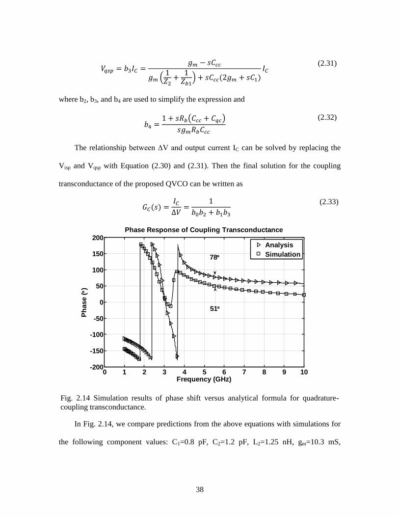
38
( ) ( )
(2.31)
where b2, b3, and b4 are used to simplify the expression and
( )
(2.32)
The relationship between ∆V and output current IC can be solved by replacing the
Visp and Vqsp with Equation (2.30) and (2.31). Then the final solution for the coupling
transconductance of the proposed QVCO can be written as
( )
(2.33)
Fig. 2.14 Simulation results of phase shift versus analytical formula for quadrature-
coupling transconductance.
In Fig. 2.14, we compare predictions from the above equations with simulations for
the following component values: C1=0.8 pF, C2=1.2 pF, L2=1.25 nH, gm=10.3 mS,
0 1 2 3 4 5 6 7 8 9 10-200
-150
-100
-50
0
50
100
150
200
Frequency (GHz)
Ph
ase ()
Phase Response of Coupling Transconductance
Analysis
Simulation78
51
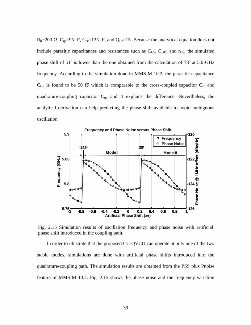
39
Rb=200 Ω, Cqc=95 fF, Ccc=135 fF, and QL2=15. Because the analytical equation does not
include parasitic capacitances and resistances such as CGS, CGD, and rDS, the simulated
phase shift of 51º is lower than the one obtained from the calculation of 78º at 5.6-GHz
frequency. According to the simulation done in MMSIM 10.2, the parasitic capacitance
CGS is found to be 50 fF which is comparable to the cross-coupled capacitor Ccc and
quadrature-coupling capacitor Cqc and it explains the difference. Nevertheless, the
analytical derivation can help predicting the phase shift available to avoid ambiguous
oscillation.
Fig. 2.15 Simulation results of oscillation frequency and phase noise with artificial
phase shift introduced in the coupling path.
In order to illustrate that the proposed CC-QVCO can operate at only one of the two
stable modes, simulations are done with artificial phase shifts introduced into the
quadrature-coupling path. The simulation results are obtained from the PSS plus Pnoise
feature of MMSIM 10.2. Fig. 2.15 shows the phase noise and the frequency variation
-1 -0.8 -0.6 -0.4 -0.2 0 0.2 0.4 0.6 0.8 15.75
5.8
5.85
5.9
Fre
qu
en
cy (
GH
z)
Artificial Phase Shift (x)
Frequency and Phase Noise versus Phase Shift
Mode I Mode II
-1 -0.8 -0.6 -0.4 -0.2 0 0.2 0.4 0.6 0.8 1-126
-124
-122
-120
Ph
ase N
ois
e @
1M
Hz o
ffset
(dB
c/H
z)Frequency
Phase Noise
-1 -0.8 -0.6 -0.4 -0.2 0 0.2 0.4 0.6 0.8 1-126
-124
-122
-120
Ph
ase N
ois
e @
1M
Hz o
ffset
(dB
c/H
z)
-142 38
40
with artificial phase shift, where the separation region of mode I and mode II is at 38º and
-142º. When the artificial phase shift is between -142º and 38º, the output phase of i-VCO
lags that of the qVCO by 90º, which is defined as mode I. For mode II, the output phase
of iVCO leads qVCO by 90º. Without the 38º-phase margin, the region separating mode I
and mode II would be around 0º. In other words, the intrinsic phase shift of the CC-
QVCO has already shifted the separating region from 0º to 38º. Since the result of 38º is
obtained from large signal simulation, the practical safety margin for phase shift has been
dropped down compared with the ac simulation result of 51º. Moreover, the phase noise
is optimum around 0º-artificial phase shift as shown in Fig. 2.15. Therefore, the proposed
CC-QVCO achieves good phase noise performance with the intrinsic phase shift of 38º
introduced by the coupling path. On the other hand, the variations of the simulated phase
noise is less than 2.5 dB, that is to say, the phase noise performance is not so sensitive to
the variation of phase shift and the phase shift can be increased to leave more margin for
stable oscillation.
2.2.6 Quadrature Inaccuracy
Mismatches between the two VCO cores for quadrature generation cause the outputs
to deviate from ±90º condition and the amplitudes to be unequal. Compared with unequal
amplitude, phase accuracy between the quadrature outputs is the primary concern for
QVCO circuits since the amplitude mismatch has less impact on receiving or transmitting
mixers if limiting buffers are used. Conventional QVCO with parallel coupling is less
sensitive to component mismatch when the introduced phase shift in the coupling path is
around 90º [18]-[20]. According to this theory, the proposed CC-QVCO would show
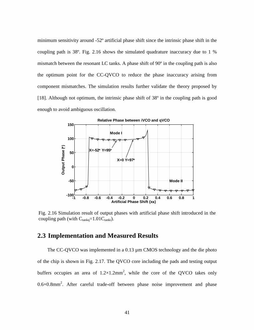
41
minimum sensitivity around -52º artificial phase shift since the intrinsic phase shift in the
coupling path is 38º. Fig. 2.16 shows the simulated quadrature inaccuracy due to 1 %
mismatch between the resonant LC tanks. A phase shift of 90º in the coupling path is also
the optimum point for the CC-QVCO to reduce the phase inaccuracy arising from
component mismatches. The simulation results further validate the theory proposed by
[18]. Although not optimum, the intrinsic phase shift of 38º in the coupling path is good
enough to avoid ambiguous oscillation.
Fig. 2.16 Simulation result of output phases with artificial phase shift introduced in the
coupling path (with Ctankq=1.01Ctanki).
2.3 Implementation and Measured Results
The CC-QVCO was implemented in a 0.13 µm CMOS technology and the die photo
of the chip is shown in Fig. 2.17. The QVCO core including the pads and testing output
buffers occupies an area of 1.2×1.2mm2, while the core of the QVCO takes only
0.6×0.8mm2. After careful trade-off between phase noise improvement and phase
-1 -0.8 -0.6 -0.4 -0.2 0 0.2 0.4 0.6 0.8 1-100
-50
0
50
100
150Relative Phase between iVCO and qVCO
Artificial Phase Shift (x)
Ou
tpu
t P
hase ()
Mode I
Mode II
X=-52 Y=95
X=0 Y=97
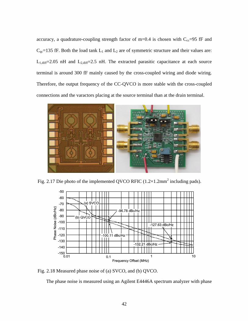
42
accuracy, a quadrature-coupling strength factor of m=0.4 is chosen with Ccc=95 fF and
Cqc=135 fF. Both the load tank L1 and L2 are of symmetric structure and their values are:
L1,diff=2.05 nH and L2,diff=2.5 nH. The extracted parasitic capacitance at each source
terminal is around 300 fF mainly caused by the cross-coupled wiring and diode wiring.
Therefore, the output frequency of the CC-QVCO is more stable with the cross-coupled
connections and the varactors placing at the source terminal than at the drain terminal.
Fig. 2.17 Die photo of the implemented QVCO RFIC (1.2×1.2mm2 including pads).
Fig. 2.18 Measured phase noise of (a) SVCO, and (b) QVCO.
The phase noise is measured using an Agilent E4446A spectrum analyzer with phase
-60
-50
-70
-80
-90
-110
-130
-100
-120
-140
-1500.01 0.1 1 10
Frequency Offset (MHz)
Ph
ase
No
ise
(d
Bc/H
z)
(a) SVCO
-96.78 dBc/Hz
-100.11 dBc/Hz
(b) QVCO
-127.63 dBc/Hz
-132.21 dBc/Hz
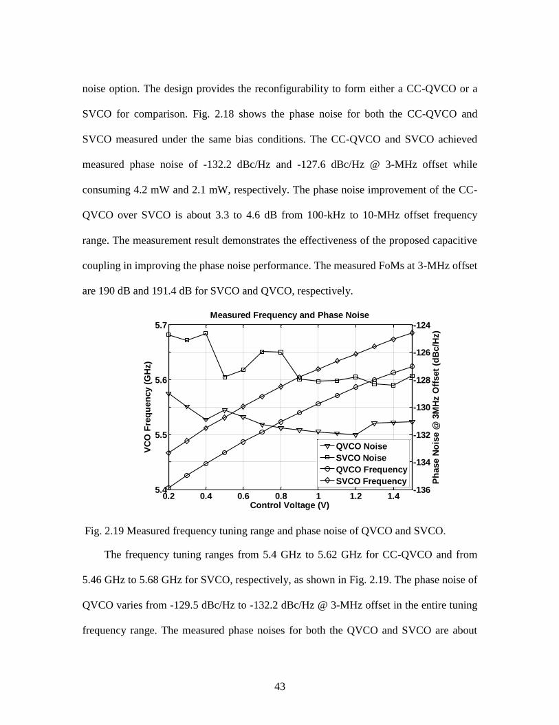
43
noise option. The design provides the reconfigurability to form either a CC-QVCO or a
SVCO for comparison. Fig. 2.18 shows the phase noise for both the CC-QVCO and
SVCO measured under the same bias conditions. The CC-QVCO and SVCO achieved
measured phase noise of -132.2 dBc/Hz and -127.6 dBc/Hz @ 3-MHz offset while
consuming 4.2 mW and 2.1 mW, respectively. The phase noise improvement of the CC-
QVCO over SVCO is about 3.3 to 4.6 dB from 100-kHz to 10-MHz offset frequency
range. The measurement result demonstrates the effectiveness of the proposed capacitive
coupling in improving the phase noise performance. The measured FoMs at 3-MHz offset
are 190 dB and 191.4 dB for SVCO and QVCO, respectively.
Fig. 2.19 Measured frequency tuning range and phase noise of QVCO and SVCO.
The frequency tuning ranges from 5.4 GHz to 5.62 GHz for CC-QVCO and from
5.46 GHz to 5.68 GHz for SVCO, respectively, as shown in Fig. 2.19. The phase noise of
QVCO varies from -129.5 dBc/Hz to -132.2 dBc/Hz @ 3-MHz offset in the entire tuning
frequency range. The measured phase noises for both the QVCO and SVCO are about
0.2 0.4 0.6 0.8 1 1.2 1.45.4
5.5
5.6
5.7
VC
O F
req
uen
cy (
GH
z)
0.2 0.4 0.6 0.8 1 1.2 1.4-136
-134
-132
-130
-128
-126
-124
Ph
ase N
ois
e @
3M
Hz O
ffset
(dB
c/H
z)
Control Voltage (V)
Measured Frequency and Phase Noise
QVCO Noise
SVCO Noise
QVCO Frequency
SVCO Frequency
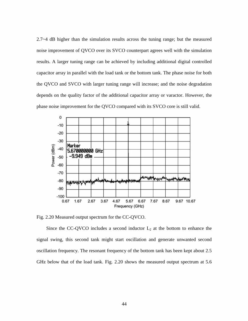
44
2.7~4 dB higher than the simulation results across the tuning range; but the measured
noise improvement of QVCO over its SVCO counterpart agrees well with the simulation
results. A larger tuning range can be achieved by including additional digital controlled
capacitor array in parallel with the load tank or the bottom tank. The phase noise for both
the QVCO and SVCO with larger tuning range will increase; and the noise degradation
depends on the quality factor of the additional capacitor array or varactor. However, the
phase noise improvement for the QVCO compared with its SVCO core is still valid.
Fig. 2.20 Measured output spectrum for the CC-QVCO.
Since the CC-QVCO includes a second inductor L2 at the bottom to enhance the
signal swing, this second tank might start oscillation and generate unwanted second
oscillation frequency. The resonant frequency of the bottom tank has been kept about 2.5
GHz below that of the load tank. Fig. 2.20 shows the measured output spectrum at 5.6
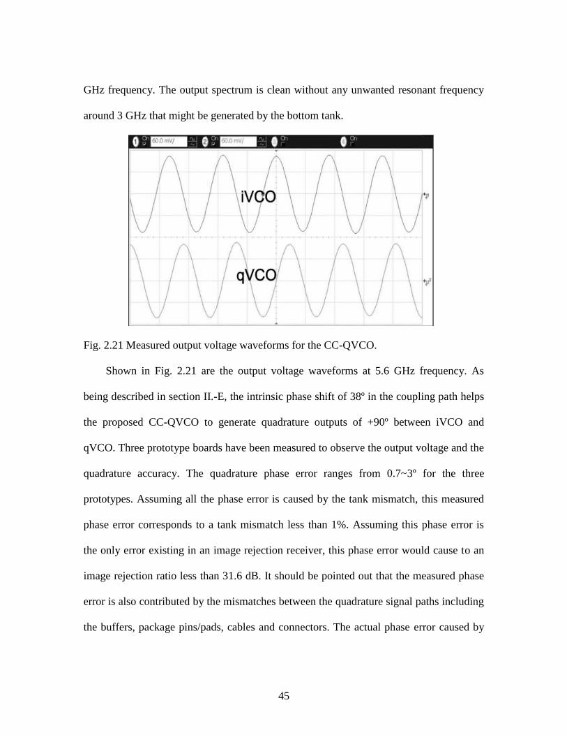
45
GHz frequency. The output spectrum is clean without any unwanted resonant frequency
around 3 GHz that might be generated by the bottom tank.
Fig. 2.21 Measured output voltage waveforms for the CC-QVCO.
Shown in Fig. 2.21 are the output voltage waveforms at 5.6 GHz frequency. As
being described in section II.-E, the intrinsic phase shift of 38º in the coupling path helps
the proposed CC-QVCO to generate quadrature outputs of +90º between iVCO and
qVCO. Three prototype boards have been measured to observe the output voltage and the
quadrature accuracy. The quadrature phase error ranges from 0.7~3º for the three
prototypes. Assuming all the phase error is caused by the tank mismatch, this measured
phase error corresponds to a tank mismatch less than 1%. Assuming this phase error is
the only error existing in an image rejection receiver, this phase error would cause to an
image rejection ratio less than 31.6 dB. It should be pointed out that the measured phase
error is also contributed by the mismatches between the quadrature signal paths including
the buffers, package pins/pads, cables and connectors. The actual phase error caused by
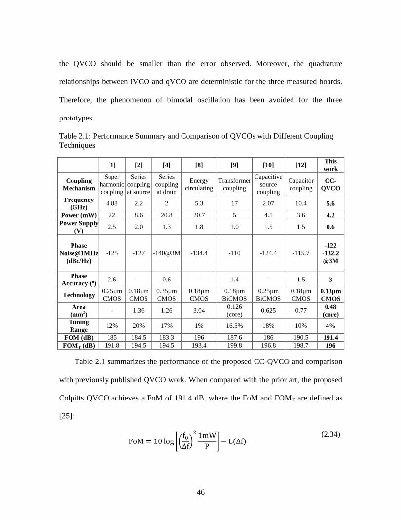
46
the QVCO should be smaller than the error observed. Moreover, the quadrature
relationships between iVCO and qVCO are deterministic for the three measured boards.
Therefore, the phenomenon of bimodal oscillation has been avoided for the three
prototypes.
Table 2.1: Performance Summary and Comparison of QVCOs with Different Coupling
Techniques
[1] [2] [4] [8] [9] [10] [12] This
work
Coupling
Mechanism
Super
harmonic
coupling
Series
coupling
at source
Series
coupling
at drain
Energy
circulating
Transformer
coupling
Capacitive
source
coupling
Capacitor
coupling CC-
QVCO
Frequency
(GHz) 4.88 2.2 2 5.3 17 2.07 10.4 5.6
Power (mW) 22 8.6 20.8 20.7 5 4.5 3.6 4.2
Power Supply
(V) 2.5 2.0 1.3 1.8 1.0 1.5 1.5 0.6
Phase
Noise@1MHz
(dBc/Hz)
-125 -127 -140@3M -134.4 -110 -124.4 -115.7 -122
-132.2
@3M
Phase
Accuracy (º) 2.6 - 0.6 - 1.4 - 1.5 3
Technology 0.25µm
CMOS
0.18µm
CMOS
0.35µm
CMOS
0.18µm
CMOS
0.18µm
BiCMOS
0.25µm
BiCMOS
0.18µm
CMOS 0.13µm
CMOS
Area
(mm2)
- 1.36 1.26 3.04 0.126
(core) 0.625 0.77
0.48
(core)
Tuning
Range 12% 20% 17% 1% 16.5% 18% 10% 4%
FOM (dB) 185 184.5 183.3 196 187.6 186 190.5 191.4
FOMT (dB) 191.8 194.5 194.5 193.4 199.8 196.8 198.7 196
Table 2.1 summarizes the performance of the proposed CC-QVCO and comparison
with previously published QVCO work. When compared with the prior art, the proposed
Colpitts QVCO achieves a FoM of 191.4 dB, where the FoM and FOMT are defined as
[25]:
[( *
] ( )
(2.34)
47
[ ( )
]
(2.35)
In the above equations, L(∆f) is the phase noise at the ∆f offset from the oscillator
frequency f0, P is the QVCO’s core power consumption in mW, TR is the relative tuning
range, and Vtune is the corresponding range of tuning voltage.
2.4 Conclusions
A CMOS enhance-swing Colpitts QVCO with capacitive coupling (CC-QVCO) for
noise reduction is proposed and analyzed in this chapter. The prototype CMOS CC-
QVCO was fabricated in 0.13 µm CMOS technology with measured frequency tuning
range about 4%. The CC-QVCO achieves a FoM of 191.4 dB while the FoM of a SVCO
of the same type is 190 dB. The phase noise improvement over SVCO is 3.3 dB and 4.6
dB at 100-kHz and 3-MHz offset, respectively. Moreover, the intrinsic phase shift in the
quadrature-coupling path has been analyzed, showing advantages of avoiding bimodal
oscillations for QVCO operations. The measurement results demonstrate not only the
effectiveness of the noise improvement using the proposed optimized capacitive-
coupling technique, but also the intrinsic phase shift that improves the stability of the CC-
QVCO. The CC-QVCO consumes only 4.2-mW power with a 0.6-V supply and occupies
a core area of 0.48 mm2.
48
3.1 Introduction
Quadrature signals are widely used in image-rejection transceivers [24] and half-rate
clock and data recovery (CDR) systems [38]. Among the many quadrature-signal
generation mechanisms [2]-[5], quadrature LC oscillator continues to be an attractive
research topic since the first publication of LC-QVCO on 1996 [6] [39] due to its low
phase noise performance. Several quadrature techniques have been developed in search
of improved phase noise performance, reduced phase accuracy, and elimination of bi-
modal oscillation, such as top/bottom series coupling, transformer-coupling, capacitive-
source coupling, and parallel coupling with phase shifters [6][8][9][18][37]. On the other
hand, coupling with active devices will either introduce extra noise source for parallel
coupling or lead to decreased voltage head room for top/bottom series coupling. However,
it is very challenging to design a QVCO that can completely remove the noise source in
the quadrature coupling device and avoid bi-modal oscillation simultaneously. A reliable
QVCO structure should have the following features:
A. The structure should be simple;
B. Introduces no extra noise in the quadrature coupling path;
Chapter 3 A 0.23-0.91° 4.3-5.27GHz NMOS LC CC-
QVCO without Bi-Modal Oscillation
49
C. Provides deterministic quadrature outputs;
D. Offers phase noise performance close or better than its single-phase counterpart,
E. Offers good phase accuracy over wide frequency tuning range .
In order to design a robust QVCO that can meet all those goals, it is desirable to
utilize innovative techniques. In this chapter, a quadrature LC VCO using capacitive-
coupling technique combined with source degeneration capacitor is proposed to offer low
phase noise performance, deterministic quadrature outputs, and excellent phase accuracy
over wide frequency range. Capacitive-coupling technique used for quadrature coupling
does not introduce extra noise from active devices. The utilization of source degeneration
capacitor introduces inherent leading phase delay in the quadrature-coupling path,
efficiently eliminating the phenomenon of the bi-modal oscillation.
This chapter is organized as follows. Section 3.2 analyzes important aspects for a
QVCO design. A capacitive-coupling QVCO with inherent leading phase shifter for the
elimination of bi-modal oscillation is proposed in Section 3.3. Linear model and mode
rejection ratio have been developed to evaluate the robustness of the proposed CC-QVCO
structure. Discussed in Section 3.4 are the design details of the proposed CC-QVCO and
corresponding simulation results to show its robustness. Besides, a SVCO counterpart
and a class-C mode TS-QVCO have been implemented for comparison. Experiment setup
and measurement results are given in Section 3.5. Finally, conclusion is drawn to
summarize this chapter.
3.2 Important Aspects of QVCO and Prior QVCO Structures
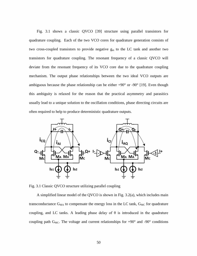
50
Fig. 3.1 shows a classic QVCO [39] structure using parallel transistors for
quadrature coupling. Each of the two VCO cores for quadrature generation consists of
two cross-coupled transistors to provide negative gm to the LC tank and another two
transistors for quadrature coupling. The resonant frequency of a classic QVCO will
deviate from the resonant frequency of its VCO core due to the quadrature coupling
mechanism. The output phase relationships between the two ideal VCO outputs are
ambiguous because the phase relationship can be either +90° or -90° [19]. Even though
this ambiguity is relaxed for the reason that the practical asymmetry and parasitics
usually lead to a unique solution to the oscillation conditions, phase directing circuits are
often required to help to produce deterministic quadrature outputs.
I+ I-
Q- Q+
Ib2Ib1
MC MCMA MA
Q+ Q-
I- I+
Ib2Ib1
MC MCMA MA
iAIiCQ iAQ
iCI
-1 -1
Fig. 3.1 Classic QVCO structure utilizing parallel coupling
A simplified linear model of the QVCO is shown in Fig. 3.2(a), which includes main
transconductance GMA to compensate the energy loss in the LC tank, GMC for quadrature
coupling, and LC tanks. A leading phase delay of θ is introduced in the quadrature
coupling path GMC. The voltage and current relationships for +90° and -90° conditions
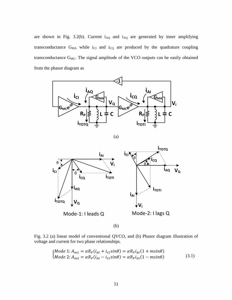
51
are shown in Fig. 3.2(b). Current iAQ and iAQ are generated by inner amplifying
transconductance GMA while iCI and iCQ are produced by the quadrature coupling
transconductance GMC. The signal amplitude of the VCO outputs can be easily obtained
from the phasor diagram as
-1
GMCejθ
GMA
RP CL
GMA
RP CL
iAQiCI
iAIiCQ
VIVQ
iTOTQ iTOTI
GMCejθ
(a)
iTOTQ
iAQ
iCI
VQ
VIθ
iTOTIiCQ
iAI
iTOTQ
iAI
iCQ
VI
VQ
iTOTI
iCI
iAQ
Mode-1: I leads Q
θ
θ
θ
Mode-2: I lags Q
(b)
Fig. 3.2 (a) linear model of conventional QVCO, and (b) Phasor diagram illustration of
voltage and current for two phase relationships.
( ) ( )
( ) ( ) (3.1)
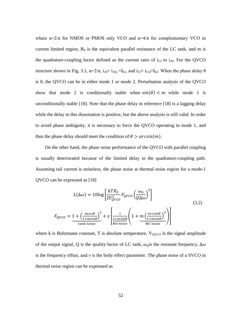
52
where α=2/π for NMOS or PMOS only VCO and α=4/π for complementary VCO in
current limited region, RP is the equivalent parallel resistance of the LC tank, and m is
the quadrature-coupling factor defined as the current ratio of iCI to iAI. For the QVCO
structure shown in Fig. 3.1, α=2/π, iAI= iAQ =Ib1, and iCI= iCQ=Ib2. When the phase delay θ
is 0, the QVCO can be in either mode 1 or mode 2. Perturbation analysis of the QVCO
show that mode 2 is conditionally stable when ( ) while mode 1 is
unconditionally stable [18]. Note that the phase delay in reference [18] is a lagging delay
while the delay in this dissertation is positive, but the above analysis is still valid. In order
to avoid phase ambiguity, it is necessary to force the QVCO operating in mode 1, and
thus the phase delay should meet the condition of ( ).
On the other hand, the phase noise performance of the QVCO with parallel coupling
is usually deteriorated because of the limited delay in the quadrature-coupling path.
Assuming tail current is noiseless, the phase noise at thermal noise region for a mode-1
QVCO can be expressed as [18]
( ) [
(
*
]
(
)
⏟
*
⏟
( (
)
⏟
)+
(3.2)
where k is Boltzmann constant, T is absolute temperature, VQVCO is the signal amplitude
of the output signal, Q is the quality factor of LC tank, is the resonant frequency,
is the frequency offset, and γ is the body effect parameter. The phase noise of a SVCO in
thermal noise region can be expressed as
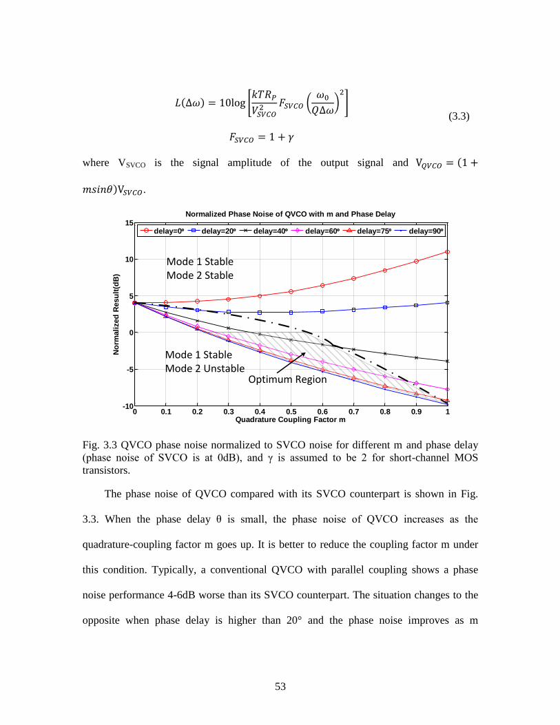
53
( ) [
(
*
]
(3.3)
where VSVCO is the signal amplitude of the output signal and (
) .
0 0.1 0.2 0.3 0.4 0.5 0.6 0.7 0.8 0.9 1-10
-5
0
5
10
15
Quadrature Coupling Factor m
No
rmali
zed
Resu
lt(d
B)
Normalized Phase Noise of QVCO with m and Phase Delay
delay=0 delay=20 delay=40 delay=60 delay=75 delay=90
Mode 1 StableMode 2 Unstable
Mode 1 StableMode 2 Stable
Optimum Region
Fig. 3.3 QVCO phase noise normalized to SVCO noise for different m and phase delay
(phase noise of SVCO is at 0dB), and γ is assumed to be 2 for short-channel MOS
transistors.
The phase noise of QVCO compared with its SVCO counterpart is shown in Fig.
3.3. When the phase delay θ is small, the phase noise of QVCO increases as the
quadrature-coupling factor m goes up. It is better to reduce the coupling factor m under
this condition. Typically, a conventional QVCO with parallel coupling shows a phase
noise performance 4-6dB worse than its SVCO counterpart. The situation changes to the
opposite when phase delay is higher than 20° and the phase noise improves as m
54
increases. The improvement becomes more obvious as phase delay is above 40°.
Therefore, stronger coupling factor is preferred for larger phase delay. However, there is
a boundary defined by ( ) which separates the stable region and ambiguous
region. In order to avoid phase ambiguity, it is desirable to choose m and phase delay
below the dashed boundary line shown in Fig. 3.3. The triangular gray box in Fig. 3.3
shows the optimum region which has better noise performance than its single-phase
counterpart and deterministic outputs.
Fig. 3.4 QVCO phase noise without MC devices normalized to QVCO noise with MC
devices for different m and phase delay, and γ is assumed to be 2 for short-channel MOS
transistors.
The phase noise performance of a conventional QVCO structure with θ=0 is worse
than its single-phase counterpart due to not only the quadrature coupling but also the
additional noise source in the quadrature-coupling path. Without the noise source in the
quadrature-coupling device, the phase noise in thermal noise region can be reduced to
0 0.1 0.2 0.3 0.4 0.5 0.6 0.7 0.8 0.9 1-4.5
-4
-3.5
-3
-2.5
-2
-1.5
-1
-0.5
0
Quadrature Coupling Factor m
No
rmali
zati
on
Resu
lts (
dB
)
Normalized Phase Noise of QVCO without MC Devices
delay=0
delay=20
delay=40
delay=60
delay=75
delay=90
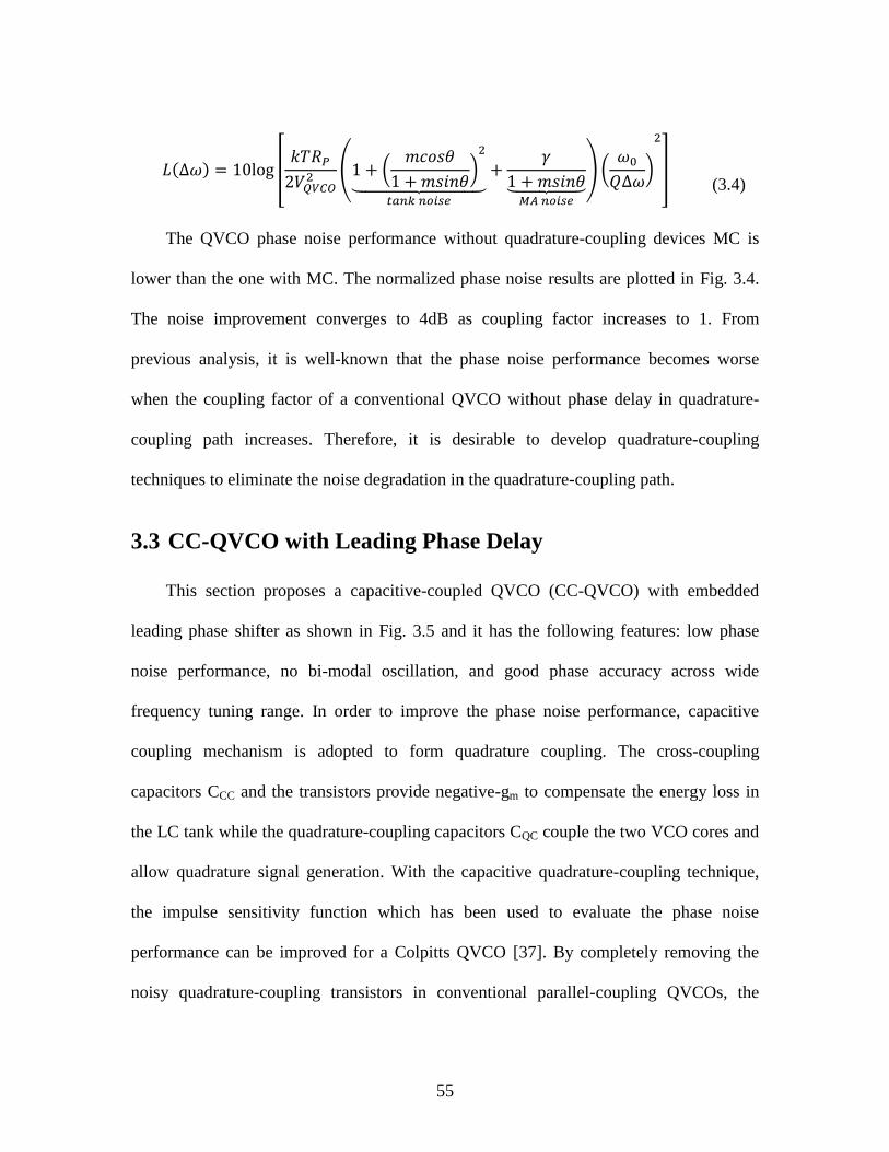
55
( ) [
( (
*
⏟
⏟
)(
*
] (3.4)
The QVCO phase noise performance without quadrature-coupling devices MC is
lower than the one with MC. The normalized phase noise results are plotted in Fig. 3.4.
The noise improvement converges to 4dB as coupling factor increases to 1. From
previous analysis, it is well-known that the phase noise performance becomes worse
when the coupling factor of a conventional QVCO without phase delay in quadrature-
coupling path increases. Therefore, it is desirable to develop quadrature-coupling
techniques to eliminate the noise degradation in the quadrature-coupling path.
3.3 CC-QVCO with Leading Phase Delay
This section proposes a capacitive-coupled QVCO (CC-QVCO) with embedded
leading phase shifter as shown in Fig. 3.5 and it has the following features: low phase
noise performance, no bi-modal oscillation, and good phase accuracy across wide
frequency tuning range. In order to improve the phase noise performance, capacitive
coupling mechanism is adopted to form quadrature coupling. The cross-coupling
capacitors CCC and the transistors provide negative-gm to compensate the energy loss in
the LC tank while the quadrature-coupling capacitors CQC couple the two VCO cores and
allow quadrature signal generation. With the capacitive quadrature-coupling technique,
the impulse sensitivity function which has been used to evaluate the phase noise
performance can be improved for a Colpitts QVCO [37]. By completely removing the
noisy quadrature-coupling transistors in conventional parallel-coupling QVCOs, the
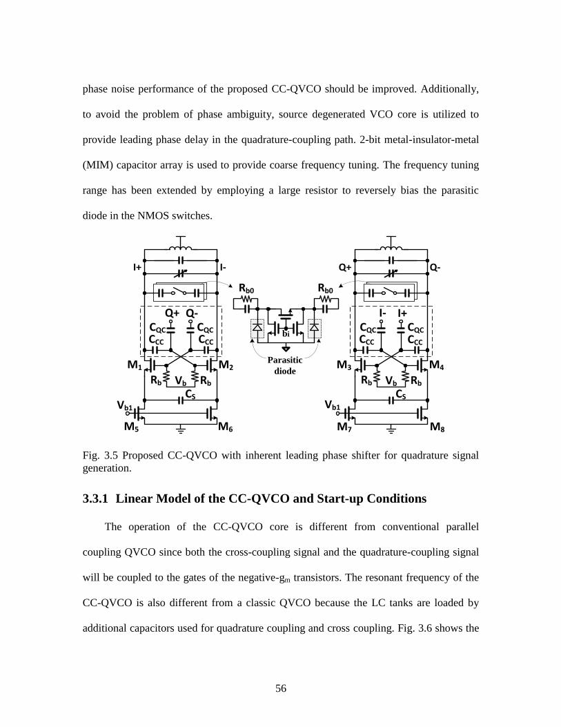
56
phase noise performance of the proposed CC-QVCO should be improved. Additionally,
to avoid the problem of phase ambiguity, source degenerated VCO core is utilized to
provide leading phase delay in the quadrature-coupling path. 2-bit metal-insulator-metal
(MIM) capacitor array is used to provide coarse frequency tuning. The frequency tuning
range has been extended by employing a large resistor to reversely bias the parasitic
diode in the NMOS switches.
I+ I-
Rb RbVb
CCC
CQC CQC
Vb1
CS
Q+ Q-
Q+ Q-
Rb RbVb
CCC
CQC CQC
CS
I- I+
M1 M2 M3 M4
CCC CCC
M5 M6 M7 M8
bi
Parasitic
diode
Rb0 Rb0
Vb1
Fig. 3.5 Proposed CC-QVCO with inherent leading phase shifter for quadrature signal
generation.
3.3.1 Linear Model of the CC-QVCO and Start-up Conditions
The operation of the CC-QVCO core is different from conventional parallel
coupling QVCO since both the cross-coupling signal and the quadrature-coupling signal
will be coupled to the gates of the negative-gm transistors. The resonant frequency of the
CC-QVCO is also different from a classic QVCO because the LC tanks are loaded by
additional capacitors used for quadrature coupling and cross coupling. Fig. 3.6 shows the
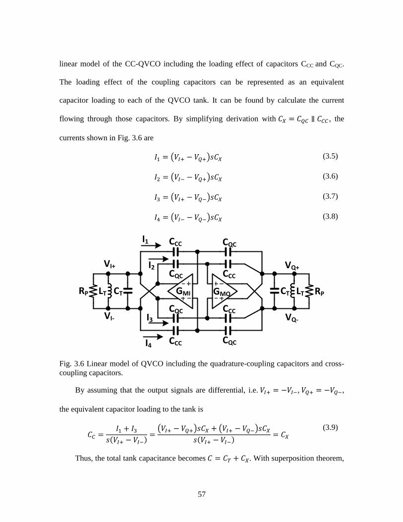
57
linear model of the CC-QVCO including the loading effect of capacitors CCC and CQC.
The loading effect of the coupling capacitors can be represented as an equivalent
capacitor loading to each of the QVCO tank. It can be found by calculate the current
flowing through those capacitors. By simplifying derivation with , the
currents shown in Fig. 3.6 are
( ) (3.5)
( ) (3.6)
( ) (3.7)
( ) (3.8)
CQC
CCC
CCC
CQC
CQC
CCC
CCC
CQC
GMI GMQ
VI+
RP RP
VI-
VQ+
VQ-
LT CT LTCT
I1
I2
I3
I4
Fig. 3.6 Linear model of QVCO including the quadrature-coupling capacitors and cross-
coupling capacitors.
By assuming that the output signals are differential, i.e. , ,
the equivalent capacitor loading to the tank is
( ) ( ) ( )
( )
(3.9)
Thus, the total tank capacitance becomes . With superposition theorem,
58
the current flowing out of the left transconductance GM can be expressed as
( )
( ) (3.10)
Therefore, the transconductance effect can be divided into two terms: the first term
on the right hand of the above equation represents the effect of negative gm used to start
the oscillator, and the second term represents the effect of quadrature coupling for
quadrature signal generation. Then an equivalent linear model for the proposed CC-
QVCO can be developed as shown in Fig. 3.7. The leading phase delay introduced by the
source degeneration capacitor is modeled as θ in the range of [0, 90°].
-1
GMCejθ
RP CL
iAI
iCQVI
iTOTI
GMAejθ
GMCejθ
RP CL
iAQ
iCIVQ
iTOTQ
GMAejθ
Fig. 3.7 Simplified linear model of the proposed QVCO with phase shifter.
By assuming the bias resistor Rb is large enough and its effect on the phase shifter
can be neglected, the effective cross-coupling transconductance and quadrature-coupling
transconductance are
(3.11)
(3.12)
where ( ) . Quadrature-coupling strength factor m is
59
redefined as
(3.13)
The loop gain based on the linear model is given by
( ) (
)
(3.14)
The real part and imaginary part of the term in the parentheses are
(
) (
)
( )
( )
(3.15)
(
) (
)
( )
( )
(3.16)
Barkhausen’s phase criteria should be met in order to sustain the oscillation
condition. Therefore, Equation (3.15) should equal to 0 and it leads to
(
*
(3.17)
The derivation of the above equation is based on the assumption that .
Inserting the above equation into Equation (3.16), the absolute value of the imaginary
part can be simplified as
| | |
|
(3.18)
Under oscillation condition, the absolute value of the imaginary part equals to 1 and
60
the condition for Barkhausen’s amplitude criteria is obtained as
( ) ( )
(3.19)
With Equation (3.17), the oscillation frequency of the CC-QVCO can be solved to
as
√(
*
(3.20)
where √ . Under the condition of , the first term of
right-hand side can be simplified with the approximation equation of .
(3.21)
Note that when the quality factor of the tank is much larger than 1, the first term of
the inner square root of Equation (3.20) is much smaller than the term and can be
neglected. Then the resonant frequency is approximated as
(3.22)
Similarly, the frequency deviation and oscillation frequency for the other condition
of can be solved as
(3.23)
(3.24)
Even though the special condition with θ≠0 assumed in the above derivation, the
analytical results also apply to the special condition of θ=0 and the resonant frequency
61
under such condition is ( ).
3.3.2 Mode Rejection for Stable Operation
The proposed CC-QVCO with inherent leading phase delay also has two stable
modes and each associates a different quadrature phase sequence. It is hazardous to use a
QVCO with ambiguous quadrature outputs to drive an image rejection receiver, because
it is unclear whether the upper or lower sideband will be selected. The voltage and
current relationship in the CC-QVCO is different from that of a conventional QVCO
because both the quadrature-coupling transconductance and the negative-gm stage have a
leading phase delay of θ. It is desirable to understand the effect of the phase delay on the
stability of the CC-QVCO.
Assuming the quadrature output voltages as ( ) ( ) and ( )
( ) with initial phase of 0, the voltage signals can be expressed in
exponential form as and
. Fig. 3.8 illustrates the voltages and
currents in the proposed QVCO. The signal amplitudes corresponding to the two stable
modes can be expressed as
( ) ( )
( ) ( ) (3.25)
where m is defined by Equation (3.13) and α is an coefficient including the effect of VCO
topology and source degeneration.
In practical applications, it is difficult to derive an accurate phase delay required to
completely eliminate the problem of bi-modal oscillation due to the asymmetry in the two
VCO cores since it is very challenging to develop an accurate QVCO model to include
62
the nonlinear effect resulted from large-signal operation. However, it is possible to find a
robust solution which shows high rejection to the unwanted mode. A mode rejection ratio
(MRR) representing a QVCO’s capability to reject the unwanted operation mode can be
simulated.
iTOTQ
iAQ
iCI
VQ
VI
θ
iTOTI
iCQ
iAI
iTOTQ
iAI
iCQ
VI
VQ
iTOTI
iCI iAQ
Mode-2: I lags Q
θ
θ
θ
Mode-1: I leads Q
θ
θ
Fig. 3.8 Phasor diagram of the voltage and current relationships in the proposed CC-
QVCO
First we can enhance the start-up gain for the unwanted mode by injecting energy
into the LC tank. The unwanted mode, assuming -90° mode, will start to oscillate with
the help of the artificially introduced energy. After the signal amplitude for -90° mode
reaches to some value AU, the energy injected can be removed immediately or damped
with high damping ratio. Then a robust QVCO should be able to attenuate the -90° mode
oscillation and gradually converges to +90° mode with signal amplitude of AW. It
requires that the QVCO to be able to provide higher loop gain for +90° mode than -90°
mode. The stronger the unwanted oscillation that an oscillator can reject, the more
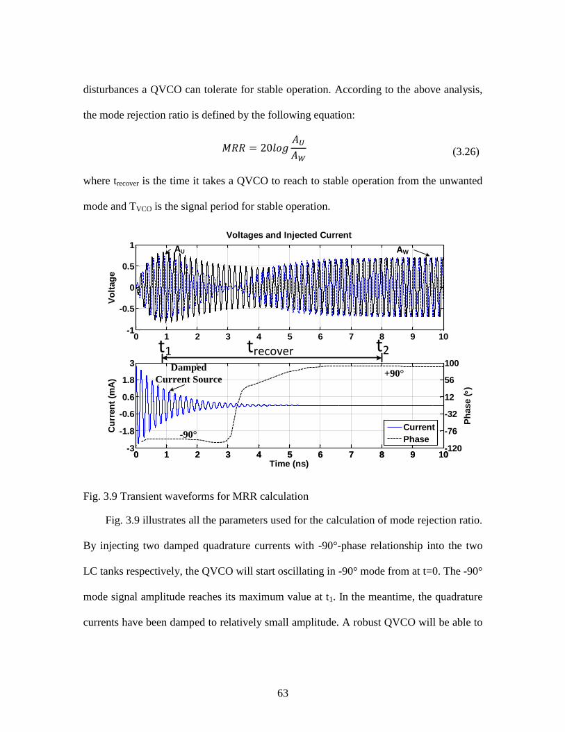
63
disturbances a QVCO can tolerate for stable operation. According to the above analysis,
the mode rejection ratio is defined by the following equation:
(3.26)
where trecover is the time it takes a QVCO to reach to stable operation from the unwanted
mode and TVCO is the signal period for stable operation.
0 1 2 3 4 5 6 7 8 9 10-1
-0.5
0
0.5
1
Vo
ltag
e
Voltages and Injected Current
0 1 2 3 4 5 6 7 8 9 10-3
-1.8
-0.6
0.6
1.8
3
Cu
rren
t (m
A)
Time (ns)
0 1 2 3 4 5 6 7 8 9 10-120
-76
-32
12
56
100
Ph
ase ()
Current
Phase
trecover
AWAU
-90°
+90° Damped
Current Source
t1 t2
Fig. 3.9 Transient waveforms for MRR calculation
Fig. 3.9 illustrates all the parameters used for the calculation of mode rejection ratio.
By injecting two damped quadrature currents with -90°-phase relationship into the two
LC tanks respectively, the QVCO will start oscillating in -90° mode from at t=0. The -90°
mode signal amplitude reaches its maximum value at t1. In the meantime, the quadrature
currents have been damped to relatively small amplitude. A robust QVCO will be able to
64
move away from -90° from t1 and then stabilize its +90° mode oscillation at t2. During the
time period t1~t2, the QVCO gradually converges to the wanted mode. The waveforms
shown in Fig. 3.9 have the following parameter: AU=0.73V, AW=0.7V, TVCO=182ps,
trecovery=7.2ns and
(3.27)
It means that the QVCO is able to tolerate an unwanted oscillation mode who is at
least 0.36dB higher than the wanted mode. The higher the MRR is, the better the
rejection to the unwanted disturbance. In order to find the maximum MRR for a specific
QVCO structure, the injecting energy needs to be gradually tuned to reach the boundary
condition.
3.4 Design and Simulation Results of a 5.6GHz CC-QVCO
3.4.1 Design Procedure of a CC-QVCO
The primary goal of a QVCO design is to provide deterministic quadrature outputs,
low phase noise performance, small phase accuracy, and tolerance to PVT variations. In
order to demonstrate the robustness of the capacitive-coupling technique, an example
CC-QVCO with leading phase shifter is implemented in a 130nm CMOS process.
Symmetrical spiral inductor with a size of 220×220µm2, realized on a 4-um-thick top
metal, is chosen for the resonant tank. The quality factor of the inductor plays key role in
achieving low phase noise performance and thus should be optimized by adjusting the
space, metal width, and outer dimension. The quality factor of the inductor has been
simulated for different size combinations at the target frequency. The differential quality
65
factor and inductance extraction used for inductor optimization is obtained from S-
parameters of two port simulation result defined by the following equations [40]:
(3.28)
(3.29)
( )
( )
( )
(3.30)
where R0 is the default single-ended port impedance. After optimization, the quality
factor of the 2-turn1.12nH inductor is 16 with metal space of 5µm and metal width of
15µm. Moreover, the quality factor of the LC tank including the varactor and capacitor
array is also optimized to achieve the best noise performance. Two-bit MIM capacitor
array is used to provide a coarse tuning range of 1GHz. In order to minimize the
degradation of quality factor, the switch with minimum length and width of 60µm is used
for coarse frequency tuning. According to reference [8], there exists a mutual inductance
M between the tanks of the two VCO cores. The strength of the coupling factor M is
dependent on the distance of the two inductors. In order to reduce the mutual inductance
which will deteriorate the phase error of the quadrature outputs, the distance between the
inductors is chosen to be 500µm. Other components such as transistors and capacitor
arrays are placed between the inductors.
The aspect ratio of the NMOS devices utilized to provide quadrature-coupling and
cross-coupling is chosen based on the matching properties and on the phase noise
performance. The length of the transistor is chosen to be twice the minimum length to
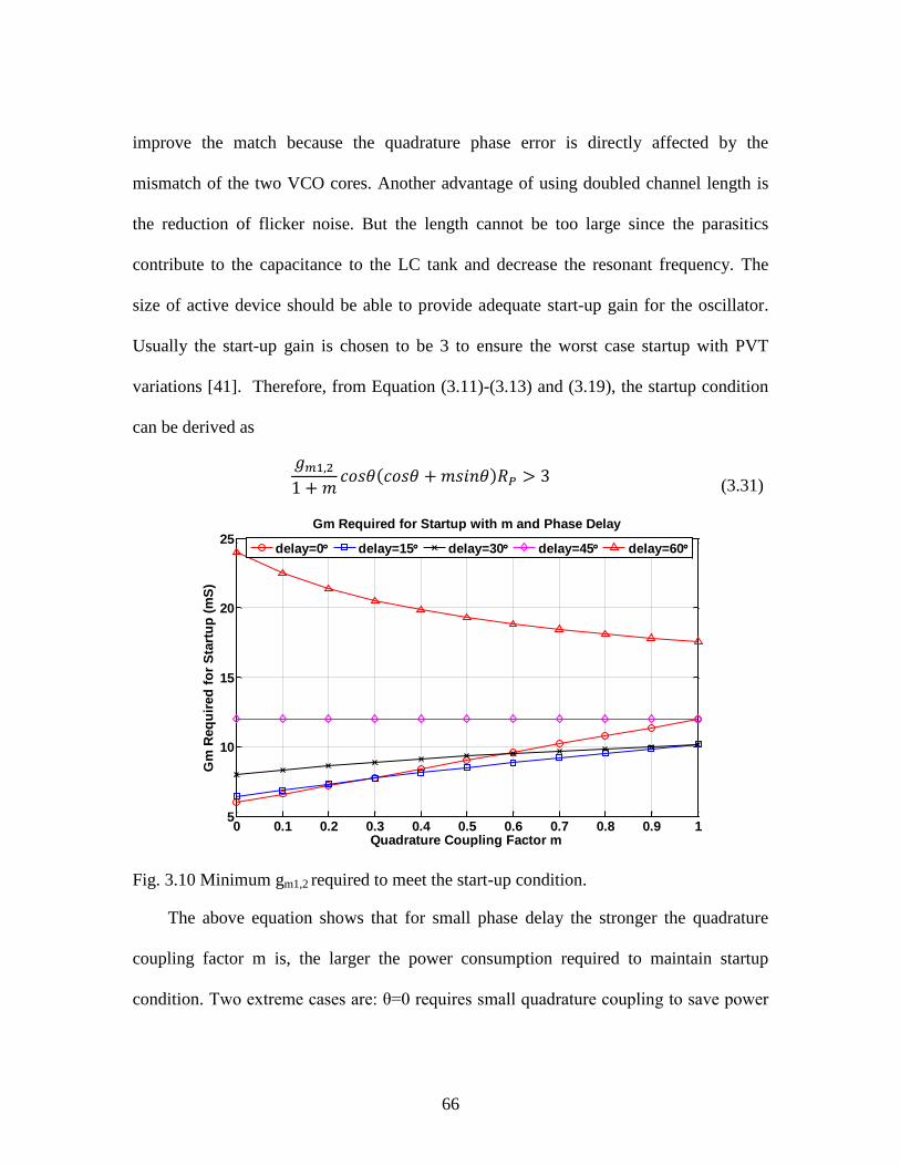
66
improve the match because the quadrature phase error is directly affected by the
mismatch of the two VCO cores. Another advantage of using doubled channel length is
the reduction of flicker noise. But the length cannot be too large since the parasitics
contribute to the capacitance to the LC tank and decrease the resonant frequency. The
size of active device should be able to provide adequate start-up gain for the oscillator.
Usually the start-up gain is chosen to be 3 to ensure the worst case startup with PVT
variations [41]. Therefore, from Equation (3.11)-(3.13) and (3.19), the startup condition
can be derived as
( ) (3.31)
Fig. 3.10 Minimum gm1,2 required to meet the start-up condition.
The above equation shows that for small phase delay the stronger the quadrature
coupling factor m is, the larger the power consumption required to maintain startup
condition. Two extreme cases are: θ=0 requires small quadrature coupling to save power
0 0.1 0.2 0.3 0.4 0.5 0.6 0.7 0.8 0.9 15
10
15
20
25
Quadrature Coupling Factor m
Gm
Req
uir
ed
fo
r S
tart
up
(m
S)
Gm Required for Startup with m and Phase Delay
delay=0 delay=15 delay=30 delay=45 delay=60
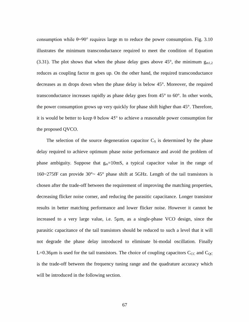
67
consumption while θ=90° requires large m to reduce the power consumption. Fig. 3.10
illustrates the minimum transconductance required to meet the condition of Equation
(3.31). The plot shows that when the phase delay goes above 45°, the minimum gm1,2
reduces as coupling factor m goes up. On the other hand, the required transconductance
decreases as m drops down when the phase delay is below 45°. Moreover, the required
transconductance increases rapidly as phase delay goes from 45° to 60°. In other words,
the power consumption grows up very quickly for phase shift higher than 45°. Therefore,
it is would be better to keep θ below 45° to achieve a reasonable power consumption for
the proposed QVCO.
The selection of the source degeneration capacitor CS is determined by the phase
delay required to achieve optimum phase noise performance and avoid the problem of
phase ambiguity. Suppose that gm=10mS, a typical capacitor value in the range of
160~275fF can provide 30°~ 45° phase shift at 5GHz. Length of the tail transistors is
chosen after the trade-off between the requirement of improving the matching properties,
decreasing flicker noise corner, and reducing the parasitic capacitance. Longer transistor
results in better matching performance and lower flicker noise. However it cannot be
increased to a very large value, i.e. 5µm, as a single-phase VCO design, since the
parasitic capacitance of the tail transistors should be reduced to such a level that it will
not degrade the phase delay introduced to eliminate bi-modal oscillation. Finally
L=0.36µm is used for the tail transistors. The choice of coupling capacitors CCC and CQC
is the trade-off between the frequency tuning range and the quadrature accuracy which
will be introduced in the following section.
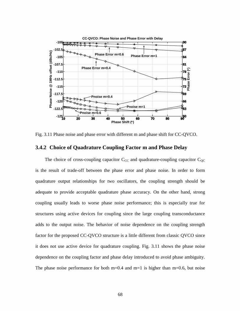
68
Fig. 3.11 Phase noise and phase error with different m and phase shift for CC-QVCO.
3.4.2 Choice of Quadrature Coupling Factor m and Phase Delay
The choice of cross-coupling capacitor CCC and quadrature-coupling capacitor CQC
is the result of trade-off between the phase error and phase noise. In order to form
quadrature output relationships for two oscillators, the coupling strength should be
adequate to provide acceptable quadrature phase accuracy. On the other hand, strong
coupling usually leads to worse phase noise performance; this is especially true for
structures using active devices for coupling since the large coupling transconductance
adds to the output noise. The behavior of noise dependence on the coupling strength
factor for the proposed CC-QVCO structure is a little different from classic QVCO since
it does not use active device for quadrature coupling. Fig. 3.11 shows the phase noise
dependence on the coupling factor and phase delay introduced to avoid phase ambiguity.
The phase noise performance for both m=0.4 and m=1 is higher than m=0.6, but noise
10 20 30 40 50 60 70 80 90-125
-122.5
-120
-117.5
-115
-112.5
-110
-107.5
-105
-102.5
-100
Ph
ase N
ois
e @
1M
Hz o
ffset
(dB
c/H
z)
Phase Shift ()
CC-QVCO: Phase Noise and Phase Error with Delay
10 20 30 40 50 60 70 80 9060
63
66
69
72
75
78
81
84
87
90
Ph
ase E
rro
r (
)
10 20 30 40 50 60 70 80 9060
63
66
69
72
75
78
81
84
87
90
10 20 30 40 50 60 70 80 9060
63
66
69
72
75
78
81
84
87
90
Pnoise m=0.6
Pnoise m=0.4
Pnoise m=1
Phase Error m=0.4
Phase Error m=0.6 Phase Error m=1
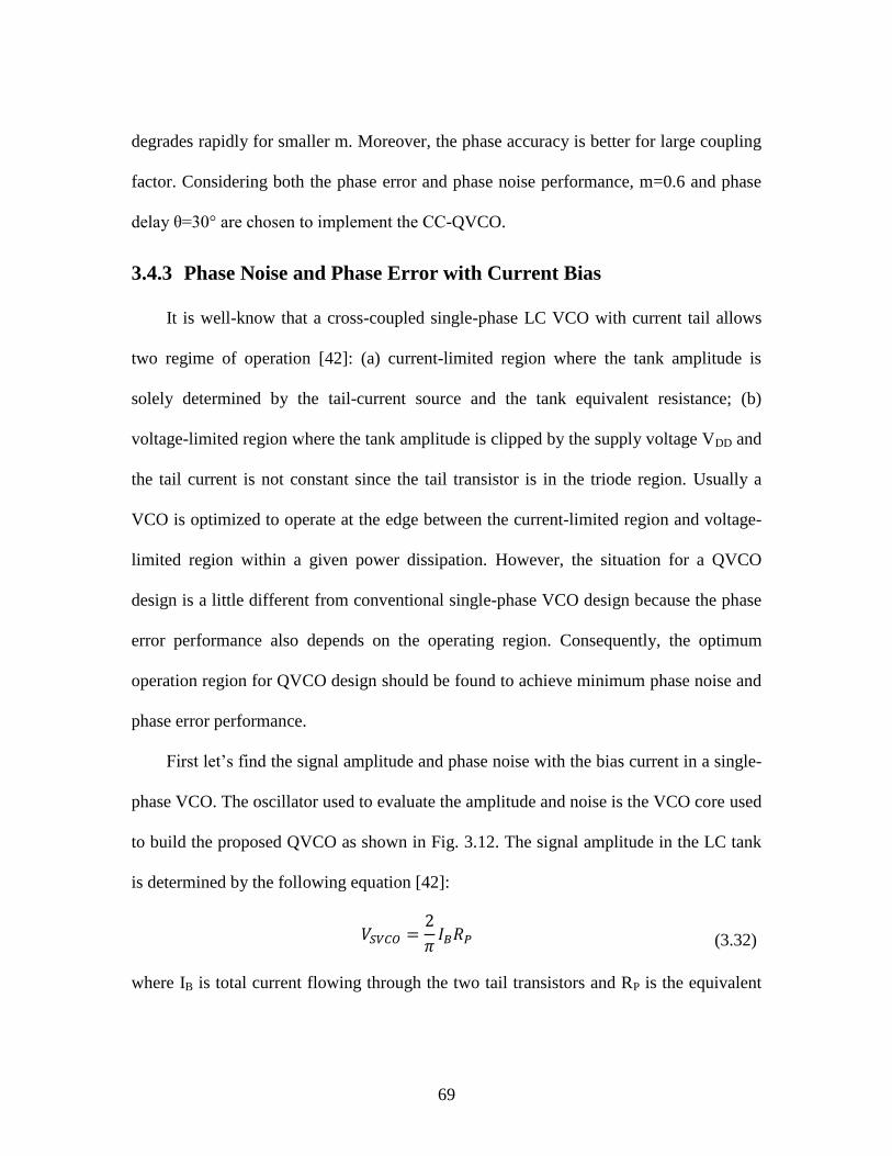
69
degrades rapidly for smaller m. Moreover, the phase accuracy is better for large coupling
factor. Considering both the phase error and phase noise performance, m=0.6 and phase
delay θ=30° are chosen to implement the CC-QVCO.
3.4.3 Phase Noise and Phase Error with Current Bias
It is well-know that a cross-coupled single-phase LC VCO with current tail allows
two regime of operation [42]: (a) current-limited region where the tank amplitude is
solely determined by the tail-current source and the tank equivalent resistance; (b)
voltage-limited region where the tank amplitude is clipped by the supply voltage VDD and
the tail current is not constant since the tail transistor is in the triode region. Usually a
VCO is optimized to operate at the edge between the current-limited region and voltage-
limited region within a given power dissipation. However, the situation for a QVCO
design is a little different from conventional single-phase VCO design because the phase
error performance also depends on the operating region. Consequently, the optimum
operation region for QVCO design should be found to achieve minimum phase noise and
phase error performance.
First let’s find the signal amplitude and phase noise with the bias current in a single-
phase VCO. The oscillator used to evaluate the amplitude and noise is the VCO core used
to build the proposed QVCO as shown in Fig. 3.12. The signal amplitude in the LC tank
is determined by the following equation [42]:
(3.32)
where IB is total current flowing through the two tail transistors and RP is the equivalent
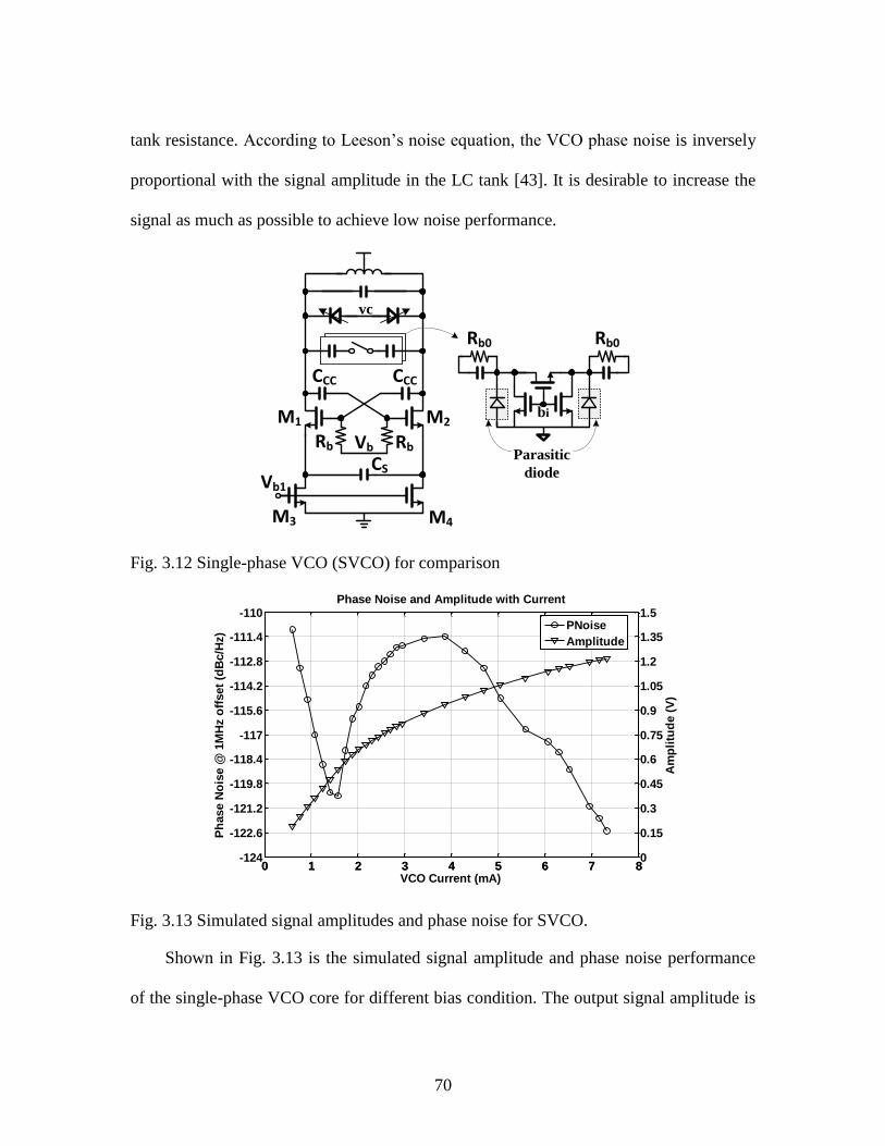
70
tank resistance. According to Leeson’s noise equation, the VCO phase noise is inversely
proportional with the signal amplitude in the LC tank [43]. It is desirable to increase the
signal as much as possible to achieve low noise performance.
Rb RbVb
CCC
Vb1
CS
M1
CCC
M3
M2bi
Parasitic
diode
vc
Rb0 Rb0
M4
Fig. 3.12 Single-phase VCO (SVCO) for comparison
Fig. 3.13 Simulated signal amplitudes and phase noise for SVCO.
Shown in Fig. 3.13 is the simulated signal amplitude and phase noise performance
of the single-phase VCO core for different bias condition. The output signal amplitude is
0 1 2 3 4 5 6 7 8-124
-122.6
-121.2
-119.8
-118.4
-117
-115.6
-114.2
-112.8
-111.4
-110
Ph
ase N
ois
e @
1M
Hz o
ffset
(dB
c/H
z)
VCO Current (mA)
Phase Noise and Amplitude with Current
0 1 2 3 4 5 6 7 80
0.15
0.3
0.45
0.6
0.75
0.9
1.05
1.2
1.35
1.5
Am
pli
tud
e (
V)
PNoise
Amplitude
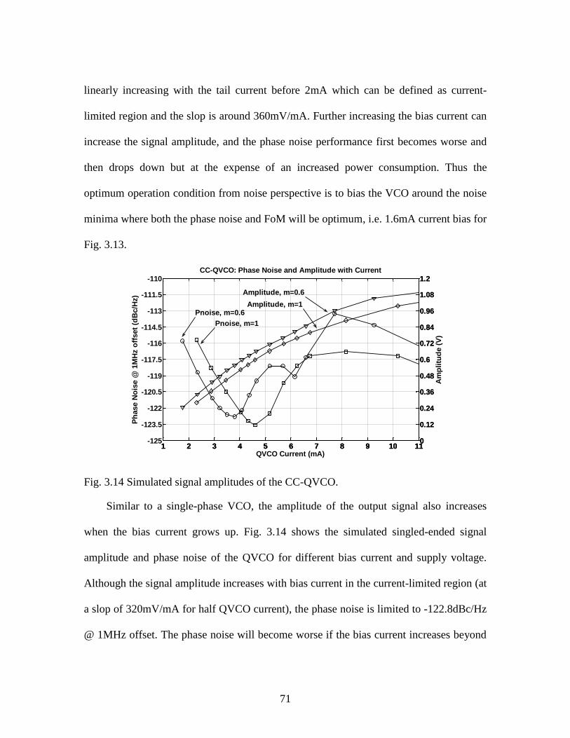
71
linearly increasing with the tail current before 2mA which can be defined as current-
limited region and the slop is around 360mV/mA. Further increasing the bias current can
increase the signal amplitude, and the phase noise performance first becomes worse and
then drops down but at the expense of an increased power consumption. Thus the
optimum operation condition from noise perspective is to bias the VCO around the noise
minima where both the phase noise and FoM will be optimum, i.e. 1.6mA current bias for
Fig. 3.13.
Fig. 3.14 Simulated signal amplitudes of the CC-QVCO.
Similar to a single-phase VCO, the amplitude of the output signal also increases
when the bias current grows up. Fig. 3.14 shows the simulated singled-ended signal
amplitude and phase noise of the QVCO for different bias current and supply voltage.
Although the signal amplitude increases with bias current in the current-limited region (at
a slop of 320mV/mA for half QVCO current), the phase noise is limited to -122.8dBc/Hz
@ 1MHz offset. The phase noise will become worse if the bias current increases beyond
1 2 3 4 5 6 7 8 9 10 11-125
-123.5
-122
-120.5
-119
-117.5
-116
-114.5
-113
-111.5
-110
Ph
ase N
ois
e @
1M
Hz o
ffset
(dB
c/H
z)
QVCO Current (mA)
CC-QVCO: Phase Noise and Amplitude with Current
1 2 3 4 5 6 7 8 9 10 110
0.12
0.24
0.36
0.48
0.6
0.72
0.84
0.96
1.08
1.2
Am
pli
tud
e (
V)
1 2 3 4 5 6 7 8 9 10 110
0.12
0.24
0.36
0.48
0.6
0.72
0.84
0.96
1.08
1.2
Pnoise, m=0.6
Amplitude, m=0.6
Amplitude, m=1
Pnoise, m=1
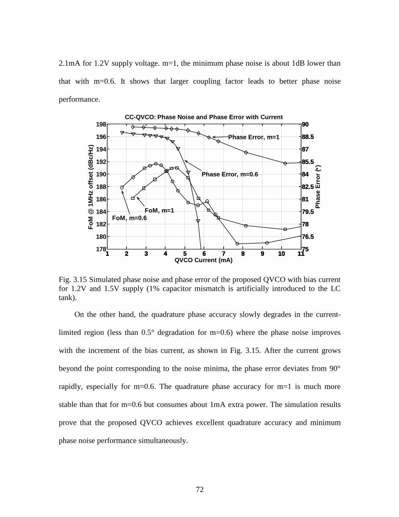
72
2.1mA for 1.2V supply voltage. m=1, the minimum phase noise is about 1dB lower than
that with m=0.6. It shows that larger coupling factor leads to better phase noise
performance.
Fig. 3.15 Simulated phase noise and phase error of the proposed QVCO with bias current
for 1.2V and 1.5V supply (1% capacitor mismatch is artificially introduced to the LC
tank).
On the other hand, the quadrature phase accuracy slowly degrades in the current-
limited region (less than 0.5° degradation for m=0.6) where the phase noise improves
with the increment of the bias current, as shown in Fig. 3.15. After the current grows
beyond the point corresponding to the noise minima, the phase error deviates from 90°
rapidly, especially for m=0.6. The quadrature phase accuracy for m=1 is much more
stable than that for m=0.6 but consumes about 1mA extra power. The simulation results
prove that the proposed QVCO achieves excellent quadrature accuracy and minimum
phase noise performance simultaneously.
1 2 3 4 5 6 7 8 9 10 11178
180
182
184
186
188
190
192
194
196
198
Fo
M @
1M
Hz o
ffset
(dB
c/H
z)
QVCO Current (mA)
CC-QVCO: Phase Noise and Phase Error with Current
1 2 3 4 5 6 7 8 9 10 1175
76.5
78
79.5
81
82.5
84
85.5
87
88.5
90
Ph
ase E
rro
r (
)
1 2 3 4 5 6 7 8 9 10 1175
76.5
78
79.5
81
82.5
84
85.5
87
88.5
90
FoM, m=1
FoM, m=0.6
Phase Error, m=0.6
Phase Error, m=1
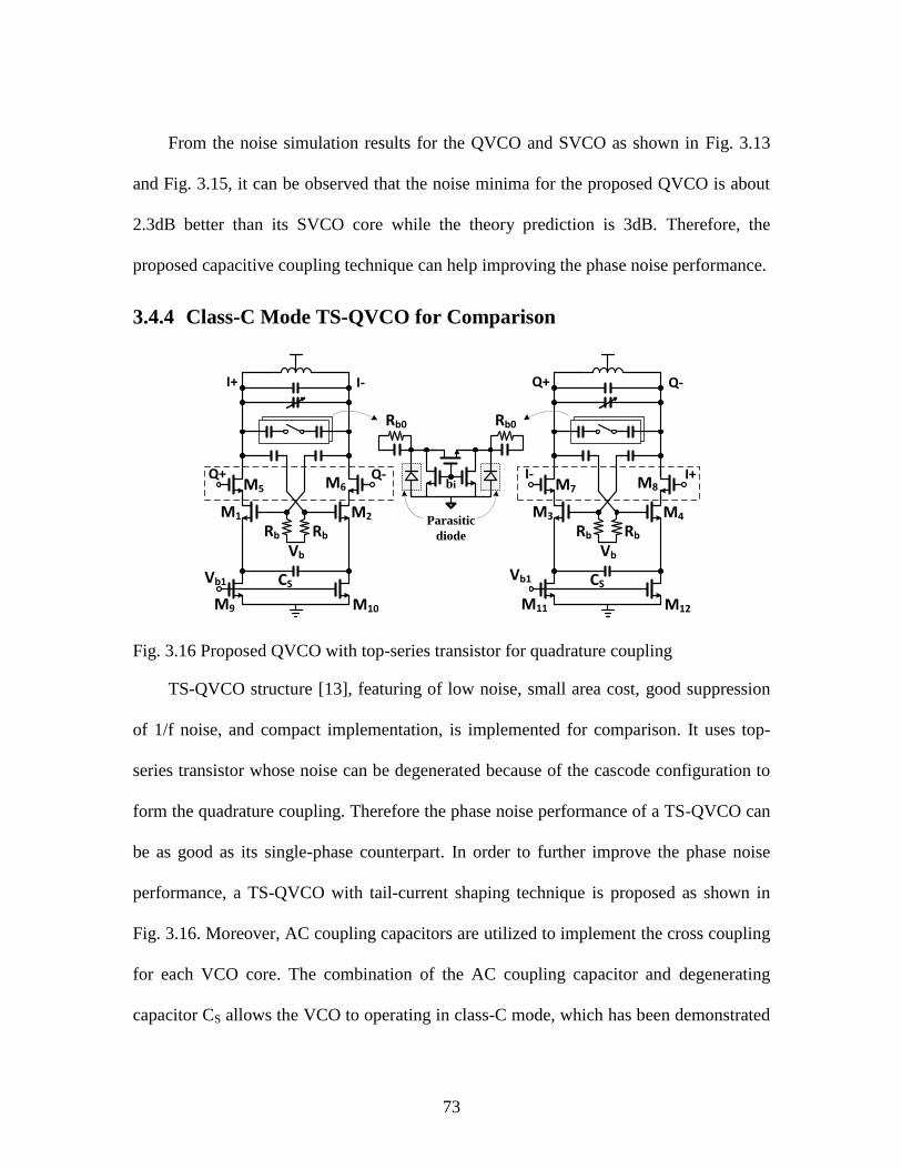
73
From the noise simulation results for the QVCO and SVCO as shown in Fig. 3.13
and Fig. 3.15, it can be observed that the noise minima for the proposed QVCO is about
2.3dB better than its SVCO core while the theory prediction is 3dB. Therefore, the
proposed capacitive coupling technique can help improving the phase noise performance.
3.4.4 Class-C Mode TS-QVCO for Comparison
I+ I-
Q+ Q-
Rb Rb
Vb
M1 M2
M5 M6
Vb1
M9 M10
CS
Q+ Q-
I- I+
Rb Rb
Vb
M3 M4
M7 M8
Vb1
M11 M12
CS
bi
Parasitic
diode
Rb0 Rb0
Fig. 3.16 Proposed QVCO with top-series transistor for quadrature coupling
TS-QVCO structure [13], featuring of low noise, small area cost, good suppression
of 1/f noise, and compact implementation, is implemented for comparison. It uses top-
series transistor whose noise can be degenerated because of the cascode configuration to
form the quadrature coupling. Therefore the phase noise performance of a TS-QVCO can
be as good as its single-phase counterpart. In order to further improve the phase noise
performance, a TS-QVCO with tail-current shaping technique is proposed as shown in
Fig. 3.16. Moreover, AC coupling capacitors are utilized to implement the cross coupling
for each VCO core. The combination of the AC coupling capacitor and degenerating
capacitor CS allows the VCO to operating in class-C mode, which has been demonstrated
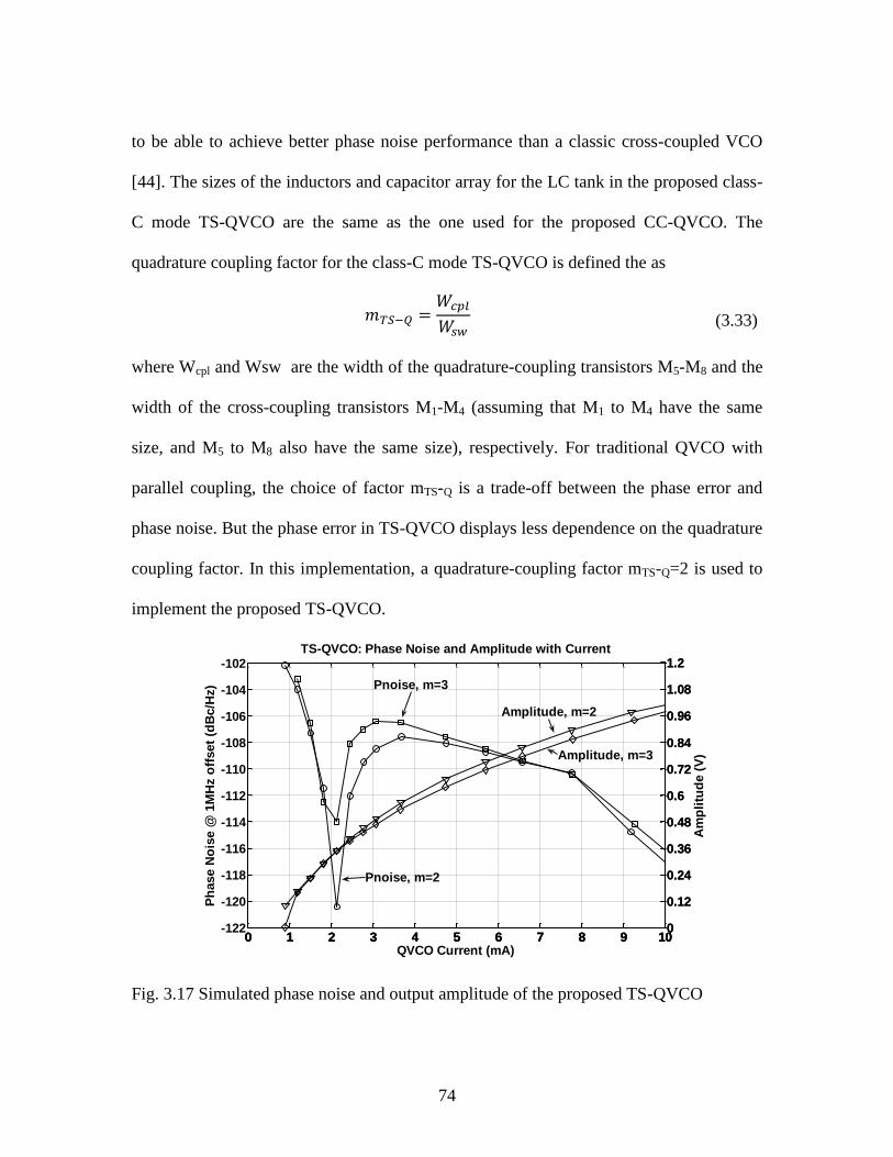
74
to be able to achieve better phase noise performance than a classic cross-coupled VCO
[44]. The sizes of the inductors and capacitor array for the LC tank in the proposed class-
C mode TS-QVCO are the same as the one used for the proposed CC-QVCO. The
quadrature coupling factor for the class-C mode TS-QVCO is defined the as
(3.33)
where Wcpl and Wsw are the width of the quadrature-coupling transistors M5-M8 and the
width of the cross-coupling transistors M1-M4 (assuming that M1 to M4 have the same
size, and M5 to M8 also have the same size), respectively. For traditional QVCO with
parallel coupling, the choice of factor mTS-Q is a trade-off between the phase error and
phase noise. But the phase error in TS-QVCO displays less dependence on the quadrature
coupling factor. In this implementation, a quadrature-coupling factor mTS-Q=2 is used to
implement the proposed TS-QVCO.
Fig. 3.17 Simulated phase noise and output amplitude of the proposed TS-QVCO
0 1 2 3 4 5 6 7 8 9 10-122
-120
-118
-116
-114
-112
-110
-108
-106
-104
-102
Ph
ase N
ois
e @
1M
Hz o
ffset
(dB
c/H
z)
QVCO Current (mA)
TS-QVCO: Phase Noise and Amplitude with Current
0 1 2 3 4 5 6 7 8 9 100
0.12
0.24
0.36
0.48
0.6
0.72
0.84
0.96
1.08
1.2
Am
pli
tud
e (
V)
0 1 2 3 4 5 6 7 8 9 100
0.12
0.24
0.36
0.48
0.6
0.72
0.84
0.96
1.08
1.2
Pnoise, m=3
Amplitude, m=2
Pnoise, m=2
Amplitude, m=3
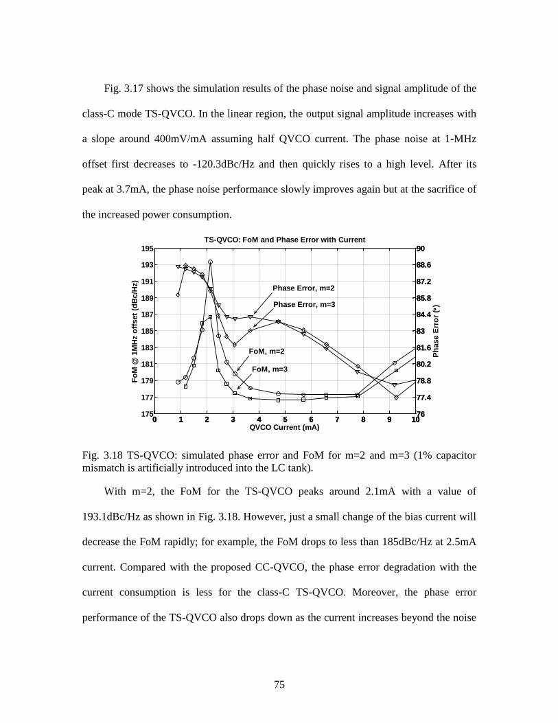
75
Fig. 3.17 shows the simulation results of the phase noise and signal amplitude of the
class-C mode TS-QVCO. In the linear region, the output signal amplitude increases with
a slope around 400mV/mA assuming half QVCO current. The phase noise at 1-MHz
offset first decreases to -120.3dBc/Hz and then quickly rises to a high level. After its
peak at 3.7mA, the phase noise performance slowly improves again but at the sacrifice of
the increased power consumption.
Fig. 3.18 TS-QVCO: simulated phase error and FoM for m=2 and m=3 (1% capacitor
mismatch is artificially introduced into the LC tank).
With m=2, the FoM for the TS-QVCO peaks around 2.1mA with a value of
193.1dBc/Hz as shown in Fig. 3.18. However, just a small change of the bias current will
decrease the FoM rapidly; for example, the FoM drops to less than 185dBc/Hz at 2.5mA
current. Compared with the proposed CC-QVCO, the phase error degradation with the
current consumption is less for the class-C TS-QVCO. Moreover, the phase error
performance of the TS-QVCO also drops down as the current increases beyond the noise
0 1 2 3 4 5 6 7 8 9 10175
177
179
181
183
185
187
189
191
193
195
Fo
M @
1M
Hz o
ffset
(dB
c/H
z)
QVCO Current (mA)
TS-QVCO: FoM and Phase Error with Current
0 1 2 3 4 5 6 7 8 9 1076
77.4
78.8
80.2
81.6
83
84.4
85.8
87.2
88.6
90
Ph
ase E
rro
r (
)
0 1 2 3 4 5 6 7 8 9 1076
77.4
78.8
80.2
81.6
83
84.4
85.8
87.2
88.6
90
Phase Error, m=2
FoM, m=3
FoM, m=2
Phase Error, m=3
76
minima point. Certainly the phase error performance should be improved by using larger
coupling factor m.
3.4.5 Performance Tolerance to Voltage and Temperature Variations
The practical environment for an integrated chip is usually complicated since the
ambient temperature and supply voltage may change for a portable device. The current
bias is also changing under different temperature or corner. Moreover, the performance of
a circuit is also affected by the fabrication process. Therefore, a robust QVCO should be
able to provide relatively constant performance over those variations. In order to prove
the robustness of the propose CC-QVCO, the variations of the phase noise and phase
error with voltage and temperature variations are discussed in this section. Several
simulations were run with spectreRF to compare the phase noise and phase error for the
proposed CC-QVCO and class-C mode TS-QVCO. The phase noise for the CC-QVCO
and its SVCO is also compared to show the robustness of the capacitive coupling
technique.
3.4.5.1 Impact of Bias Current and Supply
Typically the current bias of a QVCO is optimized for only a few target
applications; for example, minimum phase noise can be controlled by a few control bits
for different bands. However, the current changes with component accuracy, ambient
temperature, and fabrication process since and it requires complex automatic control
module to find the optimum setup for different frequency bands. Therefore, the
robustness of QVCO structure highly relies on its tolerance to the current and supply
change.
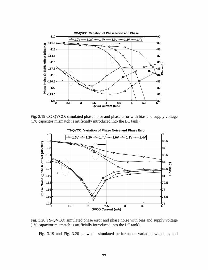
77
Fig. 3.19 CC-QVCO: simulated phase noise and phase error with bias and supply voltage
(1% capacitor mismatch is artificially introduced into the LC tank).
Fig. 3.20 TS-QVCO: simulated phase error and phase noise with bias and supply voltage
(1% capacitor mismatch is artificially introduced into the LC tank).
Fig. 3.19 and Fig. 3.20 show the simulated performance variation with bias and
2 2.5 3 3.5 4 4.5 5 5.5 6-125
-123.5
-122
-120.5
-119
-117.5
-116
-114.5
-113
-111.5
-110
Ph
ase N
ois
e @
1M
Hz o
ffset
(dB
c/H
z)
QVCO Current (mA)
CC-QVCO: Variation of Phase Noise and Phase
2 2.5 3 3.5 4 4.5 5 5.5 680
81
82
83
84
85
86
87
88
89
90
Ph
ase ()
1.0V 1.2V 1.4V 1.0V 1.2V 1.4V
1 1.5 2 2.5 3 3.5 4-122
-119
-116
-113
-110
-107
-104
-101
-98
-95
-92
Ph
ase N
ois
e @
1M
Hz o
ffset
(dB
c/H
z)
QVCO Current (mA)
TS-QVCO: Variation of Phase Noise and Phase Error
1 1.5 2 2.5 3 3.5 475
76.5
78
79.5
81
82.5
84
85.5
87
88.5
90
Ph
ase ()
1.0V 1.2V 1.4V 1.0V 1.2V 1.4V
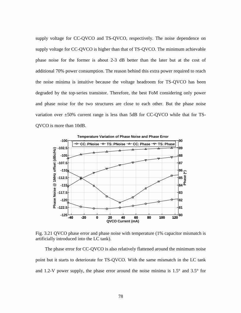
78
supply voltage for CC-QVCO and TS-QVCO, respectively. The noise dependence on
supply voltage for CC-QVCO is higher than that of TS-QVCO. The minimum achievable
phase noise for the former is about 2-3 dB better than the later but at the cost of
additional 70% power consumption. The reason behind this extra power required to reach
the noise minima is intuitive because the voltage headroom for TS-QVCO has been
degraded by the top-series transistor. Therefore, the best FoM considering only power
and phase noise for the two structures are close to each other. But the phase noise
variation over ±50% current range is less than 5dB for CC-QVCO while that for TS-
QVCO is more than 10dB.
Fig. 3.21 QVCO phase error and phase noise with temperature (1% capacitor mismatch is
artificially introduced into the LC tank).
The phase error for CC-QVCO is also relatively flattened around the minimum noise
point but it starts to deteriorate for TS-QVCO. With the same mismatch in the LC tank
and 1.2-V power supply, the phase error around the noise minima is 1.5° and 3.5° for
-40 -20 0 20 40 60 80 100 120-125
-122.5
-120
-117.5
-115
-112.5
-110
-107.5
-105
-102.5
-100
Ph
ase N
ois
e @
1M
Hz o
ffset
(dB
c/H
z)
QVCO Current (mA)
Temperature Variation of Phase Noise and Phase Error
-40 -20 0 20 40 60 80 100 12080
81
82
83
84
85
86
87
88
89
90
Ph
ase ()
CC: PNoise TS: PNoise CC: Phase TS: Phase
79
CC-QVCO and TS-QVCO, respectively. The proposed CC-QVCO demonstrates more
robust current tolerance than TS-QVCO according to the simulation results.
3.4.5.2 Tolerance to Temperature
Other parameters such as chip temperature, ambient environment, and fabrication
process also play important role on a QVCO performance. Most commercial applications
usually require a temperature range of 0~85. Simulation results of phase noise and
phase error with temperature range of -45~125 is shown in Fig. 3.21. Yet again the CC-
QVCO demonstrates better performance tolerance to temperature than the TS-QVCO
structure.
3.5 Implementation and Measurement Results
The proposed CC-QVCO, class-C mode TS-QVCO, and SVCO have been
fabricated in a 0.13-µm CMOS technology. The core areas for the three circuits are as
follows: ACC-QVCO=A TS-QVCO =1.0×0.35mm2 and 0.35×0.5mm
2 for SVCO. The inductors
for all the implemented oscillators are of the same size with a value of 1.12nH. Die
photos for the three oscillators are shown in Fig. 3.22. Diode varactors have been used to
achieve fine frequency tuning while the 2-bit MIM capacitor array are utilized for coarse
tuning. The layout of the quadrature-coupling path for the proposed QVCO has been
optimized to improve the matching since the mismatch in the coupling interconnections
directly affects the quadrature phase error. All measurements results have been performed
with a 1.2-V power supply if not specified. The phase noise and the output spectrum are
measured with spectrum analyzer E4446A.
80
CC-QVCO
TS-QVCO
SVCO
Fig. 3.22 Die photos of the implemented CC-QVCO, class-C mode TS-QVCO, and
SVCO.
Vin+
Vin-
Vb
Vb
BI+
BQ+BI-
BQ-
BI+
BI-
LOI+ LOI-
LOI- LOI+
BQ+
BQ-
LOQ+ LOQ-
LOQ- LOQ+
RF+ RF-
(a) (b)
Fig. 3.23 Auxiliary circuits for phase error measurement: (a) 4 stages of RC poly-phase
filter for IQ baseband signal generation, (b) upconversion mixer.
3.5.1 Upconversion Mixer and IF Baseband Signal Generation
Usually the sampling rate of an oscilloscope cannot provide adequate time
81
resolution to measure the quadrature accuracy at 5GHz, especially when the parasitics on
the board and losses in cable will add to the measurement error. As a result, the measured
phase accuracy using oscilloscope can be easily affected by the testing environment. One
of the most popular ways for measuring the quadrature phase error is to observe the
sideband rejection ratio after single-sideband upconversion mixer [6] [13]. This technique
requires a quadrature IF baseband signal, which can be generated from a RC poly-phase
filter. Fig. 3.23 (a) shows a four-stage off-chip RC poly-phase filter with same resistors
and capacitors utilized to generate IF quadrature signals. The resistors and capacitors are
configured in such a way that the wire mismatches between the IQ signal paths are small
since the error in the IQ paths directly influences the measurement accuracy. An on-chip
passive mixer as shown in Fig. 3.23 (b) is employed to upconvert the IF baseband signal
to VCO frequency. Then the phase error can be measured from the sideband rejection
ratio at the RF spectrum.
Fig. 3.24 Measured phase noise performance of the proposed CC-QVCO at 4.7GHz with
a 1.2V power supply and 8.5mA total current.
82
3.5.2 Phase Noise and Frequency Range
The measured phase noise performance for the proposed CC-QVCO is shown in Fig.
3.24. Under 1.2V supply voltage and 8.5mA, the CC-QVCO achieves a measured phase
noise of -124.04dBc/Hz @ 1-MHz offset with center frequency of 4.7GHz. The
corresponding FoM for this phase noise performance is 187.4dBc/Hz. Shown in Fig. 3.25
is the measured phase noise performance of the class-C mode TS-QVCO. It achieves a
measured phase noise performance of -121.05dBc/Hz @ 1-MHz offset with a center
frequency of 4.9GHz and the corresponding FoM is 184.52dBc/Hz. The measured phase
noise performance at 1-MHz offset for CC-QVCO is 3dB better than the TS-QVCO.
Fig. 3.25 Measured phase noise performance of the proposed TS-QVCO at 4.9GHz with
a 1.2V power supply and 9mA total current.
The phase noise of the implemented SVCO prototype is shown in Fig. 3.26. It
achieves a measured phase noise of -120.09dBc/Hz @ 1-MHz offset, consuming 4.6mA
from a 1.2V supply voltage. As a result, the phase noise performance of the proposed
CC-QVCO is 4dB better than that of the implemented SVCO.
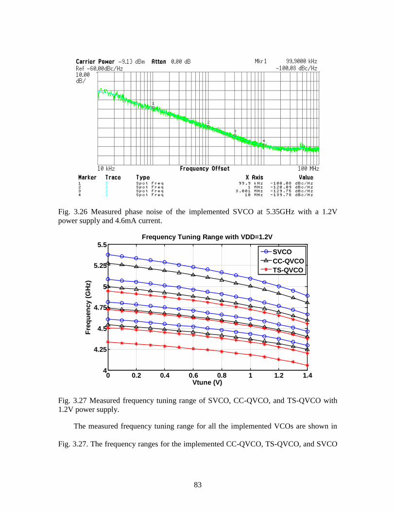
83
Fig. 3.26 Measured phase noise of the implemented SVCO at 5.35GHz with a 1.2V
power supply and 4.6mA current.
Fig. 3.27 Measured frequency tuning range of SVCO, CC-QVCO, and TS-QVCO with
1.2V power supply.
The measured frequency tuning range for all the implemented VCOs are shown in
Fig. 3.27. The frequency ranges for the implemented CC-QVCO, TS-QVCO, and SVCO
0 0.2 0.4 0.6 0.8 1 1.2 1.44
4.25
4.5
4.75
5
5.25
5.5
Vtune (V)
Fre
qu
en
cy (
GH
z)
Frequency Tuning Range with VDD=1.2V
SVCO
CC-QVCO
TS-QVCO
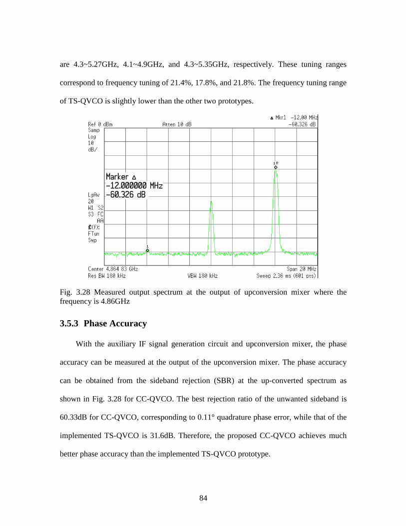
84
are 4.3~5.27GHz, 4.1~4.9GHz, and 4.3~5.35GHz, respectively. These tuning ranges
correspond to frequency tuning of 21.4%, 17.8%, and 21.8%. The frequency tuning range
of TS-QVCO is slightly lower than the other two prototypes.
Fig. 3.28 Measured output spectrum at the output of upconversion mixer where the
frequency is 4.86GHz
3.5.3 Phase Accuracy
With the auxiliary IF signal generation circuit and upconversion mixer, the phase
accuracy can be measured at the output of the upconversion mixer. The phase accuracy
can be obtained from the sideband rejection (SBR) at the up-converted spectrum as
shown in Fig. 3.28 for CC-QVCO. The best rejection ratio of the unwanted sideband is
60.33dB for CC-QVCO, corresponding to 0.11° quadrature phase error, while that of the
implemented TS-QVCO is 31.6dB. Therefore, the proposed CC-QVCO achieves much
better phase accuracy than the implemented TS-QVCO prototype.
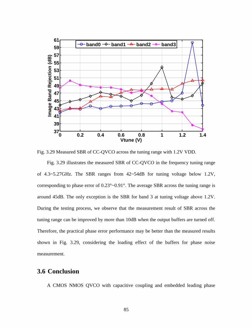
85
Fig. 3.29 Measured SBR of CC-QVCO across the tuning range with 1.2V VDD.
Fig. 3.29 illustrates the measured SBR of CC-QVCO in the frequency tuning range
of 4.3~5.27GHz. The SBR ranges from 42~54dB for tuning voltage below 1.2V,
corresponding to phase error of 0.23°~0.91°. The average SBR across the tuning range is
around 45dB. The only exception is the SBR for band 3 at tuning voltage above 1.2V.
During the testing process, we observe that the measurement result of SBR across the
tuning range can be improved by more than 10dB when the output buffers are turned off.
Therefore, the practical phase error performance may be better than the measured results
shown in Fig. 3.29, considering the loading effect of the buffers for phase noise
measurement.
3.6 Conclusion
A CMOS NMOS QVCO with capacitive coupling and embedded leading phase
0 0.2 0.4 0.6 0.8 1 1.2 1.437
39
41
43
45
47
49
51
53
55
57
59
61
Vtune (V)
Imag
e B
an
d R
eje
cti
on
(d
B)
band0 band1 band2 band3
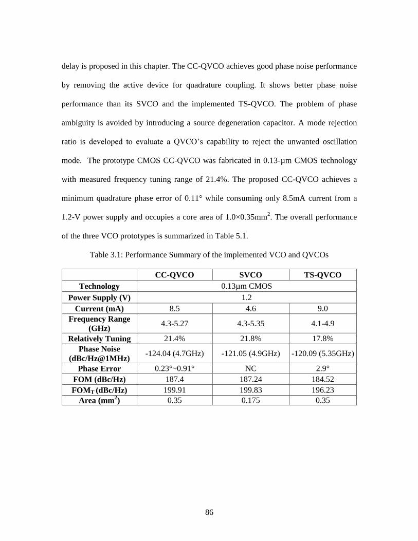
86
delay is proposed in this chapter. The CC-QVCO achieves good phase noise performance
by removing the active device for quadrature coupling. It shows better phase noise
performance than its SVCO and the implemented TS-QVCO. The problem of phase
ambiguity is avoided by introducing a source degeneration capacitor. A mode rejection
ratio is developed to evaluate a QVCO’s capability to reject the unwanted oscillation
mode. The prototype CMOS CC-QVCO was fabricated in 0.13-µm CMOS technology
with measured frequency tuning range of 21.4%. The proposed CC-QVCO achieves a
minimum quadrature phase error of 0.11° while consuming only 8.5mA current from a
1.2-V power supply and occupies a core area of 1.0×0.35mm2. The overall performance
of the three VCO prototypes is summarized in Table 5.1.
Table 3.1: Performance Summary of the implemented VCO and QVCOs
CC-QVCO SVCO TS-QVCO
Technology 0.13µm CMOS
Power Supply (V) 1.2
Current (mA) 8.5 4.6 9.0
Frequency Range
(GHz) 4.3-5.27 4.3-5.35 4.1-4.9
Relatively Tuning 21.4% 21.8% 17.8%
Phase Noise
(dBc/Hz@1MHz) -124.04 (4.7GHz) -121.05 (4.9GHz) -120.09 (5.35GHz)
Phase Error 0.23°~0.91° NC 2.9°
FOM (dBc/Hz) 187.4 187.24 184.52
FOMT (dBc/Hz) 199.91 199.83 196.23
Area (mm2) 0.35 0.175 0.35
87
4.1 Introduction
High performance PLL circuits are widely used in wireless communication systems
to provide accurate reference for digital modulation. It has large applications in electronic
devices such as cell phones, remote control devices, laptops, alarm systems. Generally a
simple integer-N PLL consists of phase-frequency detector (PFD), charge pump, loop
filter, VCO, and divider. The frequency resolution of integer-N PLL is equal to its
reference frequency. Unlike integer-N PLL, fractional-N PLL can achieve a frequency
step smaller than its reference and thus has wider loop bandwidth. However, the using of
fractional-control module in the fractional-N PLL will produce quantization noise and
spurs at PLL output, which will deteriorate the phase noise performance of a PLL.
Conventional fractional-N PLL contains an accumulator or ΣΔ modulator as the
fractional control module to dynamically control the divide factor. The instantaneous
division number of the divider is an integer number, but the long-term average of the
divide ratio is N+α, whereas α is a fractional number. Therefore, the instantaneous phase
error existing at the input of a PFD is not always zero. The phase error modulates the
tuning line of a VCO and thus creates spurious tones at the PLL output. The loop
Chapter 4 Quantization Noise Reduction Techniques
for Fractional-N PLL
88
bandwidth can be reduced to filter out the quantization noise and spurs resulted from the
fractional control module. However, it is desirable to increase the loop bandwidth of a
PLL in applications requiring fast switching speed, such as UWB. Consequently, phase
error compensation techniques are necessary to address these problems.
The implementation of fractional-N PLL usually requires a fractional control
module. Accumulator based structure is simple but it has large fractional spurs at the
output of PLL. ΣΔ modulator structures have been proposed to implement fractional-N
frequency synthesis [26] [45] [46]. Quantization noise exists in the output of ΣΔ
modulator and the noise will be pushed to higher frequency offset which can be filtered
by the PLL loop. The higher the order a ΣΔ modulator has, the better the noise shaping
effect. Even though the loop filter can provide some filtering to the shaped noise, the
noise may still dominate the out-of-band noise, especially for higher order ΣΔ modulator.
In addition, the nonlinearity in the PLL, mainly caused by the nonlinear transfer function
in the charge pump, will fold the shaped noise into low frequency offset [47] [48]. In this
case, the loop filter cannot filter the noise folded back into the low frequency offset. This
situation becomes worse for PLL structures with nonlinear charge pump. As a result,
noise reduction technique such as linearization technique for charge pump is necessary to
improve the noise performance [48].
Several noise cancelling techniques have also been proposed to reduce the
quantization noise. Usually a pulsed amplitude-modulated current is injected into the loop
filter to compensate the phase error [27] [49]. Fig. 4.1 shows such a PLL system with
noise cancelling technique. The current is generated from a current DAC with fixed pulse
89
width. The quantization noise resulted from ΣΔ modulator can be compensated with an
opposite current pulses. But the mismatch between the phase error and the compensation
DAC may lead to inadequate cancellation. The minimum achievable noise is usually
limited by the DAC resolution and mismatch between the forward and feedback path.
up
dn
PFD
fref
÷N
Fractional Control
IDAC
Integrator
fvco
fdiv
N+α
Fig. 4.1 System diagram of fractional-N PLL with quantization noise cancelling.
Another compensation technique based on accumulator [25] achieves better noise
cancellation results by using PFD/DAC due to its embedded charge pump in the
compensation path. However, it can be only used to for accumulator or 1st order ΣΔ
modulator based PLL since the structure can only compensate phase error between zero
and one VCO period. ΣΔ modulators with order of two or three have an accumulated
90
phase error between -2 and +2 VCO period. It is desirable to develop structure that is
useful to compensate phase error larger than one VCO period.
This chapter will analyze different ΣΔ modulator structures and their quantization
noise. Section 4.2 introduces different types of ΣΔ modulator structures and their noise-
shaping effects. Noise degradation caused resulted from charge pump nonlinearity and
corresponding model will be discussed for ΣΔ modulator. A noise cancelling technique
for higher-order fractional-N PLL with its details will be described in Section 4.3.
Finally, conclusion is given to summarize this chapter.
4.2 ΣΔ Modulators and Noise Folding from Nonlinearity
4.2.1 ΣΔ Modulator Structures and Phase Noise Contribution
In order to avoid the spurious tone in the PLL phase noise spectrum, the ΣΔ
modulator is usually of orders higher than one. But modulators with order higher than
three are not so popular since its out-of-band noise may be much higher than the VCO
noise and cannot be filtered by the loop. On the other hand, higher order will adds to the
hardware complexity in digital implementation. Therefore, the most popular ΣΔ
modulators are of second or third order. MASH1-1, as shown in Fig. 4.2 (a), is a very
classic 2nd
order ΣΔ modulator which consists of two cascade accumulators [50]. It
provide 2nd
order noise shaping for the quantization noise with a noise transfer function
of ( ) .
Fig. 4.2 (b) shows a third order MASH1-1-1 ΣΔ modulator. It is simple and
unconditionally stable because it does not have feedback path [51]. The overflow from
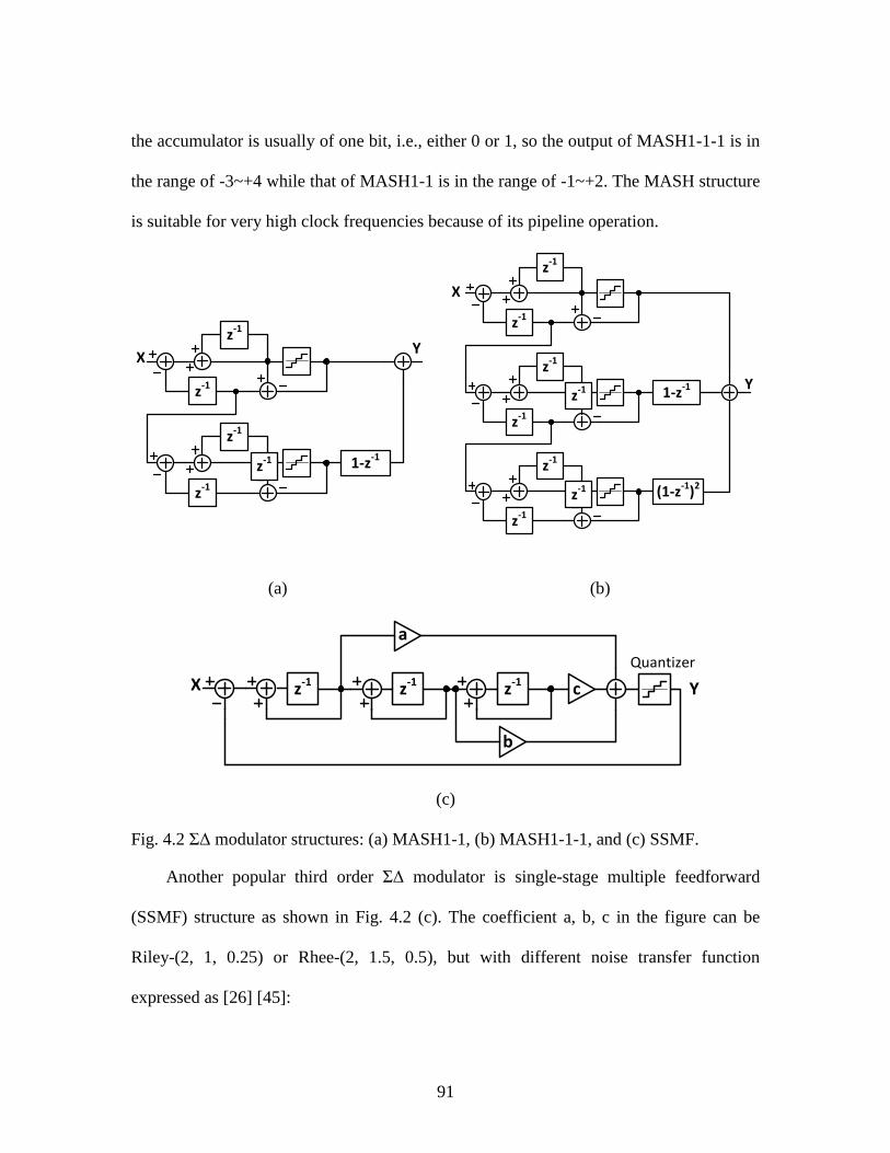
91
the accumulator is usually of one bit, i.e., either 0 or 1, so the output of MASH1-1-1 is in
the range of -3~+4 while that of MASH1-1 is in the range of -1~+2. The MASH structure
is suitable for very high clock frequencies because of its pipeline operation.
z-1
z-1
z-1
z-1
z-1 1-z-1
XY
z-1
z-1
z-1
z-1
z-1 1-z-1
X
Y
z-1
z-1
z-1 (1-z-1)2
(a) (b)
z-1 z-1 z-1
a
b
c YXQuantizer
(c)
Fig. 4.2 ΣΔ modulator structures: (a) MASH1-1, (b) MASH1-1-1, and (c) SSMF.
Another popular third order ΣΔ modulator is single-stage multiple feedforward
(SSMF) structure as shown in Fig. 4.2 (c). The coefficient a, b, c in the figure can be
Riley-(2, 1, 0.25) or Rhee-(2, 1.5, 0.5), but with different noise transfer function
expressed as [26] [45]:
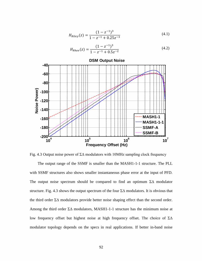
92
( ) ( )
(4.1)
( ) ( )
(4.2)
Fig. 4.3 Output noise power of ΣΔ modulators with 10MHz sampling clock frequency
The output range of the SSMF is smaller than the MASH1-1-1 structure. The PLL
with SSMF structures also shows smaller instantaneous phase error at the input of PFD.
The output noise spectrum should be compared to find an optimum ΣΔ modulator
structure. Fig. 4.3 shows the output spectrum of the four ΣΔ modulators. It is obvious that
the third order ΣΔ modulators provide better noise shaping effect than the second order.
Among the third order ΣΔ modulators, MASH1-1-1 structure has the minimum noise at
low frequency offset but highest noise at high frequency offset. The choice of ΣΔ
modulator topology depends on the specs in real applications. If better in-band noise
104
105
106
107
-200
-180
-160
-140
-120
-100
-80
-60
-40
Frequency Offset (Hz)
No
ise P
ow
er)
DSM Output Noise
MASH1-1
MASH1-1-1
SSMF-A
SSMF-B
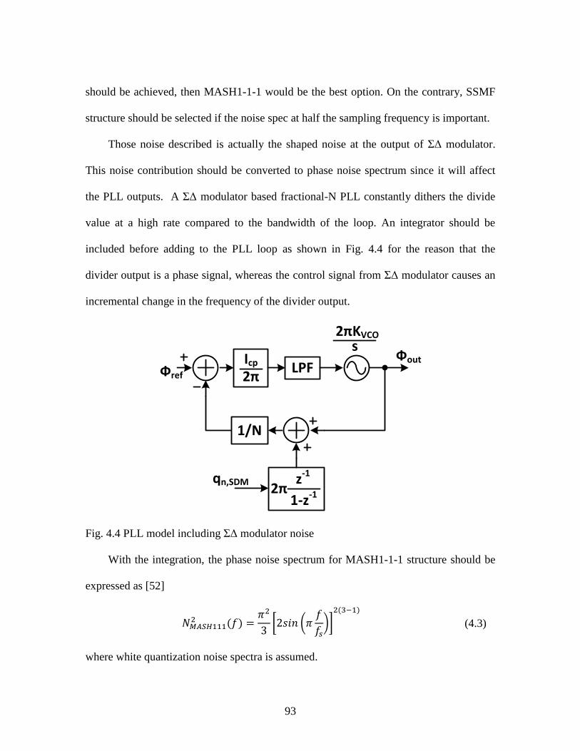
93
should be achieved, then MASH1-1-1 would be the best option. On the contrary, SSMF
structure should be selected if the noise spec at half the sampling frequency is important.
Those noise described is actually the shaped noise at the output of ΣΔ modulator.
This noise contribution should be converted to phase noise spectrum since it will affect
the PLL outputs. A ΣΔ modulator based fractional-N PLL constantly dithers the divide
value at a high rate compared to the bandwidth of the loop. An integrator should be
included before adding to the PLL loop as shown in Fig. 4.4 for the reason that the
divider output is a phase signal, whereas the control signal from ΣΔ modulator causes an
incremental change in the frequency of the divider output.
Icp 2π
LPF
2πKVCO s
1/N
Фref
z-1
1-z-1 2π
qn,SDM
Фout
Fig. 4.4 PLL model including ΣΔ modulator noise
With the integration, the phase noise spectrum for MASH1-1-1 structure should be
expressed as [52]
( )
[ (
*] ( )
(4.3)
where white quantization noise spectra is assumed.
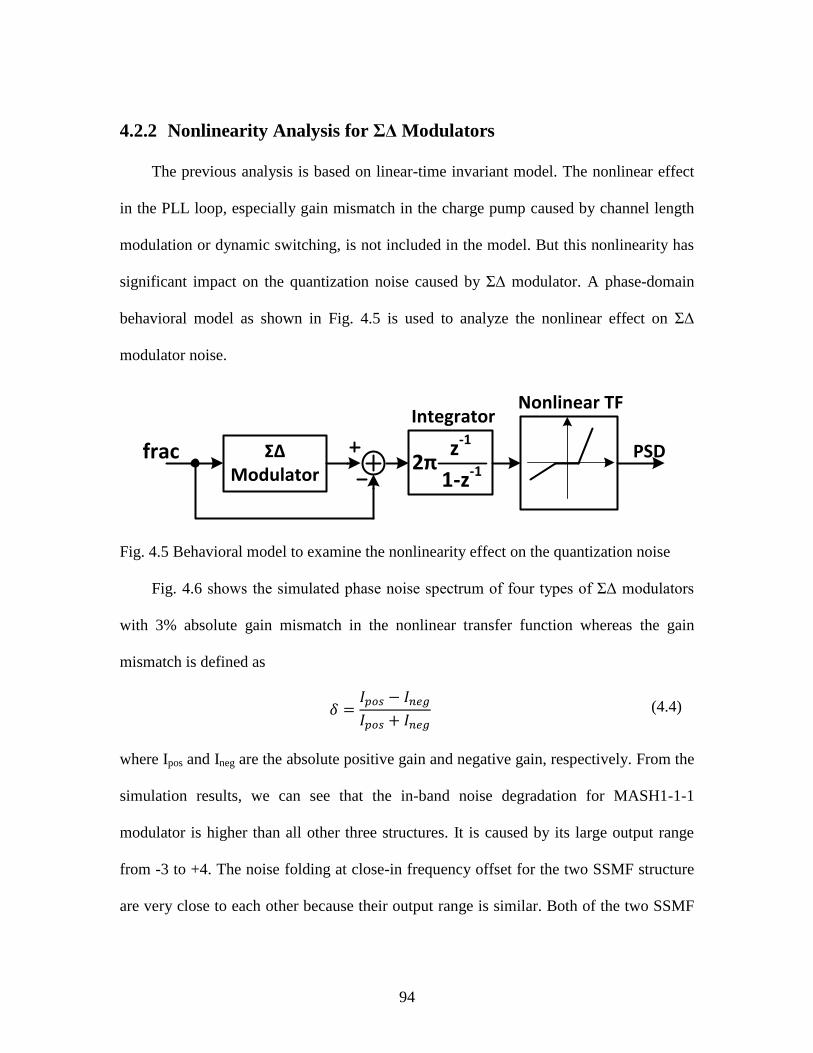
94
4.2.2 Nonlinearity Analysis for ΣΔ Modulators
The previous analysis is based on linear-time invariant model. The nonlinear effect
in the PLL loop, especially gain mismatch in the charge pump caused by channel length
modulation or dynamic switching, is not included in the model. But this nonlinearity has
significant impact on the quantization noise caused by ΣΔ modulator. A phase-domain
behavioral model as shown in Fig. 4.5 is used to analyze the nonlinear effect on ΣΔ
modulator noise.
ΣΔ Modulator
IntegratorNonlinear TF
PSDfrac z-1
1-z-1 2π
Fig. 4.5 Behavioral model to examine the nonlinearity effect on the quantization noise
Fig. 4.6 shows the simulated phase noise spectrum of four types of ΣΔ modulators
with 3% absolute gain mismatch in the nonlinear transfer function whereas the gain
mismatch is defined as
(4.4)
where Ipos and Ineg are the absolute positive gain and negative gain, respectively. From the
simulation results, we can see that the in-band noise degradation for MASH1-1-1
modulator is higher than all other three structures. It is caused by its large output range
from -3 to +4. The noise folding at close-in frequency offset for the two SSMF structure
are very close to each other because their output range is similar. Both of the two SSMF
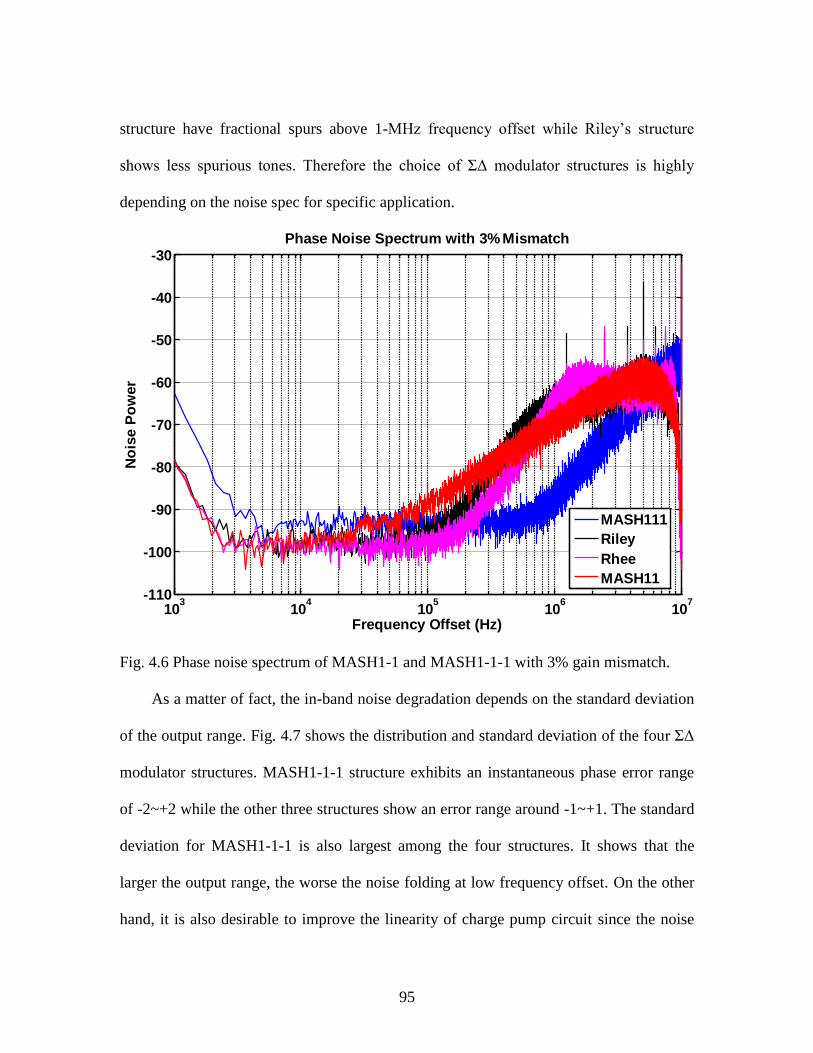
95
structure have fractional spurs above 1-MHz frequency offset while Riley’s structure
shows less spurious tones. Therefore the choice of ΣΔ modulator structures is highly
depending on the noise spec for specific application.
Fig. 4.6 Phase noise spectrum of MASH1-1 and MASH1-1-1 with 3% gain mismatch.
As a matter of fact, the in-band noise degradation depends on the standard deviation
of the output range. Fig. 4.7 shows the distribution and standard deviation of the four ΣΔ
modulator structures. MASH1-1-1 structure exhibits an instantaneous phase error range
of -2~+2 while the other three structures show an error range around -1~+1. The standard
deviation for MASH1-1-1 is also largest among the four structures. It shows that the
larger the output range, the worse the noise folding at low frequency offset. On the other
hand, it is also desirable to improve the linearity of charge pump circuit since the noise
103
104
105
106
107
-110
-100
-90
-80
-70
-60
-50
-40
-30
Frequency Offset (Hz)
No
ise P
ow
er
Phase Noise Spectrum with 3% Mismatch
MASH111
Riley
Rhee
MASH11
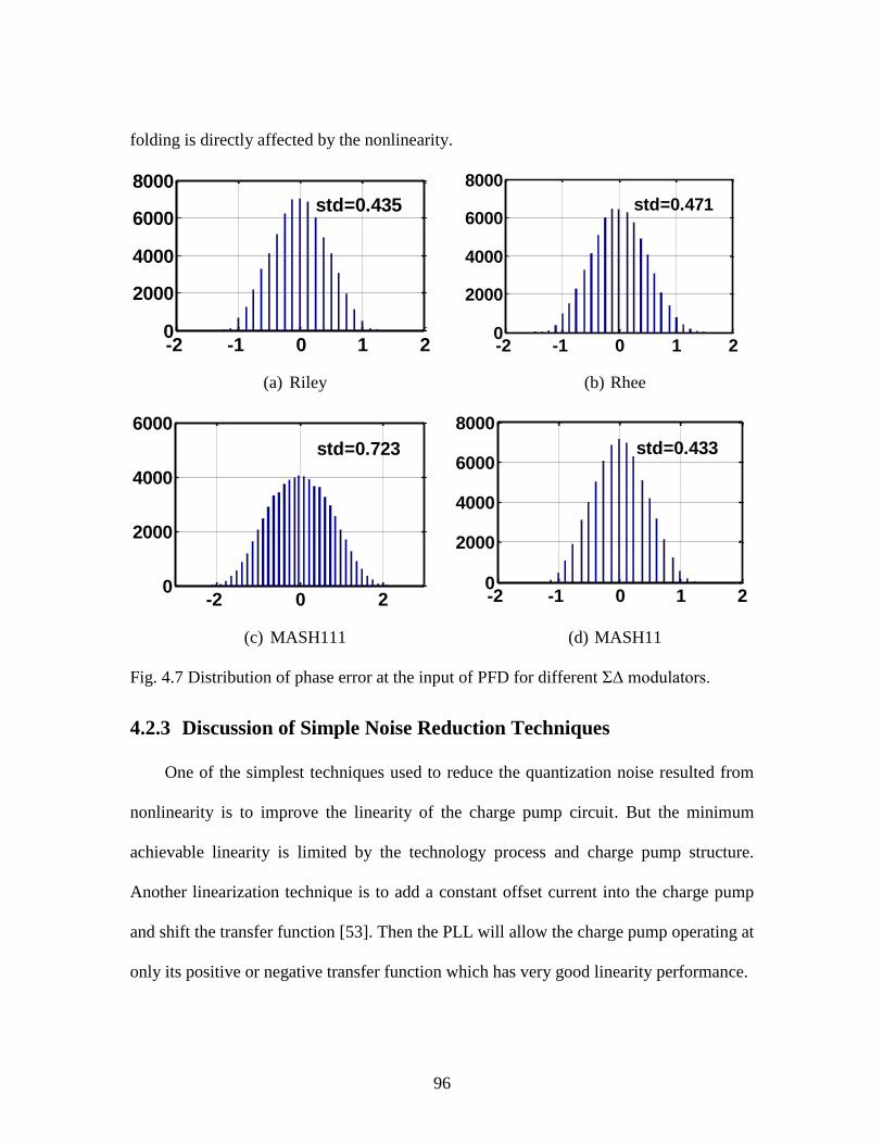
96
folding is directly affected by the nonlinearity.
(a) Riley (b) Rhee
(c) MASH111 (d) MASH11
Fig. 4.7 Distribution of phase error at the input of PFD for different ΣΔ modulators.
4.2.3 Discussion of Simple Noise Reduction Techniques
One of the simplest techniques used to reduce the quantization noise resulted from
nonlinearity is to improve the linearity of the charge pump circuit. But the minimum
achievable linearity is limited by the technology process and charge pump structure.
Another linearization technique is to add a constant offset current into the charge pump
and shift the transfer function [53]. Then the PLL will allow the charge pump operating at
only its positive or negative transfer function which has very good linearity performance.
-2 -1 0 1 20
2000
4000
6000
8000
std=0.435
-2 -1 0 1 20
2000
4000
6000
8000
std=0.471
-2 0 20
2000
4000
6000
std=0.723
-2 -1 0 1 20
2000
4000
6000
8000
std=0.433
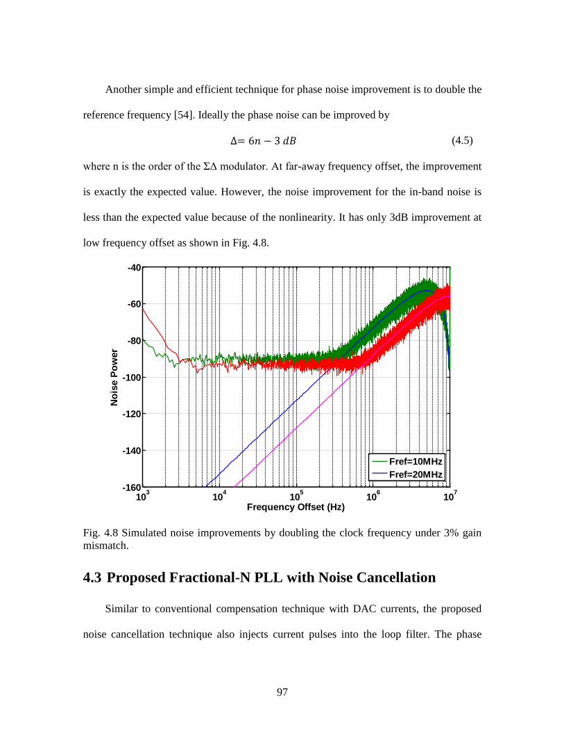
97
Another simple and efficient technique for phase noise improvement is to double the
reference frequency [54]. Ideally the phase noise can be improved by
(4.5)
where n is the order of the ΣΔ modulator. At far-away frequency offset, the improvement
is exactly the expected value. However, the noise improvement for the in-band noise is
less than the expected value because of the nonlinearity. It has only 3dB improvement at
low frequency offset as shown in Fig. 4.8.
Fig. 4.8 Simulated noise improvements by doubling the clock frequency under 3% gain
mismatch.
4.3 Proposed Fractional-N PLL with Noise Cancellation
Similar to conventional compensation technique with DAC currents, the proposed
noise cancellation technique also injects current pulses into the loop filter. The phase
103
104
105
106
107
-160
-140
-120
-100
-80
-60
-40
Frequency Offset (Hz)
No
ise P
ow
er
Fref=10MHz
Fref=20MHz
98
error can be compensated in three ways: a) pulse-width modulated (PWM) current pulses;
b) pulse-amplitude modulated (PAM) current pulses; c) combination of PWM and PAM.
The conventional fractional-N PLL can be modified by adding only small cost of
digital control logic to implement the noise compensation technique. Typically a multi-
modulus divider is using to divide the VCO signal to reference frequency. The divider in
the fractional-N PLL will up or down count N cycle of VCO period to implement N-
divider. This feature can be used to produce PWM current. With an auxiliary counter, a
current pulse with X VCO cycles can be injected into the loop filter and compensate the
instantaneous phase error. The main limitation for this technique is that X should be
smaller than the division ratio of N. Furthermore, the in-band noise at PLL output may
increase because the long turn-on time of the DAC current injects more thermal noise.
Another technique using PAM current pulses can be implemented by current DAC.
This technique is useful for fractional-N PLL with phase error in the range of 0~1 VCO
periods. However, it requires large area of current DAC circuit to compensate phase error
in the range of -2~2 VCO periods for high-order ΣΔ modulators. Therefore, a
compensating circuit that can generate both positive and negative phase error should be
applied to cancel the quantization noise.
Fig. 4.9 (a) shows the system diagram of the proposed fractional-N PLL using the
combination of PAM and PWM current pulses for high-order ΣΔ noise cancellation. The
charge pump produces PAM signal while the PWM signal is produced by the pulse
generation module. The PFD block, as shown in Fig. 4.9 (b), produces up and down
control signal for the switches in the charge pump.
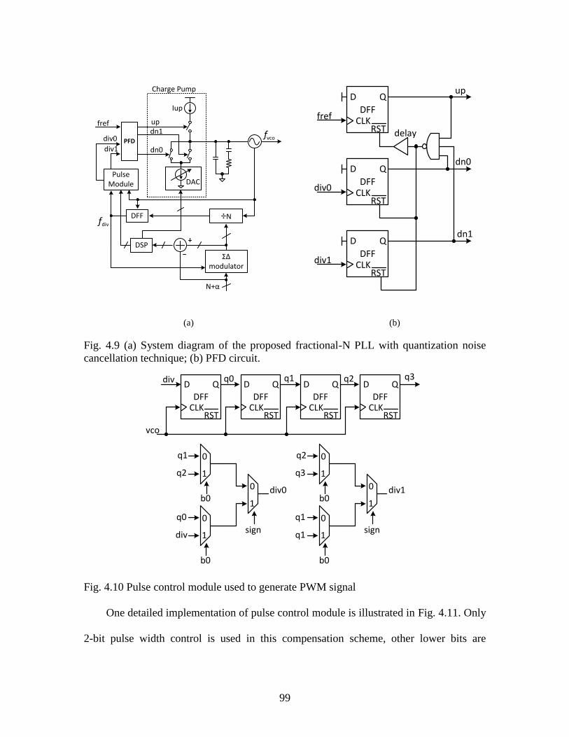
99
updn1
PFD
fref
÷N
ΣΔ modulator
DSP
fvco
fdiv
N+α
Iup
DAC
dn0
DFF
Charge Pump
Pulse Module
div0
div1
DFF
D
CLKRST
Q
DFF
D
CLKRST
Q
DFF
D
CLKRST
Q
fref
div0
div1
delay
up
dn0
dn1
(a) (b)
Fig. 4.9 (a) System diagram of the proposed fractional-N PLL with quantization noise
cancellation technique; (b) PFD circuit.
DFF
D
CLKRST
Q
DFF
D
CLKRST
Q
DFF
D
CLKRST
Q
DFF
D
CLKRST
Q
0
1
0
1
div
vco
q0 q1 q2 q3
div
q0
q1
sign
b0
div0
0
1q2
b00
1
0
1q1
q1
q2
sign
b0
div1
0
1q3
b0
Fig. 4.10 Pulse control module used to generate PWM signal
One detailed implementation of pulse control module is illustrated in Fig. 4.11. Only
2-bit pulse width control is used in this compensation scheme, other lower bits are
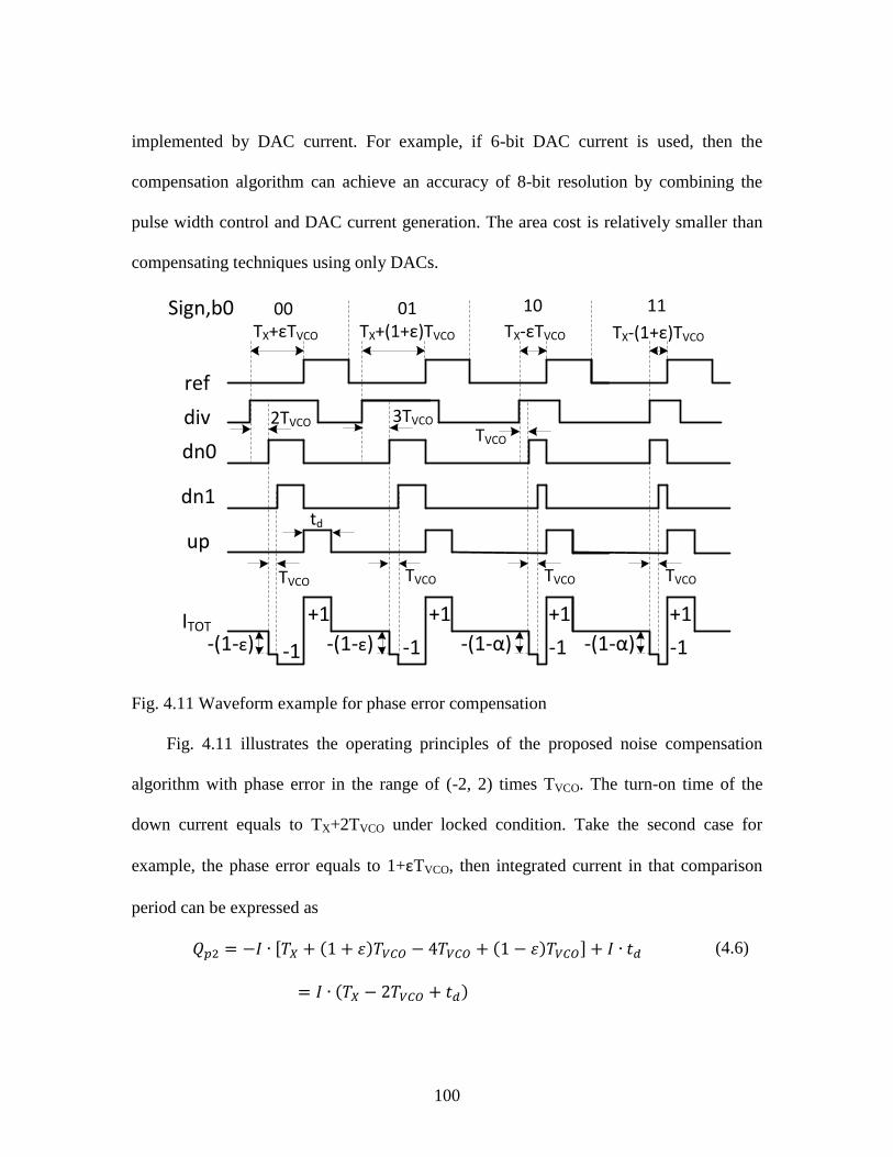
100
implemented by DAC current. For example, if 6-bit DAC current is used, then the
compensation algorithm can achieve an accuracy of 8-bit resolution by combining the
pulse width control and DAC current generation. The area cost is relatively smaller than
compensating techniques using only DACs.
ref
dn0
dn1
up
ITOT+1
TVCO TVCO
td
TVCO
TX+εTVCO
-(1-ε) -(1-ε)
+1 +1
-1 -1 -1
div
TX+(1+ε)TVCO TX-εTVCO
2TVCO 3TVCO
TVCO
TVCO
+1
-1
TX-(1+ε)TVCO
00 01Sign,b0 10 11
-(1-α) -(1-α)
Fig. 4.11 Waveform example for phase error compensation
Fig. 4.11 illustrates the operating principles of the proposed noise compensation
algorithm with phase error in the range of (-2, 2) times TVCO. The turn-on time of the
down current equals to TX+2TVCO under locked condition. Take the second case for
example, the phase error equals to 1+εTVCO, then integrated current in that comparison
period can be expressed as
[ ( ) ( ) ]
( )
(4.6)
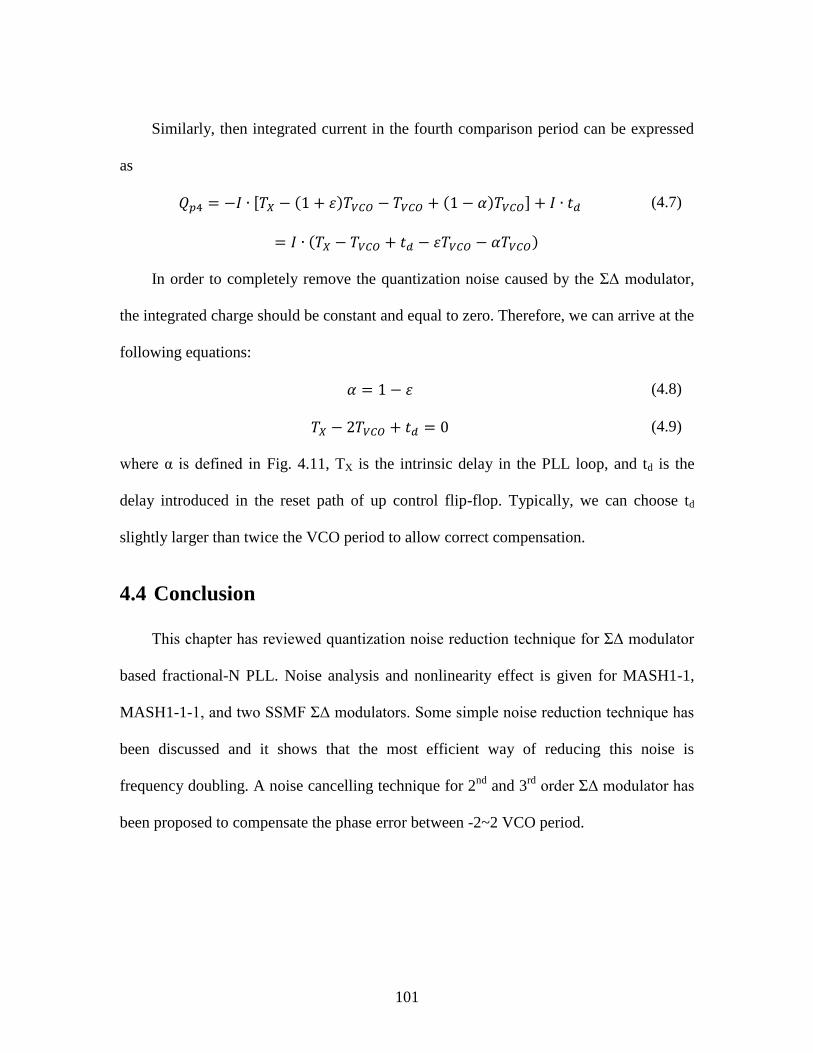
101
Similarly, then integrated current in the fourth comparison period can be expressed
as
[ ( ) ( ) ]
( )
(4.7)
In order to completely remove the quantization noise caused by the ΣΔ modulator,
the integrated charge should be constant and equal to zero. Therefore, we can arrive at the
following equations:
(4.8)
(4.9)
where α is defined in Fig. 4.11, TX is the intrinsic delay in the PLL loop, and td is the
delay introduced in the reset path of up control flip-flop. Typically, we can choose td
slightly larger than twice the VCO period to allow correct compensation.
4.4 Conclusion
This chapter has reviewed quantization noise reduction technique for ΣΔ modulator
based fractional-N PLL. Noise analysis and nonlinearity effect is given for MASH1-1,
MASH1-1-1, and two SSMF ΣΔ modulators. Some simple noise reduction technique has
been discussed and it shows that the most efficient way of reducing this noise is
frequency doubling. A noise cancelling technique for 2nd
and 3rd
order ΣΔ modulator has
been proposed to compensate the phase error between -2~2 VCO period.
102
5.1 Introduction
With the improvements in semiconductor process, low-cost consumer applications
for radar transceiver have been proposed, such as automotive collision avoidance, cruise
control, and fluid-level indicators. High performance local oscillator (LO) signals with
clean spectrum are required to down-convert the received signal and up-convert the base-
band signal to radio-frequency (RF) signal for radar transceiver. PLL is such a system
that can be used to generate LO signals with large frequency range by tuning the integer
or fractional division ratio. This chapter presents an integer-N PLL system comprised of a
wide-band VCO, divider-by-two circuit (DTC), multi-modulus divider (MMD), phase-
frequency detector (PFD) and charge pump (CP) in current-mode logic (CML) type, and
divider modules for mixers and direct digital synthesis (DDS) clock.
Among the building blocks of PLL system, VCO plays a key role in generating a
clean spectrum since it dominates the out-of-band phase noise performance. Recently, a
tail current shaping technique has been proposed to improve the phase noise of CMOS
VCOs [55]. Similarly, the current shaping technique can also be used to decrease the
noise performance of bipolar VCOs. With the filtering capacitor at the current tail, the
VCO phase noise can be improved by 3.5dB according to the simulation results. Usually,
the phase noise performance of a VCO is better with smaller VCO tuning gain. In order
Chapter 5 A Wide-Band Integer-N PLL Design
103
to improve the phase noise and cover large frequency tuning range, the overall frequency
range can be divided into 16 or more sub-bands controlled by numbers of MOS switches
[56]. However the utilization of MOS switches will increase the parasitic capacitance to
the VCO load and thus narrow the frequency tuning range. To address this problem, static
bias voltage is applied to those parasitic diodes.
A frequency divider is a critical building block in high-performance clock
synthesizers. In order to divide the high-frequency VCO output, the divider speed and
power trade-off should be carefully considered at an early design phase. Minimum power
consumption for CMOS dividers based on CML can be achieved by choosing the
optimum transistor size and operating point [57]. However, in real applications, it is not
intuitive to use such a design methodology for divider design.
Usually a divider circuit has a self-oscillation frequency Fosc which requires
minimum input power to divide the input signal [58]. To find Fosc, the frequency at
which the DTC and divide-by-2/3 cell resonate, a simplified design technique based on
timing delay analysis is proposed. With the proposed optimization technique, the CML
divider chain can achieve minimum power consumption in either CMOS or bipolar
technology. After the minimum input power at Fosc of dividers is found, the signal swing
should be kept large enough to tolerate process, voltage, and temperature (PVT)
variation. Besides, the input signal swing should also be kept large to improve the phase
noise performance of the divider. To accomplish optimum divider design, it is desirable
to make clear trade-off between the phase noise, power and speed.
The proposed PLL architecture is shown in Fig. 5.1. The output signal of the VCO is
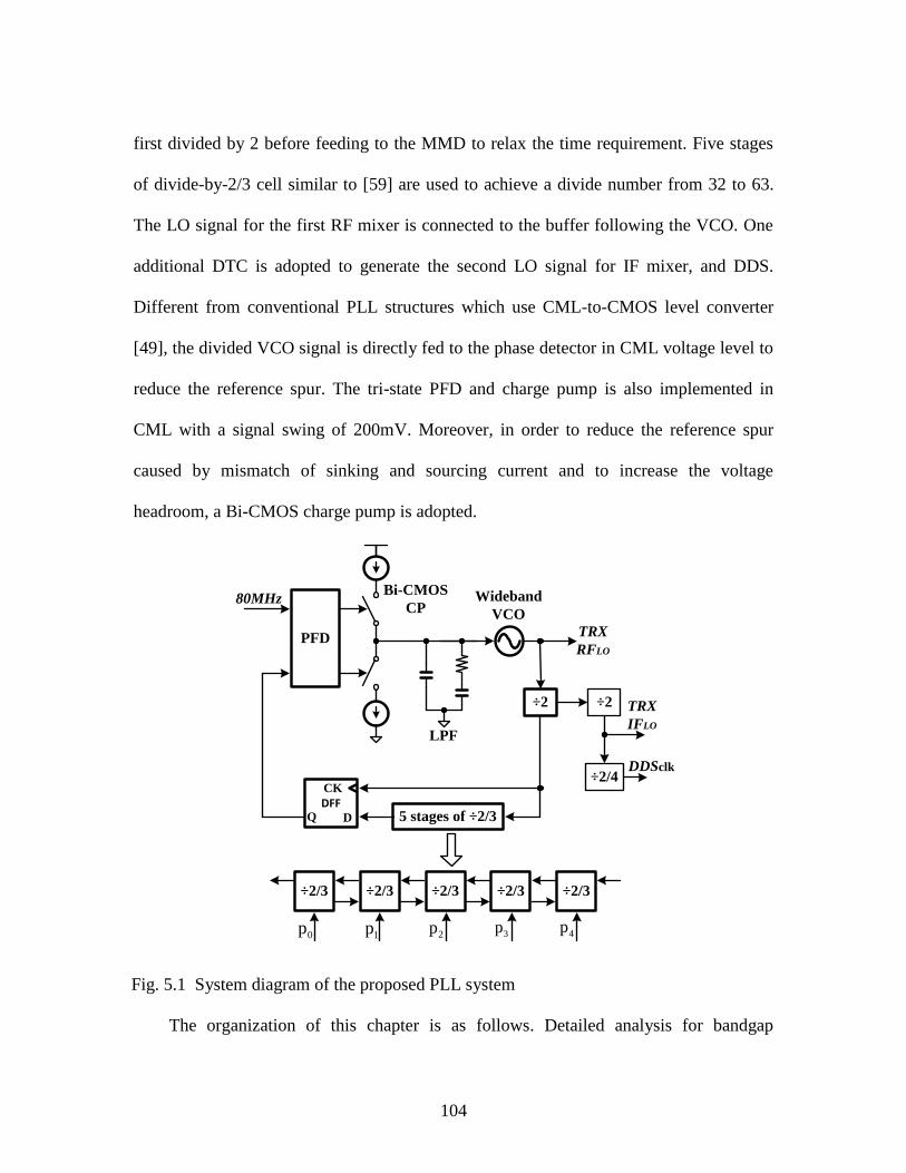
104
first divided by 2 before feeding to the MMD to relax the time requirement. Five stages
of divide-by-2/3 cell similar to [59] are used to achieve a divide number from 32 to 63.
The LO signal for the first RF mixer is connected to the buffer following the VCO. One
additional DTC is adopted to generate the second LO signal for IF mixer, and DDS.
Different from conventional PLL structures which use CML-to-CMOS level converter
[49], the divided VCO signal is directly fed to the phase detector in CML voltage level to
reduce the reference spur. The tri-state PFD and charge pump is also implemented in
CML with a signal swing of 200mV. Moreover, in order to reduce the reference spur
caused by mismatch of sinking and sourcing current and to increase the voltage
headroom, a Bi-CMOS charge pump is adopted.
Wideband
VCO
TRX
RFLO
PFD
80MHz
÷2 ÷2
Bi-CMOS
CP
÷2/4
TRX
IFLO
DDSclk
÷2/3 ÷2/3 ÷2/3 ÷2/3 ÷2/3
5 stages of ÷2/3DFF
D
CK
Q
4p3p
2p1p0p
LPF
Fig. 5.1 System diagram of the proposed PLL system
The organization of this chapter is as follows. Detailed analysis for bandgap
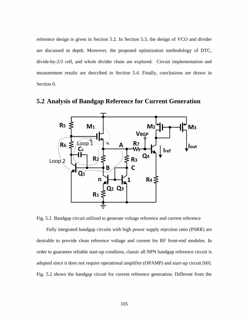
105
reference design is given in Section 5.2. In Section 5.3, the design of VCO and divider
are discussed in depth. Moreover, the proposed optimization methodology of DTC,
divide-by-2/3 cell, and whole divider chain are explored. Circuit implementation and
measurement results are described in Section 5.4. Finally, conclusions are drawn in
Section 0.
5.2 Analysis of Bandgap Reference for Current Generation
M2 M3
Q3Q2
Q1
Q4
M1
R1
R2 R3
R4
R6
R5
VBGP
A
B
n 1
Iref
C
CcIout
R7
Loop 2
Loop 1
Fig. 5.2 Bandgap circuit utilized to generate voltage reference and current reference
Fully integrated bandgap circuits with high power supply rejection ratio (PSRR) are
desirable to provide clean reference voltage and current for RF front-end modules. In
order to guarantee reliable start-up condition, classic all NPN bandgap reference circuit is
adopted since it does not require operational amplifier (OPAMP) and start-up circuit [60].
Fig. 5.2 shows the bandgap circuit for current reference generation. Different from the
106
classic structure, a NMOS transistor with small threshold voltage is used to enhance the
PSRR. The voltage at node A shown in Fig. 5.2 is
( ) ( ) (5.1)
The voltage difference of VBE2 and VBE3 produce a current following through
resistor R1 expressed as
(
*
(
* (5.2)
Supposing the current gain β is very large and Q1, Q3 have the same size, the voltage
at base of Q1 and Q2 will be close because of the negative feedback loop formed by Q1,
R5, and M1. With VBE1=VBE3, we can obtain the following equation
⇒
(5.3)
Then the bandgap voltage at node A can be written as
(
* (5.4)
Note that there is a positive feedback loop 2 in the circuit. To stabilize the circuit, it
is necessary to maintain the positive loop gain smaller than the negative loop gain.
Assuming that β is very large, we have the following condition for stable operation:
(5.5)
The PSRR under dc condition can be derived and approximated as
( )
(5.6)
In order to improve the PSRR, we need to increase the resistor value of R5; however,
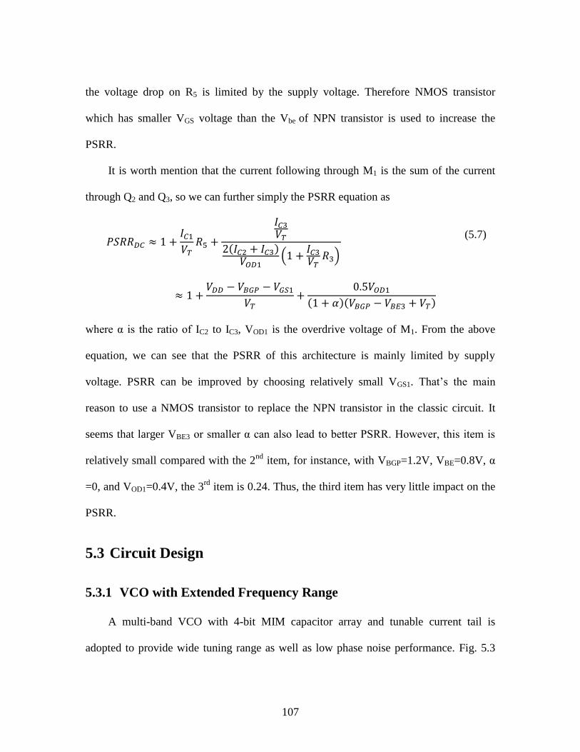
107
the voltage drop on R5 is limited by the supply voltage. Therefore NMOS transistor
which has smaller VGS voltage than the Vbe of NPN transistor is used to increase the
PSRR.
It is worth mention that the current following through M1 is the sum of the current
through Q2 and Q3, so we can further simply the PSRR equation as
( )
( )
( )( )
(5.7)
where α is the ratio of IC2 to IC3, VOD1 is the overdrive voltage of M1. From the above
equation, we can see that the PSRR of this architecture is mainly limited by supply
voltage. PSRR can be improved by choosing relatively small VGS1. That’s the main
reason to use a NMOS transistor to replace the NPN transistor in the classic circuit. It
seems that larger VBE3 or smaller α can also lead to better PSRR. However, this item is
relatively small compared with the 2nd
item, for instance, with VBGP=1.2V, VBE=0.8V, α
=0, and VOD1=0.4V, the 3rd
item is 0.24. Thus, the third item has very little impact on the
PSRR.
5.3 Circuit Design
5.3.1 VCO with Extended Frequency Range
A multi-band VCO with 4-bit MIM capacitor array and tunable current tail is
adopted to provide wide tuning range as well as low phase noise performance. Fig. 5.3
108
presents the proposed bipolar NPN cross-coupled VCO.
vtune
vb
b0b1b2b3
bi
bi
Parasitic
diode...
vb1
Cfilt
Cc Cc
Cb Cb
Fig. 5.3 Schematic of the proposed VCO with extended tuning range
A symmetric inductor with deep trench is used to provide better isolation from noise
coupling from substrate. Conventional switches used for coarse tuning between different
VCO bands consist of three NMOS transistors [56]. However, parasitic capacitances
resulted from parasitic drain (n+)-to-substrate (p+) diodes vary with the dc voltage
applied to its drain, i.e. the smaller the dc voltage, the larger the parasitic capacitance.
When the NMOS transistors are off, the drain of the NMOS switch would be floating and
close to zero and thus large parasitic capacitance loads the LC tank. Moreover, to
decrease the series resistor and increase the quality factor of the capacitor array, the
NMOS transistors for switches are usually realized with large dimensions. Then the large
tuning range is suffered from these parasitic drain-substrate diodes. In order to widen the
VCO frequency tuning range, when the NMOS switches are off, a dc voltage equal to
109
supply voltage is applied to the drain through small PMOS transistors as shown in Fig.
5.3. With the proposed frequency extending technique, the simulated frequency tuning
range can be increased from 2.32GHz to 2.74GHz, which is 18% improvement. A noise
filtering MIM capacitor is used to reduce the noise up-conversion from the current tail
and the simulated improvement is 3.5dB.
The bipolar transistor can be easily broken down with a 2.0-2.2V supply voltage
since its collector-emitter break down voltage Vceo is 1.6 Volts. In order to avoid break
down, the bias voltage vb as shown in Fig. 5.3 should be large. However, large vb will
force the bipolar transistor into saturation region which is not desirable since the VCO
phase noise will be degraded in this operating region. The following equations should be
met to maintain the largest signal swing for best phase noise performance and avoid
break down:
( )
( ) (5.8)
where voltage divider ratio ( ) is introduced to alleviate the requirement
of breakdown voltage. Avco is the single-ended VCO signal amplitude. Vmargin=0.2V and
Vth=0.5V are the voltage margin from saturation and threshold voltage of bipolar
transistor, respectively. According to the noise equation (66) of bipolar cross-coupled
differential LC-tank VCO in reference [61], we know that the larger the voltage divider
ratio n, the better the phase noise. To prevent break down, n=2/3 is chosen and the
corresponding maximum differential signal amplitude is 0.54V.
5.3.2 Power and Speed Optimization for DTC
110
R R
T1 T2 T3 T4
T9 T10
IB
R R
T5 T6 T7 T8
T11 T12
IB
op1 on1 op2 on2
op1on1on2 op2
ckin
vb
C C C C
Latch1 Latch2
iop2 ion2iop1 ion1
(a)
(b)
Fig. 5.4 Divide-by-2 circuit: (a) Circuit schematic and (b) simplified waveforms for
derivation of self-oscillation frequency
Conventional CML structure is used to implement the DTC and divide-by-2/3 cell.
Fig. 5.4 shows the DTC schematic and output waveforms under self-oscillation mode.
Analytic design equation of Fosc will be developed to achieve the optimum performance.
0 1 2 3 4 5 6 7 80
0.2
0.4
0.6
0.8
1Waveforms of Divide-by-2 Circuit
Time
Norm
aliz
ed V
oltage
0 1 2 3 4 5 6 7 80
0.1
0.2
0.3
0.4
0.5
0.6
0.7
0.8
0.9
1
0 1 2 3 4 5 6 7 80
0.2
0.4
0.6
0.8
1
Norm
aliz
ed C
urr
ent
Von
VopIonIop
T
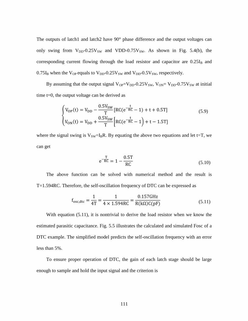
111
The outputs of latch1 and latch2 have 90° phase difference and the output voltages can
only swing from VDD-0.25VSW and VDD-0.75VSW. As shown in Fig. 5.4(b), the
corresponding current flowing through the load resistor and capacitor are 0.25IB and
0.75IB when the VOP equals to VDD-0.25VSW and VDD-0.5VSW, respectively.
By assuming that the output signal VOP=VDD-0.25VSW, VON= VDD-0.75VSW at initial
time t=0, the output voltage can be derived as
( )
[ ( ) ]
( )
[ ( * ]
(5.9)
where the signal swing is VSW=IBR. By equating the above two equations and let t=T, we
can get
(5.10)
The above function can be solved with numerical method and the result is
T=1.594RC. Therefore, the self-oscillation frequency of DTC can be expressed as
( ) ( ) (5.11)
With equation (5.11), it is nontrivial to derive the load resistor when we know the
estimated parasitic capacitance. Fig. 5.5 illustrates the calculated and simulated Fosc of a
DTC example. The simplified model predicts the self-oscillation frequency with an error
less than 5%.
To ensure proper operation of DTC, the gain of each latch stage should be large
enough to sample and hold the input signal and the criterion is
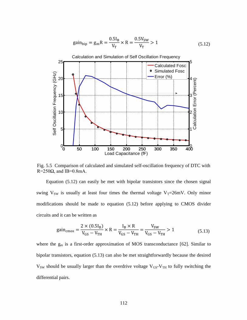
112
(5.12)
Fig. 5.5 Comparison of calculated and simulated self-oscillation frequency of DTC with
R=250Ω, and IB=0.8mA.
Equation (5.12) can easily be met with bipolar transistors since the chosen signal
swing VSW is usually at least four times the thermal voltage VT=26mV. Only minor
modifications should be made to equation (5.12) before applying to CMOS divider
circuits and it can be written as
( )
(5.13)
where the gm is a first-order approximation of MOS transconductance [62]. Similar to
bipolar transistors, equation (5.13) can also be met straightforwardly because the desired
VSW should be usually larger than the overdrive voltage VGS-VTH to fully switching the
differential pairs.
0 50 100 150 200 250 300 350 4000
5
10
15
20
25Calculation and Simulation of Self Oscillation Frequency
Load Capacitance (fF)
Se
lf O
scill
atio
n F
req
ue
ncy (
GH
z)
0 50 100 150 200 250 300 350 4000
1
2
3
4
5
Ca
lcu
latio
n E
rro
r (P
erc
en
t)
Calculated Fosc
Simulated Fosc
Error (%)
113
Fig. 5.6 Simulated sensitivity curves of the DTC with R=250 Ω, C=130fF and phase
noise performance with different input signal
Fig. 5.6 shows the sensitivity curves of the DTC at 3 different bias condition and
phase noise variation with input signal. The simulated Fosc is around 9.3/2=4.65GHz and
the calculation result is 4.83GHz which is 3.9% higher than that of simulation. On the
other hand, since the phase noise performance of DTC depends on the input power, as
shown in Fig. 5.6, the input signal should be large enough to avoid phase noise
degradation.
5.3.3 Design Divide-by-2/3 and MMD
The other main building blocks for MMD is the divide-by-2/3 cell as shown in Fig.
5.7, which is made up of two groups of components: (1) gate G1, latches DL1 and DL2
for divide-by-2/3; (2) gate G2 and G3, latches DL3 and DL4 for divide-by-3 only. The
0 2 4 6 8 10 12 14 16 18 200
20
40
60
80
100
120
140
160
Input Frequency (GHz)
Diffe
rential In
put A
mplit
ude (
mV
)
IB=0.8mA
IB=0.6mA
IB=1.0mA
0 20 40 60 80 100 120 140 160
-160
-155
-150
-145
-140
-135
-130
-125
-120
Vin (mV)
Phase N
ois
e @
1M
Hz O
ffset (d
Bc/H
z)
Fin=7GHz
Fin=9GHz
Fin=12GHz
Sensitivity Curve of DTC
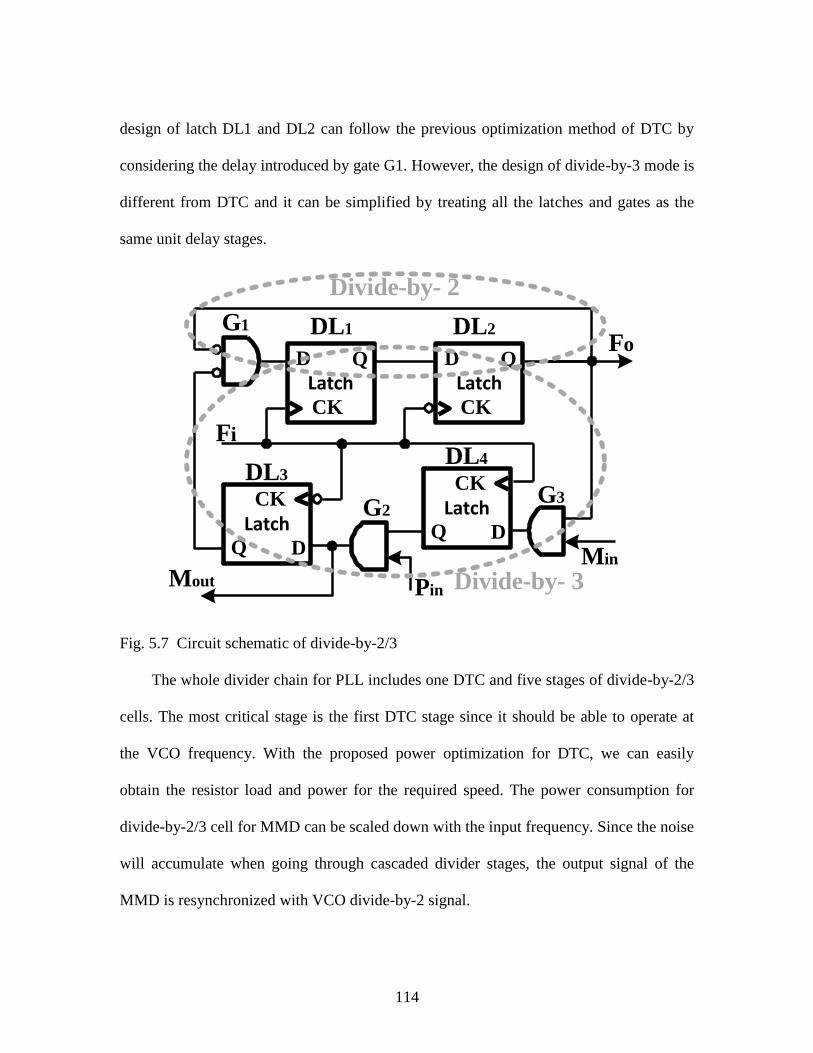
114
design of latch DL1 and DL2 can follow the previous optimization method of DTC by
considering the delay introduced by gate G1. However, the design of divide-by-3 mode is
different from DTC and it can be simplified by treating all the latches and gates as the
same unit delay stages.
LatchD
CK
Q
LatchD
CK
Q
LatchD
CK
QLatchD
CK
Q
Fo
Fi
Pin
Min
Mout
DL1 DL2G1
G2G3
DL3DL4
Divide-by- 2
Divide-by- 3
Fig. 5.7 Circuit schematic of divide-by-2/3
The whole divider chain for PLL includes one DTC and five stages of divide-by-2/3
cells. The most critical stage is the first DTC stage since it should be able to operate at
the VCO frequency. With the proposed power optimization for DTC, we can easily
obtain the resistor load and power for the required speed. The power consumption for
divide-by-2/3 cell for MMD can be scaled down with the input frequency. Since the noise
will accumulate when going through cascaded divider stages, the output signal of the
MMD is resynchronized with VCO divide-by-2 signal.
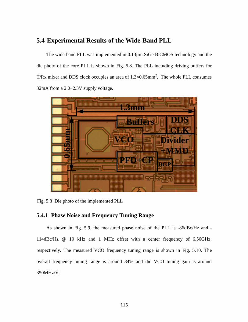
115
5.4 Experimental Results of the Wide-Band PLL
The wide-band PLL was implemented in 0.13 m SiGe BiCMOS technology and the
die photo of the core PLL is shown in Fig. 5.8. The PLL including driving buffers for
T/Rx mixer and DDS clock occupies an area of 1.3×0.65mm2. The whole PLL consumes
32mA from a 2.0~2.3V supply voltage.
Fig. 5.8 Die photo of the implemented PLL
5.4.1 Phase Noise and Frequency Tuning Range
As shown in Fig. 5.9, the measured phase noise of the PLL is -86dBc/Hz and -
114dBc/Hz @ 10 kHz and 1 MHz offset with a center frequency of 6.56GHz,
respectively. The measured VCO frequency tuning range is shown in Fig. 5.10. The
overall frequency tuning range is around 34% and the VCO tuning gain is around
350MHz/V.
VCO
Buffers DDS
CLK
PFD+CP
Divider
+MMD
BGP
1.3mm
0.6
5m
m
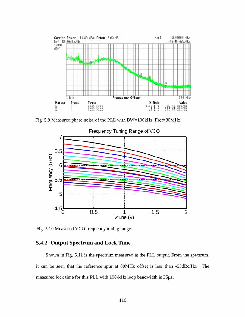
116
Fig. 5.9 Measured phase noise of the PLL with BW=100kHz, Fref=80MHz
Fig. 5.10 Measured VCO frequency tuning range
5.4.2 Output Spectrum and Lock Time
Shown in Fig. 5.11 is the spectrum measured at the PLL output. From the spectrum,
it can be seen that the reference spur at 80MHz offset is less than -65dBc/Hz. The
measured lock time for this PLL with 100-kHz loop bandwidth is 35µs.
0 0.5 1 1.5 24.5
5
5.5
6
6.5
7Frequency Tuning Range of VCO
Vtune (V)
Fre
quency (
GH
z)
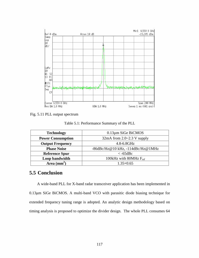
117
Fig. 5.11 PLL output spectrum
Table 5.1: Performance Summary of the PLL
Technology 0.13µm SiGe BiCMOS
Power Consumption 32mA from 2.0~2.3 V supply
Output Frequency 4.8-6.8GHz
Phase Noise -86dBc/Hz@10 kHz, -114dBc/Hz@1MHz
Reference Spur < -65dBc
Loop bandwidth 100kHz with 80MHz Fref
Area (mm2) 1.35×0.65
5.5 Conclusion
A wide-band PLL for X-band radar transceiver application has been implemented in
0.13 m SiGe BiCMOS. A multi-band VCO with parasitic diode biasing technique for
extended frequency tuning range is adopted. An analytic design methodology based on
timing analysis is proposed to optimize the divider design. The whole PLL consumes 64
118
mW power from a 2.0 V supply and occupies a core area of 0.88 mm2. The performance
summary for the PLL frequency synthesizer is given in Table 5.1.
119
6.1 Summary of the Works
This dissertation presents capacitive-coupling QVCOs with improved phase noise
performance and elimination of bi-modal oscillation. A key contribution of this work was
the capacitive coupling technique for quadrature generation which is free from the
problem of the noise degradation in the quadrature-coupling path and phase ambiguity.
Meantime, it shows noise improvement over its single-phase counterpart. Theoretical
analysis, combined with simulation and experimental results is given to show the
efficiency of the proposed quadrature-coupling technique.
Two QVCOs with different architectures have been implemented in 0.13µm CMOS
technology. A 0.6-V differential Colpitts QVCO with capacitive-coupling technique and
enhanced swing has been optimized to achieve minimum phase noise performance. The
capacitive-coupling ratio can be chosen for either better phase noise or phase error
performance to meet specs for different applications. Different from classic QVCOs
using active parallel coupling technique, the capacitive coupling provides better phase
noise performance due to its improved ISF. A secondary inductor is inserted at the
bottom to enhance the output signal swing, allowing improved phase noise performance
at very low supply voltage.
For the most popular commercial applications, QVCO with well-controlled current
Chapter 6 Summary and Future Work
120
bias is preferred due to its advantage of simple structure and high reliability. Another
QVCO structure with capacitive-coupling is introduced to provide robust solution for
such applications. This CC-QVCO shows excellent phase noise tolerance and phase error
over wide frequency tuning range. Silicon implementation and measurement are given to
verify the proposed quadrature-coupling technique. The reliability of the proposed CC-
QVCO has been proved from the comparison with class-C mode TS-QVCO whose
published phase noise performance is among the top.
Another major contribution of this work is the quantization noise suppressing
technique and model for noise folding resulted from nonlinearity in a fractional-N PLL.
Several techniques for phase noise reduction have been discussed and a noise reduction
technique for higher order SDM is proposed. Moreover, a noise behavioral model
including the charge pump nonlinearity is developed for fractional-N PLL.
The final major contribution of this dissertation is a wide-band integer-N PLL for
wireless transceiver design. Detailed theoretical analysis of a Bi-CMOS bandgap is given
to show the improved PSRR over its conventional counterpart who uses bipolar transistor
only. Simple design methodology for power optimization of dividers has been proved
with simulation results.
6.2 Future Work
The proposed capacitive coupling technique is very suitable to implement a
quadrature oscillator with improved phase noise performance. The phase delay
introduced to avoid phase ambiguity is around 40° for the 0.6-V Colpitts QVCO and hard
121
to control, especially at frequencies above 10GHz because of the short time period. One
future direction might be to develop phase delaying generation technique that suitable for
frequency above 10GHz applications. Moreover, the capacitive coupling technique is also
suitable for multi-phase oscillator, such as three or four phase. Another promising
direction might be to develop multi-phase VCO with the proposed capacitive-coupling
technique for phase array transceivers due to its promising feature of noise reduction.
The proposed quantization noise reduction technique is useful and efficient. But
further system level simulation and circuit design is not included. Therefore, one possible
future work is to design a fractional-N PLL with artificially introduced nonlinearity and
then verify the model through silicon verification.
122
Bibliography
[1] J. Yu, F. Zhao, J. Cali, D. Ma, X. Geng, F. F. Dai, J. D. Irwin, A. Aklian, “A single-
chip X-band chirp radar MMIC with stretch processing,” in Proc. IEEE Custom
Integr. Circuits Conf., Sep. 2012, pp. 1-4.
[2] S. L. J. Gierkink,S. Levantino, R. C. Frye, C. Samori, and V. Boccuzzi, “A low
phase-noise 5-GHz CMOS quadrature VCO using superharmonic coupling,” IEEE
J. Solid-State Circuits, vol. 38, no. 7, pp. 1148–1154, Jul. 2003.
[3] X. Li, S. shekhar, and D. J. Allstot, “Gm-boosted common-gate LNA and differential
Colpitts VCO/QVCO in 0.18-μm CMOS,” IEEE J. Solid-State Circuits, vol. 40, no.
12, pp. 2609–2619, Dec. 2005.
[4] J. Crols and M. Steyaert, “A fully integrated 900 MHz CMOS double quadrature
downconverter,” in IEEE Int. Solid-State Circuits Conf. Dig. Tech. Papers, Feb.
1995, pp. 136–137.
[5] P. Andreani, “A 2GHz, 17% tuning range quadrature CMOS VCO with high figure-
of-merit and 0.6º phase error,” in Proc. European Solid-State Circuits Conf. , Aug.
2002, pp. 815-818.
[6] A. Rofougaran, J. Rael, M. Rofougaran, and A. Abidi, “A 900 MHz CMOS LC-
oscillator with quadrature outputs,” in IEEE Int. Solid-State Circuits Conf. Dig.
Tech. Papers, Feb. 1996, pp. 392–393.
[7] T. Liu, “A 6.5-GHz monolithic CMOS voltage-controlled oscillator,” in IEEE Int.
Solid-State Circuits Conf. Dig. Tech. Papers, Feb. 1999, pp. 404–405.
[8] P. Andreani and X. Wang, “On the phase-noise and phase-error performances of
multiphase LC CMOS VCOs,” IEEE J. Solid-State Circuits, vol. 39, no. 11, pp.
1883–1893, Nov. 2004.
[9] A. W. L. Ng and H. C. Luong, “A 1-V 17-GHz 5-mW CMOS quadrature VCO
based on transformer coupling,” IEEE J. Solid-State Circuits, vol. 42, no. 9, pp.
1933–1941, Sep. 2007.
[10] H. R. Kim, C. Y. Cha, S. M. Oh, M. S. Yang, and S. G. Lee, “A very-low power
quadrature VCO with back-gate coupling,” IEEE J. Solid-State Circuits, vol. 39, no.
6, pp. 952-955, Apr. 2004.
[11] B. Soltanian and P. Kinget, “A low phase noise quadrature LC VCO using
capacitive common-source coupling,” in Proc. European Solid-State Circuits Conf.,
Sep. 2006, pp. 436-439.
123
[12] D. Guermandi, P. Tortori, E. Franchi, and A. Gnudi, “A 0.83-2.5-GHz continuously
tunable quadrature VCO,” IEEE J. Solid-State Circuits, vol. 40, no. 12, pp. 2620-
2627, Dec. 2005.
[13] P. Andreani, A. Bonfanti, L. Romano, and C. Samori, “Analysis and design of a
1.8-GHz CMOS LC quadrature VCO,” IEEE J. Solid-State Circuits, vol. 37, no. 12,
pp. 1737–1747, Dec. 2002.
[14] G. Cusmai, M. Repossi, G. Albasini, A. Mazzanti, and F. Svelto, “A magnetically
tuned quadrature oscillator,” IEEE J. Solid-State Circuits, vol. 42, no. 12, pp. 2870-
2877, Dec. 2007.
[15] X. Geng and F. F. Dai, “An 8.7-13.8 GHz transformer-coupled varactor-less
quadrature current-controlled oscillator in 0.18µm SiGe BiCMOS technology,”
IEEE J. Solid-State Circuits, vol. 45, no. 9, pp. 1669-1677, Sep. 2010.
[16] S. Li, I. Kipnis, and M. Ismail, “ A 10-GHz CMOS quadrature LC-VCO for
multirate optical applications,” IEEE J. Solid-State Circuits, vol. 38, no. 10, pp.
1626–1634, Oct. 2003.
[17] H. Tong, S. Cheng, Y. Lo, A. I. Karsilayan, and J. Silva-Martinez, “An LC
quadrature VCO using capacitive source degeneration coupling to eliminate bi-
modal oscillation,” IEEE Trans. Circuits Syst. I, Reg. Papers, vol. 59, no. 10, pp. 1-
9, Oct. 2012.
[18] A. Mirzaei, M. E. Heidari, R. Bagheri, S. Chehrazi, and A. A. Abidi, “The
quadrature LC oscillator: a complete portrait based on injection locking,” IEEE J.
Solid-State Circuits, vol. 42, no. 9, pp. 1916–1932, Sep. 2007.
[19] J. van der Tang, P. van de Ven, D. Kasperkoviz, and A. van Roermund, “Analysis
and design of an optimally coupled 5-GHz quadrature LC oscillator,” IEEE J.
Solid-State Circuits, vol. 37, no. 5, pp. 657–661, May 2002.
[20] D. Huang, W. Li, J. Zhou, N. Li, and J. Chen, “A frequency synthesizer with
optimally coupled QVCO and harmonic-rejection SSB mixer for multi-standard
wireless receiver,” IEEE J. Solid-State Circuits, vol. 46, no. 6, pp. 1307-1320, June
2011.
[21] M. Valla, G. Montagna, R. Castello, R. Tonietto, and I. Bietti, “A 72-mW CMOS
802.11A direct conversion front-end with 3.5-dB NF and 200-kHz 1/f noise
corner,” IEEE J. Solid-State Circuits, vol. 40, no. 4, pp. 970-977, Apr. 2005.
[22] P. van de Ven, J. van der Tang, D. Kasperkovitz, A. van Roermund, “An optimally
coupled 5-GHz quadrature LC oscillator,” in Symp. VLSI Circuits, 2001, pp. 115–
118.
[23] D. Leenaerts, C. Dijkmans, and M. Thompson, “An 0.18 µm CMOS 2.45 GHz low-
power quadratureVCO with 15% tuning range,” in IEEE Radio Frequency
Integrated Circuits (RFIC) Symp. Dig. Papers, 2002, pp. 67–70.
124
[24] B. Razavi, RF Microelectronics Second Edition, New Jersey, USA, Prentice Hall,
2011
[25] S. E. Meninger and M. H. Perrott, “A 1-MHZ Bandwidth 3.6-GHz 0.18-um CMOS
Fractional-N Synthesizer Utilizing a Hybrid PFD/DAC Structure for Reduced
Broadband Phase Noise," IEEE J. Solid-State Circuits, vol. 41, pp. 966-980, Apr.
2006.
[26] T. A. D. Riley, M. A. Copeland, T. A. Kwasniewski, “Delta-sigma modulation in
fractional-N frequency synthesis,” IEEE J. Solid-State Circuits, vol. 28, no. 5, pp.
553-559, May. 1993.
[27] A. Swaminathan, K. J. Wang, and I. Galton, “A wide-bandwidth 2.4 GHz ISM band
fractional-N PLL with adaptive phase noise cancellation,” IEEE J. Solid-State
Circuits, vol. 42, no. 12, pp. 2639-2649, Dec. 2007.
[28] C. Yao and A. N. Willson, “A phase-noise reduction technique for quadrature LC-
VCO with phase-to-amplitude noise conversion,” in IEEE Int. Solid-State Circuits
Conf. Dig. Tech. Papers, Feb. 2006, pp. 701-710.
[29] C. T. Fu and H. C. Luong, “A 0.8-V CMOS quadrature LC VCO using capacitive
coupling,” in IEEE Asian Solid-State Circuits Conf., Nov. 2007, pp. 436-439.
[30] I. Shen and C. F. Jou, “A X-band capacitor-coupled QVCO using sinusoidal current
bias technique,” IEEE Trans. Microw. Thoery Tech., vol. 60, no. 2, pp. 318-328,
Feb. 2012.
[31] A. Hajimiri and T. H. Lee, “A general theory of phase noise in electrical oscillators,”
IEEE J. Solid-State Circuits, vol. 33, no. 2, pp. 179-194, Feb. 1992.
[32] F. Zhao and F. F. Dai, “A 0.6V quadrature VCO with optimized capacitive coupling
for phase noise reduction,” in Proc. IEEE Custom Integr. Circuits Conf., Oct. 2011,
pp. 1-4.
[33] T. W. Brown, F. Farhabakhshian, A. G. Roy, T. S. Fiez, and K. Mayaram, “A 475
mV, 4.9 GHz enhanced swing differential Colpitts VCO with phase noise of -136
dBc/Hz at a 3 MHz offset frequency,” IEEE J. Solid-State Circuits, vol. 46, no. 8,
pp. 1782-1795, Dec. 2011.
[34] J. W. M. Rogers, J. A. Macedo, and C. Plett, “The effect of varactor nonlinearity on
the phase noise of complementely integrated VCOs,” IEEE J. Solid-State Circuits,
vol. 35, no. 9, pp. 1360-1367, Sep. 2000.
[35] J. W. M. Rogers, F. F. Dai, M. S. Cavin, and D. G. Rahn, “A multiband ∆∑
fractional-N frequency synthesizer for a MIMO WLAN transceiver RFIC,” IEEE J.
Solid-State Circuits, vol. 40, no. 3, pp. 678-689, Mar. 2005.
[36] B. D. Muer, N. Itoh, M. Borremans, and M. Steyaert, “A 1.8 GHz highly-tunable
low-phase noise CMOS VCO,” in Proc. IEEE Custom Integr. Circuits Conf., Oct.
2000, pp. 585-588.
125
[37] F. Zhao and F. F. Dai, “A 0.6-V quadrature VCO with enhanced swing and
optimized capacitive coupling for phase noise reduction,” IEEE Trans. Circuits
Syst. I, Reg. Papers, vol. 59, no. 8, pp. 1694-1705, Aug. 2012.
[38] C. Liao and S. Liu, “40 Gb/s transimpedance-AGC amplifier and CDR circuit for
broadband data receivers in 90nm CMOS,” IEEE J. Solid-State Circuits, vol. 43,
no. 3, pp. 642-655, Mar. 2008.
[39] A. Rofougaran, G. Chang, J. Rael, J. Chang, M. Rofougaran, P. Chang, M. Djafari,
M. Ku, E. Roth, and A. Abidi, “A single-chip 900-MHz spread-spectrum wireless
transceiver in 1-µm CMOS. I. architecture and transmitter design,” IEEE J. Solid-
State Circuits, vol. 33, no. 4, pp. 515-534, Apr. 1998.
[40] M. Danesh and J. R. Long, “Differentially driven symmetric microstrip inductors,”
IEEE Trans. Microw. Thoery Tech., vol. 50, no. 1, pp. 332-341, Jan. 2002.
[41] D. Ham and A. Hajimiri, “Concepts and methods in optimization of integrated LC
VCOs,” IEEE J. Solid-State Circuits, vol. 36, no. 6, pp. 896–909, Jun. 2001.
[42] A. Hajimiri and T. H. Lee, “Design issues in CMOS differential LC oscillators,”
IEEE J. Solid-State Circuits, vol. 34, no. 5, pp. 896–909, May. 1999.
[43] D. B. Leeson, “A simple model of feedback oscillator noises spectrum,” Proc.
IEEE, vol. 54, pp. 329–330, Feb. 1966.
[44] A. Mazzanti and P. Andreani, “Class-C harmonic CMOS VCOs, with a general
result on phase noise,” IEEE J. Solid-State Circuits, vol. 43, no. 12, pp. 2716-2729,
Dec. 2008.
[45] W. Rhee, B. Song, A. Ali, “A 1.1-GHz CMOS fractional-N frequency synthesizer
with a 3-b third-order ΔΣ modulator,” IEEE J. Solid-State Circuits, vol. 35, no. 10,
pp. 1453-1460, Oct. 2000.
[46] B. D. Muer and M. S. J. Steyaert, “A CMOS Monolithic ΔΣ-controlled fractional-N
frequency synthesizer for DCS-1800,” IEEE J. Solid-State Circuits, vol. 37, no. 7,
pp. 835-844, Jul. 2002.
[47] P. Su and S. Pamarti, “Mismatch shaping techniques to linearize charge pump errors
in fractional-N PLLs,” IEEE Transactions on Circuits and Systems-I: Regular
papers, vol. 57, No. 6, pp. 1221-1230, Jun. 2010.
[48] T. Lin, C. Ti, Y. Liu, “Dynamic current-matching charge pump and gated-offset
linearization technique for delta-sigma fractional-N PLLs,” IEEE Transactions on
Circuits and Systems-I: Regular papers, vol. 56, No. 5, pp. 877-885, May. 2009.
[49] S. Pamarti, L. Jansson, and I. Galton, “A Wideband 2.4-GHz Delta-Sigma
Fractional-N PLL With 1-Mb/s In-Loop Modulation,” IEEE J. Solid-State Circuits,
vol. 39, No.1, pp. 49-62, Jan. 2004.
126
[50] M. H. Perrott, T. L. Tewksbury III, C. G. Sodini, “A 27-mW CMOS fractional-N
synthesizer using digital compensation for 2.5-Mb/s GFSK modulation,” IEEE J.
Solid-State Circuits, vol. 32, no. 12, pp. 2048-2060, Dec. 1997.
[51] S. B. Sleiman, J. G. Atallah, S. Rodriguez, A. Rusu, M. Ismail, “Optimal ΣΔ
modulator architectures for fractional-N frequency synthesis,” IEEE Transactions
on VLSI Systems, vol. 18, no. 2, pp. 194-200, Feb. 2010.
[52] M. H. Perrott, M. D. Trott, C. G. Sodini, “A modeling approach for Σ-Δ fractional-
N frequency synthesizers allowing straightforward noise analysis,” IEEE J. Solid-
State Circuits, vol. 37, no. 8, pp. 1028-1038, Aug. 2002.
[53] H. Huh, Y. Koo, K. Lee, Y. OK, S. Lee, D. Kwon, J. Lee, J. Park, K. Lee, D. Jeong,
W. Kim, “Comparison frequency doubling and charge pump matching techniques
for dual-band ΔΣ fractional-N frequency synthesizer,” IEEE J. Solid-State Circuits,
vol. 40, no. 11, pp. 2228-2236, Nov. 2005.
[54] W. Lee and S. Cho, “A 2.4-GHz reference doubled fractional-N PLL with dual
phase detector in 0.13-µm CMOS,” Proceedings of Circuits and Systems (ISCAS),
pp. 1328-1331, 2010.
[55] B. Soltanian and P. Kinget, “A Tail Current-Shaping Technique to Reduce Phase
Noise in LC VCOs,” IEEE Custom Integrated Circuits Conference, pp. 579-582,
2005.
[56] A. D. Berny, Ali M. Niknejad, and R. G. Meyer, “A 1.8-GHz LC VCO With 1.3-
GHz Tuning range and Digital Amplitude Calibration,” IEEE J. Solid-State
Circuits, vol. 40, No. 4, pp. 909-917, Apr. 2005.
[57] R. Nonis, E. Palumbo, P. Palestri, and L. Selmi, “A Design Methodology for MOS
Current-Mode Logic Frequency Dividers,” IEEE Transactions on Circuits and
Systems-I: Regular papers, vol. 54, No. 2, pp. 245-254, Feb. 2007.
[58] D. Lim, J. Kim, J. Plouchart, C. Cho, D. Kim, R. Trzcinski, and D. Boning,
“Performance Variability of a 90GHz Static CML Frequency Divider in 65nm SOI
CMOS,” ISSCC Dig. Tech. Papers, pp. 542-543, Feb., 2007.
[59] C. Vaucher, I. Ferencic, M. Locher, S. Sedvallson, U. Voegeli, and Z. Wang, “A
Family of Low-Power Truly Modular Programmable Dividers in Standard 0.35-um
CMOS Technology,” IEEE J. Solid-State Circuits, vol.35, No.7, pp. 1039-1045,
July 2000.
[60] R. J. Wildlar, “New developments in IC voltage regulators,” IEEE J. Solid-State
Circuits, vol. 1, No.1, pp. 2-7, Jan. 1971.
[61] A. Fard and P. Andreani, “An Analysis of 1/f2 Phase Noise in Bipolar Colpitts
Oscillators (With a Digression on Bipolar Differential-Pair LC Oscillators,” IEEE J.
Solid-State Circuits, vol. 42, No. 2, pp. 374-384, Feb. 2007
[62] B. Razavi, “Design of Analog CMOS Integrated Circuits,” McGraw-Hill
Science/Engineering/Math, Aug. 2000.
127
[63] I. R. Chamas and S. Raman, “Analysis and design of a CMOS phase-tunable
injection-coupled LC quadrature VCO (PTIC-QVCO),” IEEE J. Solid-State
Circuits, vol. 44, no. 3, pp. 784-796, Mar. 2009.
[64] G. Li and E. Afshari, “A low-phase-noise multi-phase oscillator based on left-
handed LC-ring,” IEEE J. Solid-State Circuits, vol. 45, no. 9, pp. 1822-1833, Sep.
2010.