Embed Size (px)
DESCRIPTION
http://www.seipub.org/fs/paperInfo.aspx?ID=9044 A new technique and circuit topology is proposed to read the output of a capacitive sensor for lab-on-chip (LOC) applications. Through capacitance-to-time conversion, together with several digital blocks, a first-order sigma-delta interface is developed. By encoding the change in capacitance as the difference in time between the rising edges of two digital signals, a compact, low-power realization is achieved. Moreover, the design is tunable along three axes: power, resolution and range. A digital calibration procedure is provided that exploits these three degrees of tuning and enables the design to be optimized for a desired capacitance range. A circuit has been fabricated in a 1-V 90-nm ST CMOS process requiring 120 μm x 20 μm footprint. Tests were conducted with on-chip capacitance ranging from 12.5 fF to 8 pF and the circuit was shown to be capable of measuring this full range of capacitance in a piecewise manner with a power c
Citation preview
Frontiers in Sensors (FS) Volume 1 Issue 4, October 2013 www.seipub.org/fs
55
A Tunable Low-Power Semi-Digital Interface Circuit for Capacitive Sensors with Calibration Procedure Mohammad Alibakhshian*1,Gordon W. Roberts2
Integrated Microsystems Laboratory, ECE Department, McGill University 3480 University Street, Montreal, QC H3A 2A7, Canada *[email protected]; [email protected] Abstract
A new technique and circuit topology is proposed to read the output of a capacitive sensor for lab-on-chip (LOC) applications. Through capacitance-to-time conversion, together with several digital blocks, a first-order sigma-delta interface is developed. By encoding the change in capacitance as the difference in time between the rising edges of two digital signals, a compact, low-power realization is achieved. Moreover, the design is tunable along three axes: power, resolution and range. A digital calibration procedure is provided that exploits these three degrees of tuning and enables the design to be optimized for a desired capacitance range. A circuit has been fabricated in a 1-V 90-nm ST CMOS process requiring 120 μm x 20 μm footprint. Tests were conducted with on-chip capacitance ranging from 12.5 fF to 8 pF and the circuit was shown to be capable of measuring this full range of capacitance in a piecewise manner with a power consumption of 34 μW.
Keywords
Capacitive Sensors; Interface; Digital; Low-power; Calibration
Introduction
Capacitive sensing that is used extensively in a wide range of micro-electromechanical sensors (MEMS) offers low-power operation, high sensitivity, low temperature variation, simple structure and the option of applying electrostatic actuation for closed-loop control [Baxter 1997, Kulah 2006].
Due to the high impedance nature of a capacitor at low frequencies, capacitive sensing is susceptible to parasitic components and noise at the interface between the readout circuit and the capacitor [Yazdi 2004]. The design of the readout circuit cannot be initiated until the specification of the sensor is finalized and the measurement range is determined. One approach is to make use of a bank of on-chip capacitors at the expense of silicon area to compensate digitally for processing errors. Another approach
identified in [Preethichandra 2001] is the on-chip reference capacitor implemented through a resistor-tunable gyrator circuit; however, on-chip resistors like capacitors provide no additional tuning ability.
Practical sensors generally do not include the readout electronics on the same die; instead, they are assembled together in multi-chip packages. As a result, the interconnection parasitic capacitance may evoke sensor repeatability errors and create offsets. In [Kulah 2006, O’Dowd 2005, and Lee 2007] some advanced switched-capacitor (SC) circuits have been reported, whereby the resolution of the readout circuit has been developed as low as 10 aF with parasitic compensation. Applications of an AC bridge with voltage amplification [Constandinou 2008] and trans-impedance amplification [Geen 2002] are two other techniques previously reported. These circuits are reported of measuring a capacitance change of less than 1 fF. To achieve such low resolution, additional circuit elements and techniques are included to control or cancel charge injection effects and component mismatching effects, requiring large amounts of silicon area and power [Takahata 2004]. The charge-based capacitance-measurement approach (CBCM) [Sutory 2007] eliminates the need for a reference capacitor but requires an accurate current measurement.
When the sensor is integrated directly alongside the readout electronics, the silicon-substrates typically suffer from poor uniformity, forcing transistor parameter-variations to rise [Dimitropoulos 2006, Ylimaula 2003]. Adopting a digital signaling approach, the readout electronics can be constructed from digital gates, such as inverters, flip-flops, etc., so that process variations can be more easily calibrated out. In [Xiaojing 2001], although the authors have claimed a digital readout technique, the front-end of the design is largely op-amp based. In [Wu 2004], a digital-compatible technique is presented; however, the method is applicable to
www.seipub.org/fs Frontiers in Sensors (FS) Volume 1 Issue 4, October 2013
56
differential capacitive sensors only and requires power-hungry high-frequency clocks for fine resolution.
An increasing number of medical, entertainment and sports applications has made use of sensor systems in and around the body. These sensors should work as distributed small units that can collect data over a long period and consume ultra-low power [Bracke 2007]. Many of the sensor interfaces previously reported are fixed designs, tailored towards one specific application. Enabling sensor interface circuits that are suited for a wider range of applications would help to reduce the cost of such circuits and speed their time-to-market. In some ways, a more generic topology for a sensor interface circuit is required and is the focus of this paper.
The paper is organized as follows: the general operation and principles of the proposed sensor interface circuit are described in section II. In section III, the tuning procedure for the calibration and setting of the circuit is presented. Section IV, provides the experimental results for the fabricated chip; and finally, section V summarizes the paper and the conclusions are drawn.
Delta-Sigma Interface for Capacitive Sensors
Capacitance-t-Time Conversion
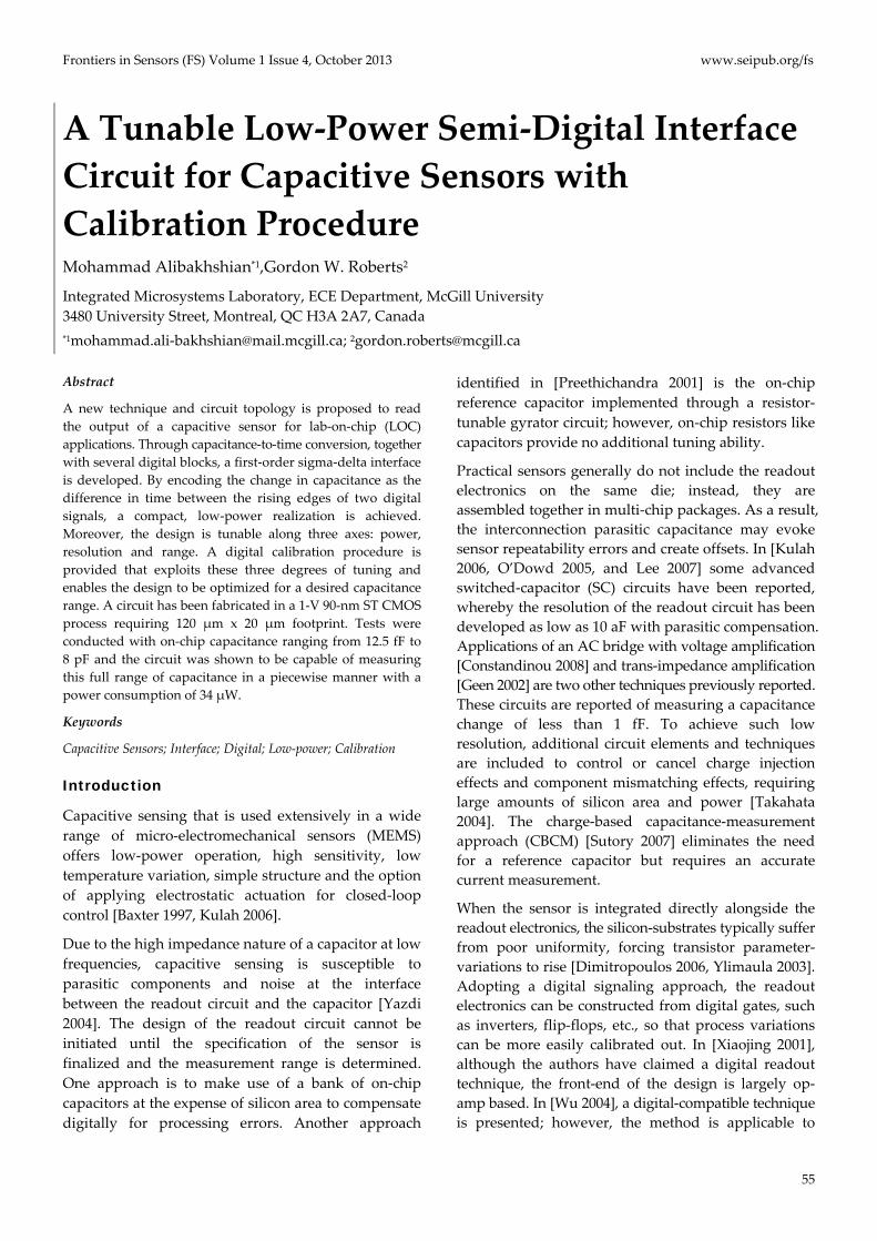
The voltage drop across the pre-charged capacitor in Fig. 1(a) being discharged by a constant current, IDischarge, is well defined using the equation
arg( )C DD
Disch e
CV t V tI
= − × (1)
By changing the capacitor, the slope of the discharge procedure changes linearly. By adding an inverter in cascade to the capacitor, the delay between the digital rising edges at ΦIN and ΦOUT can be calculated using
,
arg
( )DD Th invDelay
Disch e
C V VI
τ× −
= (2)
where VTh,inv is the threshold voltage of the inverter. For ease of reference, the delay is related to the capacitance variable using a proportionality coefficient, Gø, as
Delay G Cϕτ = (3)
Clearly, the delay of the circuit shown in Fig. 1(a) is linear in terms of the capacitor value and the block may be called a Capacitance-Controlled Delay Unit (CCDU). In Fig. 1(b), a CMOS circuit schematic to implement a CCDU is presented. The AND gate is used to ensure that the input falling edge at ΦIN is
propagated to the output without being influenced by the control capacitor; also, transistor M4 is included to discharge the control capacitor quickly and to bypass the delay of the block, where applicable. Fig. 2 shows the circuit symbol for the developed CCDU.
ΦIn
VDD
IDischarge
ΦIn
VC
(a) (b)
ΦOut
Vb
M1
M2
M3
M5
M6
ΦIn ΦOut
ΦInC
VBypassM4
FIG. 1 (a) THE LINEAR DISCHARGE OF A CAPACITOR, (b) CIRCUIT DIAGRAM FOR A CAPACITANCE-CONTROLLED
DELAY UNIT (CCDU)
CCDU
CCtrl
ΦOutΦIN
VBypassVb
FIG. 2 THE CIRCUIT SYMBOL FOR A CCDU
Adopting the linear capacitance-to-time conversion, a time-mode output will be produced that is the time difference between the digital rising edges at the input and output of the proposed CCDU. Due to the digital nature of the signals, digital circuits can be used alongside the CCDU to estimate the input capacitance. Using this technique, in the rest of this paper the detailed design of a first-order time-mode sigma-delta interface to readout the output of a capacitive sensor will be covered.
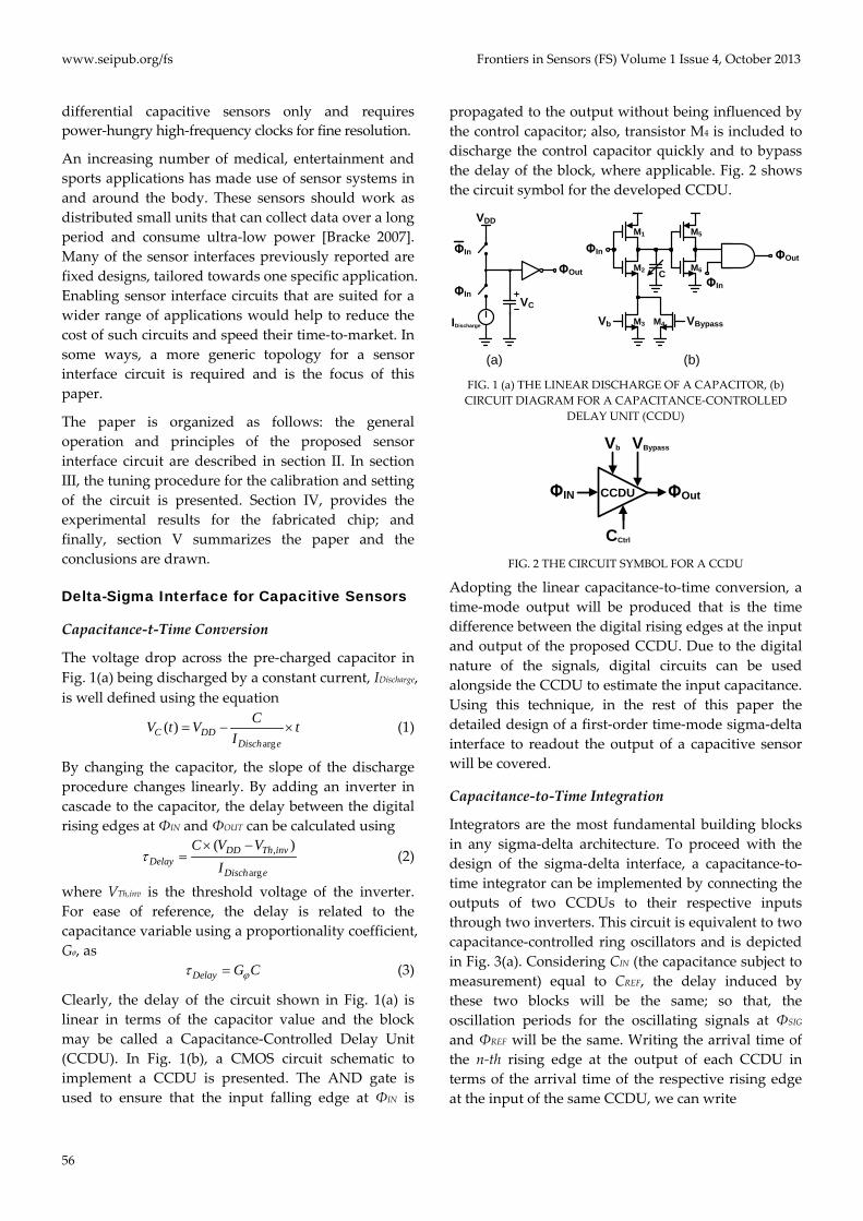
Capacitance-to-Time Integration
Integrators are the most fundamental building blocks in any sigma-delta architecture. To proceed with the design of the sigma-delta interface, a capacitance-to-time integrator can be implemented by connecting the outputs of two CCDUs to their respective inputs through two inverters. This circuit is equivalent to two capacitance-controlled ring oscillators and is depicted in Fig. 3(a). Considering CIN (the capacitance subject to measurement) equal to CREF, the delay induced by these two blocks will be the same; so that, the oscillation periods for the oscillating signals at ΦSIG and ΦREF will be the same. Writing the arrival time of the n-th rising edge at the output of each CCDU in terms of the arrival time of the respective rising edge at the input of the same CCDU, we can write
Frontiers in Sensors (FS) Volume 1 Issue 4, October 2013 www.seipub.org/fs
57
[ ] [ 1] [ 1]SIG I INt n t n G C nϕ= − + − (4) and
[ ] ' [ 1]REF I REFt n t n G Cϕ= − + (5) where, tI (t’I) and tSIG (tREF) represent the arrival time for the rising edges at the inputs and outputs of CCDU1 (CCDU2) respectively. Furthermore, the feedback path established by the inverter allows us to state
[ 1] [ 1] 2I SIG CCDU INVt n t n τ τ− = − + + (6) and
' [ 1] [ 1] 2I REF CCDU INVt n t n τ τ− = − + + (7) where, 2CCDU invτ τ+ is the total propagation delay of a low-to-high transition at the CCDU output back to its inputs as a low-to-high transition. Combining Eqns. (4)-(7), we can write
[ ] [ 1] [ 1] 2SIG SIG IN CCDU INVt n t n G C nϕ τ τ= − + − + + (8) and
[ ] [ 1] 2REF REF REF CCDU INVt n t n G Cϕ τ τ= − + + + . (9)
Finally, by subtracting Eqn. (9) from Eqn. (8), we obtain
[ ] [ ] [ ][ 1] [ 1]
OUT SIG REF
OUT IN
T n t n t nT n G C nϕ
∆ = −
= ∆ − + − (10)
CIN[n]
CREF
ΦO
ΦREF
n=0 n=1 n=2
ΔTO[1]=GΦCIN[0] ΔTO[2]=ΔTO[1]+GΦCIN[1]
ΔTO(0)
(a)
Time
CCDU1
CCDU2
Vb
(b) FIG. 3 (a) CAPACITANCE-TO-TIME INTEGRATOR. (b) TIMING
DIAGRAM FOR THE INTEGRATOR
Here, TOUT[n] represents the time difference between the rising edges at the outputs of the two oscillators. A timing diagram demonstrating three samples of the integrator operation is presented in Fig. 3(b). The initial integrator output time-difference, i.e. ΔTOUT[0], is assumed equal to zero. The next time-difference ΔTOUT[1] is shown proportional to the input capacitance at time instance n=0. The proceeding output ΔTOUT[2] is the sum of ΔTOUT[1] and the input capacitance CIN[1] scaled by Gø.
Sigma-Delta Interface
The developed capacitance-to-time integrator of Fig. 3(a) can be extended to a first-order sigma-delta modulator based on the error-feedback structure presented in Fig. 4 [Ali-Bakhshian 2009]. The output comparator by checking the sign of the output phase difference, i.e. ΔTOUT[n], represents a single-bit
quantizer. A D-type Flip/Flop (DFF) can be used as the output comparator. If the rising edge at the clock input leads the rising edge at the D input (for a negative phase difference), the output will be set to “0”; otherwise, for a positive phase difference it will be set to “1”. To implement the DAC feedback included in Fig. 4, the output bit should be applied directly to the bypass input of one of the CCDUs in the ring oscillators. This will cause the delay of the corresponding CCDU to be excluded from the loop delay when the DFF output DO is “1”, as well force the instantaneous period of the oscillation at the output of the corresponding oscillator to decrease. Otherwise, the propagation delay of this CCDU will be accumulated into the overall loop delay.
Z-1CIN[n]ΦREF
DO[n]ΦO
FIG. 4 BLOCK DIAGRAM FOR A FIRST-ORDER DELTA-SIGMA
MODULATOR
CCDU11 CCDU12 CCDU13
CCDU21 CCDU22 CCDU23
D
Q
Q
Vb Vb Vb
Vb Vb Vb
CREF
CbiasCbias
Cbias Cbias/2
CINCAP to be measured
DO
ΦO(n)
ΦREF(n)
FIG. 5 THE CIRCUIT SCHEMATIC FOR THE PROPOSED FIRST-ORDER DELTA-SIGMA SENSOR INTERFACE CIRCUIT
The complete diagram of the proposed sigma-delta-based interface is presented in Fig. 5 and it consists of two ring-oscillators and one DFF. For ease of reference, the top and the bottom oscillators will be referred to as the signal and the reference oscillators respectively. All CCDUs are biased at the fixed bias voltage of Vb. CCDU11 and CCDU21 operate as the input stage to convert the capacitance difference between CIN and CREF to a phase difference between the two oscillators. CCDU13 and CCDU23 with different control capacitors equal to Cbias and Cbias/2 are considered to implement the feedback. Finally, CCDU12 and CCDU22 with identical control capacitors equal to Cbias are included to set the duty cycle of the oscillating signal in each oscillator. Except for the bypass input to CCDU13 that is connected to the output of the DFF, all other CCDU bypass inputs are connected to ground.
As the discharge current, IDischarge, adopted in Eqn. (2) is
www.seipub.org/fs Frontiers in Sensors (FS) Volume 1 Issue 4, October 2013
58
controlled by Vb, this equation can be rewritten in general terms as a function of the bias voltage, i.e.
( )Delay bC f Vτ = × . (11)
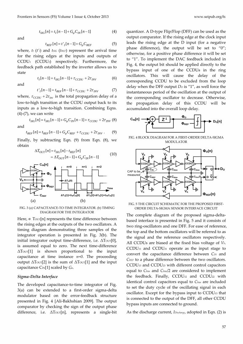
Now returning to the circuit of Fig. 5, the period of each oscillator can be derived by considering the propagation delay around each loop. In the case of a falling edge at the output of the reference oscillator, the propagation delay around the loop to invert it back to a rising edge equals
, 21 22
23
3 ( )
( )2
REF Low inv REF b CCDU
biasb
T C f VC
f V
τ τ= + × +
+ × (12)
where, we make use of the delay-Vb functional notation of Eqn. (11) for each CCDU in the loop. Likewise, the rising edge at the output of the reference oscillator comes back as a falling edge after
, 21 22 233 ( )REF High inv CCDU bias b CCDUT C f Vτ τ τ= + + × + .(13)
Apparently, the total period of any single oscillation at the output of the reference oscillator is
, ,REF REF Low REF HighT T T= + . (14)
Similar equations can be extracted for the signal oscillator as
, 11 12
13
3 ( )
(1 ) ( ).SIG Low inv IN b CCDU
O bias b
T C f VD C f V
τ τ= + × +
+ − × × (15)
and , 11 12 133 ( )SIG High inv CCDU bias b CCDUT C f Vτ τ τ= + + × + (16)
so that the total period for any single oscillation at the output of the signal oscillator is given by
, ,SIG SIG Low SIG HighT T T= + . (17)
Fig. 6 shows the timing signals for each oscillator output, ΦSIG and ΦREF. The reference oscillator provides the clock reference for the output comparator and its oscillation period is constant and independent of the input capacitance CIN and DFF state, DO. In contrast, the low-level width of the signal at ΦSIG is a function of both CIN and DO; thus making the period of this oscillator a function of the capacitance subject to measurement. As the DFF quantizes the accumulated time difference between the instantaneous periods of the two oscillator outputs, we can write
[ ][ ] [ 1]OUT OUT SIG REFT n T n T n T∆ = ∆ − + − (18)
)(2 2 bb ia sG a te s VfC ×+τ )(2
)( 2321 bbias
GatebREF VfCVfC ×++× τ
)(1 2 bb ia sG a tes VfC ×+τ )()1()( 1311 bbiasOG atebIN VfCDVfC ××−++× τΦO
ΦREF
FIG. 6 THE DURATION OF A SINGLE PERIOD OF THE SIG AND
REF OSCILLATORS
Substituting Eqns. (14) and (17), together with Eqns. (12), (13), (15) and (16) leads to a recursive expression for the instantaneous output time-difference TOUT[n]. In an ideal situation, CCDU11 identical to CCDU21, CCDU12 can be assumed identical to CCDU22, and CCDU13 identical to CCDU23. By considering the f(V) function representing each identical pair as f1(Vb), f2(Vb), and f3(Vb) respectively, the resulting expression becomes
1
3
[ ] [ 1] ( [ 1] ) ( )1( ) [ 1]2
OUT OUT IN REF b
bias b O
T n T n C n C f V
C f V D n
∆ = ∆ − + − − ×
+ × × − −
(19)
Assuming DO[n] is a digital signal toggling between “0” and “1”, the error signal ΔTε(n) induced by the DFF comparison may be expressed as the difference between the instantaneous output time difference and the size of the delay injected back into the loop, i.e.,
31[ ] [ ] ( ) [ ]2OUT bias b OT n T n C f V D nε
∆ = ∆ − × × −
(20)
Substituting Eqn. (20) into (19) reveals the first-order ΔΣ modulator difference equation as
{ }
{ }
1
3
3
( )[ ] [ 1]
( )1 1[ ] [ 1]
( ) 2
bO IN REF
bias b
bias b
f VD n C n C
C f V
T n T nC f V ε ε
= − −×
− ∆ −∆ − +×
. (21)
Fig. 7 presents an example illustrating the timing of four periods of the modulator’s operation with input condition, CIN = CREF. The period of oscillation for ΦREF is fixed; also, the high-level width of the oscillating signal at ΦSIG is fixed at TSIG,High. Here, it can be seen that how the low-level width of this signal toggles with constant input capacitance and DFF output.
ΔTO(1) ΔTO(2) ΔTO(3)
TO,High TO,High TO,High TO,HighTO,Low(-1) TO,Low(0) TO,Low(1) TO,Low(2)
n=0 n=1 n=2 n=3
ΦO
DO
TREF,Low TREF,Low TREF,Low TREF,LowTREF,High TREF,High TREF,High TREF,High
ΦREF
ΔTO(0)
FIG. 7 TIMING DIAGRAM OF A SHORT SEQUENCE OF THE
DELTA-SIGMA OPERATION
Linear Range of Operation
CREF is the reference value for the input capacitance CIN and the system is designed to measure any capacitance variation compared to CREF. By substituting CIN[n] = CREF+ΔC[n] into Eqn. (19), one can write an expression for the modulator output as:
1
3
[ ] [ 1] ( )1( ) [ 1]2
OUT OUT b
bias b O
T n T n C f V
C f V D n
∆ = ∆ − + ∆ ×
+ × × − −
(22)
Frontiers in Sensors (FS) Volume 1 Issue 4, October 2013 www.seipub.org/fs
59
For stable sigma-delta operation, the input amplitude of the modulator should be smaller than that of the feedback signal; so that the latter two terms associated with Eqn. (22) must undergo a full sign change. When the DFF output is in logic “0” state, we should have
31
( )( ) 0
2b
b biasf V
C f V C∆ × + × > (23)
Similarly, when DO=“1”, we should have 3
1( )
( ) 02
bb bias
f VC f V C∆ × − × < (24)
which leads to the following condition on the input capacitance for linear operation:
3 3
1 1
( ) ( )2 ( ) 2 ( )bias b bias b
b b
C f V C f VC
f V f V− × < ∆ < × . (25)
As TSIG,Low is a function of the input capacitance and state of the DFF, it can take on different values. If this time is longer than a period of the reference oscillator, as depicted in Fig. 8, it is possible to lose one full cycle of the reference oscillator, e.g., create a cycle slip. To avoid such a condition, the timing for both oscillator outputs should satisfy the following relation,
, ,02
OHigh SIG Low High REF LowD
T T T T=
+ ≤ + (26)
where we assume THigh= TREF,High= TSIG,High. Substituting corresponding expressions for each variable in Eqn. (26) results in a further simplified expression as
1 3( ) ( )2bias
High b bC
T C f V f V≥ ∆ × + × . (27)
ΦREF[n]
ΦO[n]
DO[n]
TREF,LowTREF,High TREF,LowTREF,High
TO,High TO,HighTO,Low, DO=0
FIG. 8 THE FEEDBACK PUSHING THE CIRCUIT OUT OF LINEAR
OPERATION
The inequality shown in Eqn. (27) should be satisfied even for the largest value of the input capacitance specified by (25); ignoring the minor values for gate delays, and Eqn. (27) can be reduced to
2 3( ) ( )b bf V f V≥ (28)
This expression indicates that for the same control capacitor, Cbias, the delay induced by CCDU12 and CCDU22 should be equal or greater than the delay induced by CCDU13 and CCDU23.
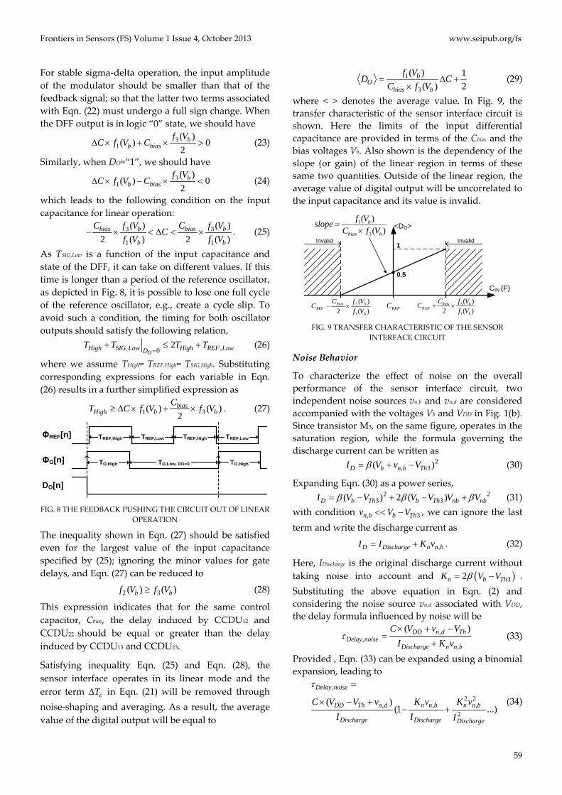
Satisfying inequality Eqn. (25) and Eqn. (28), the sensor interface operates in its linear mode and the error term Tε∆ in Eqn. (21) will be removed through noise-shaping and averaging. As a result, the average value of the digital output will be equal to
1
3
( ) 1( ) 2
bO
bias b
f VD C
C f V= ∆ +
× (29)
where < > denotes the average value. In Fig. 9, the transfer characteristic of the sensor interface circuit is shown. Here the limits of the input differential capacitance are provided in terms of the Cbias and the bias voltages Vb. Also shown is the dependency of the slope (or gain) of the linear region in terms of these same two quantities. Outside of the linear region, the average value of digital output will be uncorrelated to the input capacitance and its value is invalid.
)()(
2 1
3
b
bbiasEFR Vf
VfCC ×+REFC
)()(
3
1
bbias
b
VfCVfslope×
=
InvalidInvalid
<DO>
CIN (F)
0.5
1
)()(
2 1
3
b
bbiasREF Vf
VfCC ×−
FIG. 9 TRANSFER CHARACTERISTIC OF THE SENSOR
INTERFACE CIRCUIT
Noise Behavior
To characterize the effect of noise on the overall performance of the sensor interface circuit, two independent noise sources vn,b and vn,d are considered accompanied with the voltages Vb and VDD in Fig. 1(b). Since transistor M3, on the same figure, operates in the saturation region, while the formula governing the discharge current can be written as
2, 3( )D b n b ThI V v Vβ= + − (30)
Expanding Eqn. (30) as a power series, 2 2
3 3( ) 2 ( )D b Th b Th nb nbI V V V V V Vβ β β= − + − + (31) with condition , 3n b b Thv V V<< − , we can ignore the last term and write the discharge current as
,D Discharge n n bI I K v= + . (32)
Here, IDischarge is the original discharge current without taking noise into account and ( )32n b ThK V Vβ= − . Substituting the above equation in Eqn. (2) and considering the noise source vn,d associated with VDD, the delay formula influenced by noise will be
,,
,
( )DD n d ThDelay noise
Discharge n n b
C V v VI K v
τ× + −
=+
(33)
Provided , Eqn. (33) can be expanded using a binomial expansion, leading to
,
2 2, , ,
2
( )(1 ...)
Delay noise
DD Th n d n n b n n b
Discharge Discharge Discharge
C V V v K v K vI I I
τ =
× − +− +
(34)
www.seipub.org/fs Frontiers in Sensors (FS) Volume 1 Issue 4, October 2013
60
Considering Eqn. (2) and ignoring the second and higher order components in (34), the formula for delay of a CCDU block can be written as the sum of a noise-free term and a noise component, i.e.
,Delay noise Delay Noiseτ τ τ= + (35)
where Noiseτ is given by
, , , ,2Delay n n
Noise n d n b n b n dDischarge Discharge Discharge
K K CC v v v vI I I
ττ = − + (36)
Assuming that vn,b and vn,d are two noise sources uncorrelated with zero mean value, the expected value of the jitter will be equal to zero and the mean square value of the jitter will be
, ,
2 222 2 2
2 2n d n b
Delay nv v
Discharge Discharge
KCI Iτ
τσ σ σ= + (37)
The delay around each loop is the summation of the delays of the CCDUs in that loop. So, each oscillating signal undergoes the same type of jitter as a single CCDU block, albeit with some scaling coefficient between 1 and 3. Hence, Eqn. (37) provides the key noise behavior of each oscillator.
Impact of Temperature
Due to temperature gradient over the wafer, the threshold voltage of the transistors and the mobility of the charge carriers are subject to change. As shown in the section for the experimental results, the footprint of the implemented design is very small. This guarantees that by adopting some basic matching techniques such as common-centroid or interdigitized structures, corresponding CCDUs in both oscillators undergo the same temperature variation; so that the temperature-dependant mismatches between the oscillators will be negligible. Also, as temperature changes ( )1 bf V in Eqn. (29) change in the same direction as ( )3 bf V ; consequently, the temperature sensitivity of the output, i.e. OD that is equal to the ratio of these two values can be designed to be quite small.
Impact of Transistor Mismatches
The architecture of the proposed circuit is differential and the reference and signal oscillators are supposed to be identical but have different control capacitors. However, mismatches are unavoidable in any CMOS process and it is impossible to have the two ring-oscillators completely matched. As shown in Fig. 5, each component contributes to the overall performance of the modulator by the propagation delay of the signal passing through that component.
Mismatches between the threshold voltages, discharge currents, dimensions, and etc of the corresponding elements in two oscillators will show up as the difference between their loop delays. By considering a different f(Vb) for each individual CCDU to model the mismatch effect and by reviewing the steps taken to extract Eqn. (29), this equation changes as
[ ] ( )( ) [ ]( )1
3
112
MMatch bO IN REF
bias b
K f VD n C n C
C f V×
′= − − +×
. (38)
Apparently, mismatches change the slope of the transfer characteristic by a factor of MMatchK ; also, the effective value for the REFC changes to REFC′ . These changes, however, are independent of the input capacitor and they do not result in any non-linearity. As explained in the next section, the effect of mismatches can be easily calibrated through a tuning procedure on start-up.
Tuning and Controlling the Sensor Interface Circuit
Changing CREF and the range/sensitivity of the circuit
As previously explained, each pair of CCDUs adopted in the sensor interface circuit was presented by a different function as f1(Vb), f2(Vb), or f3(Vb). By controlling each individual CCDU, more control over the range of operation and sensitivity of the circuit will be possible. For the rest of this paper, CCDU11 and CCDU21 will be represented by different functions f11(Vb) and f21(Vb), respectively, and Eqns. (25) and (29) will change accordingly as
3 3
11 11
( ) ( )2 ( ) 2 ( )bias b bias b
b b
C f V C f VC
f V f V− × < ∆ < × . (39)
and 11
3
( ) 1( )( ) 2
bO IN REF
bias b
f VD C C
C f V= − +
× (40)
As explained in the previous sections, each control capacitor contributes to the circuit by influencing the partial delays around each loop, as formulated by Eqn. (11). By changing CREF in the modulator shown in Fig. 5 to REFn C× , the delay induced by CCDU21 will be equal to
21 21( )Delay REF bn C f Vτ = × × , (41)
which can be rewritten as 21 21( ' )Delay REF bC f Vτ = × , (42)
Eqns. (41) and (42) indicate that there are two ways in which the same delay can be achieved. One is to use a capacitance of REFn C× and the other way is to use a different bias voltage of bV ′ . By increasing bV , the

Frontiers in Sensors (FS) Volume 1 Issue 4, October 2013 www.seipub.org/fs
61
magnitude of f(Vb) decreases; consequently, for a fixed value of REFC the delay induced by this capacitor decreases. So, the bias voltage applied to CCDU21 can be used to change the effect of the reference capacitance of the sensor interface circuit while the range of operation and the sensitivity of the sensor interface circuit do not change. To proceed with this idea, the new concept of equivalent capacitance reference level, CREF,EQV, can be defined as
( ), 21 'REF EQV REF bC C n V= × , (43)
and ( )21 'bn V represents the scaling factor controlled by the bias voltage connected to CCDU21.
The same process might be implemented to modify the sensitivity of the sensor interface circuit. With respect to Eqn. (40), for the same output range, scaling the numerator term f11(Vb) by some factor, say α , the input differential capacitance CIN-CREF,EQV can be scaled by the factor 1/α . This situation is depicted in Fig. 10 for two different bias conditions 1bV and 2bV when
1 2b bV V< . Here we make use of the functional representation
( ) ( )( )
3
11 22bbias
bb
f VCV
f Vλ = (44)
,n n b DischargeK v I<
)()()(
3
1111
bbias
bb VfC
VfVslope×
=
<DO>
CIN (F)
1
0.5
)()()(
3
2112
bbias
bb VfC
VfVslope×
=
CREF×n21(Vb)+λ(Vb2)
CREF×n21(Vb)+λ(Vb1)
CREF×n21(Vb)-λ(Vb1)
CREF×n21(Vb)-λ(Vb2)
CREF×n21(Vb)
FIG. 10 TRANSFER CHARACTERISTIC OF THE SENSOR
INTERFACE CIRCUIT FOR TWO DIFFERENT BIAS CONDITIONS ON CCDU11
In effect, changing the bias voltage of CCDU21 changes the equivalent reference capacitance and changing the bias of CCDU11 changes the sensitivity of the circuit. Collectively, these two control variables enable the circuit to operate over a wide range of input capacitance conditions.
The reader may be worried about the number of design specs and control variables to be set; however, all this information is included to demonstrate the flexibility of the proposed design. In an application–oriented design and based on the degrees of freedom required, the transfer characteristic of the interface circuit can be simplified by ignoring some of the above tunablity features.
The Detection of Non-linear Operation
If the sensor interface behaves linearly, for each cycle of the signal oscillator there should be a corresponding cycle from the reference oscillator. If one of the rising edges is missing, it is good evidence that the input capacitance is out of linear range, as explained shortly. By observing the output of each oscillator, together with the state of the D-type F/F, a digital code can be devised that keeps track of the sequence of events occurring within the circuit. One component of the digital code consists of the order in which the rising edges appear at the output of each oscillator. For example, if the rising edge for the reference oscillator appears after the one for the signal oscillator and we denote the reference rising edge with symbol “” and the oscillator rising edge with symbol “A”, then one part of the output code would be written as “A”. If this sequence continues then the output code would appear as “AAA…”. The other component of this code consists of the state of the output D-type F/F at the rising edge of the signal oscillator. We combine these two code components by substituting symbol “A” by the corresponding state of the F/F. For instance, if the state of the F/F follows the sequence “110”, then the combined code would be “110…”.
When CIN is less than the minimum value allowed, the period of the signal oscillator will be shorter than the period of the reference oscillator and even the feedback signal cannot change this condition. Similarly, if CIN is greater than its maximum allowed value, the signal oscillator period will be longer than the period of the reference oscillator and the feedback signal cannot correct this situation either. These two situations result in a set of error codes that indicate nonlinear operation.
In Fig. 11(a) three situations are shown where the signal oscillator period is less than the reference oscillator period. Considering the first situation involving ΦREF and ΦO1, the maximum period of ΦO1 is slightly shorter than the period of ΦREF; after a few cycles, two rising edges for ΦO1 happens within one cycle of ΦREF. This situation results in the code sequence of “01” representing the missing rising edge for ΦREF. The correct sequence should have been “01”. Another situation depicted by ΦO2 and ΦO3 captures the situation where the period of signal oscillator is much shorter and two successive rising edges of the signal oscillator may sample one identical digital level of ΦREF. As a result, the sequence of “11” or “00” will be produced within the output. The appearance of each one of these three error codes
www.seipub.org/fs Frontiers in Sensors (FS) Volume 1 Issue 4, October 2013
62
confirms that the input CIN is less than the allowed minimum value. Similarly, Fig. 11(b) shows four situations when CIN exceeds its maximum allowable value. Considering the first situation involving reference signal ΦREF and signal oscillator ΦO1, even after applying the feedback DO=“1”, the period of signal oscillator is slightly greater than the period for reference oscillator. After a few cycles, one complete cycle of the reference oscillator will be missed and an error sequence of “10” appears where the correct sequence is “10”. Other situations depicted in Fig. 11(b) corresponding to CIN being much greater than the upper bond and resulting in higher number of missed cycles are captured by signals ΦO2, ΦO3, and ΦO4. In much the same way as described for the previous code, error codes “1”, “00”, and “0” can be used to identify the nonlinear situations corresponding to them. It can be concluded that the input capacitance, CIN, is out of range as soon as any one of these codes is detected.
0 1
0 0
1 1
00
1
0
x0 1xx00xx11x
Error Codes
1 0
1 X
0
0 X
0
Error Codes
x1 0xx1 xx0 0xx0 x
(a)
(b)
ΦO1
ΦREF
ΦO2
ΦO3
ΦO4
ΦO1
ΦREF
ΦO2
ΦO3
FIG. 11 (a) ERROR CODES TO DETECT A CIN <CIN,Min SITUATION,
(b) ERROR CODES TO DETECT A CIN >CIN,Max SITUATION
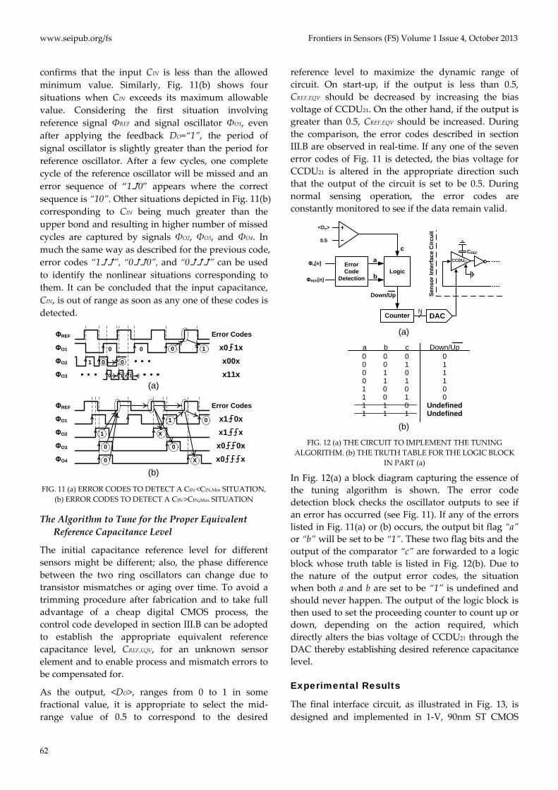
The Algorithm to Tune for the Proper Equivalent Reference Capacitance Level
The initial capacitance reference level for different sensors might be different; also, the phase difference between the two ring oscillators can change due to transistor mismatches or aging over time. To avoid a trimming procedure after fabrication and to take full advantage of a cheap digital CMOS process, the control code developed in section III.B can be adopted to establish the appropriate equivalent reference capacitance level, CREF,EQV, for an unknown sensor element and to enable process and mismatch errors to be compensated for.
As the output, <DO>, ranges from 0 to 1 in some fractional value, it is appropriate to select the mid-range value of 0.5 to correspond to the desired
reference level to maximize the dynamic range of circuit. On start-up, if the output is less than 0.5, CREF,EQV should be decreased by increasing the bias voltage of CCDU21. On the other hand, if the output is greater than 0.5, CREF,EQV should be increased. During the comparison, the error codes described in section III.B are observed in real-time. If any one of the seven error codes of Fig. 11 is detected, the bias voltage for CCDU21 is altered in the appropriate direction such that the output of the circuit is set to be 0.5. During normal sensing operation, the error codes are constantly monitored to see if the data remain valid.
Counter
LogicError Code
Detection
CCDU21
CREF
DACN
Φo[n]
ΦREF[n]
<Do>
0.5c
b
a
Down/Up Sens
or In
terf
ace
Circ
uit
Down/Upa b c00
0001111
00110011
01010101
11100
UndefinedUndefined
(a)
(b) FIG. 12 (a) THE CIRCUIT TO IMPLEMENT THE TUNING
ALGORITHM. (b) THE TRUTH TABLE FOR THE LOGIC BLOCK IN PART (a)
In Fig. 12(a) a block diagram capturing the essence of the tuning algorithm is shown. The error code detection block checks the oscillator outputs to see if an error has occurred (see Fig. 11). If any of the errors listed in Fig. 11(a) or (b) occurs, the output bit flag “a” or “b” will be set to be “1”. These two flag bits and the output of the comparator “c” are forwarded to a logic block whose truth table is listed in Fig. 12(b). Due to the nature of the output error codes, the situation when both a and b are set to be “1” is undefined and should never happen. The output of the logic block is then used to set the proceeding counter to count up or down, depending on the action required, which directly alters the bias voltage of CCDU21 through the DAC thereby establishing desired reference capacitance level.
Experimental Results
The final interface circuit, as illustrated in Fig. 13, is designed and implemented in 1-V, 90nm ST CMOS

Frontiers in Sensors (FS) Volume 1 Issue 4, October 2013 www.seipub.org/fs
63
technology. To satisfy Eqn. (28), identical bias voltages are used to bias CCDU12, CCDU22, CCDU13, and CCDU23. Voltage Vb-Sen is used to control CCDU11 in order to adjust the sensitivity of the circuit. CCDU21 is controlled by Vb-Ref, the voltage responsible to establish the equivalent reference capacitance as explained earlier. To implement the control routines, ΦO and ΦREF are taken off of the chip through buffers. As explained earlier, these outputs will be used to detect error codes declaring the non-linear performance of the circuit.
CCDU21
D
Q
Q
Vb-Sen
CREF
CbiasCbias
Cbias Cbias/2
DO
ΦO
ΦREFVb-Ref
CIN
VDD
Gnd
Vb
CCDU11 CCDU12 CCDU13
CCDU23CCDU22
FIG. 13 THE COMPLETE DIAGRAM OF THE TIME-MODE
DELTA-SIGMA INTERFACE
Capacitor Bank
Delta-Sigma Interface
FIG. 14 THE MICROPHOTOGRAPH OF THE IMPLEMENTED
DELTA-SIGMA INTERFACE
CREF and Cbias capacitors have been implemented using 0.5 pF fringe-capacitors alongside a bank of capacitors on-chip consisting of 12.5 fF, 25 fF, 50 fF, 100 fF, 200 fF, 400 fF, 800 fF, 1 pF, 2 pF, 4 pF, and 7 pF fringe-capacitors. Depending on the test, a combination of these capacitors will be applied to the input pin CIN. Generally, the test conditions consists of one input bias capacitor of values 0 pF, 1 pF, 2 pF, 4 pF or 7 pF together with some combination of the remaining capacitors called the signal capacitors. The signal capacitor components alter the input capacitance with respect to the input bias capacitance level (i.e. the signal with respect to a bias level). The sensor interface circuit should adapt CREF,EQV such that it equals the input bias capacitance level. A microphotograph of the die is shown in Fig. 14 and it occupies an area of 120
μm x 20 μm including the output buffers.
FIG. 15 THE CAPACITOR PROFILE OF THE IMPLEMENTED
CAPACITOR BANK
FIG. 16 THE JITTER NOISE ASSOCIATED WITH THE CIRCUIT
Each capacitor in the capacitor bank is individually characterized with respect to the open circuit situation whereby no capacitance is connected to the input pin CIN. This was conducted by measuring the period of the signal oscillator. According to Eqns. (12)-(17), the expected change in the oscillation period is a linear function of the input capacitance CIN. Using a Le Croy digital scope (model SDA-6000), the oscillation period for 10,000 cycles of ΦO was measured and averaged to extract the actual capacitance value realized on-chip. For different bias voltages Vb-Sen ranging from 0.3 to 0.7 V, the change in the oscillator period versus the input signal capacitance was determined and is shown in Fig. 15(a). Lines have been drawn between each data point for ease of illustration. Also, the x-axis represents the nominal capacitor values or bins drawn on a nonlinear axis for ease of reference. By dividing and normalizing each curve in Fig. 15(a) to its highest value, the plot in Fig. 15(b) was derived. As evident, all curves were normalized to essentially the same graph, indicating the linearity of the method used to characterize the various input capacitor values. This graph will be considered as the capacitor profile to be measured. Also in Fig. 16 and extracted out of 10,000 samples, the distribution percentage for the jitter associated with

www.seipub.org/fs Frontiers in Sensors (FS) Volume 1 Issue 4, October 2013
64
each oscillating signal relative to the period of oscillation is shown. The distribution pattern is very much Gaussian with a zero mean and a standard deviation of 0.076% of the oscillation period.
To measure the integrated capacitor bank, this time the proposed sensor interface circuit was used. The test setup is shown in Fig. 17. The voltage at pin Vb is connected to a middle level voltage and the voltage at pins Vb-Sen and Vb-Ref are set using two different DACs. For any input capacitance, the output ΦO and ΦREF are forwarded to the control unit to make sure that the interface works in its linear mode. After assigning a voltage to Vb-Sen through DAC1 and using the tuning algorithm described earlier, the control unit modifies the input to DAC2 to set the proper CREF,EQV such that it equals the input bias capacitance level. During this process, any mismatche between the two oscillators will be corrected, as well. The sensitivity of the sensor interface circuit is modified using DAC1 such that the gain is maximized over some desired capacitance range. In our specific case, an external known signal capacitor is connected in parallel with some input bias capacitance and the sensor interface circuit output is monitored such that the slope of the output versus input signal capacitance reaches a desired level. Any modification in the sensitivity of the circuit should be followed by a tuning algorithm.
Accumulator
Vb-Sen
DO
ΦO
ΦREF
Vb-RefCIN
VDD
GndVb
DAC2
DAC1
Control Unit
8 bi
t
8 bi
t
NOUTVCC
C1C2C3CN-1CN
RPOT
On-chip fringe capacitor bank
FIG. 17 THE DIAGRAM SCHEME FOR THE TEST CIRCUIT
The data captured by the sensor interface circuit is shown in Fig. 18(a) in normalized format. The input bias capacitance was varied within 0 pF, 1 pF, 2 pF, 4 pF and 7 pF while the input signal capacitance was varied from 0 pf to 800 fF. As evident, the data is very similar for each bias condition, again indicating very good linearity. The relative absolute error in percent was computed with respect to the curve derived earlier through the oscilloscope measurements associated with the oscillation period (Fig. 15(b)) and the results are shown in Fig. 18(b). Here the data is identified according to the input bias capacitance level. For small values of input signal capacitance, the relative error is greatest. It is also evident that the
relative error is the largest when the input bias capacitance is at its maximum input value of 7 pF. These results appear to be consistent over several separate sets of measurements. This indicates that noise strongly affects the lower range of the measurements. This is not too surprising, as the variance of the jitter associated with each oscillator output is directly proportional to the input bias capacitance level as seen in Eqn. (37). This implies that the accuracy of the sensor interface is better at smaller input bias capacitance levels than that at larger ones.
FIG. 18 (a) THE CHARACTERIZED INPUT CIN BETWEEN ZERO
AND 800 FF WITH DIFFERENT INPUT BIAS CAPACITANCE, (b) ABSOLUTE ERROR ASSOCIATED WITH MEASUREMENTS IN
PART (a)
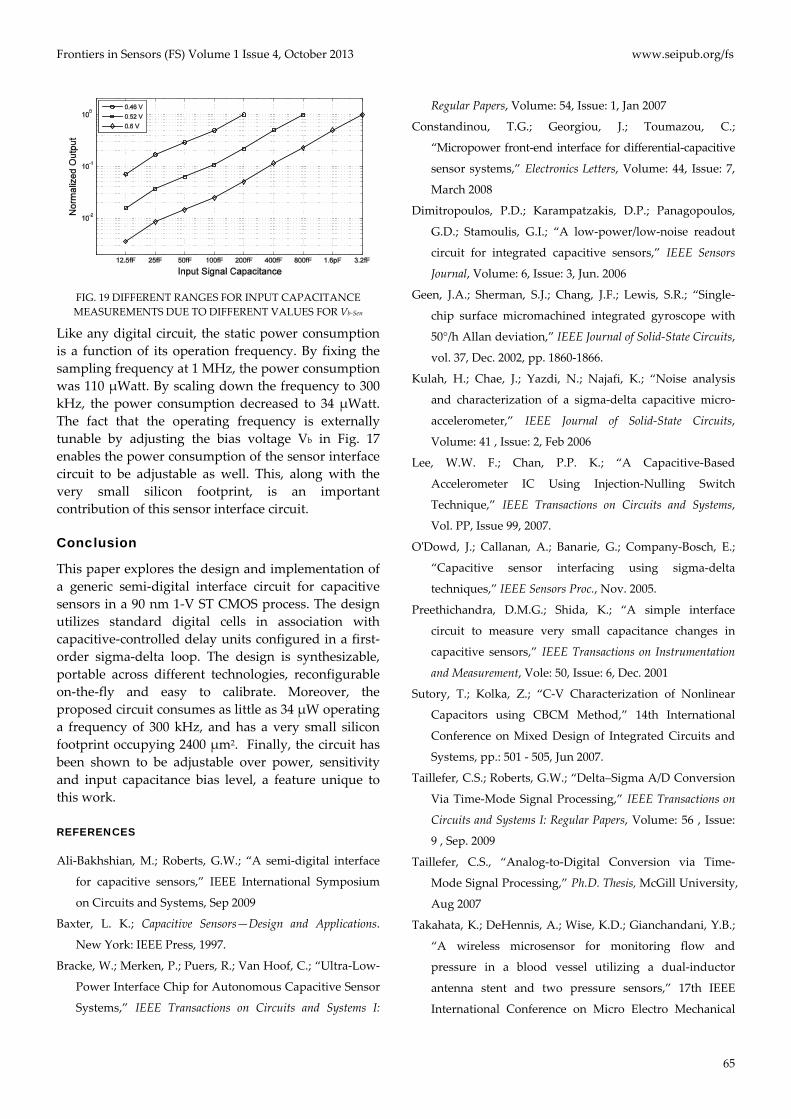
To illustrate the ability of the circuit to adjust its input range, the input to DAC2 was changed to modify the sensitivity of the sensor interface circuit. Three specific examples are shown in Fig. 19 for Vb-Sen equal to 0.32 V, 0.44 V and 0.51V. In all cases, the input bias capacitance was fixed to be 0 fF and the input signal capacitance was incrementally increased to a maximum value of 2 pF. Here it is evident how the upper bound on the input signal capacitance range was adjusted from 200 fF to 2 pF. When these three curves are compared, the capacitor profile extracted in Fig. 15(b), some error is evident. Specifically, at very small signal capacitance levels of 12.5 fF, the relative error varies from 2% to 67% as the sensitivity of the sensor interface circuit decreases (i.e., signal range increases).
Frontiers in Sensors (FS) Volume 1 Issue 4, October 2013 www.seipub.org/fs
65
FIG. 19 DIFFERENT RANGES FOR INPUT CAPACITANCE MEASUREMENTS DUE TO DIFFERENT VALUES FOR Vb-Sen
Like any digital circuit, the static power consumption is a function of its operation frequency. By fixing the sampling frequency at 1 MHz, the power consumption was 110 μWatt. By scaling down the frequency to 300 kHz, the power consumption decreased to 34 μWatt. The fact that the operating frequency is externally tunable by adjusting the bias voltage Vb in Fig. 17 enables the power consumption of the sensor interface circuit to be adjustable as well. This, along with the very small silicon footprint, is an important contribution of this sensor interface circuit.
Conclusion
This paper explores the design and implementation of a generic semi-digital interface circuit for capacitive sensors in a 90 nm 1-V ST CMOS process. The design utilizes standard digital cells in association with capacitive-controlled delay units configured in a first-order sigma-delta loop. The design is synthesizable, portable across different technologies, reconfigurable on-the-fly and easy to calibrate. Moreover, the proposed circuit consumes as little as 34 μW operating a frequency of 300 kHz, and has a very small silicon footprint occupying 2400 μm2. Finally, the circuit has been shown to be adjustable over power, sensitivity and input capacitance bias level, a feature unique to this work.
REFERENCES
Ali-Bakhshian, M.; Roberts, G.W.; “A semi-digital interface
for capacitive sensors,” IEEE International Symposium
on Circuits and Systems, Sep 2009
Baxter, L. K.; Capacitive Sensors—Design and Applications.
New York: IEEE Press, 1997.
Bracke, W.; Merken, P.; Puers, R.; Van Hoof, C.; “Ultra-Low-
Power Interface Chip for Autonomous Capacitive Sensor
Systems,” IEEE Transactions on Circuits and Systems I:
Regular Papers, Volume: 54, Issue: 1, Jan 2007
Constandinou, T.G.; Georgiou, J.; Toumazou, C.;
“Micropower front-end interface for differential-capacitive
sensor systems,” Electronics Letters, Volume: 44, Issue: 7,
March 2008
Dimitropoulos, P.D.; Karampatzakis, D.P.; Panagopoulos,
G.D.; Stamoulis, G.I.; “A low-power/low-noise readout
circuit for integrated capacitive sensors,” IEEE Sensors
Journal, Volume: 6, Issue: 3, Jun. 2006
Geen, J.A.; Sherman, S.J.; Chang, J.F.; Lewis, S.R.; “Single-
chip surface micromachined integrated gyroscope with
50°/h Allan deviation,” IEEE Journal of Solid-State Circuits,
vol. 37, Dec. 2002, pp. 1860-1866.
Kulah, H.; Chae, J.; Yazdi, N.; Najafi, K.; “Noise analysis
and characterization of a sigma-delta capacitive micro-
accelerometer,” IEEE Journal of Solid-State Circuits,
Volume: 41 , Issue: 2, Feb 2006
Lee, W.W. F.; Chan, P.P. K.; “A Capacitive-Based
Accelerometer IC Using Injection-Nulling Switch
Technique,” IEEE Transactions on Circuits and Systems,
Vol. PP, Issue 99, 2007.
O'Dowd, J.; Callanan, A.; Banarie, G.; Company-Bosch, E.;
“Capacitive sensor interfacing using sigma-delta
techniques,” IEEE Sensors Proc., Nov. 2005.
Preethichandra, D.M.G.; Shida, K.; “A simple interface
circuit to measure very small capacitance changes in
capacitive sensors,” IEEE Transactions on Instrumentation
and Measurement, Vole: 50, Issue: 6, Dec. 2001
Sutory, T.; Kolka, Z.; “C-V Characterization of Nonlinear
Capacitors using CBCM Method,” 14th International
Conference on Mixed Design of Integrated Circuits and
Systems, pp.: 501 - 505, Jun 2007.
Taillefer, C.S.; Roberts, G.W.; “Delta–Sigma A/D Conversion
Via Time-Mode Signal Processing,” IEEE Transactions on
Circuits and Systems I: Regular Papers, Volume: 56 , Issue:
9 , Sep. 2009
Taillefer, C.S., “Analog-to-Digital Conversion via Time-
Mode Signal Processing,” Ph.D. Thesis, McGill University,
Aug 2007
Takahata, K.; DeHennis, A.; Wise, K.D.; Gianchandani, Y.B.;
“A wireless microsensor for monitoring flow and
pressure in a blood vessel utilizing a dual-inductor
antenna stent and two pressure sensors,” 17th IEEE
International Conference on Micro Electro Mechanical

www.seipub.org/fs Frontiers in Sensors (FS) Volume 1 Issue 4, October 2013
66
Systems (MEMS), 2004
Wu, J.; Fedder, G.K.; Carley, L.R.; “A low-noise low-offset
capacitive sensing amplifier for a 50-μg/√Hz monolithic
CMOS MEMS accelerometer”, IEE Journal of Solid-State
Circuits, vol. 39, pp. 722-730, May 2004.
Xiaojing Shi; Matsumoto, H.; Murao, K.; “A high-accuracy
digital readout technique for humidity sensor,” IEEE
Transactions on Instrumentation and Measuremen, Volume:
50, Issue: 5 , Oct. 2001
Yazdi, N.; Kulah, H.; Najafi, K.; “Precision readout circuits
for capacitive micro-accelerometers,” IEEE Sensors Proc.,
Oct. 2004.
Ylimaula, M.; Aberg, M.; Kiihamaki, J.; Ronkainen, H.;,
“Monolithic SOI-MEMS capacitive pressure sensor with
standard bulk CMOS readout circuit,” Proceedings of the
29th European Solid-State Circuits Conference (ESSCIRC),
2003
Mohammad Alibakhshian was born in Tehran, Iran, in 1978. He received the B.Sc. degree from Tehran Polytechnic in 2001, the M.Sc. degree from Sharif University of Technology in 2003, and the Ph.D degree from McGill University in 2012. His Ph.D. research focused on Time-to-Digital converters (TDCs) and the
development of time-mode signal processing techniques for the digital implementation of analog functions.
In 2012, Dr. Alibakhshian joined Synopsys mixed-signal design group in Toronto as a senior analog designer.
Gordon W. Roberts received the B.A.Sc. degree from the University of Waterloo, Canada, in 1983 and the M.A.Sc. and Ph.D. degrees from the University of Toronto, Canada, in 1986 and 1989, respectively, all in electrical engineering. At McGill University he is a full professor and holds the James McGill
Chair in Electrical and Computer Engineering. He has co-written six textbooks related to analog IC design and mixed-signal test. He has published numerous papers in scientific journals and conferences, and he has contributed chapters to various industrially focused textbooks. Dr. Roberts has held many administration roles within various conference organizations, such as the International Test Conference, Custom Integrated Circuit Conference, Design Automation Conference and the International Symposium on Circuits and Systems. He was the 2009 General Chair of the International Test Conference. Dr. Roberts is named on 10 patents, and has received numerous department, faculty and university awards for teaching test and electronics to undergraduates, and received several IEEE awards for his work on mixed-signal testing. Most notably, he has been awarded the 1992, 1993 and 2000 best or honorable mention papers at the International Test Conference. Several of his papers are published in the 2004 most significant papers published in the past 35 years of ITC.
Dr. Roberts has supervised over 50 graduate students at the Masters and PhD level. In 2003 he took leave from McGill to co-found DFT Microsystems, Inc, a company specializing in high-speed timing measurement. He returned to McGill 2005 where his current research includes analog IC design methods and built-in self-test techniques for analog and high-speed digital circuits. Dr. Roberts is a Fellow of the IEEE.