Embed Size (px)
Citation preview

Low-Cost High-Efficiency Solar Cells with Wafer Bonding and Plasmonic Technologies
Thesis by Katsuaki Tanabe
In Partial Fulfillment of the Requirements for the Degree of
Doctor of Philosophy
California Institute of Technology Pasadena, California
2008
(Defended May 21, 2008)

ii
© 2008
Katsuaki Tanabe
All Rights Reserved

iii
Acknowledgements
First of all, I would like to thank my thesis adviser Harry Atwater for his great
mentorship and guidance over the years. While he is an extremely busy professor holding
about twenty students in his research group and a lot of domestic and international travels
for seminars and conferences, he never hesitated to discuss with me when I knocked on
his office’s door. Our discussion often went over 1 hour in his tight schedule, but he did
not stop until we reached clear conclusions and decided what to do next. While he always
tries to find the most effective way for experimental scheme, Harry one day told me that
we engineers should always assume possible to fabricate whatever structure possible
when I showed a hesitation for doing a complicated process, which preach is still and will
be in my mind.
It was also a great pleasure for me to work with the excellent members in the Atwater
research group. Anna Fontcuberta i Morral, a fromer postdoc through 2002 to 2003 and
currently a research group leader in Walter Schottky Institute in Germany, was a mentor
when I first came to Caltech in summer 2003. She gave me an exclusive guidance for
wafer bonding and layer transfer technique. Jimmy Zahler, a former grad student
graduating in 2005 and currently at BP Solar, also gave me a lot of advice for wafer
bonding and multijunction solar cell structures. He was also one of my collaborators as
the technical leader at Aonex Technologies for the project in Chapters 5 and 6. Melissa
Archer, the other student member of the III-V solar cell subgroup, has been giving me
various technical supports particularly for our home-made solar simulator setup and
useful discussions on the multijunction solar cell projects as well as sharing the pain to
iv
wait long for the growth by the busy scientists at Spectrolab. She also helped me a lot for
the semiconductor polishing process, giving me a ride to UCLA Nanolab. Keisuke
Nakayama, a visiting scholar from Nippon Oil in Japan, joined the group late 2006 and
accelerated the plasmonic solar cell research progress in Chapter 7 with his more-than-
precise nanoparticle making technique. For Chapter 7, I also received a lot of advices on
plasmonics from Rene de Waele, Jen Dionne, Vivian Ferry, Henri Lezec, Domenico
Pacifici and Luke Sweatlock. Without those people, I would not have realized the
significance and excitement of plasmonic technologies. I had nice discussions on solar
cell basic principles and potential future technologies with Brendan Kayes and Christine
Richardson from the silicon solar cell team. They helped me also for the sample
preparation for SIMS measurements, solar simulator setup, e-beam lithography etc. Mike
Kelzenberg also gave me an essential technical support through the photolithography
process and solar cell measurements. Julie Biteen and Morgan Putnam supported my
chemical experiments as the safety officers for our cleanroom. Robb Walters supported
me for the optical and electrical measurements particularly for the help to write the
LabView codes. I also have received a lot of helps for my experimental works such as
furnace annealing by Ryan Briggs, FIB milling by Stan Burgos, oxygen plasma treatment
by Ken Diest, and electrical measurements by Youngbae Park.
I had great times of enjoyment in my daily research life and at conferences also with
Julie Brewer, Matt Czubakowski, Davis Darvish, Mike Deceglie, Chris de Ruiter, Matt
Dicken, Tao Feng, Mike Filler, Anna Hiszpanski, Carrie Hoffman, Ernst Jan Vesseur,
Seokmin Jeon, Pieter Kik, Sungjee Kim, Greg Kimball, Beth Lachut, Krista Langeland,

v
Andrew Leenheer, Stefen Maier, Maribeth Mason, Gerald Miller, Phil Munoz, Deirdre
O’Carroll, Imogen Pryce, Jen Ruglovsky and Darci Taylor.
My campus life was also supported largely by the administrative and secretary people
at Caltech: Cierina Marks, Mary Metz, April Neidholdt, Connie Rodriguez and Eleonora
Vorobieff.
I collaborated several researchers from research institutes outside of Caltech, which
was a great experience. Dan Aiken at Emcore Photovoltaics grew the inverted GaAs
subcells used in Chapter 4. Mark Wanlass at the National Renewable Energy Laboratory
(NREL) grew the InGaAs subcells used also in Chapter 4. Dan and Mark gave me also
useful advices for solar cell processing. Corinne Ladous and Tom Pinnington at Aonex
Technologies prepared the InP/SiO2/Si epitaxial templates used in Chapters 5 and 6. I
thank them also for their advice on the InP/Si substrate fabrication and for letting me use
their cleanroom at Aonex occasionally. Daniel Law at Spectrolab grew the InP/InGaAs
double heterostructures on my InP/Si substrates in Chapter 5. Fred Newman at Emcore
Photovoltaics grew the InGaAs cells in Chapter 6.
I also greatly appreciate for the support for my studies from the following people. Bob
Reedy at NREL conducted the SIMS measurement appeared in Chapter 3. Art Ackerman
and Fiona Ku at Aonex Technologies gave me useful advices on the chemical mechanical
polishing process. Ewold Verhagen and Prof. Albert Polman at AMOLF in the
Netherlands laid the theoretical basis for the energy dissipation calculation in Chapter 7.

vi
Ali Ghaffari, the technical administrator for the departmental facilities in Watson
building at Caltech trained me for the use of the cleanroom, AFM, SEM and profilometer.
Tony Fitch in Lewis group at Caltech let me use their solar simulator before ours was set
up. Rizal Hariadi in Winfree group at Caltech let me use their AFM when ours was out of
order. Carol Garland in the TEM lab at Caltech helped me for mechanical polishing for
the SIMS sample making. David Boyd in Mechanical Engineering and Liz Boyd in
Geology and Planetary Sciences, both at Caltech, helped me for FTIR measurement. Guy
DeRose in KNI lab at Caltech helped me for e-beam lithography. Hsin-Ying Chiu in
Bockrath group at Caltech advised to me for thermal evaporation and e-beam lithography.
Elvin Nixon, a project manager at Caltech, designed and conducted plumbing for various
lab facilities. Frank Dimroth at Fraunhofer Institute in Germany grew the GaAs cells used
in Chapter 7. Murray Bennett, Dave Carlson and Tim Koval at BP Solar provided
calibration silicon solar cells for our solar simulator to us. Huynh Do, Steve Franz,
Sumiko Hayashi and Jamie Jung at UCLA gave me technical assistance for chemical
mechanical polishing.
I would like to also acknowledge the financial support from the Department of Energy,
Basic Energy Sciences, ITO Foundation, Japan, NASA and NREL.
I thank my friends here at Caltech, particularly in the departments of Materials Science
and Applied Physics and in Avery House. That was my great fun and refreshment to hang
out with them to go for dinner, to beaches and mountains. My family in Japan also has
been giving me a lot of support and encouragement for my graduate student life.

vii
Finally, I would like to thank and acknowledge the professors at Caltech in my
candidacy and thesis examination committees: Prof. Harry Atwater, Prof. Kaushik
Bhattacharya, Prof. Marc Bockrath, Prof. Brent Fultz, Prof. Julia Greer and Prof. Nate
Lewis.
Katsuaki Tanabe
May 2008
Pasadena, CA

viii
Abstract
III-V compound multijunction solar cells enable ultrahigh efficiency performance in
designs where subcells with high material quality and high internal quantum efficiency
can be employed. However the optimal multijunction cell bandgap sequence cannot be
achieved using lattice-matched compound semiconductor materials. Most current
compound semiconductor solar cell design approaches are focused on either lattice-
matched designs or metamorphic growth (i.e., growth with dislocations to accommodate
subcell lattice mismatch), which inevitably results in less design flexibility or lower
material quality than is desirable. An alternative approach is to employ direct bonded
interconnects between subcells of a multijunction cell, which enables dislocation-free
active regions by confining the defect network needed for lattice mismatch
accommodation to tunnel junction interfaces.
We fabricated for the first time a direct-bond interconnected multijunction solar cell,
a two-terminal monolithic GaAs/InGaAs dual-junction cell, to demonstrate a proof-of-
principle for the viability of direct wafer bonding for solar cell applications. The bonded
interface is a metal-free n+GaAs/n+InP tunnel junction with highly conductive Ohmic
contact suitable for solar cell applications overcoming the 4% lattice mismatch. The
quantum efficiency spectrum for the bonded cell was quite similar to that for each of
unbonded GaAs and InGaAs subcells. The bonded dual-junction cell open-circuit voltage
was equal to the sum of the unbonded subcell open-circuit voltages, which indicates that
the bonding process does not degrade the cell material quality since any generated crystal
defects that act as recombination centers would reduce the open-circuit voltage. Also, the
ix
bonded interface has no significant carrier recombination rate to reduce the open circuit
voltage.
Such a wafer bonding approach can also be applied to other photovoltaic
heterojunctions where lattice mismatch accommodation is also a challenge, such as the
InGaP/GaAs/InGaAsP/InGaAs four-junction tandem cell by bonding a GaAs-based
lattice-matched InGaP/GaAs subcell to an InP-based lattice-matched InGaAsP/InGaAs
subcell. Simple considerations suggest that for such a cell the currently-reported
interfacial resistance of 0.12 Ohm-cm2 would result in a negligible decrease in overall
cell efficiency of ~0.02%, under 1-sun illumination.
Engineered substrates consisting of thin films of InP on Si handle substrates (InP/Si
substrates or epitaxial templates) have the potential to significantly reduce the cost and
weight of compound semiconductor solar cells relative to those fabricated on bulk InP
substrates. InGaAs solar cells on InP have superior performance to Ge cells at photon
energies greater than 0.7 eV and the current record efficiency cell for 1 sun illumination
was achieved using an InGaP/GaAs/InGaAs triple junction cell design with an InGaAs
bottom cell. Thermophotovoltaic (TPV) cells from the InGaAsP-family of III-V materials
grown epitaxially on InP substrates would also benefit from such an InP/Si substrate.
Additionally, a proposed four-junction solar cell fabricated by joining subcells of InGaAs
and InGaAsP grown on InP with subcells of GaAs and AlInGaP grown on GaAs through
a wafer-bonded interconnect would enable the independent selection of the subcell band
gaps from well developed materials grown on lattice matched substrates. Substitution of
InP/Si substrates for bulk InP in the fabrication of such a four-junction solar cell could
x
significantly reduce the substrate cost since the current prices for commercial InP
substrates are much higher than those for Si substrates by two orders of magnitude.
Direct heteroepitaxial growth of InP thin films on Si substrates has not produced the low
dislocation-density high quality layers required for active InGaAs/InP in optoelectronic
devices due to the ~8% lattice mismatch between InP and Si.
We successfully fabricated InP/Si substrates by He implantation of InP prior to
bonding to a thermally oxidized Si substrate and annealing to exfoliate an InP thin film.
The thickness of the exfoliated InP films was only 900 nm, which means hundreds of the
InP/Si substrates could be prepared from a single InP wafer in principle. The photovoltaic
current-voltage characteristics of the In0.53Ga0.47As cells fabricated on the wafer-bonded
InP/Si substrates were comparable to those synthesized on commercially available epi-
ready InP substrates, and had a ~20% higher short-circuit current which we attribute to
the high reflectivity of the InP/SiO2/Si bonding interface. This work provides an initial
demonstration of wafer-bonded InP/Si substrates as an alternative to bulk InP substrates
for solar cell applications.
Metallic nanostructures can manipulate light paths by surface plasmons and can
dramatically increase the optical path length in thin active photovoltaic layers to enhance
photon absorption. This effect has potential for cost and weight reduction with thinned
layers and also for efficiency enhancement associated with increased carrier excitation
level in the absorber layer.
We have observed photocurrent enhancements up to 260% at 900 nm for a GaAs cell
with a dense array of Ag nanoparticles with 150 nm diameter and 20 nm height deposited

xi
through porous alumina membranes by thermal evaporation on top of the cell, relative to
reference GaAs cells with no metal nanoparticle array. This dramatic photocurrent
enhancement is attributed to the effect of metal nanoparticles to scatter the incident light
into photovoltaic layers with a wide range of angles to increase the optical path length in
the absorber layer.
GaAs solar cells with metallic structures at the bottom of the photovoltaic active
layers, not only at the top, using semiconductor-metal direct bonding have been
fabricated. These metallic back structures could incouple the incident light into surface
plasmon mode propagating at the semiconductor/metal interface to increase the optical
path, as well as simply act as back reflector, and we have observed significantly increased
short-circuit current relative to reference cells without these metal components.
xii
List of Related Publications
Journal Papers
K. Tanabe, K. Nakayama and H. A. Atwater
“Ultrathin GaAs solar cells with enhanced photocurrent via metallic nanoparticles and
air/semiconductor/metal waveguide structures”, in preparation.
K. Nakayama, K. Tanabe and H. A. Atwater
“Improved electrical properties of wafer bonded p-GaAs/n-InP interfaces with sulfide
passivation”
J. Appl. Phys. 103 (9), 094503, 2008.
J. M. Zahler, K. Tanabe, C. Ladous, T. Pinnington, F. D. Newman and H. A. Atwater
“High efficiency InGaAs solar cells on Si by InP layer transfer”
Appl. Phys. Lett. 91 (1), 012108, 2007
“Exfoliation produces lighter, cheaper solar cells”, New Scientist, July 2007
“Layer transfer cuts InP substrate cost”, Compound Semiconductor, Sep. 2007
K. Tanabe, D. J. Aiken, M. W. Wanlass, A. Fontcuberta i Morral and H. A. Atwater
“Direct-bonded GaAs/InGaAs tandem solar cell”
Appl. Phys. Lett. 89 (10), 102106, 2006
xiii
Conference Talks and Proceedings
K. Tanabe*, K. Nakayama and H. A. Atwater
“Plasmon-enhanced Absorption and Photocurrent in Ultrathin GaAs Solar Cells with
Metal Nanoparticle Arrays”
Proc. 33rd IEEE Photovoltaic Specialists Conference, San Diego, in press.
(Outstanding Student Paper/Presentation Award)
K. Tanabe*, K. Nakayama and H. A. Atwater
“Plasmonic GaAs Solar Cells: Absorption Enhancement by Metallic Nanostructures”
MRS Spring Meeting, San Francisco, KK 3.3, 2008
J. M. Zahler, K. Tanabe*, C. Ladous, T. Pinnington, F. D. Newman and H. A. Atwater
“Photocurrent Enhancement in In0.53Ga0.47As Solar Cells Grown on InP/SiO2/Si
Transferred Epitaxial Templates”
Proc. SPIE 6649, San Diego, 664909, 2007
J. M. Zahler, K. Tanabe*, C. Ladous, T. Pinnington, F. D. Newman and H. A. Atwater
“InGaAs Solar Cells Grown on Wafer-Bonded InP/Si Epitaxial Templates”
MRS Spring Meeting, San Francisco, Y 1.9, 2007 (also in Proc. MRS 1012, Thin-Film
Compound Semiconductor Photovoltaics - 2007, 1012-Y01-09, 2007)
K. Tanabe*, D. J. Aiken, M. W. Wanlass, A. Fontcuberta i Morral and H. A. Atwater
xiv
“Lattice-mismatched Monolithic GaAs/InGaAs Two-junction Solar Cells by Direct
Wafer Bonding”
Proc. IEEE 4th World Conference on Photovoltaic Energy Conversion, Waikoloa, 768,
2006
K. Tanabe*, D. J. Aiken, M. W. Wanlass, A. Fontcuberta i Morral and H. A. Atwater
“Direct-bond Interconnected Multijunction GaAs/InGaAs Solar Cell”
MRS Spring Meeting, San Francisco, FF 8.5, 2006
K. Tanabe*, A. Fontcuberta i Morral, D. J. Aiken, M. W. Wanlass and H. A. Atwater
“Low Resistance Ohmic GaAs/InP Bonded Heterojunctions for Lattice-mismatched
Multijunction Solar Cell Applications”
Proc. 47th TMS Elect. Mat. Conf., Santa Barbara, S7, 2005
Contributed Conference Talks
K. Nakayama*, K. Tanabe and H. A. Atwater
“Surface Plasmon Enhanced Photocurrent in Thin GaAs Solar Cells”
Proc. SPIE, San Diego, in press.
K. Tanabe, M. J. Griggs, J. M. Zahler, D. C. Law, R. R. King, A. C. Ackerman, C.
Ladous, T. Pinnington, F. D. Newman and H. A. Atwater*

xv
“InGaAs/InP/Si and InGaP/GaAs/Ge/Si Solar Cells for Ultrahigh Efficiency
Multijunction Solar Cells via Layer Transfer Fabrication”
Proc. DOE Solar Energy Technologies Program Review Meeting, Denver, 2007, in press.
(invited)
M. J. Griggs*, K. Tanabe, D. C. Law, R. R. King and H. A. Atwater
“Developments for Four Junction Solar Cells based on Transferred Epitaxial Templates”
Proc. DOE Solar Energy Technologies Program Review Meeting, Denver, 49, 2005
H. A. Atwater*, M. J. Griggs, K. Tanabe, J. M. Zahler, A. Fontcuberta i Morral and S.
Olson
“Ultrahigh Efficiency Microconcentrator PV”
3rd International Conference on Solar Concentrators for the Generation of Electricity or
Hydrogen, Scottsdale, 2005
H. A. Atwater, M. J. Griggs*, K. Tanabe and J. M. Zahler
“Layer Transfer Processes for Lattice-Mismatched Compound Semiconductor
Heterostructure Solar Cells”
16th American Conference on Crystal Growth and Epitaxy / 12th US Biennial Workshop
on Organometallic Vapor Phase Epitaxy, Big Sky, 2005 (invited)
H. A. Atwater*, M. J. Griggs, A. Fontcuberta i Morral, K. Tanabe and J. M. Zahler
“Wafer-scale Fabrication of Ge/Si and InP/Si for Multijunction Solar Cell Applications”

xvi
Proc. DOE Solar Energy Technologies Program Review Meeting, Denver, 196, 2004

xvii
Table of Contents
Chap. 1 Introduction 1
1-1. Global crisis and Solar cells
1-2. Developments of multijunction III-V semiconductor compound solar cells
1-3. 1.0 eV bandgap subcells
1-4. Outline of Thesis
1-5. References
Chap. 2 Wafer bonding for solar cell applications 21
2-1. Introduction
2-2. Ideal lattice-mismatched multijunction solar cells, detailed balance limit
calculation
2-3. Wafer bonding technology for solar cell applications
2-3-1. What is wafer bonding ?
2-3-2. Mechanics in wafer bonding
2-3-3. Existing applications of wafer bonding
2-3-4. Wafer bonding for lattice-mismatched multijunction solar cells
2-3-5. Wafer bonding for III-V semiconductor compounds layer transfer for
inexpensive alternative epitaxial substrate structures
2-4. List of symbols
2-5. References

xviii
Chap. 3 GaAs/InP wafer bonding 51
3-1. Introduction
3-2. Experimental
3-3. Results and discussion
3-4. Conclusions
3-5. References
Chap. 4 Direct-bonded dual-junction GaAs/InGaAs solar cells 64
4-1. Introduction
4-2. Experimental
4-3. Results and discussion
4-4. Conclusions
4-5. References
Chap. 5 InP/Si bonding and InP layer transfer 78
5-1. Introduction
5-2. InP/Si direct-bonded alternative substrate
5-2-1. Experimental
5-2-2. Results and discussion
5-3. InP/SiO2/Si substrates
5-3-1. Experimental
5-3-2. Results and discussion

xix
5-4. Conclusions
5-5. References
Chap. 6 InGaAs solar cells grown on InP/SiO2/Si bonded substrates 107
6-1. Introduction
6-2. Experimental
6-3. Results and discussion
6-4. Conclusions
6-5. References
Chap. 7 Plasmonic GaAs solar cells 120
7-1. Introduction
7-1-1. Plasmonics for solar cell applications
7-1-2. Plasmonic solar cells with metal nanoparticles
7-1-3. Plasmonic solar cells with metallic back structures
7-2. Plasmonic GaAs solar cells with metal nanoparticle arrays
7-2-1. Experimental
7-2-2. Optical model
7-2-3. Results and Discussion
7-3. Plasmonic GaAs solar cells with metallic back structures
7-3-1. Experimental
7-3-2. Results and Discussion
7-4. Conclusions

xx
7-5. References
Chap. 8 Summary 165
Appendix: Calculation codes 169

xxi
List of Figures
Fig. 1.1 Schematic diagram of the work principle of photovoltaic devices or solar cells.
Electrical current is generated from charge carriers (electrons and holes) excited by
incident light flowing directed by the potential slope built by a p-n junction in a
semiconductor.
Fig. 1.2 Solar irradiation spectrum of AM1.5G and energy utilization spectrum by a
single-junction solar cell with an energy bandgap of 1.4 eV.
Fig. 1.3 Chronological record energy-conversion efficiencies of solar cells. (from Ref.
10)
Fig. 1.4 Graphical analysis of the efficiencies of 1, 2, 3 and 36 energy gap solar cells. The
step heights equal to the photon flux absorbed, nph, by each energy gap and the step
widths (measured from the origin) equal to the maximum energy per absorbed photon,
delivered to the load. The efficiency of each cell is given by the ratio of the area enclosed
by steps and the area under the outer curve, labeled 100%. (from Ref. 11)
Fig. 1.5 Calculated isoefficiency map for two-junction four-terminal solar cells under
AM1.5G spectrum at one-sun illumination according to the top and bottom cell bandgaps.
(from Ref. 12)
Fig. 1.6 Cross-sectional schematic of a three-junction cell structure. (from Ref. 16)
xxii
Fig. 1.7 Bandgap energies plotted as a function of the lattice constant of semiconductors.
Fig. 1.8 Conduction band edge and valence band edge energies plotted as a function of
the lattice constant of semiconductors. The zero energy point represents the approximate
gold Schottky barrier position in the band gap of any given alloy. (from Ref. 21)
Fig. 1.9 Photograph of a flexible thin-film InGaP/GaAs two-junction 4x7-cm2 film-
laminated cell. (from Ref. 30)
Fig. 2.1 (a) Solar irradiation spectrum of AM1.5G, 1 sun and energy utilization spectrum
by a single-junction solar cell with the optimized energy bandgap to obtain the maximum
efficiency. Eg = 1.4 eV, η = 31.3%.
Fig. 2.1 (b) Solar irradiation spectrum of AM1.5D, 1000 suns and energy utilization
spectrum by a single-junction solar cell with the optimized energy bandgap to obtain the
maximum efficiency. Eg = 1.1 eV, η = 37.6%.
Fig. 2.2 Solar irradiation spectrum of AM1.5G, 1 sun and energy utilization spectrum by
a four-junction solar cell. Also plotted is the energy utilization spectrum by a single-
junction solar cell with the optimized energy bandgap of 1.4 eV.

xxiii
Fig. 2.3 Dependence of the computed detailed balance limit efficiency on the bandgap
energy of the 3rd subcell for an AlInGaP (1.90 eV) / GaAs (1.42 eV) / 3rd subcell triple
junction solar cell under a 100-sun illumination.
Fig. 2.4 Contour plot of four-junction cell efficiencies depending on the bandgap energies
of the 3rd and 4th subcells for an AlInGaP (1.90 eV) / GaAs (1.42 eV) / 3rd subcell / 4th
subcell four-junction solar cell under a 100-sun illumination.
Fig. 2.5 Dependence of the computed detailed balance limit efficiency on the bandgap
energy of the 3rd subcell for an AlInGaP (1.90 eV) / GaAs (1.42 eV) / 3rd subcell /
InGaAs (0.74 eV) four-junction solar cell under a 100-sun illumination assuming
independent connection of the top dual-junction and the bottom dual-junction.
Fig. 2.6 Plot of lattice constants and bandgap energies for commonly used III-V
semiconductor compounds. Note that the lattice constants of ternary and quaternary
compounds depend on the materials composition and the values shown here is just
examples to fit the concept of this study.
Fig. 2.7 Cross-sectional transmission electron microscopy (TEM) images for the interface
of grown layers and substrates with lattice mismatch for common III-V semiconductor
compound materials.
Fig. 2.8 Stress/temperature map for silicon of grain size 100 um. (from Ref. 12)

xxiv
Fig. 2.9 Stress/temperature map for germanium of grain size 100 um. (from Ref. 12)
Fig. 2.10 Schematic cross section of the InGaP/GaAs/InGaAsP/InGaAs four-junction
solar cell structure.
Fig. 2.11 Schematics of the cost reduction scheme by replacing conventional bulk InP
substrates with an alternative InP/Si substrate.
Fig. 3.1 Cross-sectional schematic of the III-V semiconductor compound wafer with a
heavy doped bonding layer.
Fig. 3.2 Typical configuration of the bonded pair of semiconductor compound wafers.
Fig. 3.3 Photograph of the wafer bonder used in this study.
Fig. 3.4 Cross-sectional schematic of the materials configuration in the electrical
measurements for the bonded GaAs/InP wafers.
Fig. 3.5 I-V characteristics of the bonded GaAs/InP heterointerfaces for nGaAs/nInP.
Positive bias voltage was applied from the GaAs side.

xxv
Fig. 3.6 Elemental concentration profiles across the bonded nGaAs/nInP heterointerfaces
measured by SIMS (a) before and (b) after the annealing in H2/N2 at 600 oC. The profiles
look extended along the depth than they actually are due to the roughness of the sputtered
surface due to the thinning process by mechanical polishing.
Fig. 3.7 I-V characteristics of the bonded GaAs/InP heterointerfaces for n+GaAs/n+InP.
Positive bias voltage was applied from the GaAs side.
Fig. 4.1 Schematic cross-sectional diagrams for the (a) GaAs and (b) InGaAs subcells.
Fig. 4.2 Schematic cross-sectional diagram of the bonded dual-junction GaAs/InGaAs
solar cell.
Fig. 4.3 Cross-sectional schematic of the reference GaAs cell.
Fig. 4.4 AFM topological images of the bonding surface for the GaAs top subcell. The
RMS roughness was around 10 A. Note that the abrupt horizontal lines are due to
instrumental artificial noise and should be neglected.
Fig. 4.5 AFM topological images of the bonding surface for the InGaAs bottom subcell.
The RMS roughness was around 10 A. Note that the abrupt horizontal lines are due to
instrumental artificial noise and should be neglected.

xxvi
Fig. 4.6 Spectral response for the bonded GaAs/InGaAs dual-junction solar cell and
unbonded GaAs and InGaAs subcells and (inset) I-V curve for the bonded GaAs/InGaAs
solar cell at 1 sun, AM1.5G.
Fig. 4.7 Schematic cross-sectional diagram of an ultrahigh efficiency
InGaP/GaAs/InGaAsP/InGaAs four-junction solar cell.
Fig. 5.1 Schematic cross-sectional diagram of a InGaP/GaAs/InGaAsP/InGaAs four-
junction solar cell.
Fig. 5.2 Schematic of the layer transfer process.
Fig. 5.3 Photograph of a layer-transferred InP/Si alternative substrate.
Fig. 5.4 Typical AFM topological image for InP surface of the as-transferred InP/Si
alternative substrate.
Fig. 5.5 Schematic flow of InP chemical etching.
Fig. 5.6 AFM images for the morphological evolution of the InP surface by the HCl-
H2O2-H3PO4 etching. Note that the scale ranges are set to be equal among images.
xxvii
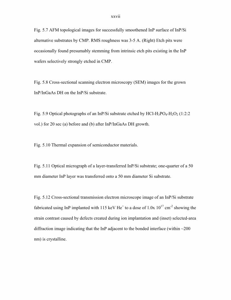
Fig. 5.7 AFM topological images for successfully smoothened InP surface of InP/Si
alternative substrates by CMP. RMS roughness was 3-5 A. (Right) Etch pits were
occasionally found presumably stemming from intrinsic etch pits existing in the InP
wafers selectively strongly etched in CMP.
Fig. 5.8 Cross-sectional scanning electron microscopy (SEM) images for the grown
InP/InGaAs DH on the InP/Si substrate.
Fig. 5.9 Optical photographs of an InP/Si substrate etched by HCl-H3PO4-H2O2 (1:2:2
vol.) for 20 sec (a) before and (b) after InP/InGaAs DH growth.
Fig. 5.10 Thermal expansion of semiconductor materials.
Fig. 5.11 Optical micrograph of a layer-transferred InP/Si substrate; one-quarter of a 50
mm diameter InP layer was transferred onto a 50 mm diameter Si substrate.
Fig. 5.12 Cross-sectional transmission electron microscope image of an InP/Si substrate
fabricated using InP implanted with 115 keV He+ to a dose of 1.0x 1017 cm-2 showing the
strain contrast caused by defects created during ion implantation and (inset) selected-area
diffraction image indicating that the InP adjacent to the bonded interface (within ~200
nm) is crystalline.

xxviii
Fig. 6.1 Schematic cross-sectional view of the InGaAs solar cell grown on the InP/Si
substrates.
Fig. 6.2 Optical micrographs of the InGaAs cells, including contact pads and grids,
fabricated on (left) an InP/Si substrate and (right) a bulk InP (001) substrate. The contact
pad on the left is the n-side contact and the pad on the right is the p-side contact.
Fig. 6.3 Optical micrograph of the InGaAs solar cells grown on an InP/Si substrate.
Fig. 6.4 Typical light I-V curves for the In0.53Ga0.47As solar cells grown on an InP/Si
substrate and on a commercial epi-ready InP substrate. The I-V measurements were
performed under AM1.5G illumination truncated at 850 nm.
Fig. 6.5 Measured spectral responses for the In0.53Ga0.47As solar cells grown on an InP/Si
substrate and on a commercial epi-ready InP substrate. The calculated absorbance of the
In0.53Ga0.47As layer for In0.53Ga0.47As/InP/SiO2/Si (solid line) and In0.53Ga0.47As/InP (dot
line) structures are also plotted.
Fig. 6.6 Calculated reflectivities of the InP/SiO2/Si and In0.53Ga0.47As/InP interfaces.
Fig. 7.1 Schematic for the trade-off issue in photovoltaic layer thickness. Thinner
photovoltaic layers will have less light absorption (left) while thicker layers will have
more bulk carrier recombination (right).
xxix
Fig. 7.2 Schematic cross-sectional of a solar cell structure with a back metal layer. The
incident light is incoupled into surface plasmons propagating at the semiconductor/metal
interface via subwavelength-size grooves to increase the optical path by switching the
light direction from normal to the photovoltaic layer to lateral.
Fig. 7.3 Schematic of the layer configuration considered for the energy dissipation
calculation.
Fig. 7.4 Calculated energy dissipation fraction in the semiconductor layer from the
surface plasmons propagating at the semiconductor/metal interface, depending on
incident photon energy (a) and wavelength (b).
Fig. 7.5 Schematic cross-sectional diagram of the optically thin GaAs solar cell structure.
Fig. 7.6 Scanning electron microscope (SEM) images of the Ag nanoparticle arrays with
a diameter of 60 nm and heights ranging through 10 nm to 75 nm deposited on the GaAs
solar cells with a viewing angle of 75 degree.
Fig. 7.7 Normalized photocurrent spectra for the GaAs solar cells with (a) Ag and (b) Al
nanoparticles. Computed normalized absorbance curves in the GaAs solar cells with Ag
and Al nanoparticles based on the optical model are also plotted.

xxx
Fig. 7.8 Straight optical transmission spectra of Ag nanoparticle arrays with a particle
diameter of 60 nm and various particle heights deposited onto glass substrates.
Fig. 7.9 Calculated radiation efficiency for Ag nanoparticles.
Fig. 7.10 (a) Normalized photocurrent and external quantum efficiency spectra and (b)
light I-V characteristics under AM1.5G 1-sun solar spectrum for the GaAs solar cells
with Ag nanoparticles with a diameter of 70 nm and height of 100 nm.
Fig. 7.11 Schematic cross-sectional diagrams of (a) the waveguide-like GaAs solar cell
with metal back layer, (b) the inversely grown GaAs solar cell used for the waveguide-
like cell structure and (c) the reference cell.
Fig. 7.12 Cross-sectional SEM image for the fabricated waveguide-like GaAs solar cell
with an Ag back layer. Note that a selective chemical etching was applied for the purpose
to clarify each layer.
Fig. 7.13 Photographs of (a) the waveguide-like GaAs solar cell with an Ag back layer
and (b) the reference cell with a 3 μm GaAs absorbing layer.
Fig. 7.14 (a) AFM and (b) SEM images of the surface of the InGaP BSF layer after
removal of the 3 μm thick GaAs layer, which represents the roughness at the GaAs cell /
Ag interface.
xxxi
Fig. 7.15 Typical light I-V curves for the waveguide-like GaAs cells with Ag back
structure and the reference GaAs cells under AM1.5 Global solar spectrum with 1-sun
total intensity (100 mW cm-2).
Fig. 7.16 Normalized photocurrent spectrum of the waveguide-like GaAs solar cell
relative to the photocurrent of the reference cell.
Fig. 7.17 Calculated dispersion relation at GaAs/Ag interface. Surface plasmon resonance
peak is found at 600 nm, represented by the maximum of the wavevector k parallel to the
interface.
Fig. 7.18 Calculated normalized absorbance for the waveguide-like GaAs solar cell
accounting Fabry-Perot resonance effect in the thin GaAs layer with the Ag back layer, as
well as the wavevector parallel to the GaAs/Ag interface shown in Figure 7.17,
superposed to the normalized photocurrent data in Figure 7.16.

xxxii
List of Tables
Table 5.1 List of the chemical solutions for InP smoothening used in this study. Agent 1,
2 and 3 are dissolver, oxidizer and diluent, respectively.

Chapter 1 Introduction
1-1. Global crisis and Solar cells
The current world’s consumption of electric energy is around 12-13 TW and the earth
receives more solar energy in 1 hour than is the energy used in 1 year globally,
considering the solar constant 1.7 x 10⁵ TW at the top of the earth’s atmosphere. [1]
However the solar energy incidence, around 1 kW/m2, is quite dilute and requires vast
area of energy converters to meet the world’s energy consumption. Therefore high
efficiency solar energy conversion is crucial. Solar cells, also called photovoltaics, are
devices converting the energy of the sunlight into electricity by the photovoltaic effect
discovered by the French scientist Henri Becquerel in 1839. Electron-hole pairs are
generated by the energy of the incident photons overcoming the energy bandgap of the
photovoltaic material to make a current flow according to the built-in potential slope,
typically with a p-n junction of semiconductor, in the material, as schematically depicted
in Figure 1.1. Solar cells have been recognized as an important alternative power source
especially since the 1970s oil crises. Solar cells are also promising as a carbon-free
energy source to suppress the global warming.
The energy conversion efficiency of a solar cell is defined as the ratio of the electric
power generated by the solar cell to the incident sunlight energy into the solar cell per
time. Currently the highest reported cell efficiencies in laboratories are around 40% while
the energy conversion efficiencies for thermal power generation can exceed 50%. This
fact however never means the superiority of thermal generation since its resources such
2
as fossil fuels are limited while the solar energy is essentially unlimited. The incident
energy flux spectrum of sunlight for reported solar cell efficiencies is standardized as
some specifically defined spectra such as Air Mass 0 (AM0), Air Mass 1.5 Global and
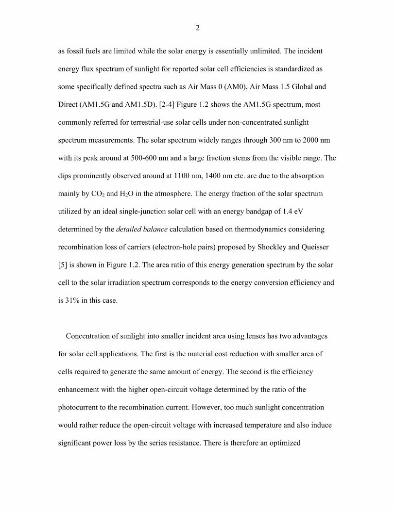
Direct (AM1.5G and AM1.5D). [2-4] Figure 1.2 shows the AM1.5G spectrum, most
commonly referred for terrestrial-use solar cells under non-concentrated sunlight
spectrum measurements. The solar spectrum widely ranges through 300 nm to 2000 nm
with its peak around at 500-600 nm and a large fraction stems from the visible range. The
dips prominently observed around at 1100 nm, 1400 nm etc. are due to the absorption
mainly by CO2 and H2O in the atmosphere. The energy fraction of the solar spectrum
utilized by an ideal single-junction solar cell with an energy bandgap of 1.4 eV
determined by the detailed balance calculation based on thermodynamics considering
recombination loss of carriers (electron-hole pairs) proposed by Shockley and Queisser
[5] is shown in Figure 1.2. The area ratio of this energy generation spectrum by the solar
cell to the solar irradiation spectrum corresponds to the energy conversion efficiency and
is 31% in this case.
Concentration of sunlight into smaller incident area using lenses has two advantages
for solar cell applications. The first is the material cost reduction with smaller area of
cells required to generate the same amount of energy. The second is the efficiency
enhancement with the higher open-circuit voltage determined by the ratio of the
photocurrent to the recombination current. However, too much sunlight concentration
would rather reduce the open-circuit voltage with increased temperature and also induce
significant power loss by the series resistance. There is therefore an optimized
3
concentration factor for each solar cell. Although this thesis will not discuss the detail of
concentrators, interested readers can refer Ref. 6-8.
Solar cells made of III-V semiconductor compounds have been exhibiting the leading
energy conversion efficiencies rather than the other materials represented by silicon. [9]
Besides the potential for high efficiency, III-V semiconductor compound materials have
advantages including the bandgap tunability by elemental compositions, higher photon
absorption by the direct bandgap energies, higher resistivity against high-energy rays in
space, and smaller efficiency degradation by heat than Si solar cells. The energy
conversion efficiencies of III-V solar cells are steadily increased year by year and
approaching 40% for the laboratory-scale cells as seen in Figure 1.3. [10] A lot of efforts
have been made to date to improve the cell performance further for the purpose of the
development of space activities and the solution for the upcoming energy crisis and
global environmental issues.
1-2. Developments of multijunction III-V semiconductor compound solar cells
Here I describe the principle, history and recent developments of multijunction III-V
solar cells in this section. One of the major factors of energy loss in a solar cell is the gap
between the photon energy and the bandgap energy of the photovoltaic material. No
absorption would occur if the photon energy was smaller than the bandgap energy and
merely the part equal to the bandgap energy out of the photon energy could be extracted
as electric power leaving the other part wasted as heat if larger. Multistacking of
photovoltaic materials of different bandgap energies is therefore commonly used for high

4
efficiency III-V solar cells to reduce this energy loss and absorb the photon energy from
the sunlight spectrum more widely and efficiently, taking advantage of the tunability of
bandgap energies and lattice constants with the compositions of III-V semiconductor
compounds, called multijunction or tandem cells. The theoretical efficiency limit based
on the detailed balance calculation estimated by Henry shows that a 36-gap or -junction
cell ideally could reach 72% efficiency at a concentration of 1000 suns relative to the
37% for a 1-gap cell. (Figure 1.4) [11] A theoretical calculation for the ideal efficiencies
according to the bandgap energy combinations of the top and bottom semiconductor
materials in two-junction (2J) solar cells are shown in Figure 1.5. [12] Similar
calculations under different conditions are found in Ref. 13 and 14.
For multijunction cells, monolithic or two-terminal structures are generally favored
and used rather than expensive and impractical three- or four-terminal structures. [15] A
schematic cross-sectional diagram of a monolithic 3J solar cell structure is shown in
Figure 1.6. [16] Multijunction solar cells have been layered by epitaxial growth generally
with metalorganic chemical vapor deposition (MOCVD) requiring lattice matching
among the stacked semiconductor materials. [17-20] Figures 1.7 and 1.8 show the
relation between the lattice constants and the bandgap energies for commonly used III-V
semiconductor compounds.
One of the most common and highest efficiency two 2J cells consists of a combination
of In0.48Ga0.52P and GaAs with the same lattice constant of 5.64 A and the bandgap
energy of 1.86 eV and 1.42 eV, respectively. [22-24] This InGaP/GaAs cell has the

5
highest efficiency of 30.3% under AM1.5G solar spectrum with 1-sun intensity (100 mW
cm-2) among monolithic 2J cells [9, 24], while 4-terminal configuration allowed the
highest 2J efficiency of 32.6% under AM1.5D spectrum at 100 suns for a lattice-
mismatched GaAs/GaSb stack (GaSb: 6.09 A, 0.70 eV). [25]
For 3J cells, most commonly so far, a Ge bottom cell is added to the InGaP/GaAs 2J cell
to form an InGaP/GaAs/Ge structure for Ge’s lattice constant of 5.66 A nearly equal to
that of InGaP/GaAs. This 3J structure is grown on a Ge substrate and an advantage that
Ge is a cheaper and mechanically stronger material than GaAs relative to cells grown on
GaAs substrates. The current formally-reported highest efficiency solar cell (as of May,
2008) is actually an InGaP/GaAs/Ge 3J cell with the efficiency of 40.7% at 240 suns
under AM1.5D. [26, 27] However, it should be noted that the 0.66 eV bandgap energy of
Ge is not optimal as the material for the bottom cell in a 3J cell. This point will be
discussed in the following section.
Specifically for the space use, very thin, light and flexible InGaP/GaAs 2J and
InGaP/GaAs/Ge 3J cells are being developed recently. [28-30] Figure 1.9 shows a
photograph of a flexible InGaP/GaAs 2J device. [30] Although the fabrication processes
have not been well disclosed, the photovoltaic layers are attached to metal or polymer
supporting films and the parent substrates for the epitaxial growth are removed somehow.
For further improvement of the cell efficiency, cells with more junctions are being
proposed such as an InGaP/GaAs/InGaAsN/Ge 4J structure. [31] Recently an
(Al)InGaP/InGaP/Al(In)GaAs/(In)GaAs/InGaAsN/Ge 6J cell has been demonstrated.
[32] The efficiency of this 6J cell was 23.6% under AM0 at 1 sun (135 mW cm-2). (Note

6
that the intensities of 1 sun for AM1.5 and AM0 are different. See Ref. 4 and 33 for the
detail of the standard artificial solar spectra for cell measurements.) This efficiency is
much lower than the highest efficiency 3J cell regardless of more number of junctions
presumably due to the current-limiting InGaAsN layer with low quantum efficiency. The
open-circuit voltage of this 6J cell was however 5.33V, significantly higher than the 3.09
V of the highest efficiency 3J cell, simply because of the series connection of six
semiconductor materials.
1-3. 1.0 eV bandgap subcells
Here I briefly review the fabrication and characteristics of the materials with bandgap
energies around 1.0 eV, one of the most critical issues for the further development of III-
V multijunction cells in the near future, in this section. The optimal bandgap energy for
the bottom cells in 3J solar cells is known to be around 1.0 eV considering the current
matching among three subcells, assuming the top two-junction structure is the
InGaP/GaAs. [34] Therefore materials of ~1.0 eV bandgap lattice-matched to GaAs and
Ge are intensively searched these days. As well as replacing the Ge subcell with a 1.0 eV
bandgap material, insertion of a 1.0 eV material between the GaAs and Ge subcells
would also improve the efficiency. Such a 4J cell could exhibit an efficiency higher than
50% theoretically. [35] It should be noted that another way to improve the efficiency
from the InGaP/GaAs/Ge 3J cell is to increase the bandgap of the InGaP subcell by
adding Al. However the addition of Al induces a significant reduction of the photocurrent
of the InGaP cell probably due to the adverse effect of Al and the associated oxygen
contamination on minority-carrier properties. [36] Lowering the bandgap of the GaAs
7
middle cell by substituting a portion of the Ga content with In is also a way for higher
efficiency than the InGaP/GaAs/Ge 3J cell, although this approach accompanies lattice
mismatch and requires graded buffer layers or suffers from large density of dislocations
otherwise. [37, 38]
InxGa1-xAs1-yNy can be lattice matched to GaAs for compositions satisfying x = 3y and
can have a bandgap of ~1.0 eV. [39] Although this InGaAsN has been thought to be the
most promising candidate, its minority carrier diffusion length has been too short
resulting low output photocurrent. [40-42] Other candidates such as ZnGeAs2, GaTlP2
and InGaAsB have not shown very promising properties either. [15]
Sb has been recently incorporated in the nitride system to form InGaAsNSb cells lattice-
matched to GaAs with 0.92 eV bandgap and demonstrated relatively high quantum
efficiency and current density enough for current-matching to the InGaP/GaAs cell. [43]
The open-circuit voltage was however quite low and it is unclear if this InGaAsNSb
would be better than Ge.
An alternative is a 1.0 eV InGaAs material lattice-mismatched to GaAs with graded
compositions in epitaxial growth. [44] A ~1 eV InGaAs subcell lattice-mismatched to
GaAs by 2.2% was grown on an inversely grown GaAs/InGaP 2J subcell via transparent
compositionally graded layers. This epitaxial structure was mounted to a pre-metallized
Si supporting wafer and then the parent GaAs substrate was selectively removed resulting
an InGaP/GaAs/InGaAs 3J cell. This inversely grown cell achieved a 38.9% efficiency
8
under AM1.5D at 81 suns and also the highest efficiency (as of May, 2008) for AM1.5G,
1-sun condition of 33.8%. [45-47]
1-4. Outline of Thesis
In this chapter I described the importance of the photovoltaic devices or solar cells, the
motivation of this study. In Chapter 2, I will introduce the wafer bonding technologies
and their applications. In Chapter 3, I will describe my experiment for wafer bonding of
GaAs and InP wafers as a preparation of the direct-bonded multijunction solar cells. In
Chapter 4, the fabrication and characterization of lattice-mismatched GaAs/InGaAs solar
cells via direct wafer bonding technique will be shown. In Chapter 5, the introduction and
experiments for InP layer transfer onto Si for III-V solar cell cost reduction will be given.
In Chapter 6, the fabrication and characterization of InGaAs solar cells grown on the
prepared layer-transferred InP/Si low-cost alternative epitaxial substrates will be
described. In Chapter 7, the development of GaAs “plasmonic” solar cells with metallic
nanostructures for absorption enhancement will be described. This thesis will end with
Chapter 8, conclusions and future outlook.
1-5. References
[1] A. J. Nozik, Inorg. Chem. 44, 6893 (2005).
[2] K. Emery and C. Osterwald, Sol. Cells 17, 253 (1986).
[3] S. Nann and K. Emery, Sol. Energy Mater. 27, 189 (1992).
[4] K. Emery, in Handbook of Photovoltaic Science and Engineering, edited by A. Luque
and S. Hegedus (Wiley, New York), Chap. 16 (2003).
9
[5] W. Shockley and H. J. Queisser, J. Appl. Phys. 32, 510 (1961).
[6] P. Campbell and M. A. Green, IEEE Trans. Electron. Dev. 33, 234 (1986).
[7] V. Andreev et al, Photovoltaic Conversion of Concentrated Sunlight (Wiley, New
York) (1997).
[8] R. M. Swanson, in Handbook of Photovoltaic Science and Engineering, edited by A.
Luque and S. Hegedus (Wiley, New York), Chap. 11 (2003).
[9] M. A. Green et al, Prog. Photovolt. Res. Appl. 13, 387 (2005).
[10] T. Surek, J. Cryst. Growth 275, 292 (2005).
[11] C. H. Henry, J. Appl. Phys. 51, 4494 (1980).
[12] H. Takakura, Jpn. J. Appl. Phys. 31, 2394 (1992).
[13] S. R. Kurtz et al, J. Appl. Phys. 68, 1890 (1990).
[14] A. W. Bett et al, Appl. Phys. A 69, 119 (1999).
[15] J. M. Olson et al, in Handbook of Photovoltaic Science and Engineering, edited by
A. Luque and S. Hegedus (Wiley, New York), Chap. 9 (2003).
[16] K. Nishioka et al, Jpn. J. Appl. Phys. 43, 882 (2004).
[17] M. Sugo et al, J. Appl. Phys. 68, 540 (1990).
[18] R. D. Dupuis, IEEE J. Select. Top. Quant. Elect. 6, 1040 (2000).
[19] Y. Shimizu and Y. Okada, J. Cryst. Growth 265, 99 (2004).
[20] Y. Li et al, Phil. Mag. 85, 3073 (2005).
[21] S. Tiwari and D. J. Frank, Appl. Phys. Lett. 60, 630 (1992).
[22] J. M. Olson et al, Appl. Phys. Lett. 56, 623 (1990).
[23] K. A. Bertness et al, Appl. Phys. Lett. 65, 989 (1994).
[24] T. Takamoto et al, Appl. Phys. Lett. 70, 381 (1997).
10
[25] L. M. Fraas et al, Proc. 21st IEEE Photovoltaic Specialists Conference, Kissimimee,
190 (1990).
[26] R. R. King et al, Proc. 4th International Conference on Solar Concentrator, El
Escorial (2007).
[27] R. R. King et al, Appl. Phys. Lett. 90, 183516 (2007).
[28] T. Takamoto et al, Proc. 31st IEEE Photovoltaic Specialists Conference, Lake
Buena Vista, 519 (2005).
[29] D. C. Law et al, Proc. IEEE 4th World Conference on Photovoltaic Energy
Conversion, Waikoloa, 1879 (2006).
[30] T. Takamoto et al, Proc. IEEE 4th World Conference on Photovoltaic Energy
Conversion, Waikoloa, 1769 (2006).
[31] N. H. Karam et al, Sol. Ener. Mater. Sol. Cell. 66, 453 (2001).
[32] R. R. King et al, Proc. IEEE 4th World Conference on Photovoltaic Energy
Conversion, Waikoloa, 1757 (2006).
[33] D. R. Myers et al, Proc. 28th IEEE Photovoltaic Specialists Conference, Anchorage,
1202 (2000).
[34] D. J. Friedman et al, Proc. IEEE 2nd World Conference on Photovoltaic Energy
Conversion, Vienna, 3 (1998).
[35] S. R. Kurtz et al, Proc. 26th IEEE Photovoltaic Specialists Conference, Anaheim,
875 (1997).
[36] R. R. King et al, Proc. 28th IEEE Photovoltaic Specialists Conference, Anchorage,
998 (2000).
11
[37] R. R. King et al, Proc. IEEE 4th World Conference on Photovoltaic Energy
Conversion, Waikoloa, 760 (2006).
[38] F. Dimroth et al, IEEE Electron. Dev. Lett. 21, 209 (2000).
[39] M. Kondow et al, Jpn. J. Appl. Phys. 35, 1273 (1996).
[40] J. F. Geisz et al, J. Cryst. Growth 195, 401 (1998).
[41] D. J. Friedman et al, J. Cryst. Growth 195, 409 (1998).
[42] S. R. Kurtz et al, Appl. Phys. Lett. 74, 729 (1999).
[43] D. B. Jackrel et al, J. Appl. Phys. 101, 114916 (2007).
[44] M. W. Wanlass et al, Proc. 31st IEEE Photovoltaic Specialists Conference, Lake
Buena Vista, 530 (2005).
[45] M. W. Wanlass et al, Proc. International Conference on Solar Concentrators for the
Generation of Electricity or Hydrogen, Scottsdale (2005).
[46] M. W. Wanlass et al, Proc. IEEE 4th World Conference on Photovoltaic Energy
Conversion, Waikoloa, 729 (2006).
[47] J. F. Geisz et al, Appl. Phys. Lett. 91, 023502 (2007).

12
Fig. 1.1 Schematic diagram of the work principle of photovoltaic devices or solar cells.
Electrical current is generated from charge carriers (electrons and holes) excited by
incident light flowing directed by the potential slope built by a p-n junction in a
semiconductor.
13
Fig. 1.2 Solar irradiation spectrum of AM1.5G and energy utilization spectrum by a
single-junction solar cell with an energy bandgap of 1.4 eV.

14
Fig. 1.3 Chronological record energy-conversion efficiencies of solar cells. (from Ref.
10)

15
Fig. 1.4 Graphical analysis of the efficiencies of 1, 2, 3 and 36 energy gap solar cells. The
step heights equal to the photon flux absorbed, nph, by each energy gap and the step
widths (measured from the origin) equal to the maximum energy per absorbed photon,
delivered to the load. The efficiency of each cell is given by the ratio of the area enclosed
by steps and the area under the outer curve, labeled 100%. (from Ref. 11)

16
Fig. 1.5 Calculated isoefficiency map for two-junction four-terminal solar cells under
AM1.5G spectrum at one-sun illumination according to the top and bottom cell bandgaps.
(from Ref. 12)

17
Fig. 1.6 Cross-sectional schematic of a three-junction cell structure. (from Ref. 16)

18
0.0
0.5
1.0
1.5
2.0
2.5
3.0
5.2 5.4 5.6 5.8 6.0 6.2 6.4 6.6
Lattice constant (A)
Ban
dgap
ene
rgy
(eV
)
GaAs
GaP
InP
AlP
GaSb
AlSb
AlAs
Ge
InAs InSb
Si
0.0
0.5
1.0
1.5
2.0
2.5
3.0
5.2 5.4 5.6 5.8 6.0 6.2 6.4 6.6
Lattice constant (A)
Ban
dgap
ene
rgy
(eV
)
GaAs
GaP
InP
AlP
GaSb
AlSb
AlAs
Ge
InAs InSb
Si
Fig. 1.7 Bandgap energies plotted as a function of the lattice constant of semiconductors.
19
Fig. 1.8 Conduction band edge and valence band edge energies plotted as a function of
the lattice constant of semiconductors. The zero energy point represents the approximate
gold Schottky barrier position in the band gap of any given alloy. (from Ref. 21)

20
Fig. 1.9 Photograph of a flexible thin-film InGaP/GaAs two-junction 4x7-cm2 film-
laminated cell. (from Ref. 30)

21
Chapter 2 Wafer bonding for solar cell applications
2-1. Introduction
In the previous chapter, multijunction solar cells for high efficiency energy conversion
were introduced. In this chapter, we will look into more detail or learn what kind of
materials stacking would make multijunction solar cells more efficient. To do that, we
use the “detailed balance limit calculation”, a method to estimate the thermodynamical
limit of solar energy conversion, to determine ideal bandgap combinations. We will
recognize that release of the lattice matching restriction among the stacking materials
would give us significant improvement of efficiency. As a way to overcome the lattice
mismatch, the wafer bonding technique is introduced as a method to stack semiconductor
materials compared with the conventional epitaxial growth.
2-2. Ideal lattice-mismatched multijunction solar cells, detailed balance limit
calculation
In the previous chapter, I mentioned multijunction solar cells can exhibit higher energy
conversion efficiencies rather than single-junction cells. In this section, let’s estimate
what kind of combinations of semiconductor materials with bandgap energies can ideally
achieve how much energy conversion efficiencies. To do that, here I will use the
“detailed balance limit” calculation method developed by Shockley and Queisser. [1] The
“detailed balance limit” represents the thermodynamical energy conversion efficiency
limit of solar cells taking black-body radiation into account. See References 1 and 2 for
the detail of the theory and formalism. The radiative current density Jrad can be written as

22
∫∫ Ω=∞
gradEcrad vddeJ θρω cos/ h
, (Eq. 1)
where the radiation density ρrad is given by
⎟⎠⎞
⎜⎝⎛ −
≅kT
eVvk
grad
ωπ
ρ hexp41 2
. (Eq. 2)
T represents the temperature of the solar cell and was assumed to be 300 K in this Thesis,
as in References 1 and 2. Considering the total reflection at the top surface of the active
region, the angular integral in Eq. 1 becomes
(∫ +=Ω 2/11cos nd πθ ), (Eq. 3)
where n is the refractive index of the active region, and Jrad becomes
( )⎟⎟⎠
⎞⎜⎜⎝
⎛ −≅⎟
⎠⎞
⎜⎝⎛ −+
= ∫∞
kTEeV
AdkT
eVc
neJ g
Ecrad expexp4
1/
222
2
ωωωπ
hh
, (Eq. 4)
where
( )232
22
41
ckTEne
A g
hπ+
≡ . (Eq. 5)

23
The current density to the load is
⎟⎟⎠
⎞⎜⎜⎝
⎛ −−=−≅
kTEeV
AJJJJ gphradph exp , (Eq. 6)
where Jph is the carrier generation flux and
( ) ( ) λλλ dIQJ Sph ∫= , (Eq. 7)
where
)()(
λλ
S
g
EE
Q = ( )( )gS EE ≥λ
0= ( )( )gS EE <λ , (Eq. 8)
where λ is the corresponding wavelength of sunlight, IS (λ) is the incident energy flux
density of the solar irradiation, the energy utilization factor Q (λ) is the fraction of the
incident energy flux used to excite electron-hole pairs, Eg is the energy bandgap of the
solar cell material, and ES (λ) = hν is the energy of the photons with the wavelength of λ.
Setting J = 0 in Eq. 6, the open-circuit voltage is

24
⎟⎟⎠
⎞⎜⎜⎝
⎛−=
phgoc J
AkTEeV ln . (Eq. 9)
The voltage at the maximum power point is found by setting the derivative d(JV)/dV = 0.
⎟⎠⎞
⎜⎝⎛ +−=
kTeVkTeVeV m
ocm 1ln (Eq. 10)
Solving this transcendental equation for Vm, the current density at the maximum power
point, Jm, is obtained by
m
phm eVkT
JJ
/1+= . (Eq. 11)
Finally the solar cell efficiencies are calculated by
( ) λλη
dIVJ
S
mm
∫= . (Eq. 12)
Air Mass 1.5 Global solar spectrum (AM1.5G) was used as IS (λ) for the cases of 1-sun
irradiation intensity. Air Mass 1.5 Direct solar spectrum (AM1.5D) was used for
concentration cases considering only direct incidence of the sunlight, not scattered
photons, as appropriate for optical concentrators.

25
Figure 2.1 shows the solar irradiation spectrum, IS (λ), and the calculated energy
utilization spectrum by a single-junction solar cell with the optimized Eg to maximize η
under 1-sun and concentration illumination. Ratio of the integral of the energy utilization
spectrum for the solar cell to the integral of the solar irradiation spectrum corresponds to
the energy conversion efficiency, η, of the solar cell. The obtained η for the cell, 31.3%
for 1 sun and 37.6% for 1000 suns, are quite consistent with the results presented in Ref.
1 and 2.
Figure 2.2 shows an example of the solar irradiation spectrum, IS (λ), and the calculated
energy utilization spectrum by a four-junction solar cell for 1-sun illumination. The
bandgap energies were randomly picked and current matching among subcells was not
considered here. Again, note that the ratio of the integral of the energy utilization
spectrum for the solar cell to the integral of the solar irradiation spectrum corresponds to
the energy conversion efficiency, η, of the solar cell. In this four-junction cell case, η
reaches ~50%. We see here that multijunction solar cells can collect solar energy more
efficiently than single-junction cells do.
First, I investigated (Al)InGaP/GaAs/3rd subcell triple junction solar cells since
In0.5Ga0.5P/GaAs dual-junction (2J) cells are known to be the most efficient monolithic 2J
cells, as I described in the previous chapter. Figure 2.3 shows the dependence of the
computed detailed balance limit efficiency on the bandgap energy of the 3rd subcell under
a 100-sun illumination. It is found that as the bandgap energy of the bottom subcell goes
up, the efficiency could go even higher than the case of Ge, because of higher

26
photovoltage while the photocurrent is limited by the top subcells. The calculated
detailed balance limit efficiency reaches 50.5% with a 3rd subcell with a bandgap energy
of 1.02 eV, relative to 45.6% with a Ge 3rd subcell. Note again that the current (as of May,
2008) solar cell efficiency record is 40.7% with an InGaP/GaAs/Ge triple-junction cell
under a 240-sun illimination. [3]
Furthermore, if we could make a (Al)InGaP/GaAs/3rd subcell/4th subcell four-junction
solar cell, the efficiency could be even higher. Figure 2.4 shows a contour plot of four-
junction cell efficiencies depending on the bandgap energies of the 3rd and 4th subcells.
[4] We see that certain combination of the bandgap energies of the bottom two subcells
would lead up to ~55% efficiency. Given a 4th subcell of In0.53Ga0.47As lattice matched to
InP (Eg = 0.74 eV), I calculated the maximum efficiency to be 51.4% with the optimized
3rd subcell bandgap energy of 1.06 eV.
So far we only have looked at series connection, but the calculated maximum efficiency
reaches 55.7%, as shown in Figure 2.5, for the same (Al)InGaP/GaAs/3rd subcell/InGaAs
four-junction solar cell with the optimized 3rd subcell bandgap energy of 1.06 eV
assuming independent connection of the top dual-junction and the bottom dual-junction.
However, it is not trivial to fabricate these types of triple or four-junction III-V
semiconductor compound solar cells due to the issue of lattice mismatch among materials.
Figure 2.6 shows a plot of lattice constants and bandgap energies for commonly used III-
V semiconductor compounds, which specifically shows a lattice mismatch between top

27
subcells such as (Al)InGaP and GaAs and bottom subcells such as InGaAsP and InGaAs.
Figure 2.7 shows cross-sectional transmission electron microscopy (TEM) images for the
interface of grown layers and substrates with lattice mismatch for common III-V
semiconductor compound materials. [5, 6] These images indicate that even a lattice
mismatch of a couple of percent generates a significant density of threading dislocations,
which would degrade the performance of photovoltaic devices by acting as carrier
recombination centers.
2-3. Wafer bonding technology for solar cell applications
2-3-1. What is wafer bonding ?
Wafer bonding is a technique to form a homo- or hetero-junction by bonding two
materials. There are two types of wafer bonding schemes. One is direct wafer bonding
with no additional bonding layer between the two materials you want to get together. The
other is bonding via some bonding layers such as semiconductor oxides, metals or
adhesive polymers to enhance the bonding strength. To the best of my knowledge, direct
wafer bonding was first proposed and demonstrated by Shimbo et al [7] as a method to
form an abrupt p-n junction of silicon diode. They joined two mirror-polished Si wafers
and annealed the pairs to found that the bonding interfacial strength increases with
increasing temperature at above 300 oC to reach a fracture strength of bulk silicon (100 -
200 kg/cm2) at 1000 oC.
Presence of dislocations brings us undesirable effects on electronic performance of
semiconductor materials, serving as easy diffusion paths for dopants or as recombination

28
centers to diminish carrier density in devices. [8] Therefore, controlling structural defects
by misfit strain is an important issue.
Wafer bonding, which makes a heterostructure from a pair of crystalline wafers, can
avoid threading dislocations confining all of the dislocations at the heterointerface.
Because only the atoms very close to the interface participate in the reaction, the rest of
the material is not affected by the bonding process and no defects can propagate into the
layers. In other words, we can operate a wafer bonding process at a temperature where
covalent bonds across the heterointerface form but the thermal fluctuation cannot
overcome the kinetic barrier for the advance of threading dislocations. Somehow low
temperature does not allow strain relaxation by generation of threading dislocations
which is thermodynamically preferred, but leaves the structure at a metastable state.
2-3-2. Mechanics in wafer bonding
Wafer bonding, which makes a heterostructure from a pair of crystalline wafers, can
avoid threading dislocations confining all of the dislocations at the heterointerface.
Because only the atoms very close to the interface participate in the reaction, the rest of
the material is not affected by the bonding process and no defects can propagate into the
layers. In other words, we can operate a wafer bonding process at a temperature where
covalent bonds across the heterointerface form but the thermal fluctuation cannot
overcome the kinetic barrier for the advance of threading dislocations. Somehow low
temperature does not allow strain relaxation by generation of threading dislocations
which is thermodynamically preferred, but leaves the structure at a metastable state.

29
The transition between coherency (with no dislocation and with strain) and semi-
coherency (strain is partially relaxed by dislocations) also requires the motion of
dislocations to (or near to) the epilayer/substrate interface, not only the discussion on
energy we have done above.
Considering the Peach-Koehler force,
^lbFd ×⎟
⎠⎞
⎜⎝⎛ •=
=−−
σ , (Eq. 13)
which describes the force acting on unit length of dislocation in an external stress field,
and from a similar formalism as the total energy by strain and dislocations, ucoh + udis, we
derived above, the excess force to drive the bending of threading dislocations to form
misfit segments is;
( ) ⎟⎠⎞
⎜⎝⎛
⎟⎟⎠
⎞⎜⎜⎝
⎛−
−−−⎟
⎠⎞
⎜⎝⎛
−+
−=
−=
bh
hbbf edgmd
discohexc
4ln1
cos1cos41
122
||, νβν
λπμρ
ννμ
σσσ (Eq. 14)
When σexc > 0, threading dislocations will tend to bend over to form strain-relaxing misfit
segments. When σexc < 0, threading dislocations that have bent over to form strain-
relaxing misfit segments will tend to straighten. [9-11]

30
Based on the excess stress, a measure of the driving force for strain relaxation by
dislocation creation, the dynamics of dislocations in bulk materials is summarized in
what are known as deformation-mechanism maps, hereafter denoted as DMM. Figures
2.8 and 2.9 are the DMM for Si and Ge, respectively. [12] From the iso-strain rate
contours in the maps, we can roughly estimate the dislocation density in the material for a
given set of stress, process temperature and time.
Let’s think about wafer bonding of Si and Ge as a case study. From Eq. 14, the
normalized stress, σ/μ, at the bonding heterointerface is around or less than the misfit, f,
which is 4 % for Si and Ge. This is because the Poisson’s ratio, v, is around 0.25 – 0.35
for most common materials and then 2(1-ν)/(1+ν) is around 1. Then, in Figures 2.8 and
2.9, the strain rate drastically varies between 1x10⁻¹⁰ s-1 and 1 s-1 for both of Si and Ge
around at half of their melting temperature, at which people actually do the wafer
bonding successfully.
However, stress depends on the position in the layers from the interface. A theoretical
model considering periodic compressive and tensile strains along the wafer-bonded
interface shows that the strain is highly localized to the interface rapidly diminishing
away from the interface. [13] The displacement of atoms to the direction parallel to the
bonding interface is proportional to an exponent including the distance from the interface;
⎟⎠⎞
⎜⎝⎛−∝ z
afExpu π2 ,
31
where f is the lattice mismatch, a is the lattice constant, and z is the distance from the
interface. From this equation, assuming f = 0.05 and a = 5 A, the atomic displacement at
the 10 nm distant from the interface is only 0.2 % of that of the interface. Since stress is
proportional to displacement, σ/μ is less than 1x10⁻⁴ at 10 nm distant from the interface in
this case, where the strain rate is far smaller than 1x10⁻¹⁰ s-1 in the DMM. At this strain
rate, the dislocation density is less than the order of one dislocation per centimeter, which
is essentially negligible, after 1 hour thermal process. This implies a minimal disturbance
to the bulk of the materials during the wafer bonding process.
Actually a lot of TEM observations show only misfit dislocations at the bonded
interface, sometimes with threading dislocation half-loops around the interface, but no
threading dislocation throughout a layer. [14]
This is rather different from the heteroepitaxial growth of thick layers on lattice-
mismatched substrates, in which the strain relaxation resulted in high densities of
threading dislocations in the grown layers. When growth proceeds, many of misfit
dislocations at the interface continue to extend into the thickness of the grown structure.
Since it is known that thermal strain from difference of thermal expansion coefficients is
proportional to the square root of layer thickness, it is often effective to thin one of the
bonded wafers before thermal process to reduce strain, if the interface has enough
mechanical strength to endure the thinning process. [14]

32
In equilibrium, theoretically the dislocation density in epi-grown films and wafer
bonded films would be same, as long as the combinations of the materials are same.
However, in wafer bonding, considering kinetics, the dislocations first generating at the
bonding interface cannot fully propagate throughout the films or mostly stay at the
interface leaving strain energy in the films, for common wafer bonding conditions
(temperature, time). So, we can conclude wafer-bonded heterostructures have
dislocations almost only at the bonded interfaces and therefore have better performance
as optoelectronic materials than those of epi-grown heterostructures, which have
dislocation also in the bulk region of the grown films.
Practically it is difficult to have the density of threading dislocation in heteroepitaxy less
than 1x106 cm-2. Under this defect density, most majority-carrier devices such as field-
effect transistors perform normally, but the minority-carrier devices such as lasers
experience appreciable degradation.
In contrast to the heteroepitaxial growth, these misfit dislocations were all edge
dislocations, strictly confined at the heterointerface. Neither stacking faults nor threading
dislocations were found over the entire region being inspected. [15-17]
2-3-3. Existing applications of wafer bonding
Direct wafer bonding of InP and GaAs is a significant and promising process for various
kinds of device application, such as high-speed LED and HEMT [18], long-wavelength
VCSEL [19], nano photonic crystals for WDM [20,21] and strained SiGe-on-insulator for

33
MOSFET [22]. Recently silicon-based (i.e. compatible with conventional CMOS
(complementary metal oxide semiconductor) technologies) hybrid InP laser was
developed using InP/Si wafer bonding by the team of Prof. John Bower of UC Santa
Barbara. [23] James Zahler et al, one of my collaborators, of Aonex Technologies has
succeeded to fabricate GaN LEDs on inexpensive wafer bonded sapphire/poly-AlN
substrates. [24]
2-3-4. Wafer bonding for lattice-mismatched multijunction solar cells
As we saw in the previous sections, multijunction solar cells with III-V semiconductor
compound materials are promising for ultrahigh (> 40%) efficiency solar energy
conversion in the coming decades. Most current multijunction solar cell design
approaches are focused on either lattice-matched designs or metamorphic growth with
dislocations to accommodate subcell lattice mismatch, which inevitably results in less
design flexibility or lower material quality than is desirable. [8, 25]
Material integration by the direct wafer bonding technique enable atomic scale
semiconductor- semiconductor bonding and do not utilize any metal as bonding agent at
interfaces. Thus interface transparency, thermal conductivity, thermal stability and
reliability should be superior to mechanical stacking approaches using patterned metallic
pastes and frits. Also, monolithic, or two-terminal, devices can be integrated into
modules with the same simplicity afforded by single-junction devices, with metallization
at the very top and bottom of the stack only. Three- and four-terminal configurations do
not require lattice mismatch or current matching. However, they are generally less

34
desirable structures, because of their complexities of fabrication and assembly, than the
monolithic device. [26]
Direct wafer bonding enables dislocation-free active regions by confining the defect
network needed for lattice mismatch accommodation to heterointerfaces. [14,27] The
strain is highly localized to the interface rapidly diminishing away from the interface,
implying a minimal disturbance to the bulk of the materials during the wafer bonding
process. [13]
Figure 2.10 shows an ideal structure of III-V multijunction solar cell, which could
exhibit ultrahigh efficiency. [28,29] It is difficult to prepare this multistack structure by
epitaxial growth with optimal material quality because of the 4% lattice mismatch across
the interface of the GaAs and InGaAs subcells. Wanlass et al reported a 37.9%
efficiency cell with an epitaxially grown triple-junction structure of InGaP/GaAs/InGaAs.
[30] However a considerable density of dislocations limiting the cell efficiency was
observed in the InGaAs layer of graded composition. This result suggests the potential of
over-40% efficiency utilizing the wafer bonding technology to diminish the dislocations.
In this thesis (Chapters 3 and4), GaAs/InP direct wafer bonding was first investigated
for mechanically robust and highly conductive heterointerfaces applicable for solar cell
applications. Secondly the first direct-bond interconnected multijunction solar cell, a
two-terminal monolithic GaAs/InGaAs dual-junction cell, was fabricated based on the
35
bonding investigation to demonstrate a proof-of-principle for the viability of direct wafer
bonding for solar cell applications.
2-3-5. Wafer bonding for III-V semiconductor compounds layer transfer for
inexpensive alternative epitaxial substrate structures
Wafer bonding technologies introduced in the previous sections can be applied not only
for lattice-mismatched stacking, but also for fabrication of low-cost epitaxial substrates.
Wafer bonding enables us to do “layer-transfer” of thin films of expensive III-V
semiconductor compound materials onto cheaper material substrates. This technique is
the second main topic of my thesis and its detail will be described in Chapters 5 and 6.
The basic idea is to reduce the cost of expensive InP bulk substrate for III-V
semiconductor compound multijunction solar cells by replacing those substrates with an
alternative substrate structure of a thin InP film sitting on top of an inexpensive Si wafer
(Figure 2.11), which can be fabricated through layer transfer technique using wafer
bonding.
2-4. List of symbols
ν: Poisson’s ratio (= the negative of the ratio between lateral and longitudinal strains
under uniaxial longitudinal stress)
μ: shear modulus (= the ratio between applied shear stress and shear strain under pure
shear)
b: Burgers vector
r0: inner radius of the cylinder, or the “cutoff” radius

36
R: outer radius of the cylinder
β: angle between the Burgers vector and the dislocation line
ρmd: linear density of dislocations
f: lattice parameter misfit between the epitaxial layer and the substrate
λ: angle between the Burgers vector and the direction that is both normal to the
dislocation line and that lies within the plane of the interface
h: thickness of the film
Uedg: energy per unit length associated with the elastic stresses and strains for edge
dislocations
Uscr: energy per unit length associated with the elastic stresses and strains for screw
dislocations
σ: stress
l: dislocation line
θ: twist angle between the wafer pairs
Sd: spacing between neighboring dislocations
a: lattice constant
Ddis: areal density of dislocations
2-5. References
[1] W. Shockley and H. J. Queisser, J. Appl. Phys. 32 (3), 510-519, 1961.
[2] C. H. Henry, J. Appl. Phys. 51 (8), 4494–4500, 1980.
[3] R. R. King et al, Appl. Phys. Lett. 90, 183516, 2007.
[4] J. M. Zahler, Doctoral Thesis, California Institute of Technology, 2005.\

37
[5] Y. Li et al, Phil. Mag. 85, 3073, 2005.
[6] P. Kongjaeng et al, J. Cryst. Growth 298, 111, 2007.
[7] M. Shimbo, K. Furukawa, K. Fukuda, and K. Tanzawa, J. Appl. Phys. 60, 2987-2989
(1986).
[8] S. Mahajan, Acta Mater. 48, 137-149, 2000.
[9] D. Hull, Introduction to Dislocations, 2nd ed., Pergamon Press, 1975.
[10] J. Y. Tsao, Materials Fundamentals of Molecular Beam Epitaxy, Academic Press,
1993.
[11] L. B. Freund and S. Suresh, Thin Film Materials –Stress, Defect Formation and
Surface Evolution, Cambridge University Press, 2003.
[12] H. J. Frost and M. F. Ashby, Deformation-Mechanism Maps, Pergamon, Oxford,
1982.
[13] Z. L. Liau. Phys. Rev. B 55 (19), 12899, 1997.
[14] U. Goesele and Q. Y. Tong, Ann. Rev. Mater. Sci. 28, 215, 1998.
[15] G. Patriarche et al, J. Appl. Phys. 82 (10), 4892-4903, 1997.
[16] Y. H. Lo et al, Appl. Phys. Lett. 58, 1961, 1991.
[17] Y. H. Lo et al, Appl. Phys. Lett. 62, 1038, 1993.
[18] T. Whitaker, Compound Semiconductor 35, May, 2002.
[19] H. C. Lin et al, J. Appl. Phys. 92, 4132, 2002.
[20] S. Noda et al, Appl. Phys. Lett. 75, 905, 1999.
[21] S. Noda et al, Science 289, 604-606, 2000.
[22] B. Ghyselen et al, Solid-St. Electron. 48, 1285, 2004.
[23] H. Park et al, Opt. Express 13, 9460, 2005.

38
[24] J. M. Zahler et al, Compound Semiconductor, Nov. 2006.
[25] Y. Shimizu and Y. Okada, J. Cryst. Growth 265, 99-106, 2004.
[26] J. M. Olson, D. J. Friedman, and S. R. Kurtz, in Handbook of Photovoltaic Science
and Engineering, edited by A. Luque and S. Hegedus (Wiley, New York), 2003, pp. 359-
411.
[27] A. Fontcuberta i Morral et al, Appl. Phys. Lett. 83, 5413-5415, 2003.
[28] J. M. Zahler et al, Proc. 29th IEEE Photovoltaic Specialists Conference, 45-48, 2002.
[29] P. R. Sharps et al, Proc. 26th IEEE Photovoltaic Specialists Conference, 895-
898,1997.
[30] M. W. Wanlass et al, MWW 3rd ISCC, 2005.

39
0 500 1000 1500 2000 2500 30000.0
0.2
0.4
0.6
0.8
1.0
1.2
1.4
1.6
1.8
Ener
gy fl
ux d
ensi
ty (W
/m2 /n
m)
Wavelength (nm)
1sun, AM1.5G solar irradiation Solar cell, Eg=1.4eV
Fig. 2.1 (a) Solar irradiation spectrum of AM1.5G, 1 sun and energy utilization spectrum
by a single-junction solar cell with the optimized energy bandgap to obtain the maximum
efficiency. Eg = 1.4 eV, η = 31.3%.
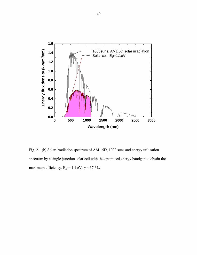
40
0 500 1000 1500 2000 2500 30000.0
0.2
0.4
0.6
0.8
1.0
1.2
1.4
1.6
Ener
gy fl
ux d
ensi
ty (k
W/m
2 /nm
)
Wavelength (nm)
1000suns, AM1.5D solar irradiation Solar cell, Eg=1.1eV
Fig. 2.1 (b) Solar irradiation spectrum of AM1.5D, 1000 suns and energy utilization
spectrum by a single-junction solar cell with the optimized energy bandgap to obtain the
maximum efficiency. Eg = 1.1 eV, η = 37.6%.
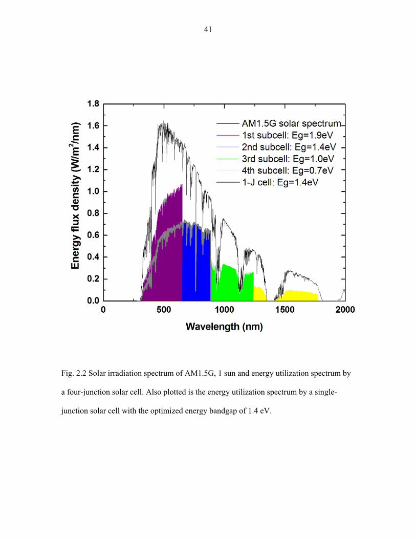
41
Fig. 2.2 Solar irradiation spectrum of AM1.5G, 1 sun and energy utilization spectrum by
a four-junction solar cell. Also plotted is the energy utilization spectrum by a single-
junction solar cell with the optimized energy bandgap of 1.4 eV.
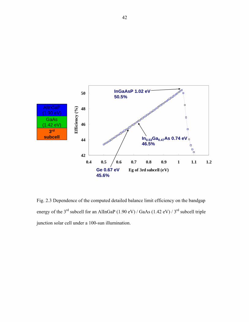
42
42
44
46
48
50
0.4 0.5 0.6 0.7 0.8 0.9 1 1.1 1.2
Eg of 3rd subcell (eV)
Effic
ienc
y (%
)
GaAs(1.42 eV)
3rd
subcell
AlInGaP(1.90 eV)
Ge 0.67 eV45.6%
In0.53Ga0.47As 0.74 eV46.5%
InGaAsP 1.02 eV50.5%
42
44
46
48
50
0.4 0.5 0.6 0.7 0.8 0.9 1 1.1 1.2
Eg of 3rd subcell (eV)
Effic
ienc
y (%
)
GaAs(1.42 eV)
3rd
subcell
AlInGaP(1.90 eV)
Ge 0.67 eV45.6%
In0.53Ga0.47As 0.74 eV46.5%
InGaAsP 1.02 eV50.5%
Fig. 2.3 Dependence of the computed detailed balance limit efficiency on the bandgap
energy of the 3rd subcell for an AlInGaP (1.90 eV) / GaAs (1.42 eV) / 3rd subcell triple
junction solar cell under a 100-sun illumination.

43
0.52
0.50
0.45 0.40
0.35
0.30
0.54
0.25
0.20
0.55
0.50 0.55 0.60 0.65 0.70 0.75 0.800.90
0.92
0.94
0.96
0.98
1.00
1.02
1.04
1.06
1.08
1.10
E4 (eV)
E 3 (eV
)GaAs(1.42 eV)
E3 InGaAsP
E4 InGaAs
AlInGaP(1.90 eV)
0.52
0.50
0.45 0.40
0.35
0.30
0.54
0.25
0.20
0.55
0.50 0.55 0.60 0.65 0.70 0.75 0.800.90
0.92
0.94
0.96
0.98
1.00
1.02
1.04
1.06
1.08
1.10
E4 (eV)
E 3 (eV
)GaAs(1.42 eV)
E3 InGaAsP
E4 InGaAs
AlInGaP(1.90 eV)
Fig. 2.4 Contour plot of four-junction cell efficiencies depending on the bandgap energies
of the 3rd and 4th subcells for an AlInGaP (1.90 eV) / GaAs (1.42 eV) / 3rd subcell / 4th
subcell four-junction solar cell under a 100-sun illumination.

44
42
44
46
48
50
52
54
56
58
0.7 0.8 0.9 1 1.1 1.2 1.3
Eg of 3rd subcell (eV)
Eff
icie
ncy
(%)GaAs
(1.42 eV)
E3 InGaAsP
InGaAs(0.74 eV)
AlInGaP(1.90 eV)
1.06 eV55.7%
42
44
46
48
50
52
54
56
58
0.7 0.8 0.9 1 1.1 1.2 1.3
Eg of 3rd subcell (eV)
Eff
icie
ncy
(%)GaAs
(1.42 eV)
E3 InGaAsP
InGaAs(0.74 eV)
AlInGaP(1.90 eV)
1.06 eV55.7%
Fig. 2.5 Dependence of the computed detailed balance limit efficiency on the bandgap
energy of the 3rd subcell for an AlInGaP (1.90 eV) / GaAs (1.42 eV) / 3rd subcell /
InGaAs (0.74 eV) four-junction solar cell under a 100-sun illumination assuming
independent connection of the top dual-junction and the bottom dual-junction.
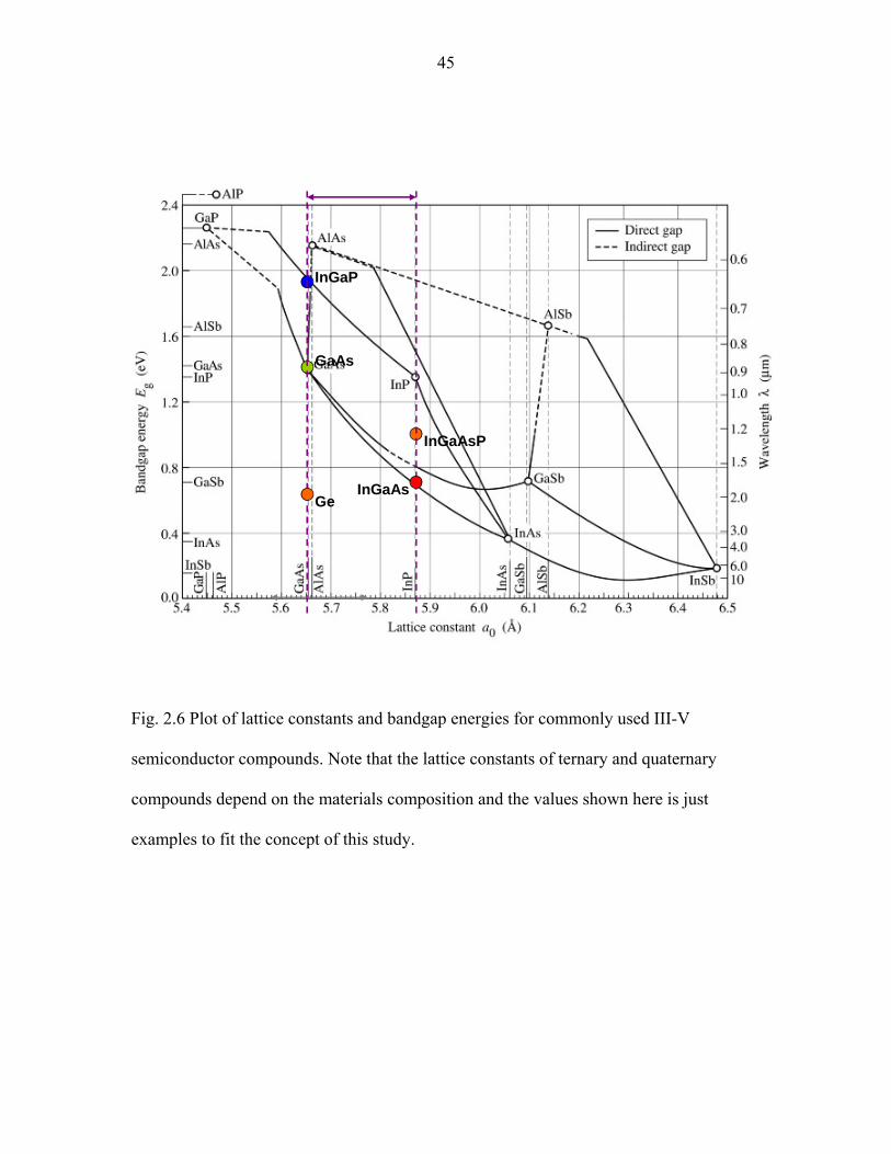
45
InGaAsP
InGaP
GeInGaAs
GaAs
InGaAsP
InGaP
GeInGaAs
GaAs
Fig. 2.6 Plot of lattice constants and bandgap energies for commonly used III-V
semiconductor compounds. Note that the lattice constants of ternary and quaternary
compounds depend on the materials composition and the values shown here is just
examples to fit the concept of this study.
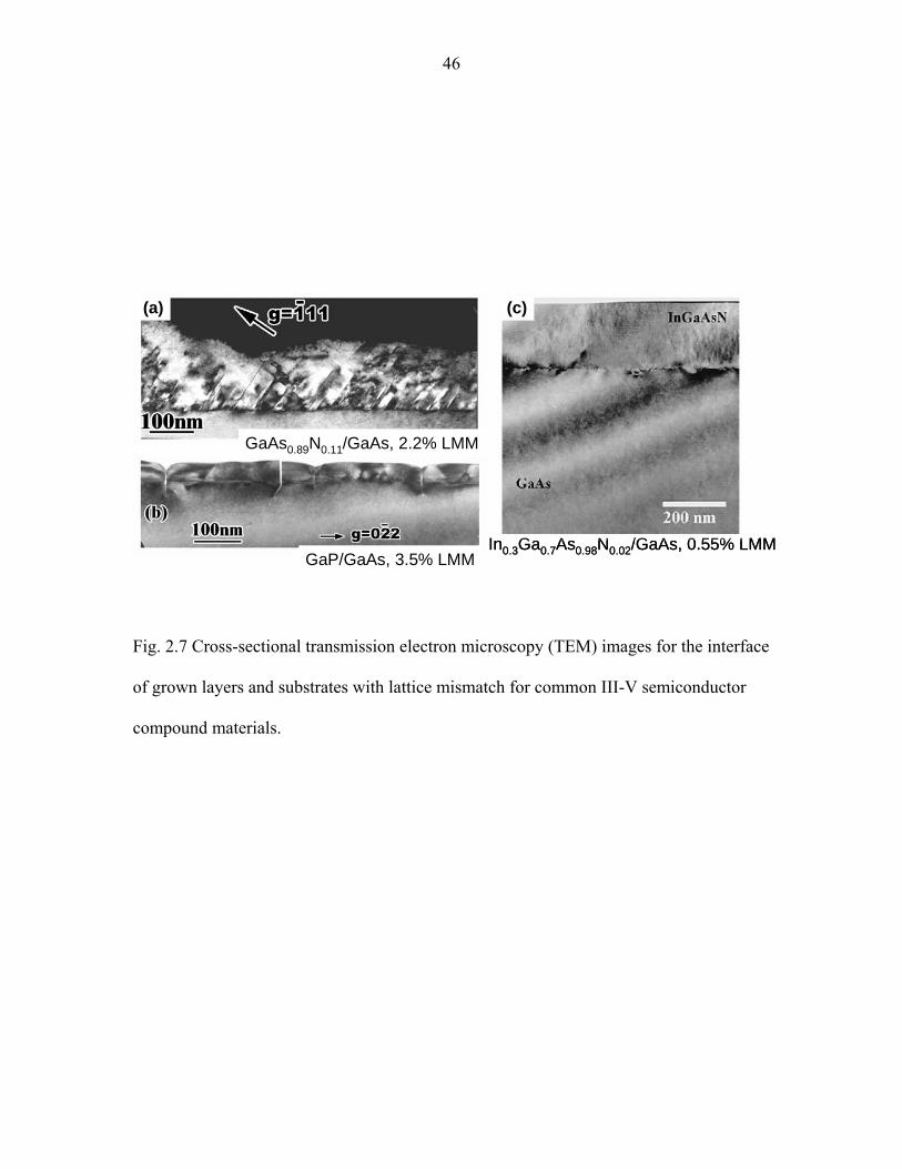
46
GaP/GaAs, 3.5% LMM
GaAs0.89N0.11/GaAs, 2.2% LMM
In0.3Ga0.7As0.98N0.02/GaAs, 0.55% LMM
(a) (c)
GaP/GaAs, 3.5% LMM
GaAs0.89N0.11/GaAs, 2.2% LMM
In0.3Ga0.7As0.98N0.02/GaAs, 0.55% LMM
(a) (c)
Fig. 2.7 Cross-sectional transmission electron microscopy (TEM) images for the interface
of grown layers and substrates with lattice mismatch for common III-V semiconductor
compound materials.
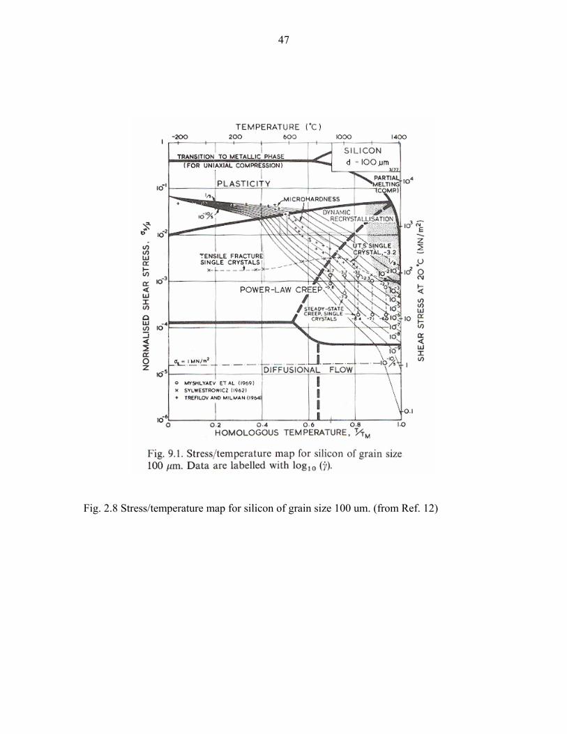
47
Fig. 2.8 Stress/temperature map for silicon of grain size 100 um. (from Ref. 12)
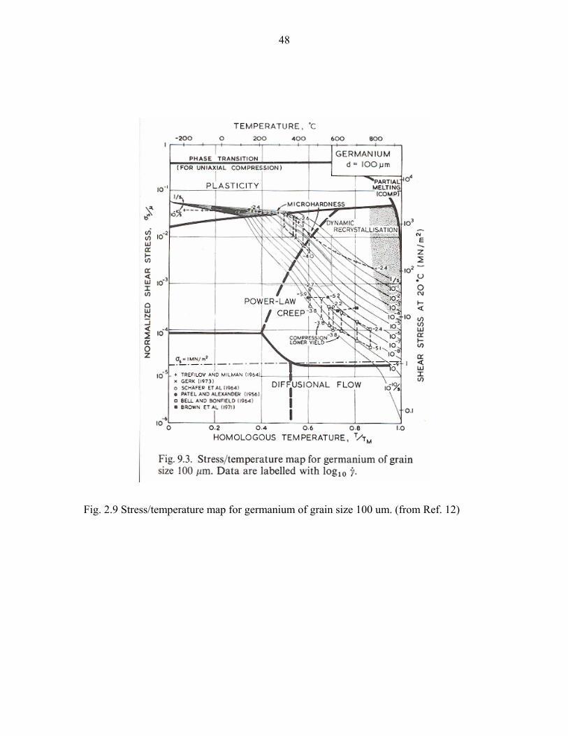
48
Fig. 2.9 Stress/temperature map for germanium of grain size 100 um. (from Ref. 12)

49
epi
epi
bondInGaAsP, 1.0eV
InGaAs, 0.7eV
GaAs, 1.4eV
Tunnel junction
Back contact
ContactCap ARAR
InGaP, 1.9eV
InP, substratea = 5.9Å
a = 5.6ÅTunnel junction
epi
epi
bondInGaAsP, 1.0eV
InGaAs, 0.7eV
GaAs, 1.4eV
Tunnel junction
Back contact
ContactCap ARAR
InGaP, 1.9eV
InP, substratea = 5.9Å
a = 5.6ÅTunnel junction
Fig. 2.10 Schematic cross section of the InGaP/GaAs/InGaAsP/InGaAs four-junction solar cell structure.

50
p SiInP SiInP
Cheaper!4” InP ~$1000/wafer4” Si ~$10/wafer
p SiInP SiInP
Cheaper!4” InP ~$1000/wafer4” Si ~$10/wafer
Fig. 2.11 Schematics of the cost reduction scheme by replacing conventional bulk InP
substrates with an alternative InP/Si substrate.
51
Chapter 3 GaAs/InP wafer bonding
3-1. Introduction
In the previous chapter, I explained why multijunction solar cells are efficient and
lattice-mismatched materials stacking would be good, how difficult to obtain high-quality
(i.e. low dislocation density) crystal layered structures of lattice-mismatched materials by
epitaxial growth, and the possibility of direct wafer bonding technique to overcome this
problem to give us the pathway to ultrahigh efficiency solar cells. In this chapter, I would
like to describe my investigation on direct wafer bonding of GaAs and InP applicable for
multijunction solar cell applications.
Aim of this study
For solar cell applications, the interfaces among semiconductor layers have to be highly
conductive not to reduce the cells’ energy conversion efficiency by dissipate the
transferred electronic carriers as heat due to the Ohmic loss. Therefore I investigated the
wafer bonding process of GaAs and InP to obtain Ohmic GaAs/InP junctions with low
resistance.
3-2. Experimental
Before studying the direct bonding of solar subcells, direct bonding of bulk GaAs
and InP wafers was investigated. (001) n-type GaAs and InP wafers doped respectively
with Si and S were used. The basic doping concentrations were 2x 1018 cm-3 Si in GaAs
and 4.5x 1018 cm-3 S in InP (both denoted as “n”). Interfacial bonding layers prepared by

52
MOCVD (metal-organic chemical vapor deposition) growth of thin epitaxial Se-doped
GaAs layers on GaAs with and S-doped InP on InP with doping concentration of 1x 10¹⁹
cm-3 (denoted as “n+”), schematically shown in Figure 3.1, were also investigated. These
n+ heavy doped bonding layers were 20 nm thick for GaAs and 500 nm thick for InP.
The GaAs and InP wafers were first coated with photoresist (Shipley 1813) with a
spincoater with a spinning velocity 3000 rpm for 1 min followed by soft bake at 115 oC
for 90 sec. This photoresist coating is to protect the bonding surfaces of GaAs and InP
from particles generate in the following dicing process because interfacial particles would
degrade the bonding strength. The wafers were then diced into ~1 cm2 area. Then the
applied photoresist was removed sequentially placed in boiling acetone with a beaker
placed on a hotplate at 115 oC for 10 min, in renewed acetone with a beaker placed in an
ultrasonic bath for 15 min, in methanol with a beaker placed in an ultrasonic bath for 15
min, and rinsed with D. I. (de-ionized) water. This series of washing process has also a
function of surface degreasing, as well as photoresist removal. Then the native oxide was
removed by dipping the GaAs and InP pieces in 7 vol%-HCl (aq) and 10 vol%-HF (aq),
respectively, for 30 sec. At this point, both of the GaAs and InP wafers are observed to be
highly hydrophobic. Then the wafers were brought into contact with their polished sides
face to face with the (011) edges aligned, as schematically shown in Figure 3.2. The
joined GaAs/InP pairs were annealed at ~0.5 MPa at 270 oC in atmosphere for 10 hours
followed by annealing in 10% H2 diluted by N2 (denoted as “H2/N2”) or N2 at 450-600 oC
for 30 min. Some bonded pairs were subject to only one of these two annealing
53
processes. A photograph of the wafer bonding facility used in this study is shown in
Figure 3.3.
The electrical properties of the bonded interfaces were investigated for the different
annealing conditions by measuring the current-voltage (I-V) characteristics. Bonded
pairs with both high and low doping concentrations at the subsequent bond interfaces
were investigated. Indium solder pads were used for Ohmic contact from the electrical
probes and the stage of the I-V measuring facility to the semiconductor materials, GaAs
and InP. Figure 3.4 shows a schematic of the materials configuration in the electrical
measurements for the bonded GaAs/InP wafers.
Secondary-ion mass spectroscopy (SIMS) depth profile measurements were
performed across the bonded interfaces of GaAs/InP to analyze the chemical composition
of the bonding interfaces. Cesium ions were used for sputtering to obtain depth profiles
of hydrogen and oxygen. This SIMS measurement was conducted by Bob (Robert)
Reedy at NREL (National Renewable Energy Laboratory).
3-3. Results and discussion
For multijunction solar cells, formation of mechanically robust, low resistance
interfaces is a critical aspect for structure stability and high energy conversion efficiency.
I-V characteristics were compared among the bonded nGaAs/nInP pairs with various
annealing conditions. Ohmic contact was obtained only for the pair annealed at 0.5 MPa

54
at 270 oC followed by annealing at 600 oC in H2/N2, as shown in Figure 3.5, which
indicates a significant effect of hydrogen at high temperature.
Figure 3.6 depicts the depth profiles of hydrogen and oxygen concentrations across
the bonded nGaAs/nInP heterointerfaces measured by SIMS before and after the
annealing in H2/N2 at 600 oC. This result shows a significant reduction of the interfacial
hydrogen and oxygen following the 600 oC anneal in H2/N2. The integrated dose of
oxygen after the 600 oC annealing corresponds to a layer with thickness of around 1 nm,
which is a reasonable value to induce tunneling current to enable one to obtain Ohmic
heterointerfaces, perhaps with some oxide breakdown by the applied voltage. [1, 2] A
general picture for the chemical evolution of the bonded bulk GaAs/InP interface could
be as follows: Upon room temperature bond initiation, the GaAs/InP interface is
characterized by mainly by van der Waals bonding. A covalently bonded GaAs/InP
interface is subsequently formed in annealing at 270 oC under pressure, mediated by a
thin interfacial oxide, as indicated by SIMS analysis. This is supported also by the fact
that the interface of the bonded pair has enough strength to endure the shear force applied
in the mechanical polishing process for the SIMS measurement. Applied pressure is
presumed to increase the interfacial contact area, as omission of an annealing step under
pressure resulted in non-Ohmic I-V characteristics. Higher-temperature annealing in
H2/N2 reduces hydrogen and oxygen at the bonded interface leading to higher interfacial
conductance.

55
Heavy doping at the GaAs and InP interfaces to be subsequently bonded was also
found to significantly enhance the GaAs/InP interfacial conductivity. Figure 3.7 shows
the I-V curves of the bonded GaAs/InP interfaces for the n+GaAs/n+InP pairs after
pressure annealing at 270 oC only and pressure annealing at 270 oC followed by
annealing in H2/N2 at 450 oC. This conductivity enhancement can be explained by
analysis of the heterojunction band offset at the GaAs/InP interface. Electron transport
rather than hole transport dominates the current flow in the n-type GaAs and InP used in
this study. (n.b., the conduction-band edge of GaAs is 0.3 eV above that of InP for
intrinsic materials. [3]) One-dimensional simulations of the heterojunction bandbending
indicate a significant decrease in the interface potential barrier width at higher doping
concentrations, especially on the GaAs side of a GaAs/InP heterojunction. [4] This
barrier thinning enables interfacial tunneling, rather than thermionic emission, leading to
higher conductivity across the heterojunction interfaces. [5, 6]
Ideally, Ohmic GaAs/InP heterojunctions would be formed by bonding at lower
temperature to avoid possible degradation of the cell interfaces and p-n junctions for
multijunction solar cell applications. The approach taken here yielded Ohmic interfaces
with < 0.10 Ohm-cm2 interface resistance at as low as 450 oC and < 1.0 Ohm-cm2 by
solely pressure annealing at 270 oC in n+GaAs/n+InP structures, as shown in Figure 3.5
3-4. Conclusions
In this section, low resistance Ohmic GaAs/InP junctions were obtained overcoming
~4% lattice mismatch using direct wafer bonding technique. The key factors were
56
reduction of the interfacial oxygen and hydrogen by annealing in reduction atmosphere
and high doping for the interfacial bonding layers to induce tunneling current. The
obtained bonded GaAs/InP structures are suitable for lattice-mismatched multijunction
solar cell applications with their highly conductive interfaces. Simple considerations
suggest that for such a cell the currently-reported interfacial resistance smaller than 0.1
Ohm-cm2 would result in a negligible decrease in overall cell efficiency of ~0.02%,
under 1-sun illumination. [7]
3-5. References
[1] E. Rosenbaum and L. F. Register, IEEE Trans. Electr. Dev. 44, 317, 1997.
[2] E. Miranda, J. Sune, R. Rodriguez, M. Nafria, and X. Aymerich, Appl. Phys. Lett. 73,
490, 1998.
[3] S. Tiwari and D. Frank, Appl. Phys. Lett. 60, 630-632, 1992.
[4] PC1D Version 5.2 (University of New South Wales), 1998.
[5] A. Y. C. Yu, Solid-St. Electron. 13, 239-247, 1970.
[6] H. Sasaki et al, Appl. Phys. Lett. 31, 211-213, 1977.
[7] P. R. Sharps, M. L. Timmons, J. S. Hills, and J. L. Gray, Proceedings of the 26th
IEEE Photovoltaic Specialists Conference (IEEE, New York, 1997), p. 895.

57
n wafer
n+ epi-layer(GaAs: 20nm,
InP: 500nm)n wafer
n+ epi-layer(GaAs: 20nm,
InP: 500nm)
Fig. 3.1 Cross-sectional schematic of the III-V semiconductor compound wafer with a
heavy doped bonding layer.

58
1cm
0.5cmInP
GaAs
[001]
[110]
1cm
0.5cmInP
GaAs
[001]
[110]
Fig. 3.2 Typical configuration of the bonded pair of semiconductor compound wafers.

59
Fig. 3.3 Photograph of the wafer bonder used in this study.
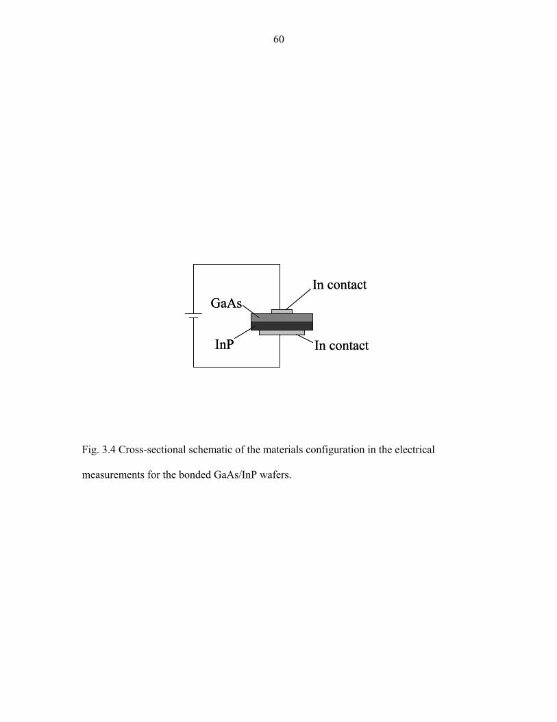
60
In contact
In contact
GaAs
InP
In contact
In contact
GaAs
InP
Fig. 3.4 Cross-sectional schematic of the materials configuration in the electrical
measurements for the bonded GaAs/InP wafers.
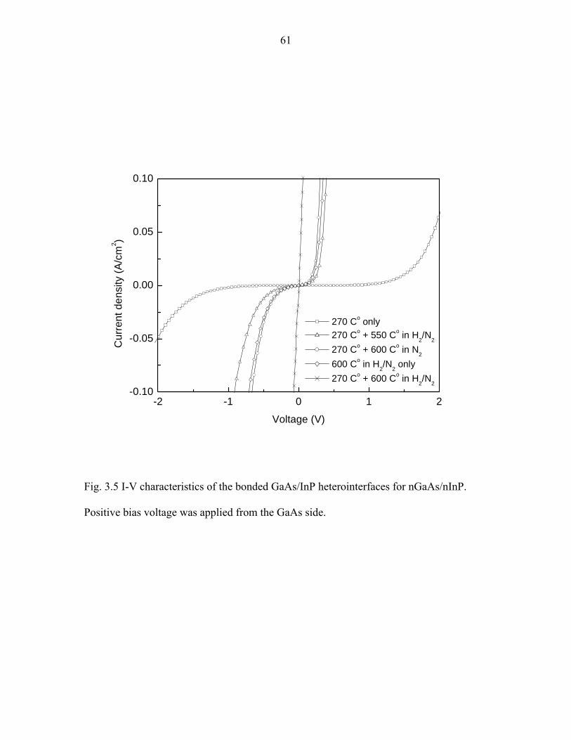
61
-2 -1 0 1 2-0.10
-0.05
0.00
0.05
0.10
Cur
rent
den
sity
(A/c
m2 )
Voltage (V)
270 Co only 270 Co + 550 Co in H
2/N
2
270 Co + 600 Co in N2
600 Co in H2/N2 only 270 Co + 600 Co in H
2/N
2
Fig. 3.5 I-V characteristics of the bonded GaAs/InP heterointerfaces for nGaAs/nInP.
Positive bias voltage was applied from the GaAs side.
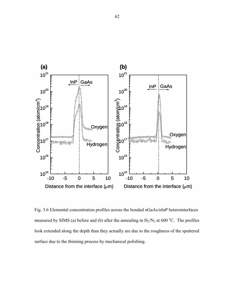
62
Fig. 3.6 Elemental concentration profiles across the bonded nGaAs/nInP heterointerfaces
measured by SIMS (a) before and (b) after the annealing in H2/N2 at 600 oC. The profiles
look extended along the depth than they actually are due to the roughness of the sputtered
surface due to the thinning process by mechanical polishing.
-10 -5 0 5 101015
1016
1017
1018
1019
1020
1021
Hydrogen
Oxygen
(a)
InP GaAs
Con
cent
ratio
n (a
tom
/cm
3 )
Distance from the interface (μm)
-10 -5 0 5 101015
1016
1017
1018
1019
1020
1021
Hydrogen
Oxygen
(b)
GaAsInP
Con
cent
ratio
n (a
tom
/cm
3 )
Distance from the interface (μm)
-10 -5 0 5 101015
1016
1017
1018
1019
1020
1021
Hydrogen
Oxygen
(a)
InP GaAs
Con
cent
ratio
n (a
tom
/cm
3 )
Distance from the interface (μm)
-10 -5 0 5 101015
1016
1017
1018
1019
1020
1021
Hydrogen
Oxygen
(b)
GaAsInP
Con
cent
ratio
n (a
tom
/cm
3 )
Distance from the interface (μm)

63
-1.0 -0.5 0.0 0.5 1.0-0.3
-0.2
-0.1
0.0
0.1
0.2
0.3
Cur
rent
den
sity
(A/c
m2 )
Voltage (V)
270 Co only 270 Co + 450 Co in H2/N2
Fig. 3.7 I-V characteristics of the bonded GaAs/InP heterointerfaces for n+GaAs/n+InP.
Positive bias voltage was applied from the GaAs side.
64
Chapter 4 Direct-bonded dual-junction GaAs/InGaAs
solar cells
4-1. Introduction
In the previous chapter, low resistance, Ohmic GaAs/InP junctions were successfully
fabricated via direct wafer bonding. In this chapter, the obtained GaAs/InP wafer bonding
technique is actually applied for lattice-mismatched multijunction solar cell fabrication.
GaAs subcells lattice matched to and grown on GaAs substrates and In0.53Ga0.47As
subcells lattice matched to and grown on InP substrates are bonded to form GaAs/
In0.53Ga0.47As lattice-mismatched dual-junction solar cells.
Aim of this study
This chapter shows the very first demonstration of multijunction solar cell fabrication
via direct wafer bonding. The characterization results for the fabricated solar cells are
also presented.
4-2. Experimental
In the second phase of this study for GaAs/InP direct wafer bonding following Chapter
3, a two-terminal monolithic, dual-junction tandem solar cell was fabricated from direct
bonding of single-junction GaAs and InGaAs subcells. The GaAs and InGaAs subcells
were prepared by Daniel Aiken at Emcore Photovoltaics and Mark Wanlass at NREL
(National Renewable Energy Laboratory), respectively. Figures 4.1 (a) and (b) show
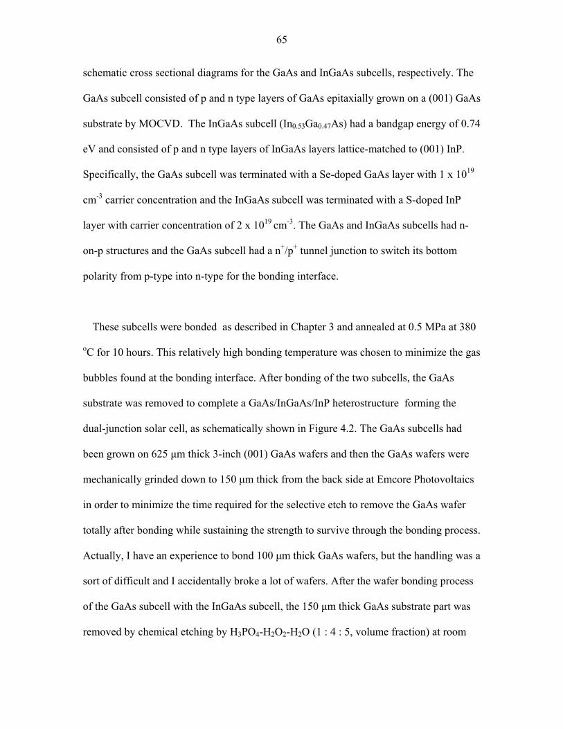
65
schematic cross sectional diagrams for the GaAs and InGaAs subcells, respectively. The
GaAs subcell consisted of p and n type layers of GaAs epitaxially grown on a (001) GaAs
substrate by MOCVD. The InGaAs subcell (In0.53Ga0.47As) had a bandgap energy of 0.74
eV and consisted of p and n type layers of InGaAs layers lattice-matched to (001) InP.
Specifically, the GaAs subcell was terminated with a Se-doped GaAs layer with 1 x 10¹⁹
cm-3 carrier concentration and the InGaAs subcell was terminated with a S-doped InP
layer with carrier concentration of 2 x 1019 cm-3. The GaAs and InGaAs subcells had n-
on-p structures and the GaAs subcell had a n+/p+ tunnel junction to switch its bottom
polarity from p-type into n-type for the bonding interface.
These subcells were bonded as described in Chapter 3 and annealed at 0.5 MPa at 380
oC for 10 hours. This relatively high bonding temperature was chosen to minimize the gas
bubbles found at the bonding interface. After bonding of the two subcells, the GaAs
substrate was removed to complete a GaAs/InGaAs/InP heterostructure forming the
dual-junction solar cell, as schematically shown in Figure 4.2. The GaAs subcells had
been grown on 625 μm thick 3-inch (001) GaAs wafers and then the GaAs wafers were
mechanically grinded down to 150 μm thick from the back side at Emcore Photovoltaics
in order to minimize the time required for the selective etch to remove the GaAs wafer
totally after bonding while sustaining the strength to survive through the bonding process.
Actually, I have an experience to bond 100 μm thick GaAs wafers, but the handling was a
sort of difficult and I accidentally broke a lot of wafers. After the wafer bonding process
of the GaAs subcell with the InGaAs subcell, the 150 μm thick GaAs substrate part was
removed by chemical etching by H3PO4-H2O2-H2O (1 : 4 : 5, volume fraction) at room

66
temperature around for 1 hour. Regular commercial 85% H3PO4 and 30% H2O2 chemical
bottles and 18 Mega Ohm de-ionized (D. I.) water were used. I dipped the bonded
GaAs/InGaAs structure in the chemical solution until I saw the shiny smooth surface of
the InGaP etch-stop layer. The etching solution was regularly agitated for two purposes:
one is to prevent spatial migration of the chemicals, which would significantly decelerate
the etching reaction, due to the large H3PO4 weight and the other is to keep the areal
uniformity of etching rate.
Then I deposited metal top and bottom contacts to the bonded dual-junction solar cell
structures by thermal evaporation of Au. 150 nm thick Au was deposited by thermal
evaporation with a deposition rate of ~5 Å/s on both of the cell front and back sides. No
photolithography process was used, but a simply physical mask was applied for the
evaporation to form a square ring-type front contacts. It should be noted that I missed to
remove the 50 nm thick GaAs contact layer, which is supposed to exist only underneath
of the front metal contact, simply due to my lack of knowledge and experience at the
moment of this project. Proper removal of this contact layer would have increased the
solar cell photocurrent and efficiency by minimize the wasted light absorption in the
contact layer. Such front contact layers were properly removed for the projects of InGaAs
solar cells on InP/Si substrates (Chapter 6) and plasmonic GaAs solar cells (Chapter 7).
The cells were then annealed in H2/N2 at 350 oC for 30 min to form Ohmic metal contacts.
It should be noted that the process conditions for the metallization and annealing were not
optimized mainly because the number of the GaAs and InGaAs subcell samples delivered
from Emcore and NREL was limited. Through the plasmonic GaAs project, to be
described in Chapter 7, I have got a feeling that this annealing temperature of 350 oC may
67
have been too high and probably caused some electrical shunting at the p-n junctions due
to Au diffusion to reduce the open-circuit voltage of the cell.
Photovoltaic I-V characteristics of the bonded GaAs/InGaAs dual-junction cell were
measured with 0.337 cm2 active illumination area under AM1.5 Global solar spectrum
with 1-sun total intensity (100 mW cm-2). For comparison, photovoltaic I-V
characteristics of the unbonded GaAs and InGaAs subcells were also measured. Each of
the subcells was processed in the same way as the bonded GaAs/InGaAs cell. The GaAs
subcell was mounted on a handling glass substrate with gold film via conductive silver-
epoxy glue, for its inversely-grown structure, and the original GaAs substrate was
removed by the same chemical etching used for the bonded dual-junction cells. A cross-
sectional schematic of this reference GaAs cell is shown in Figure 4.3. Regular plain
smooth glass micro slides such as Corning 2947 with a thickness of ~1 mm were diced
into ~ 1cm X 1cm size and 150 nm thick Au was deposited by thermal evaporation with a
deposition rate of ~5 Å/s on the glass slides. The silver-epoxy glue was roughly a 1:1
(volume ratio) mixture of Epoxy Technology H20E-175 Part A and Part B, which bonded
the inversely grown GaAs cells and the Au-deposited glass plates by being cured on a
180 oC hotplate for 2 hours in the atmosphere.
4-3. Results and discussion
Figures 4.4 and 4.5 show AFM images of the bonding surface of the GaAs top subcell
and the InGaAs bottom subcell. The measured root-mean-square (RMS) roughness for
each subcell was around 10 Å or a little less than that for both of the GaAs subcell and

68
the InGaAs subcell. This surface roughness was smooth enough to give successful direct
wafer bonding, while other test cell samples with RMS roughness around 100 Å were not
successfully bonded with similar process conditions. Additionally, the RMS roughness
for the GaAs and InP commercial epi-ready wafers used for the wafer bonding study in
Chapter 3 was 3-5 Å.
The photovoltaic I-V characteristics of the bonded GaAs/InGaAs dual-junction solar
cell are shown in Figure 4.6 (inset). The device parameters for this cell were Jsc = 12.5
mA cm-2, Voc = 1.20 V, FF = 0.62, and η = 9.3 %, where Jsc, Voc, FF and η are short-
circuit current, open-circuit voltage, fill factor and energy conversion efficiency,
respectively. The low fill factor may be accounted for by series resistance in the contacts,
which can be lowered by contact redesign. The interfacial resistance for bulk GaAs/InP
bonded under the conditions used for the cell was only around 10% of the total series
resistance of the cell estimated from the photovoltaic I-V characteristics. The Vocs of the
unbonded GaAs and InGaAs subcells were 0.91 V and 0.27 V. Thus, the Voc of the
bonded GaAs/InGaAs dual-junction cell was approximately equal to the sum of the open
circuit voltages for the GaAs and InGaAs subcells. This Voc result indicates that the
bonding process does not degrade the cell material quality since any generated crystal
defects that act as recombination centers would reduce Voc. [1, 2] Also, the bonded
interface has no significant carrier recombination rate to reduce the open circuit voltage.
The spectral response for the bonded dual-junction cell and unbonded GaAs and InGaAs
subcells is given in Figure 4.6. The bottom InGaAs subcell as well as the top GaAs
69
subcell of the bonded tandem cell was found to be photovoltaically active. This result
indicates a highly transparent bonded GaAs/InGaAs interface. The result of the bonded
cell is similar to the unbonded subcells in spectral response and indicates only a small
loss of quantum efficiency (~10 %) by the cell stacking with direct wafer bonding. The
poor quantum efficiency, specifically for the higher energy region, may be caused by a
high surface recombination rate at the top surface. [3] Anti-reflective coating, surface
passivation and optimization of cell assembly parameters, such as metal contacts and
current matching, would give further improvement of the cell efficiency.
4-4. Conclusions
In this chapter, we demonstrated use of direct wafer bonding in a tandem solar cell for
the first time. Such an approach can also be applied to other photovoltaic heterojunctions
where lattice mismatch accommodation is also a challenge, such as the
InGaP/GaAs/InGaAsP/InGaAs four-junction tandem cell, schematically shown in Figure
4.7, by bonding a GaAs-based lattice-matched InGaP/GaAs subcell to an InP-based
lattice-matched InGaAsP/InGaAs subcell.
4-5. References
[1] R. B. Bergmann, Appl. Phys. A 69, 187, 1999.
[2] R. Brendel, Jpn. J. Appl. Phys. 40, 4431, 2001.
[3] K. A. Bertness, S. R. Kurtz, D. J. Friedman, A. E. Kibbler, C. Kramer, and J. M.
Olson, Appl. Phys. Lett. 65, 989, 1994.

70
150um GaAs substrate (semi insulating)
100nm GaAs buffer (non doped)100nm InGaP etch stop (non doped)50nm GaAs contact layer (Si doped)
35nm InGaP window (Si doped)150nm GaAs emitter (Si doped 1x1018cm-3)
33nm GaAs intrinsic layer (non doped)3um GaAs base (Zn doped 2x1017cm-3)
25nm AlGaAs BSF (C doped)35nm AlGaAs p++ tunnel junction (Si doped)25nm AlGaAs n++ tunnel junction (Se doped)
Removedafter bond
Bondingsurface
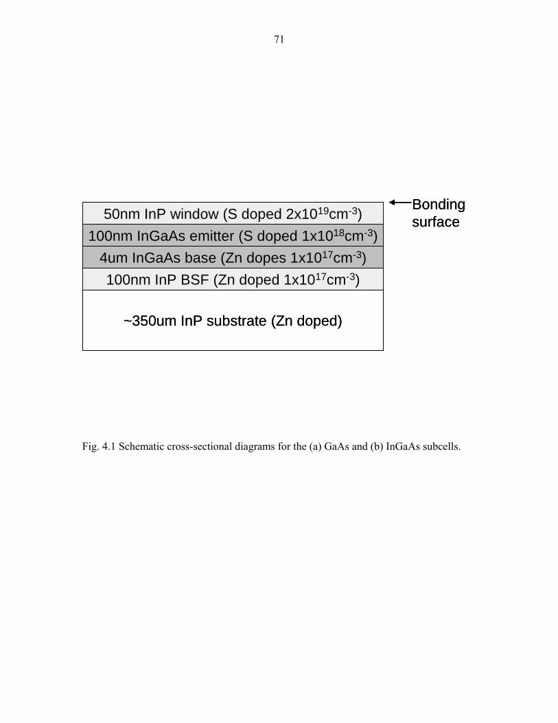
71
~350um InP substrate (Zn doped)
100nm InP BSF (Zn doped 1x1017cm-3)4um InGaAs base (Zn dopes 1x1017cm-3)
100nm InGaAs emitter (S doped 1x1018cm-3)50nm InP window (S doped 2x1019cm-3)
Bondingsurface
~350um InP substrate (Zn doped)
100nm InP BSF (Zn doped 1x1017cm-3)4um InGaAs base (Zn dopes 1x1017cm-3)
100nm InGaAs emitter (S doped 1x1018cm-3)50nm InP window (S doped 2x1019cm-3)
Bondingsurface
Fig. 4.1 Schematic cross-sectional diagrams for the (a) GaAs and (b) InGaAs subcells.
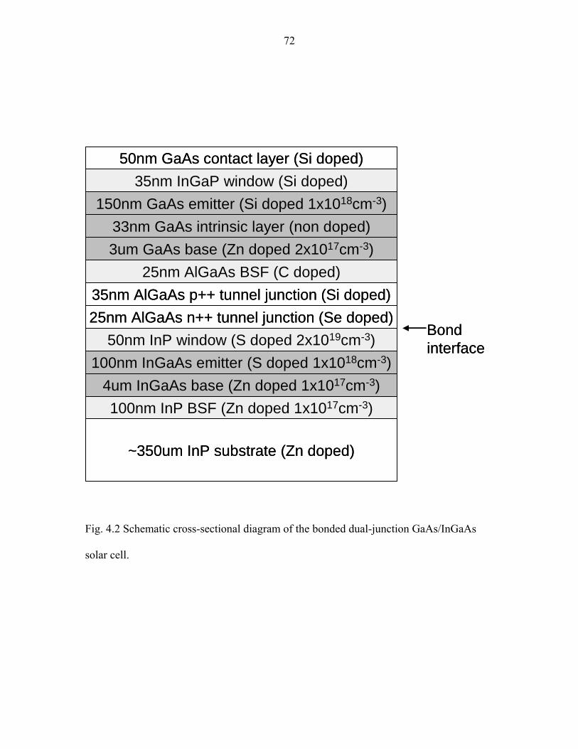
72
~350um InP substrate (Zn doped)
100nm InP BSF (Zn doped 1x1017cm-3)4um InGaAs base (Zn doped 1x1017cm-3)
100nm InGaAs emitter (S doped 1x1018cm-3)50nm InP window (S doped 2x1019cm-3)
Bondinterface
50nm GaAs contact layer (Si doped)35nm InGaP window (Si doped)
150nm GaAs emitter (Si doped 1x1018cm-3)33nm GaAs intrinsic layer (non doped)3um GaAs base (Zn doped 2x1017cm-3)
25nm AlGaAs BSF (C doped)35nm AlGaAs p++ tunnel junction (Si doped)25nm AlGaAs n++ tunnel junction (Se doped)
Fig. 4.2 Schematic cross-sectional diagram of the bonded dual-junction GaAs/InGaAs
solar cell.
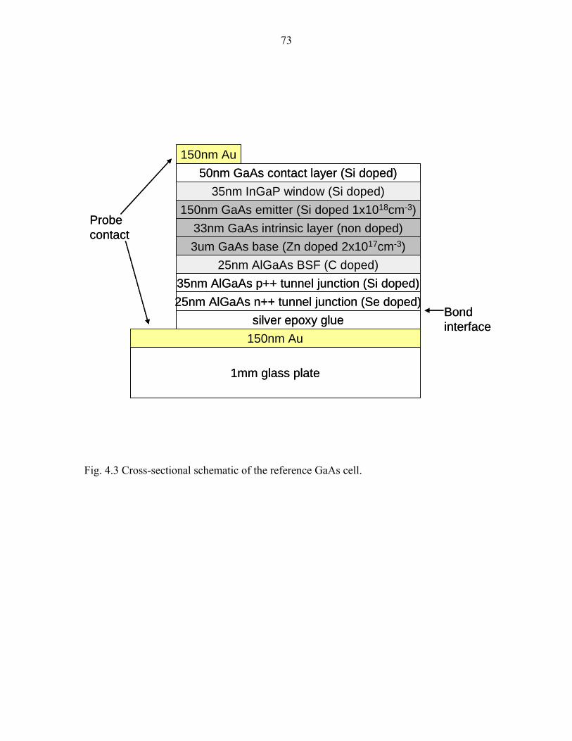
73
Bondinterface
50nm GaAs contact layer (Si doped)35nm InGaP window (Si doped)
150nm GaAs emitter (Si doped 1x1018cm-3)33nm GaAs intrinsic layer (non doped)3um GaAs base (Zn doped 2x1017cm-3)
25nm AlGaAs BSF (C doped)35nm AlGaAs p++ tunnel junction (Si doped)25nm AlGaAs n++ tunnel junction (Se doped)
silver epoxy glue150nm Au
1mm glass plate
150nm Au
Probecontact
Fig. 4.3 Cross-sectional schematic of the reference GaAs cell.

74
Fig. 4.4 AFM topological images of the bonding surface for the GaAs top subcell. The
RMS roughness was around 10 A. Note that the abrupt horizontal lines are due to
instrumental artificial noise and should be neglected.

75
Fig. 4.5 AFM topological images of the bonding surface for the InGaAs bottom subcell.
The RMS roughness was around 10 A. Note that the abrupt horizontal lines are due to
instrumental artificial noise and should be neglected.
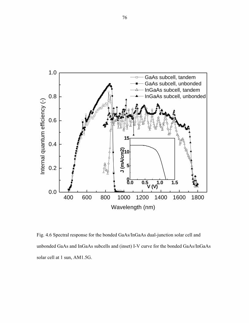
76
400 600 800 1000 1200 1400 1600 18000.0
0.2
0.4
0.6
0.8
1.0
0.0 0.5 1.0 1.50
5
10
15
J (m
A/cm
2)
V (V)
In
GaAs subcell, tandem GaAs subcell, unbonded
InGaAs subcell, tandem InGaAs subcell, unbonded
(-)
Fig. 4.6 Spectral response for the bonded GaAs/InGaAs dual-junction solar cell and
unbonded GaAs and InGaAs subcells and (inset) I-V curve for the bonded GaAs/InGaAs
solar cell at 1 sun, AM1.5G.
tern
qutu
ee
y
Wavelength (nm)
ncffi
cim
anal

77
InGaAsP, 1.0eV
InGaAs, 0.7eV
GaAs, 1.4eV
Tunnel junction
Back contact
ContactCap ARAR
InGaP, 1.9eV
InP, substratea = 5.9Å
a = 5.6ÅTunnel junction
bondInGaAsP, 1.0eV
InGaAs, 0.7eV
GaAs, 1.4eV
Tunnel junction
Back contact
ContactCap ARAR
InGaP, 1.9eV
InP, substratea = 5.9Å
a = 5.6ÅTunnel junction
bond
Fig. 4.7 Schematic cross-sectional diagram of an ultrahigh efficiency
InGaP/GaAs/InGaAsP/InGaAs four-junction solar cell.

78
Chapter 5 InP/Si bonding and InP layer transfer
5-1. Introduction
In the previous chapters, I explained that multijunction solar cells of III-V
semiconductor compounds exhibit very high energy conversion efficiencies. However,
production cost is an important key factor as well as energy conversion efficiency for
wide use of such solar cells specifically for terrestrial use. Let us take a look at the
schematic diagram of the four-junction solar cell again in Figure 5.1. Simply looking at
the thickness of each layer, we notice that the InP substrate dominates the most fraction
of the total thickness of the cell with it’s thickness of a couple of hundreds micron
relative to the other layers of a couple of micron thick at most. Therefore we would like
to reduce the cost of the InP substrate, which has a large fraction of the fabrication cost
for the solar cell.
Engineered substrates consisting of thin films of InP on Si handle substrates (InP/Si
substrates or epitaxial templates) have the potential to significantly reduce the cost and
weight of compound semiconductor solar cells relative to those fabricated on bulk InP
substrates. InGaAs solar cells on InP have superior performance to Ge cells at photon
energies greater than 0.7 eV. The current record efficiency cell for 1 sun illumination was
achieved using an InGaP/GaAs/InGaAs triple junction cell design with an InGaAs
bottom cell [1]. Thermophotovoltaic (TPV) cells from the InGaAsP-family of III-V
materials grown epitaxially on InP substrates would also benefit from such an InP/Si
substrate [2]. Substitution of InP/Si substrates for bulk InP in the fabrication of such a

79
four-junction solar cell could significantly reduce the substrate cost. For example, typical
price of a 4-inch InP wafer is ~$1000/wafer, relative to ~$10/wafer for a 4-inch Si wafer,
as of Aug. 2007. Switching the major part of growth substrates from InP or other III-V
materials into Si also has such advantages as follows. Si is mechanically more robust than
III-V semiconductor compound materials. Si has higher thermal conductivity than III-V
materials do and therefore would have less energy conversion efficiency loss due to
increased temperature of solar cells specifically for optical concentrator use. Si has
lighter (~1/2) weight than III-V materials do, which would particularly be a benefit for
space use.
Direct heteroepitaxial growth of InP thin films on Si substrates has not produced the low
dislocation-density high quality layers required for active InGaAs/InP in optoelectronic
devices due to the ~8% lattice mismatch between InP and Si [3]. Wafer bonding on the
other hand is not subject to lattice matching limitations associated with epitaxial growth,
and has been used to fabricate materials that consist of crystalline semiconductors on
amorphous materials and also to integrate crystalline materials of different lattice
constants. For the integration of both crystalline-amorphous and crystalline-crystalline
pairs, defects caused by the lack of crystallographic registry are isolated to the wafer-
bonded interface. Thus, provided the wafer-bonded interface does not play an active role
in the operation of the device, the independent materials and devices fabricated in them
can in principle have performance typical of devices made on or in the bulk material.

80
Layer transfer of a high quality single crystal InP film onto a Si bulk substrate can be
accomplished through wafer bonding of InP to Si and exfoliation of a thin film from the
InP wafer induced by implantation of light elements such as hydrogen and helium [4-6].
The implantation process results in a high density of point defects near the region where
exfoliation occurs, however most of this region can be removed by thinning the
transferred film. Furthermore, the point defects generated by the implantation process
have previously been shown to have minimal impact on the quality of InP grown on
transferred thin films of InP [7]. This is likely because during the epitaxial process,
vacancies in the growth surface are occupied by the appropriate anion or cation adatom.
Because only a few μm of InP are consumed in the transfer of a film and subsequent
reclaim of the InP substrate, a single InP wafer could be reused repeatedly to generate
many InP/Si substrates, thus reducing the material cost of InP in devices grown on those
substrates.
Overview of this study
First I fabricated InP/Si direct-bonded, layer-transferred epitaxial substrates, but
delamination in the MOCVD growth process is observed. Aonex Technologies, Inc., one
of my collaborators and whom I have been sharing technical information with each other
throughout this project, successfully made InP/SiO2/Si substrates and were good in the
growth of InGaAs solar cells. For the detail of the InGaAs solar cell growth on the
prepared InP/SiO2/Si substrates and cells’ characterization will be described in the
following chapter.
81
5-2. InP/Si direct-bonded alternative substrate
5-2-1. Experimental
Ion-implantation-induced exfoliation of InP
The basic process schematic for the InP layer transfer to fabricate alternative InP/Si
epitaxial substrate (epitaxial templates) is shown in Figure 5.2. Epi-ready p-type (Zn
doped) 2-inch InP (100) wafers with doping concentration of 4x1018 cm-3 were purchased
from InPACT, Inc. He+ and H+ ions were implanted into the doses of 1x1017 cm-2 and
1.5x1016 cm-2, respectively, with implantation energies and currents of 115 keV, 80 μA
and 80 keV, 150 μA, respectively. The implantation was done into the polished side of
the InP wafers. The ion implantation was done by Leonard J. Kroko, Inc. These
implantation doses and currents were carefully chosen through trial and error based on
the two points:
1. The implantation dose has to be large enough to exfoliate the InP wafers in the
following bonding/annealing process
2. The implantation current has to be low enough to avoid partial exfoliation of the InP
wafers due to the accumulated heat by implantation energy flux
Therefore, ideally it would be better to have higher implantation dose and lower
implantation current. However the process time, which is proportional to implantation
dose divided by implantation current, reflects the implantation cost and therefore those
two parameters had to be optimized. The implantation energies or voltages determines
the implantation depth and were chosen to give ~1 um implantation depth for both of He+
and H+ using SRIM, a Monte-Carlo simulation package for implantation depth profiles.
For this study, p-type InP wafers were mainly used since III-V semiconductor compound

82
solar cells are typically grown to n-type photovoltaic active layers at the top and p-type
layers at the bottom. It should be however noted that I succeeded in layer transfer also of
n-type (S doped) InP with the same process conditions. I have not investigated deeply,
but helium-only implantation may also work, as seen in the InP/SiO2/Si substrate
fabrication by Aonex Technologies, Inc. described in the following section.
Wafer bonding and layer transfer
p-type conductive (doping concentration > 1x1018 cm-3) Si (001) epi-ready wafers were
used as the supporting substrate. After implantation, the InP wafers were first coated with
photoresist (Shipley 1813) with a spincoater with a spinning velocity 3000 rpm for 1 min
followed by soft bake at 115 oC for 90 sec. This photoresist coating is to protect the
bonding surface of InP from particles generate in the following dicing process because
interfacial particles would degrade the bonding strength. The wafers were then diced into
quarters of the original 2 inch diameter size. Then the applied photoresist was removed
sequentially dipped in acetone for 10 min and then in methanol for 10 min, and rinsed
with D. I. (de-ionized) water. This series of washing process has also a function of
surface degreasing, as well as photoresist removal. Then the native oxide was removed
by dipping both the InP and Si wafers in 10 vol%-HF (aq) for 30 sec. At this point, both
of the GaAs and InP wafers are observed to be highly hydrophobic. Surface activation by
oxygen plasma was also tested, but this surface treatment prior to wafer bonding oxidized
the wafers and made the two wafer surfaces to be bonded repulsive like same polarity of
magnets and therefore was not adopted in this study. Then the wafers were brought into
contact with their polished sides face to face with the (011) edges aligned. The joined

83
InP/Si pair was annealed at ~1 MPa at 400 oC in atmosphere for 10 hours to make InP/Si
bond and also to exfoliate an InP thin film by thermal expansion of the implanted ions.
The wafer bonding facility used in this study was same as the one used in Chapters 3 and
4 and its photograph is shown in Figure 3.1 in Chapter 3. As the result of this process, a
structure of a ~900 nm thick InP thin film bonded on top of a Si substrate is obtained, as
its photograph is shown in Figure 5.3. Because of the quite thin thickness of the
exfoliated InP film, in principle we could fabricate hundreds of the alternative InP/Si
epitaxial substrates from a single InP wafer, which has potential of a significant
production cost reduction of III-V semiconductor compound solar cells.
Smoothening of InP surface
The as-transferred InP/Si alternative substrates have rough InP surface inappropriate
for subsequent epitaxial growth. Also, due to the implantation-induced damage around at
the exfoliation surface in InP wafers, removal of such damage region is needed for proper
subsequent epitaxial growth. [5, 8] I therefore attempted to remove the damage region as
well as smoothening the InP surface by using chemical etching and also by chemical
mechanical polishing (CMP). Chemical etching was carried out using combinations of
oxidizers such as H2O2, dissolving strong acids such as HCl and diluents such as H3PO4
at room temperature. CMP process was carried out using a PM5 polisher (Logitec, Inc.)
with a soft polyurethane polishing pad (“Politex” cloth, Eminess Technologies, Inc.)
rotated at ~10 rpm using (chemicals) with an applied pressure of ~50 kPa in the
Nanofabrication Laboratory in UCLA. The InP/Si substrates were mounted on either a 4-
inch glass plate or silicon wafer via crystal bond and then attached to a wafer jig. A

84
chemical solution consisting of 1:10 (vol.) sodium hypochlorite (NaOCl) (5-6% aq.) -
H2O and 1:2 (vol.) citric acid (C6H8O7) (10% aq.) -H2O was regularly applied to the
polishing pad to assist polishing. [9] No abrasive particle was used.
Contact-mode atomic force microscopy (AFM) measurement was used to determine
the surface roughness for the as-transferred and smoothened InP surface of the InP/Si
alternative substrates.
InGaAs growth on the InP/Si alternative substrates
To test the quality of the fabricated InP/Si alternative substrate as an epitaxial growth
substrate relative to bulk InP substrates, lattice-matched InP/In0.53Ga0.47As/InP double
heterostructures (DHs) were grown with metalorganic chemical vapor deposition
(MOCVD). This MOCVD growth was done by Daniel Law at Spectrolab, Inc. The DHs
were grown simultaneously on the layer-transferred (100) InP / (100) Si structures and
also on a bulk (100) InP control wafer. The InP/InGaAs/InP DH was capped by an
InGaAs layer.
5-2-2. Results and discussion
Smoothening of InP surface
Figure 5.4 shows a typical AFM topological image for InP surface of the as-transferred
InP/Si alternative substrate. The measured root-mean-square (RMS) roughness was
around 100 Å, which is much larger than the typical value for epi-ready substrates, 1-10
Å. Therefore I tried to smoothen this rough surface for subsequent epitaxial growth by
85
using liquid-phase chemical etching and chemical mechanical polishing (CMP)
techniques.
Chemical etching solutions for III-V and IV group semiconductors such as GaAs, InP,
Si and Ge commonly consist of oxidizers to first form semiconductor oxide solvable with
acids, acids to dissolve the semiconductor oxide and diluents, typically weak acids, to
adjust the etching rate and surface roughness. For the case of InP etching and
smoothening, first InPO4 or In2O3 is formed at the surface of InP by an oxidizer such as
H2O2 and then this oxide is dissolved by a strong acid such as HCl, as schematically
depicted in Figure 5.5. [10, 11]
Table 5.1 shows the list of the chemical solutions used in this study for InP smoothening.
Out of this list, only HCl-H2O2-H3PO4 [11-14] and HCl-H2O2-CH3COOH [15-17] were
found to exhibit notable smoothening effect. AFM images for the morphological
evolution of the InP surface by the HCl-H2O2-H3PO4 etching is shown in Figure 5.6. The
finished RMS roughness of the InP surface was ~30 Å for both 1:2:2 (volume fraction)
solution at the point of 1 min dip and 1:7:2 solution at 1 min or later. The etching rate
was determined to be 360 nm/min and 35 nm/min for 1:2:2 and 1:7:2 solutions,
respectively. 1:7:2 HCl-H2O2-CH3COOH solution (40 nm/min) also resulted in ~30 Å
RMS roughness at 4 min, while no smoothening was observed for 1:2:2 HCl-H2O2-
CH3COOH (1300 nm/min). Dilution of the acid (dissolver) seemingly gives more or less
smoother etching. This result can be attributed to mass-transfer-limited chemical reaction,
where etch rates at peaks are higher than etch rates at valleys and hence the surface is

86
smoothened. Larger oxidizer fraction relative to acid may also have higher smoothening
effect due to dissolution-limited circumstance since oxidation process is more sensitive to
electron concentration, surface orientation, crystal defects and so forth, which would
cause higher areal nonuniformity for etching rate. [18, 19]
As described above, proper chemical etching could successfully smoothen the InP
surface of the InP/Si alternative substrate down to RMS roughness ~30 Å relative to ~100
Å as layer-transferred. However, this roughness is still not quite ideal for subsequent
epitaxial growth compared with 1-10 Å RMS roughness for commercial
”epi-ready” bulk substrates. Therefore, I also tried chemical mechanical polishing (CMP),
which is commonly used in semiconductor industry for epi-ready surface preparation.
Figure 5.7 shows AFM topological images for some of the successful resulted InP surface
of the InP/Si substrates. RMS roughness as small as 3 Å at best has been achieved. Etch
pits were occasionally found presumably stemming from intrinsic etch pits existing in the
InP wafers selectively etched in CMP. This obtained RMS roughness is quite comparable
to the commercially-available “epi-ready” grade semiconductor substrates, which means
appropriate for epitaxial growth. It should be however noted that CMP process has
somehow poor reproducibility for resulted surface. The polishing rate and areal
uniformity are very sensitive to the condition and only a slight difference of the process
condition we would not notice could give a drastic difference to the result. Therefore it is
crucial to choose stable conditions for CMP operation through trials.
Growth of InP/InGaAs double heterostructures
87
Figure 5.8 (a) and (b) show typical cross-sectional scanning electron microscopy
(SEM) images for the grown InP/InGaAs DH on the InP/Si substrate. Also shown in
Figure 5.9 (a) and (b) are optical photographs of an InP/Si substrate etched by HCl-
H3PO4-H2O2 (1:2:2 vol.) for 20 sec before and after InP/InGaAs DH growth, respectively.
It was found that a significant fraction of the grown InP/InGaAs DH film is delaminated
from the InP/Si substrate, as also seen in Figure 5.8 (b).
This delamination of the growth films is attributed to the mismatch of the coefficients
of thermal expansion (CTE) between InP and Si. Figure 5.10 shows the thermal
expansion of semiconductor materials. [20] As seen in Figure 5.10, the InP film will have
compressive strain from the Si substrate due to temperature increment for the MOCVD
growth from the bonding temperature since the thermal expansion slope is larger for InP
than Si and then tensile strain as the temperature goes down to room temperature after the
growth. The film delamination is considered to have happened either or both of these
heating or/and cooling process due to the strain in the film.
There are a couple of potential solutions to this film delamination problem, such as
insertion of a bonding layer to accommodate the CTE mismatch, thinning the InP film to
give flexibility to endure the strain, bonding initiation at higher temperature, and
reduction of growth temperature. Successful InGaAs growth on InP/Si alternative
substrates was achieved using SiO2 bonding layer by a research team at Aonex
Technologies, Inc., one of my collaborators, which is described in the next section.

88
5-3. InP/SiO2/Si substrates
5-3-1. Experimental
InP (001) substrates and thermally oxidized Si (001) handle substrates were used for the
fabrication of InP/Si substrates for growth of InGaAs solar cell test structures. However,
experiments were also conducted with Si (001) substrates that had been coated with a
silicon dioxide (SiO2) film using plasma-enhanced chemical vapor deposition (PECVD)
from a tetraethyl orthosilicate (TEOS) precursor. The PECVD oxide was subsequently
densified by annealing and subjected to a chemical mechanical polish (CMP) to give a
particle-free smooth bonding surface. Use of a SiO2 film was found to improve the
thermal stability of the bonded interface relative to structures fabricated with a direct
semiconductor-semiconductor bond. InP/Si substrates fabricated with handle substrates
having thermal or CVD-deposited oxides resulted in >90% layer transfer and good
subsequent thermal stability. The first step in the InP/Si substrate fabrication was the ion
implantation of the InP wafer with He+ at an energy between 115 and 180 keV to a dose
of at least 1.0x1017 cm-2. Prior to wafer bonding the surfaces of both the InP and the Si
handle substrates were prepared by wet chemical cleaning to remove organic and
particulate contamination followed by activation of the bonding surfaces with an
atmospheric pressure plasma exposure. Bonding between the InP and the Si handle was
then initiated at a temperature of 150 oC or greater. The two substrates were then
annealed under uniaxial pressure greater than 1 MPa to promote the formation of
covalent bonds between the InP and Si substrates and induce the exfoliation of a thin
layer (~900 nm) of InP thus forming the InP/Si substrate. A typical image of an InP/Si
substrate fabricated by transferring a thin InP film to a Si substrate with a SiO2 bonding

89
layer is shown in Figure 5.11. The film was transferred from an InP substrate implanted
with He+ to a dose of 1.0x1017 cm-2 at an energy of 180 keV.
5-3-2. Results and discussion
The ion implantation induced exfoliation process results in lattice damage in the
transferred film with a damage peak roughly coinciding with region where exfoliation
occurs. Thus, in the as-transferred InP/Si structure there is a distribution of lattice defects
with a peak at the surface of the transferred film decreasing to a minimum defect density
in the material adjacent to the bonded interface. Figure 5.12 shows a representative cross-
sectional transmission electron (XTEM) micrograph of a film transferred from InP
implanted with 115 keV He+ to a dose of 1.0x1017 cm-2. The inset selected area
diffraction (SAD) pattern shows that the InP adjacent to the bonded interface is single-
crystalline. Close inspection of the defect structure using high-resolution XTEM imaging
showed that the strain contrast is caused by a both extended defects that can be directly
imaged and point defects such as vacancies and interstitials. It is essential that the
damage in the as-transferred InP thin film in InP/Si engineered substrates be minimized
prior to epitaxial growth of III-V materials. In particular, extended defects that intersect
the growth surface are problematic for growth. For the InP/Si substrates used for growth
of InGaAs test cells, the damaged surface region of the as-transferred InP film was
removed leaving a film of ~400 nm thickness. The transferred films were thinned using a
combination of inductively-coupled plasma reactive ion etching (ICP-RIE) for damage
removal and a wet chemical etch for surface smoothing. Contact-mode atomic force
microscopy (AFM) measurements of the InP/Si substrates showed that the as-transferred
90
roughness of >100 Å RMS was reduced to 50-100 Å RMS following the etching process.
More importantly, the most heavily damaged material at the surface of the InP transferred
layer was removed.
On contrast to my InP/Si direct-bonded structures, this InP/SiO2/Si structure exhibited
significantly higher stability in the high-temperature (~650 oC) MOCVD process and
resulted in no delamination of the InP transferred thin film part. The SiO2 of the bonding
layer is amorphous and absorbs contaminations such as light gases at the bonded
interface, which would otherwise be a cause of debonding or delamination by generating
gas bubbles, due to the high diffusivity and solubility of light gases in amorphous SiO2.
We chose SiO2 as the bonding layer also because SiO2 can be easily formed on Si wafers
and activation techniques for bonding SiO2 surface has been well established.
5-4. Conclusions
800nm-thick InP thin films were successfully layer-transferred onto Si substrates
through hydrogen/helium induced exfoliation as low-cost epitaxial templates. Both of
conductive p-type/p-type and n-type/n-type of InP/Si structures were prepared, which are
applicable for solar-cell applications. Surface roughness of as-transferred InP films was
around 100 Å, which was not ideal for subsequent epitaxial growth. This InP surface
roughness was improved through chemical etching and CMP (Chemical Mechanical
Polishing). Chemical etchants including oxidizer, dissolving acid, weak-acid diluent were
found to smoothen the InP surface down to 30 Å RMS from 100 Å of as-transferred films.
91
Furthermore, less-than-10 Å RMS was achieved by CMP.
At this point, this approach of direct-bonded InP/Si substrate structures have not been
successful yet as seen in the delamination of InP films in MOCVD due to the thermal
expansion mismatch between InP and Si. However, if we could enhance the interfacial
strength and stand in the growth process by such methods as thinning the InP film to give
flexibility to endure the strain, bonding initiation at higher temperature, and reduction of
growth temperature, InP/Si direct-bonded substrates would be more useful than the
InP/SiO2/Si substrates since InP/Si substrates have conductive bonded interface and
therefore can take front/back metal contact configuration for the cell fabrication, not the
complicated front/front configuration.
InP/SiO2/Si substrates with PECVD-deposited SiO2 layers on Si were also successfully
fabricated and they were thermally more stable than the InP/Si substrates, enough to
survive in the MOCVD process for InGaAs growth without delamination of the InP film,
which indicates a feasible thermal stability of this alternative substrate for III-V
semiconductor compound solar cell growth.
5-5. References
[1] J. F. Geisz, S. R. Kurtz, M. W. Wanlass, J. S. Ward, A. Duda, D. J. Friedman, J. M.
Olson, W. E. McMahon, T. E. Moriarty, and J. T. Kiehl, Appl. Phys. Lett. 91, 023502,
2007.

92
[2] M. W. Wanlass, J. S. Ward, K. A. Emery, M. M. Al-Jassim, K. M. Jones, and T. J.
Coutts, Sol. Ener. Sol. Cell. 41, 405, 1996.
[3] M. Sugo, Y. Takanashi, M. M. Al-Jassim, and M. Yamaguchi, J. Appl. Phys. 68, 540,
1990.
[4] Q. Y. Tong, Y. L. Chao, L. J. Huang, and U. Gosele, Electron. Lett. 35, 341, 1999.
[5] A. Fontcuberta i Morral, J. M. Zahler, S. P. Ahrenkiel, M. W. Wanlass, and H. A.
Atwater, Appl. Phys. Lett. 83, 5413, 2003.
[6] A. Fontcuberta i Morral, J. M. Zahler, M. J. Griggs, H. A. Atwater, and Y. J. Chabal,
Phys. Rev. B 72, 085219, 2005.
[7] S. Hayashi, R. Sandhu, M. Wojtowicz, G. Chen, R. Hicks, M. S. Goorsky, J. Appl.
Phys. 98, 093526, 2005.
[8] J. M. Zahler et al, Appl. Phys. Lett. 91, 012108, 2007.
[9] S. Hayashi et al, Proc. 16th International Conference on Indium Phosphide and
Related Materials, May 31 - June 4, Kagoshima, Japan, 358-361, 2004.
[10] A. Mouton et al, Jpn. J. Appl. Phys. 29 (10), 1912, 1990.
[11] X. Cao and I. Thayne, Microelect. Eng. 67-68, 333, 2003.
[12] S. Uekusa et al, J. Electrochem. Soc. 132 (3), 671, 1985.
[13] P. Buchmann and A. J. N. Houghton, Electron. Lett. 18, 850, 1982.
[14] A. Fontcuberta i Morral, private communication.
[15] K. Iga et al, Jpn. J. Appl. Phys. 18 (10), 2035, 1979.
[16] E. I. Miller and K. Iga, Appl. Phys. Lett. 37 (4), 339, 1980.
[17] T. Kambayashi et al, Jpn. J. Appl. Phys. 19 (1), 79, 1980.
[18] B. Schwartz and H. Robbins, J. Electrochem. Soc. 123 (12), 1903, 1976.

93
[19] M. S. Kulkarni and H. F. Erk, J. Electrochem. Soc. 147 (1), 176, 2000.
[20] Y. Touloukian, ed., Thermophysical properties of matter, IFI/Plenum, New York,
1970.

94
4J CellSubstratefor epi-growth
epi
epi
bondInGaAsP, 1.0eV
InGaAs, 0.7eV
GaAs, 1.4eV
Tunnel junction
Back contact
ContactCap ARAR
InGaP, 1.9eV
InP, substratea = 5.9Å
a = 5.6ÅTunnel junction
4J CellSubstratefor epi-growth
epi
epi
bondInGaAsP, 1.0eV
InGaAs, 0.7eV
GaAs, 1.4eV
Tunnel junction
Back contact
ContactCap ARAR
InGaP, 1.9eV
InP, substratea = 5.9Å
a = 5.6ÅTunnel junction
Fig. 5.1 Schematic cross-sectional diagram of a InGaP/GaAs/InGaAsP/InGaAs four-
junction solar cell.
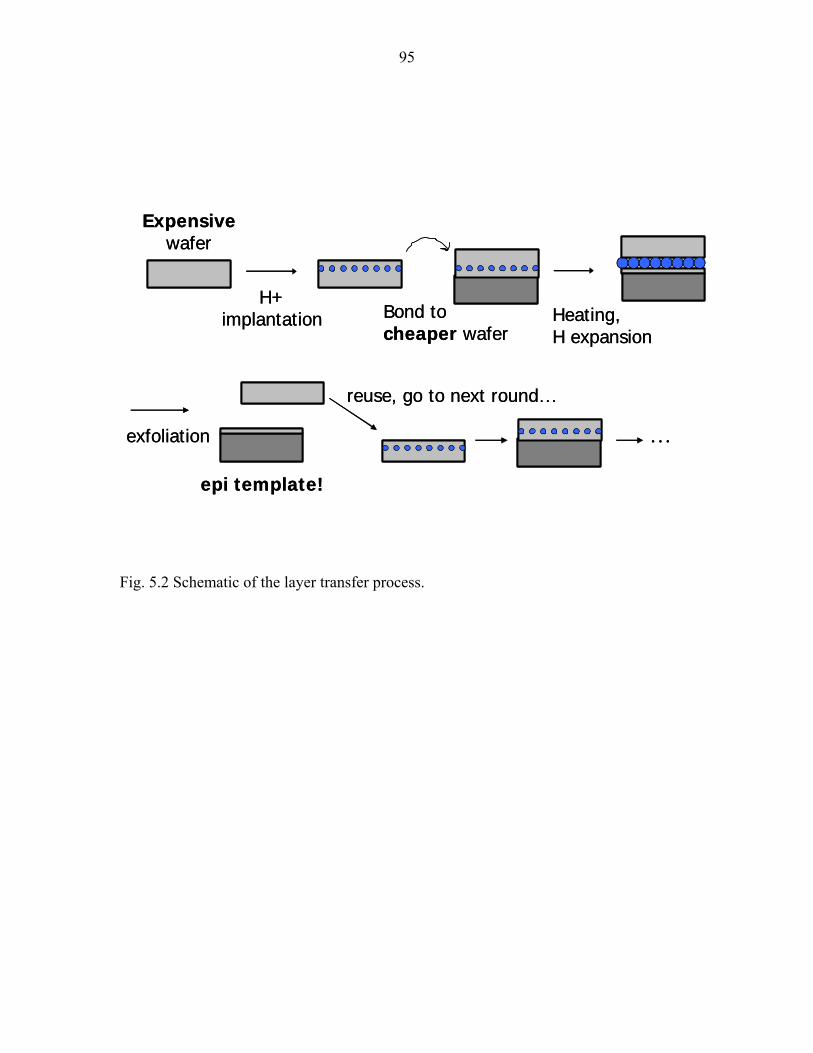
95
epi template!
H+implantation Bond to
cheaper waferHeating,H expansion
reuse, go to next round…
Expensivewafer
Fig. 5.2 Schematic of the layer transfer process.
exfoliation …
epi template!
H+implantation Bond to
cheaper waferHeating,H expansion
reuse, go to next round…
Expensivewafer
…exfoliation

96
Si wafer InP film
Fig. 5.3 Photograph of a layer-transferred InP/Si alternative substrate.

97
Fig. 5.4 Typical AFM topological image for InP surface of the as-transferred InP/Si
alternative substrate.
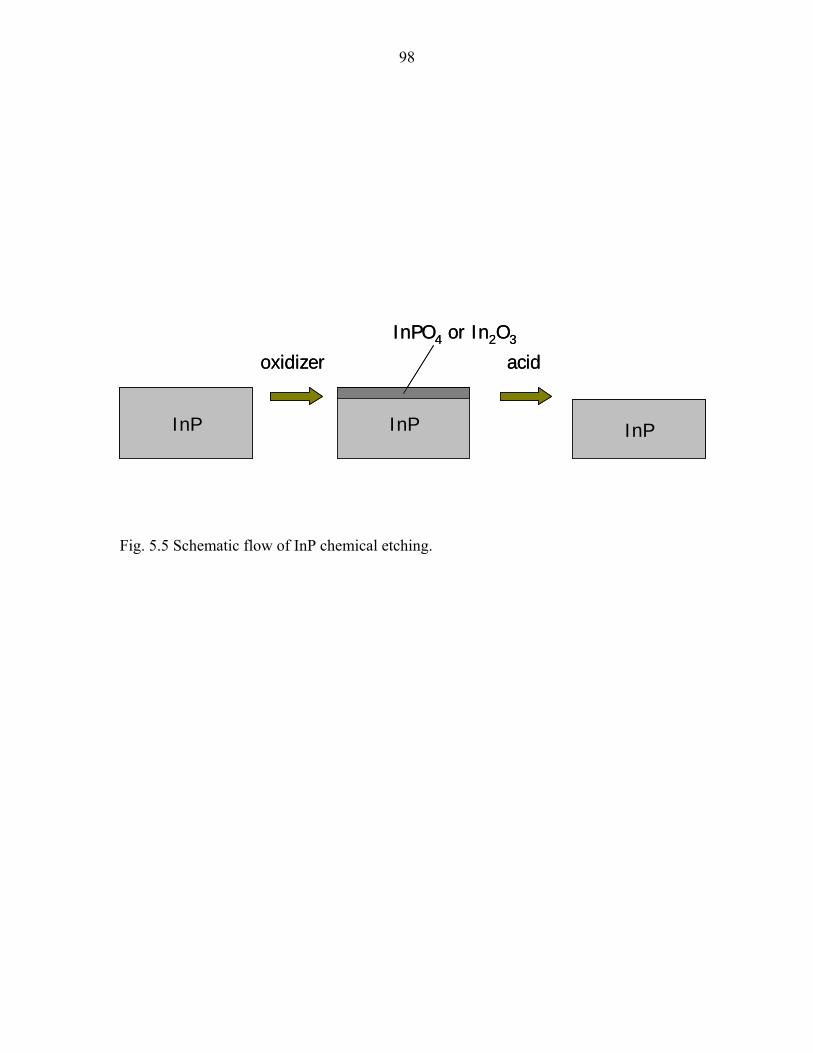
98
InP
InPO4 or In2O3
InP InP
oxidizer acid
InP
InPO4 or In2O3
InP InP
oxidizer acid
Fig. 5.5 Schematic flow of InP chemical etching.

99
CH3COOHH3PO4HCl
H3PO4H2O2HF
CH3COOHH2O2HF
CH3COOHH2O2HCl
H3PO4H2O2HCl
agent 3agent 2agent 1
CH3COOHH3PO4HCl
H3PO4H2O2HF
CH3COOHH2O2HF
CH3COOHH2O2HCl
H3PO4H2O2HCl
agent 3agent 2agent 1
Table 5.1 List of the chemical solutions for InP smoothening used in this study. Agent 1,
2 and 3 are dissolver, oxidizer and diluent, respectively.
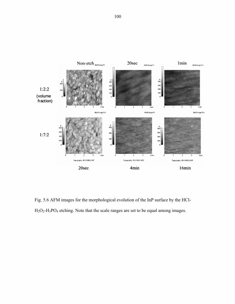
100
1:2:2
1:7:2
Non-etch
4min 16min
Fig. 5.6 AFM images for the morphological evolution of the InP surface by the HCl-
H2O2-H3PO4 etching. Note that the scale ranges are set to be equal among images.
(volumefraction)
20sec 1min
20sec
1:2:2
1:7:2
Non-etch
4min 16min
umefraction)
20sec 1min
20sec
(vol
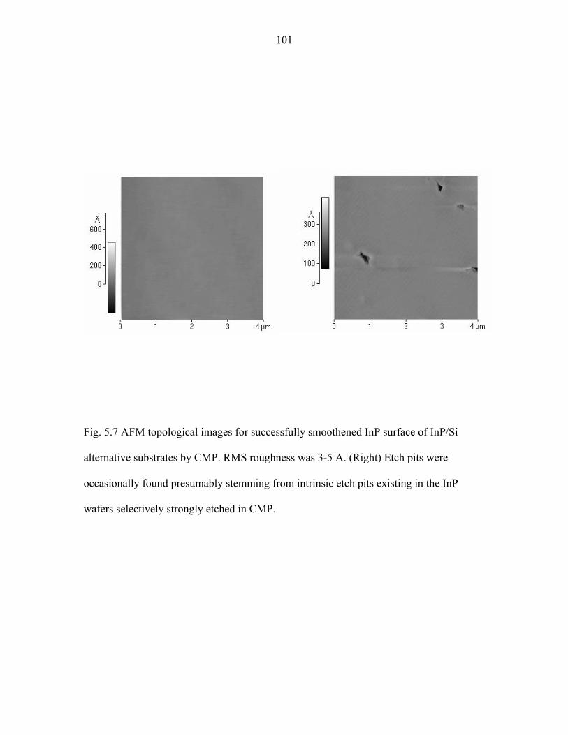
101
Fig. 5.7 AFM topological images for successfully smoothened InP surface of InP/Si
alternative substrates by CMP. RMS roughness was 3-5 A. (Right) Etch pits were
occasionally found presumably stemming from intrinsic etch pits existing in the InP
wafers selectively strongly etched in CMP.
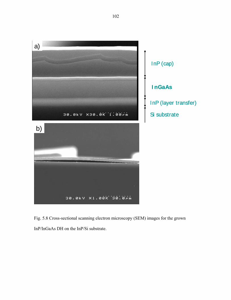
102
InP (cap)
InGaAs
InP (layer transfer)
Si substrate
a)
InP (cap)
InGaAs
InP (layer transfer)
Si substrate
a)
b)b)
Fig. 5.8 Cross-sectional scanning electron microscopy (SEM) images for the grown
InP/InGaAs DH on the InP/Si substrate.

103
b)a)
Fig. 5.9 Optical photographs of an InP/Si substrate etched by HCl-H3PO4-H2O2 (1:2:2
vol.) for 20 sec (a) before and (b) after InP/InGaAs DH growth.
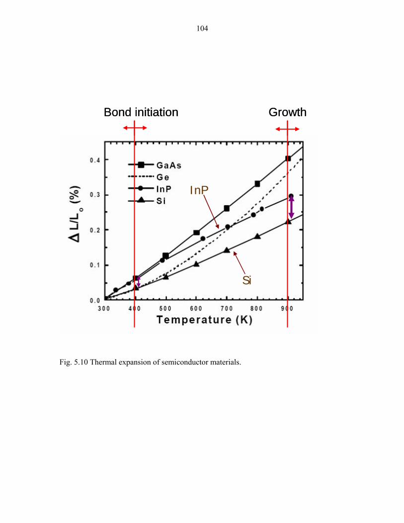
104
Reduce growth T ?Thinner InP?
Bond initiation Growth
Fig. 5.10 Thermal expansion of semiconductor materials.
InP
SiReduce growth T ?Thinner InP?
Bond initiation Growth
InP
Si

105
Fig. 5.11 Optical micrograph of a layer-transferred InP/Si substrate; one-quarter of a 50
mm diameter InP layer was transferred onto a 50 mm diameter Si substrate.

106
Fig. 5.12 Cross-sectional transmission electron microscope image of an InP/Si substrate
fabricated using InP implanted with 115 keV He+ to a dose of 1.0x 1017 cm-2 showing the
strain contrast caused by defects created during ion implantation and (inset) selected-area
diffraction image indicating that the InP adjacent to the bonded interface (within ~200
nm) is crystalline.

107
Chapter 6 InGaAs solar cells grown on InP/SiO2/Si
bonded substrates
6-1. Introduction
In the previous chapter, we successfully fabricated alternative inexpensive InP/SiO2/Si
substrate structures for III-V semiconductor epitaxial growth. Now we are ready to
fabricate III-V semiconductor compound solar cells on very inexpensive substrate, silicon,
using that technology of InP layer transfer. In this study, we grew In0.53Ga0.49As single-
junction solar cells lattice matched to InP on the fabricated InP/SiO2/Si alternative
substrate structures prepared with wafer bonding and layer transfer.
Aim of this study
The aim of the study of this chapter is to demonstrate III-V solar cell growth on the
prepared alternative inexpensive substrates of InP/SiO2/Si and show the validity of the
alternative substrate through characterization of the grown cells compared with reference
cells grown on commercially available epi-ready InP bulk substrates.
6-2. Experimental
To test the performance of III-V compound active photovoltaic device layers grown on
the wafer-bonded InP/Si substrates in functional solar cell structures, single-junction
InGaAs solar cells were grown on both InP/Si substrates and commercial bulk epi-ready
InP (001) substrates as a reference by metal-organic chemical vapor deposition

108
(MOCVD). Each of the solar cells had an n-type In0.53Ga0.47As emitter and a p-type
In0.53Ga0.47As base with bandgap energy of 0.74 eV, nominally lattice-matched to (001)
InP. Although we have not investigated the strain in these epitaxial InGaAs layers in
detail yet, it is supposed that they are under tensile strain due to the difference in thermal
expansion between InP and Si from the analysis with a similar heterostructure in
Reference 1. The cells were designed to enable convenient and low-resistance contact to
both base and emitter through the top surface of the cell. A schematic of the InGaAs cell
structure is shown in Figure 6.1. The cell growth begins with a 1 μm thick InP buffer
layer doped n-type with a target carrier concentration of 1 x 1019 cm-3 that functions as a
current spreading layer for lateral back side contact. Back side and front side contacts
were made using Ti/Au contacts on n-type InGaAs doped with a target carrier
concentration of 1 x 1019 cm-3. Typical optical micrographs of the front contact pads and
grids of the InGaAs solar cells grown on the InP/Si substrates and on bulk InP (001)
substrates are shown in Figure 6.2. An InGaAs tunnel-junction was used to switch the
carrier type from the p-type in the base to n-type in the back side contact structure,
allowing the front and back contacts to be fabricated with a single lithographic process.
The remainder of the structure was typical of a single-junction InGaAs cell consisting of
an InP window layer, a 300 nm thick n-type InGaAs emitter doped with a carrier
concentration of 5 x 1018 cm-3, a 3 μm thick p-type InGaAs base doped with a carrier
concentration of 1 x 1017 cm-3, and a 50 nm thick p-type InP back side field layer doped
with a carrier concentration of 1-2 x 1018 cm-3. No anti-reflective coating was used in the
fabrication of the test cells. A typical image of the InGaAs solar cells grown on the InP/Si
substrate is shown in Figure 6.3.

109
6-3. Results and discussion
Light current-voltage (I-V) characteristics of the InGaAs cells grown on the InP/Si
substrates and on bulk InP (001) substrates were measured under AM1.5 Global
illumination truncated at 850 nm by a long-pass filter, to mimic the optical configuration
of subcells under a GaAs cell. The resulting I-V data are shown in Figure 6.4. The device
parameters for the InGaAs cell grown on the wafer-bonded InP/Si substrate were Jsc =
24.9 mA cm-2, Voc = 0.30 V and FF = 0.66, where Jsc, Voc and FF are short-circuit current,
open-circuit voltage and fill factor, respectively. This performance was comparable to
that of the InGaAs cells grown on bulk InP (001) substrates, Jsc = 21.5 mA cm-2, Voc =
0.31 V and FF = 0.70. Figure 6.5 shows the spectral responses for the InGaAs solar cells
grown on the InP/Si substrate and a bulk InP substrate.
The larger Jsc and the higher quantum efficiency for the cell grown on the InP/Si
substrate are attributed to enhanced light trapping effects in the wafer-bonded cell
structure, due primarily to reflection at the bonding interfaces. Noting the large refractive
index difference at the InP/SiO2/Si bonding interface, nInP ~ 3.5, nSiO2 ~ 1.5 and nSi ~ 3.5
in the IR region, the reflectivity at the InP/SiO2/Si interface was estimated as follows [2].
2
221
221
1 δ
δ
i
i
tot errerrR −
−
++
= , (1)
where
jj
jjj NN
NNr
+−
=−
−
1
1 (2)
and
110
112 dnλπδ = . (3)
The subscript j denotes the layer, where the InP, SiO2 and Si layers correspond to j = 0, 1
and 2, respectively. Note that the refractive indices Nj are generally complex functions of
wavelength and are expressed as jjj iknN += , where both nj and kj are real. λ is the
wavelength in vacuum and the thickness of the SiO2 layer, d1, was set to 420 nm as
determined by ellipsometry measurement. For the optical constants of In0.53Ga0.47As, the
data in Reference 3 was used with a modification of the imaginary part of the dielectric
constant, ε2, fit to the power law around at the absorption edge [4],
( ) ( )( )2
21
2 ωω
ωεh
h gE−∝ . (4)
The bandgap energy Eg of In0.53Ga0.47As was set to be 0.73 eV. The optical constants of
Si, SiO2 and InP were adopted from Reference 5. The reflectivity at the In0.53Ga0.47As/InP
interface was also estimated as a reference simply by determining 1r from Equation 2,
where the In0.53Ga0.47As and InP layers correspond to j = 0 and 1, respectively. Based on
this calculation the reflectivity of the InP/SiO2/Si interface is estimated to be ~0.5 at
maximum in the IR range for normal incidence due to the large refractive index
differences at the InP/SiO2 and SiO2/Si interfaces, as shown in Figure 6.6. On the other
hand, the reflectivity at the In0.53Ga0.47As/InP interface is negligibly small compared with
that at the InP/SiO2/Si bonding interface, as seen in Figure 6.6, due to the small
difference in the refractive indices between In0.53Ga0.47As and InP, nIn0.53Ga0.47As ~ nInP ~
3.5 in the IR region. Particularly the reflectivity of the InP/SiO2/Si interface significantly
increases after 1200 nm, which well explains the enhanced photocurrent for the InGaAs
111
cell grown on the InP/Si substrate relative to that on a bulk InP substrate seen in the
spectral responses of Figure 6.5.
Absorption in the In0.53Ga0.47As layer was also calculated using a one-dimensional
optical computational package [6]. This simulation was performed for a structure
consisting of air/ In0.53Ga0.47As (3650 nm)/ InP (1400 nm)/ SiO2 (420 nm)/ Si for the cell
on the InP/Si substrate and air/ In0.53Ga0.47As (3650 nm)/ InP for the reference cell grown
on a bulk InP substrate. The enhanced photocurrent and the oscillatory variation of the
spectral quantum efficiency for the InGaAs cell on the InP/Si substrate were well-
modeled by a simple one-dimensional optical calculation of the absorbance of the
In0.53Ga0.47As layer in the In0.53Ga0.47As/InP/SiO2/Si structure relative to the
In0.53Ga0.47As/InP reference structure, as shown in Figure 6.5.
Light trapping effects might also be enhanced by the slightly rougher top surface for
cells grown on InP/Si substrates, attributable to the increased roughness of the InP/Si
substrate growth surface (~10 nm-rms), relative to the bulk, epi-ready InP (001)
substrates (<1 nm-rms) [7, 8]. This light I-V characteristic result indicates that the
fabricated InP/Si substrates are promising alternative substrates to InP bulk wafers for
InGaAs solar cell fabrication. The obtained Jsc of 24.9 mA cm-2 for the InGaAs cell on
the InP/Si substrate is large enough to current match to state-of-art InGaP/GaAs two-
junction cells [9, 10]. This InGaAs cell is therefore a strong candidate for the bottom cell
of an ultrahigh efficiency three-junction cell with its significantly higher Voc than the
conventional Ge bottom cell [11-13].

112
6-4. Conclusions
We have demonstrated InGaAs solar cell fabrication on layer-transferred InP/Si
substrates. Such InP/Si substrates could be used as substrates for InGaAsP/InGaAs dual-
junction solar cells lattice-matched to InP as well as conventional InP single-junction
cells. Ultimately, InP/Si substrates are extendable to fabrication of ultrahigh efficiency
four-junction AlInGaP/GaAs/InGaAsP/InGaAs cells via a direct bond interconnect
between subcell structures of InGaAsP/InGaAs grown on InP/Si and AlInGaP/GaAs
grown on GaAs to form the overall four junction cell structure.
6-5. References
[1] A. Fontcuberta i Morral, J. M. Zahler, S. P. Ahrenkiel, M. W. Wanlass, and H. A.
Atwater, Appl. Phys. Lett. 83, 5413, 2003.
[2] O. S. Heavens, Optical Properties of Thin Solid Films, Butterworths Scientific
Publications, London, 1955.
[3] M. A. Afromowitz, Solid State Comm. 15, 59-63, 1974.
[4] S. Adachi, J. Appl. Phys. 66 (12), 6030-6040, 1989.
[5] E. D. Palik, ed., Handbook of Optical Constants of Solids, Academic Press, Orland,
1985.
[6] SpectraRay II, SENTECH Instruments GmbH, 2006.
[7] E. Yablonovitch and G. D. Cody, IEEE Trans. Electron. Devices ED-29, 300, 1982.
[8] J. H. Hu and R. G. Gordon, Solar Cells 30, 437, 1991.
[9] T. Takamoto, E. Ikeda, H. Kurita, and M. Ohmori, Appl. Phys. Lett. 70, 381, 1997.

113
[10] D. B. Jackrel, S. R. Bank, H. B. Yuen, M. A. Wistey, J. S. Harris, A. J. Ptak, S. W.
Johnson, D. J. Friedman, S. R. Kurtz, J. Appl. Phys. 101, 114916, 2007.
[11] D. J. Friedman and J. M. Olson, Prog. Photovolt. 9, 179, 2001.
[12] J. M. Olson, D. J. Friedman, and S. R. Kurtz, in Handbook of Photovoltaic Science
and Engineering, edited by A. Luque and S. Hegedus (Wiley, New York), p. 359, 2003.
[13] R. R. King, R. A. Sherif, G. S. Kinsey, S. R. Kurtz, C. M. Fetzer, K. M. Edmondson,
D. C. Law, H. L. Cotal, D. D. Krut, J. H. Ermer, and N. H. Karam, Proceedings of the
International Conference on Solar Concentrators for the Generation of Electricity or
Hydrogen (NREL, Golden), 2005.

114
n-InGaAs, 0.3μm
p-InP BSF
p-InGaAs, 3μm
InGaAs tunnel junctionInP etch stop
InGaAs contact layerInP buffer
InP, transferredSiO2 bonding layer
Si substrate
n-InP windown-InGaAs
Ti/Pt/Au
Ti/Pt/Au
InP/Sisubstrate
n-InGaAs, 0.3μm
p-InP BSF
p-InGaAs, 3μm
InGaAs tunnel junctionInP etch stop
InGaAs contact layerInP buffer
InP, transferredSiO2 bonding layer
Si substrate
n-InP windown-InGaAs
Ti/Pt/Au
Ti/Pt/Au
InP/Sisubstrate
Fig. 6.1 Schematic cross-sectional view of the InGaAs solar cell grown on the InP/Si
substrates.

115
Fig. 6.2 Optical micrographs of the InGaAs cells, including contact pads and grids,
fabricated on (left) an InP/Si substrate and (right) a bulk InP (001) substrate. The contact
pad on the left is the n-side contact and the pad on the right is the p-side contact.

116
Fig. 6.3 Optical micrograph of the InGaAs solar cells grown on an InP/Si substrate.
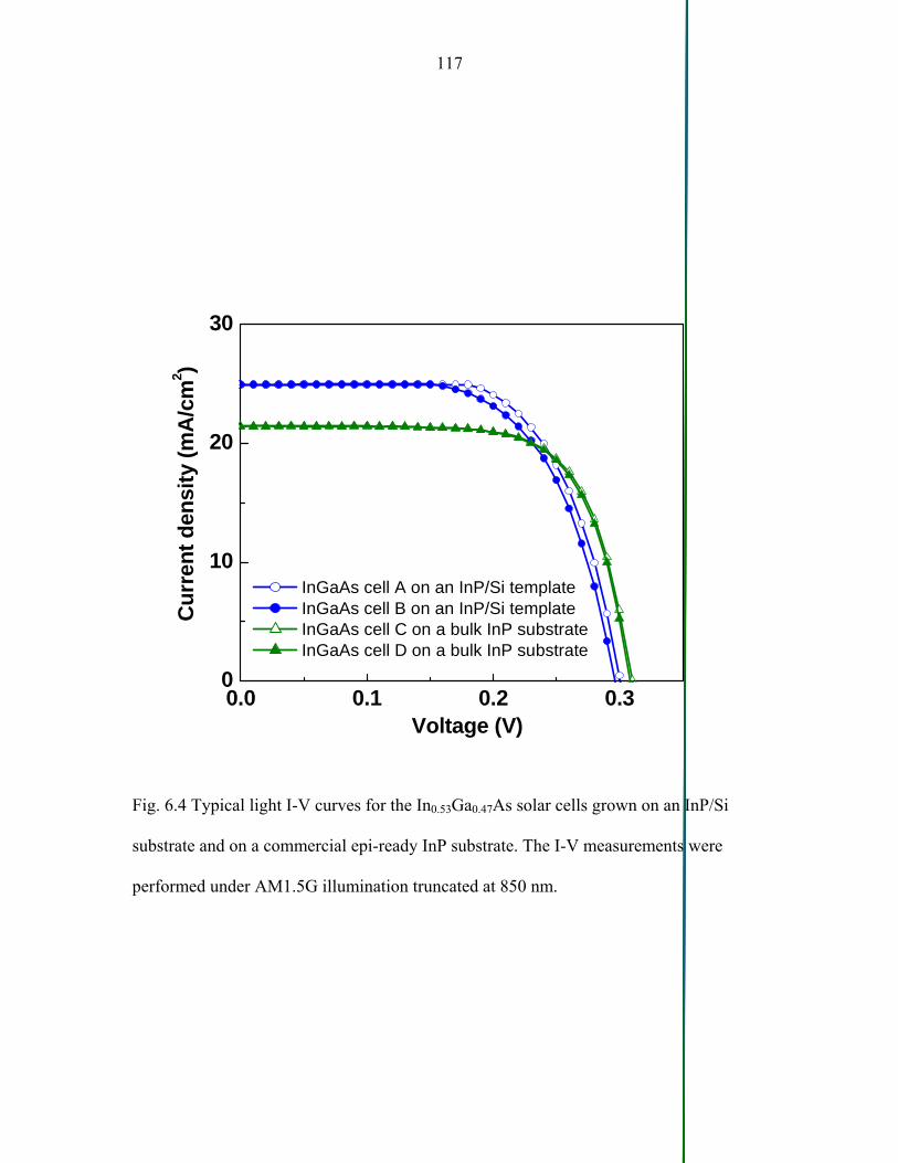
117
Fig. 6.4 Typical light I-V curves for the In0.53Ga0.47As solar cells grown on an InP/Si
substrate and on a commercial epi-ready InP substrate. The I-V measurements were
performed under AM1.5G illumination truncated at 850 nm.
0.0 0.1 0.2 0.30
10
20
30
InGaAs cell A on an InP/Si template InGaAs cell B on an InP/Si template InGaAs cell C on a bulk InP substrate InGaAs cell D on a bulk InP substrate
Cur
rent
den
sity
(mA
/cm
2 )
Voltage (V)
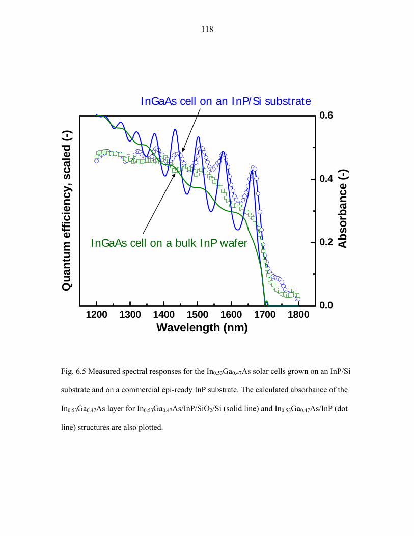
118
InGaAs cell on an InP/Si substrate
1200 1300 1400 1500 1600 1700 1800
Qua
ntum
effi
cien
cy, s
cale
d (-)
Wavelength (nm)
0.0
0.2
0.4
0.6
Abs
orba
nce
(-)
InGaAs cell on a bulk InP wafer
Fig. 6.5 Measured spectral responses for the In0.53Ga0.47As solar cells grown on an InP/Si
substrate and on a commercial epi-ready InP substrate. The calculated absorbance of the
In0.53Ga0.47As layer for In0.53Ga0.47As/InP/SiO2/Si (solid line) and In0.53Ga0.47As/InP (dot
line) structures are also plotted.

119
800 1000 1200 1400 1600 1800
0.0
0.1
0.2
0.3
0.4
0.5 InP/SiO2 420nm/Si In0.53Ga0.47Ag/InP
Ref
lect
ivity
(-)
Wavelength in vacuum (nm)
Fig. 6.6 Calculated reflectivities of the InP/SiO2/Si and In0.53Ga0.47As/InP interfaces.
120
Chapter 7 Plasmonic GaAs Solar Cells
7-1. Introduction
7-1-1. Plasmonics for solar cell applications
Metal nanoparticles are known to exhibit distinctive optical characteristics, such as
surface-enhanced Raman scattering (SERS) and second harmonic generation (SHG),
relative to the bulk form of metals. [1-3] Representatives of the use of metal
nanoparticles are biomolecular manipulation, labeling and detection with SERS. [4, 5]
Other optoelectronic fields inspired by metal nanoparticles are also emerging, such as
multiphoton absorption and fluorescence excitation for microscopy, microfabrication and
optical data storage [6, 7].
These characteristics highly rely on the surface plasmon absorption, an enhanced
absorption of light or electromagnetic fields by coupling between the incident photons
and collective oscillation of free electrons at the metal surface. [8, 9] It was theoretically
suggested that electromagnetic energy can be guided along periodic chain arrays of
closely spaced metal nanoparticles that convert the optical mode into non-radiating
surface plasmons. [10] Such plasmonic devices exploit light localization in the dipole-
dipole coupling, or collective dipole plasmon oscillations of electrons, in neighboring
nanoscale metal particles at the plasmon frequency. Plasmon waveguides consisting of
closely spaced Ag nanoparticles with diameters around 30 nm have been experimentally
observed to guide electromagnetic energy over distances of several hundred nanometers
via near-field particle interactions. [11] Furthermore it has been suggested that light can

121
be routed efficiently around sharp corners of nanoparticle chain arrays. [12] Such
plasmon waveguide technologies can potentially be utilized for construction of all-optical
nanoscale network. [13-15]
Solar cell structures have been suffering from such a trade-off on the thickness of the
active photovoltaic layers as follows. Thinner photovoltaic layers will have less light
absorption while thicker layers will have more bulk carrier recombination, as
schematically depicted in Figure 7.1. Both of these two factors would be losses for the
solar cell electrical output converted from the incident sunlight energy. Therefore the
thickness of the active photovoltaic layer is usually optimized to maximize the energy
conversion efficiency through that trade-off.
Metallic nanostructures can excite surface plasmons and can dramatically increase the
optical path length in thin active photovoltaic layers to enhance overall photoabsorption,
as described in the following sections. This effect has potential for cost and weight
reduction with thinned layers and also for efficiency enhancement associated with
increased carrier excitation level in the absorber layer.
In this study, we have investigated two types of “plasmonic” solar cells described as
follows.
7-1-2. Plasmonic solar cells with metal nanoparticles
122
Metal nanoparticles placed on solar cell surfaces can act as “antennas” to collect the
incident light with their large extinction cross section near the surface plasmon resonance
and then scatter the incident light into a wide range of angles to increase the optical path
length in the absorber layer. This effect has potential for cell cost and weight reduction
resulting from use of thinner absorber layers and also for efficiency enhancement
associated with increased carrier excitation level. Several research groups have observed
photocurrent enhancement for Si cells by this scheme. [16-22] Applications of such
plasmonic metal nanoparticles to other types of solar cells such as dye-sensitized solar
cells and organic solar cells have been also reported. [23-25] No such study however has
been done, to the best of our knowledge, for III-V semiconductor compound solar cells
even though the very same trade-off between the absorption length and the carrier
diffusion length exists also in III-V cells. In this study we specifically investigate the
effect of arrays of subwavelength-size metal particles on GaAs solar cell absorption and
photocurrent.
7-1-3. Plasmonic solar cells with metallic back structures
By placing a metallic layer at the bottom of a photovoltaic layer as schematically
depicted in Figure 7.2, incident light can couple into surface plasmons propagating at the
semiconductor/metal interface via some subwavelength-size feature such as nanoscale
grooves. [15, 26-28] In this way, we can convert the direction of energy flux from normal
to lateral direction relative to the photovoltaic layer. This is a novel concept to utilize
such surface plasmon propagation for solar cell applications to harvest more energy from
the sun in thin photovoltaic active layers. [29]
123
Some types of conventional solar cells such as silicon solar cells also have metallic
back reflectors to increase optical path, while III-V semiconductor compound solar cells
such as GaAs cells have thin photovoltaic active layers on top of thick substrate.
However, the plasmon-induced absorption enhancement by metallic back structures
observed in this study would occur significantly only for strongly absorbing or direct
bandgap semiconductors accounting for the energy dissipation in metals. We calculated
energy dissipation fraction of coupled surface plasmon polaritons propagating at material
interfaces into metals and semiconductors as follows. Electrical energy dissipation
(energy per volume per time) is written as;
( ) ( ) 2
0 ,"21, zxEzxP
rεωε= , (Eq. 1)
where ω is frequency of the field, ε” is imaginary part of relative permittivity or
dielectric function of the medium considered, ε0 is permittivity of vacuum, and E (x, z) is
the electric field. [30] The x-axis and z-axis were taken to be parallel and normal to the
plane of the metal/semiconductor interface, respectively, as schematically shown in
Figure 7.3. In this calculation, I considered semi-infinite thick semiconductor and metal
layers for simplicity. The electric field components are written as follows, with the
subscripts 1 for metal and 2 for dielectric.
( ){ }tzkxkiEE jzxjx ω−−= ,0, exp (Eq. 2)
124
( ){ }tzkxkiEkkE zx
z
xz ω−−−= 1,0
1,1, exp (Eq. 3)
( ){ }tzkxkiEkkE zxz
xz ω−−= 2,0
2,2, exp (Eq. 4)
( )2,1=j
Since E (x, j) and E (z, j) are in phase,
2
,
2
,
2
jzjxj EEE +=r
. (Eq. 5)
Decomposing the complex wavenumbers k into their real and imaginary parts,
( ){ }( ) ( ) ( ){ }tzkxkizkxkE
tzkxkiEE
jzxjzx
jzxjx
ω
ω
−−−−=
−−=
''exp"exp"exp
exp
,,0
,0, , (Eq. 6)
( ){ }
( ) ( ) ( ){ }tzkxkizkxkEkk
tzkxkiEkkE
zxzxz
x
zxz
xz
ω
ω
−−−−−=
−−−=
''exp"exp"exp
exp
1,1,01,
1,01,
1,
, (Eq. 7)
( ){ }
( ) ( ) ( ){ }tzkxkizkxkEkk
tzkxkiEkkE
zxzxz
x
zxz
xz
ω
ω
−−−−=
−−=
''exp"exp"exp
exp
2,2,02,
2,02,
2,
. (Eq. 8)
From Equations 5-8,
125
( ) ( zkxkEkkEEE zx
z
xzx "2exp"2exp1 1,
20
2
1,
21,
21,
2
1 −−⎟⎟
⎠
⎞
⎜⎜
⎝
⎛+=+=
r ) , (Eq. 9)
( ) ( zkxkEkkEEE zxz
xzx "2exp"2exp1 2,
20
2
2,
22,
22,
2
2 −−⎟⎟
⎠
⎞
⎜⎜
⎝
⎛+=+=
r ) . (Eq. 10)
The energy dissipation at the interface (energy per area per time) for each side of material
is therefore written as;
( ) ( )
( ) ( )∫
∫∞
∞
−−⎟⎟
⎠
⎞
⎜⎜
⎝
⎛+=
=
0 ,2
0
2
,0
0
2
0
"2exp"2exp1"21
,"21
dzzkxkEkk
dzzxExP
jzxjz
xj
jjj
εωε
εωεr
. (Eq. 11)
Then energy dissipation fraction for the dielectric or semiconductor material is;
( )
( ) ( )∫∫
∫
∞∞
∞
−⎟⎟
⎠
⎞
⎜⎜
⎝
⎛++−⎟
⎟
⎠
⎞
⎜⎜
⎝
⎛+
−⎟⎟
⎠
⎞
⎜⎜
⎝
⎛+
=+
0 2,
2
2,20 1,
2
1,1
0 2,
2
2,2
21
2
"2exp1""2exp1"
"2exp1"
dzzkkkdzzk
kk
dzzkkk
PPP
zz
xz
z
x
zz
x
εε
ε
. (Eq. 12)
This energy dissipation fraction is simplified by using
1
2
2
1, εε
=z
x
kk (Eq. 13)

126
and
2
1
2
2, εε
=z
x
kk , (Eq. 14)
which are derived from
21
21
21⎟⎟⎠
⎞⎜⎜⎝
⎛+
=εεεεω
ckx (Eq. 15)
and
222
, ⎟⎠⎞
⎜⎝⎛=+
ckk jxjz
ωε . (Eq. 16) [31]
The semi-infinite integrals in Equation 12 are conducted as;
( )"2
1"2exp,
0 ,jz
jz kdzzk =−∫
∞. (Eq. 17)
From Equations 13, 14 and 17, Equation 12 is simplified into;
127
⎟⎟⎠
⎞⎜⎜⎝
⎛++⎟⎟
⎠
⎞⎜⎜⎝
⎛+
⎟⎟⎠
⎞⎜⎜⎝
⎛+
=+
2
1
2,
2
1
2
1,
1
2
1
2,
2
21
2
1"2
"1"2
"
1"2
"
εεε
εεε
εεε
zz
z
kk
kPP
P . (Eq. 18)
Using this formalism, the energy dissipation fraction in the semiconductor layer from
the surface plasmons propagating at the semiconductor/metal interface was calculated for
several combinations of semiconductors and metals, as shown in Figure 7.4. The
wavelength dependent data of the dielectric functions of metals and semiconductors of
Palik was used for this calculation. [32] It is found from this result that most energy is
absorbed by GaAs rather than metals for the visible optical wavelength range, which
solar cell applications concerns, particularly for the cases with Ag and Al. This means
GaAs can effectively harvest the energy extracted from the coupled surface plasmons
beating the Ohmic loss in metals with its strong absorption or large imaginary part of
dielectric function. On the other hand, silicon, which is a weak absorber, has much lower
energy absorption fraction suffering from Ohmic loss in metals. This is a great benefit for
direct bandgap semiconductor materials, which are stronger absorbers, for such types of
“plasmonic” solar cell applications.
7-2. Plasmonic GaAs solar cells with metal nanoparticle arrays
7-2-1. Experimental
Optically thin GaAs solar cells
To demonstrate absorption enhancement by metal nanoparticle scattering, ‘optically
thin’ GaAs solar cells (i.e., absorber layer thickness << absorption length) with a 50nm-
128
thick p-type emitter on top of a 150nm-thick n-type base were grown by metalorganic
chemical vapor deposition. Dense arrays of metal nanoparticles were then deposited onto
the Al0.8Ga0.2As window layer of the GaAs cells through porous alumina membranes by
thermal evaporation. A schematic of the optically thin GaAs cell structure is shown in
Figure 7.5. This cell structure consisted of a 50nm-thick p-type emitter on top of a
150nm-thick n-type base epitaxially grown on a (001) n-type GaAs substrate by
metalorganic chemical vapor deposition (MOCVD). The remainder of the structure was
typical of a single-junction GaAs solar cell consisting of a 30 nm thick p-type
Al0.8Ga0.2As window layer and a 500 nm thick n-type Al0.8Ga0.2As back side field (BSF)
layer. Front and back side electrical contacts were made using 150 nm thick Au contacts
formed by thermal evaporation with a standard optical lithography for the front contact.
No anti-reflective coating was used in the fabrication of the cell structure.
Metal nanoparticle arrays
Dense arrays of metal nanoparticles were deposited onto the window layers for both
types of the GaAs solar cells through porous alumina (Al2O3) membranes by thermal
evaporation. The electrochemical fabrication of the porous membranes [33, 34] and metal
nanoparticle deposition were conducted by Keisuke Nakayama of Caltech. Details of the
porous alumina membrane preparation and characterization are described somewhere else.
[35] The Ag particle diameter ranged from 60-150 nm, and interpartice spacing ranged
from 100-300 nm, with particle shape in the form of upright circular cylinders. The Ag
nanoparticle dimensions were quite uniform across each cell sample due to the uniformity
of the pore size and spacing in the alumina membranes, for which pore diameters were

129
carefully controlled during the membrane preparation. The height of the metal
nanoparticles was controlled simply with the deposition thickness in the thermal
evaporation process. Figure 7.6 shows scanning electron microscope (SEM) images of
the Ag nanoparticle arrays with a diameter of 60 nm and heights ranging through 10 nm
to 75 nm deposited on the GaAs solar cells.
In this way, we obtained quite uniform, dense arrays of metal nanoparticles. We can
control the particle diameter and spacing by the fabrication conditions of the porous
membranes, and particle height simply by deposition thickness. All previously reported
studies for solar cells with metal nanoparticles [16-25] simply used thermal annealing
after evaporation of thin metal films to form metal nanoparticles through thermal
aggregation. Relative to this method, the advantages of our metal nanoparticle fabrication
scheme are represented by the excellent uniformity and controllability for the particle
shape and size and no need for post annealing.
Characterization of the metal nanoparticles and the cells
Spectral response measurements for the fabricated “optically-thin” GaAs solar cells
with and without metal nanoparticles of Ag and Al were taken to determine the effect of
metal nanoparticles. Transmission measurements for the Ag and Al nanoparticles were
obtained from samples deposited on glass slides whose dimensions were similar to those
used for the cell measurements.
7-2-2. Optical model

130
To understand the role of the metal nanoparticles on the GaAs solar cells thoroughly, a
simple optical model to represent the absorption enhancement in the photovoltaic layers
with metal nanoparticles on top has been developed. As an overview, we calculated the
absorbance in the GaAs cells considering scattering and absorption by the metal particles,
accounting the particles’ surface coverage, reflectivity at the air/GaAs interface, angular
dependence of scattered light, extinction efficiency factor, which is extinction cross-
section of the particles normalized by the geometrical cross-section (means how large the
incident light feels for the particles), and radiation efficiency, which represents how much
light interacting with the particles is scattered rather than being absorbed. We calculated
these factors for oblate spheroid particles in the quasistatic limit using an effective
medium approximation accounting for the influence of both air and GaAs. The
calculation details follow.
For simplification, we considered only GaAs photovoltaic layer neglecting the AlGaAs
window layer. (Note that the refractive indices of GaAs and AlGaAs are similar.)
Absorption fraction of the incident light in a GaAs layer with a thickness of L is simply;
( ) ( )( LA )λαλ −−= exp10 , (Eq. 19)
where α is the absorption constant of GaAs and λ is the wavelength in vacuo. The
angular distribution of the light intensity scattered by sub-wavelength sized particles in
the quasistatic limit is known to be;
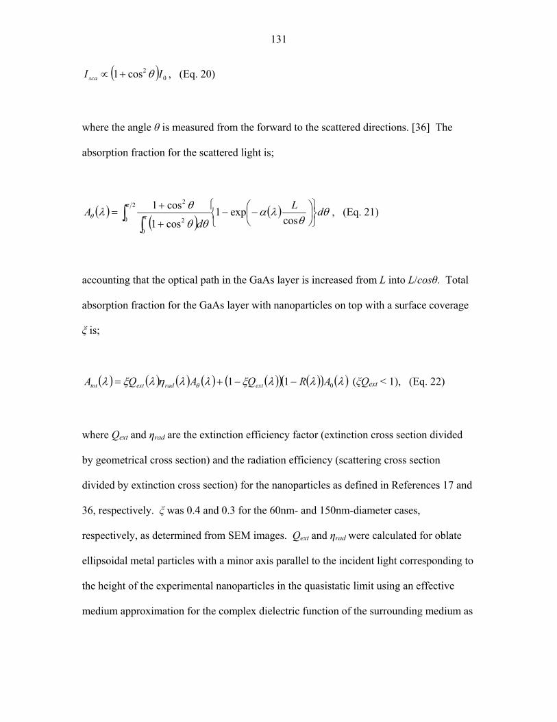
131
( ) 02cos1 II sca θ+∝ , (Eq. 20)
where the angle θ is measured from the forward to the scattered directions. [36] The
absorption fraction for the scattered light is;
( )( )
( ) θθ
λαθθ
θλπ
πθ dL
dA
⎭⎬⎫
⎩⎨⎧
⎟⎠⎞
⎜⎝⎛−−
+
+= ∫
∫ cosexp1
cos1
cos12
0
0
2
2
, (Eq. 21)
accounting that the optical path in the GaAs layer is increased from L into L/cosθ. Total
absorption fraction for the GaAs layer with nanoparticles on top with a surface coverage
ξ is;
( ) ( ) ( ) ( ) ( )( ) ( )( ) ( )λλλξλληλξλ θ 011 ARQAQA extradexttot −−+= (ξQext < 1), (Eq. 22)
where Qext and ηrad are the extinction efficiency factor (extinction cross section divided
by geometrical cross section) and the radiation efficiency (scattering cross section
divided by extinction cross section) for the nanoparticles as defined in References 17 and
36, respectively. ξ was 0.4 and 0.3 for the 60nm- and 150nm-diameter cases,
respectively, as determined from SEM images. Qext and ηrad were calculated for oblate
ellipsoidal metal particles with a minor axis parallel to the incident light corresponding to
the height of the experimental nanoparticles in the quasistatic limit using an effective
medium approximation for the complex dielectric function of the surrounding medium as

132
( ) ( ) ( )3
2 λελελε GaAsair
medium+
= . [36] The wavelength-dependent complex dielectric
functions of metals and GaAs were obtained from Reference 32. Particularly for Al
nanoparticles, Qext and ηrad were calculated for concentric Al-Al2O3 core-shell ellipsoidal
particles with an Al2O3 shell thickness of 4 nm accounting for surface oxidation of Al
particles in the atmosphere. [37, 38] The reflectivity R at the air/GaAs interface is also
accounted as follows since our GaAs solar cells had no anti-reflective coating or surface
structure. Assuming normal incidence of light into a GaAs layer, the wavelength-
dependent reflectivity is written as;
( ) ( )( )
( ) ( )( ) ( )
2
12
12
0 λλλλ
λλ
λNNNN
II
R r
+−
=≡ , (Eq. 23)
where N is the complex refractive index of air or GaAs. Then we took the ratio of the
absorbance of Equation 22 to the absorbance without particle to compare with the
normalized photocurrent data.
7-2-3. Results and Discussion
Figure 7.7 shows the photocurrent spectra for the GaAs solar cells with metal
nanoparticles of Ag and Al on top. This photocurrent data is normalized by the spectral
response of the reference GaAs cell without metal nanoparticles. The maximum
photocurrent enhancement of 260% is seen around at 900 nm for the GaAs cell with Ag
nanoparticles with a diameter of 150 nm, a height of 20 nm and 30% surface coverage.
The normalized photocurrent (J/J0) is seen to be significantly higher for the cells with

133
150nm-diameter nanoparticles relative to those with a 60nm-diameter for almost entire
spectral range, which can be attributed to the considerably higher radiation efficiency, the
ratio of the scattering cross-section to the extinction cross-section, for larger metal
nanoparticles as discussed in a following section.
The transmission spectra for the Ag nanoparticle arrays with a particle diameter of 60
nm and various particle heights deposited on glass slides is shown in Figure 7.8. Surface
plasmon resonance in the metal nanoparticles is seen as the dips around at 400-500 nm,
while no notable scattering is observed for near-IR region. In Figure 7.7, a dip
presumably due to plasmon resonance for the cell with 60nm-diameter Ag particles is
seen around at 600 nm, whose discrepancy from the transmission spectra is attributed to
the effect of different substrates where GaAs has higher refractive index than glass to
redshift the resonant frequency. The dip around at 350 nm for Ag nanoparticle arrays is
due to absorption by interband transitions in Ag.
The computed normalized absorption spectra for GaAs solar cells with metal
nanoparticles are superposed to the experimental normalized photocurrent for the
corresponding cells in Figure 7.7. This model calculation well reproduces the
experimental results qualitatively, including the peaks around at 300 nm and 900 nm and
the dips around at 600 nm for 60nm-diameter Ag and 350 nm for 60nm-diameter Al. The
dip around at 600 nm in the normalized photocurrent for the cell with 60nm-diameter Ag
particles, presumably due to the surface plasmon resonance in the Ag particles, is not
seen for 150nm-diameter. This experimental result is attributed to the significantly higher
134
ηrad (~0.9) for the 150nm-diameter case than that (~0.6) for the 60nm-diameter case
suppressing the absorption loss in the Ag nanoparticles, as shown in Figure 7.9. For both
of Ag and Al, higher photocurrent enhancement at 900 nm for 150nm-diameter cases
than for 60nm-diameter cases is reproduced in the modeling, caused mainly by the higher
Qext for the larger metal nanoparticles. It is important to note that both Ag and Al particle
cells suffer from the loss back scattering from metal nanoparticles into the air as seen in
Equation 20.
Based on these investigations, we have obtained enhancements in net photocurrent, not
only for longer wavelength range, and efficiency for certain optimized conditions, as
shown in Figure 7.10.
7-3. Plasmonic GaAs solar cells with metallic back structures
7-3-1. Experimental
Fabrication of the waveguide-like GaAs solar cell structure with a metal back layer,
schematically shown in Figure 7.11 (a), started with an “inversely grown” GaAs cell
shown in Figure 7.11 (b). This cell structure consisted of a 50nm-thick n-type base on top
of a 50nm-thick p-type emitter epitaxially grown on a (001) p-type GaAs substrate by
MOCVD. The remainder of the structure was typical of a single-junction GaAs solar cell
consisting of a 30 nm thick p-type In0.49Ga0.51P window layer and a 30 nm thick n-type
In0.49Ga0.51P BSF layer. This heavily doped In0.49Ga0.51P BSF layer acts also as the
electrical contact layer to the Ag back reflector layer.
135
A 500 nm thick Ag bonding layer was deposited by thermal evaporation on the
In0.49Ga0.51P BSF layer after removing the 3 um thick GaAs layer from the inversely
grown GaAs cell structure in Figure 7.11 (b) using selective chemical etching with citric
acid (50% weight aqueous solution) - H2O2 solution (4:1 vol.) at room temperature (~10
min). This cell structure with an Ag layer was then bonded to an Ag/Cr/Si supporting
substrate consisting of a heavily doped p-type Si (001) substrate with a 5 nm thick Cr
adhesion layer and a 500 nm thick Ag bonding layer deposited by sequent thermal
evaporation. This wafer bonding technique is based on our investigation presented in
References 39 and 40 and conducted under ~0.5 MPa uniaxial pressure at 200 Co for 10
hours. Then the GaAs substrate was removed by selective chemical etching with H3PO4 -
H2O2 (3:7 vol.) at 50 Co for ~1 hour followed by H3PO4 - H2O2 - H2O (1:4:5 vol.) at room
temperature for ~1 hour. The solution compositions were chosen to maximize the etching
rate of GaAs for the 3:7 solution and the etching selectivity between GaAs and InGaP for
the 1:4:5 solution. [41, 42] The InGaP etch stop layer was then removed by HCl (conc.)
at room temperature for ~1 min. Front and back side electrical contacts were made using
150 nm thick Au contacts formed by thermal evaporation with a standard optical
lithography for the front contact. No anti-reflective coating was used in the fabrication of
the cell structure.
A reference cell structure, shown in Figure 7.11 (c), is also prepared without removal of
the 3 um thick GaAs layer, which mimics an absorbing substrate. For this reference cell
structure, 500 nm thick Ag was deposited on the 3 μm thick GaAs layer and then bonded
to the Ag/Cr/Si substrate followed by similar cell processes as the waveguide-like cell.

136
Figure 7.12 shows a cross-sectional SEM image for the fabricated waveguide-like GaAs
solar cell with an Ag back layer. Figure 7.13 shows photographs of the waveguide-like
GaAs solar cell with an Ag back layer and the reference cell with a 3 μm GaAs absorbing
layer. The waveguide-like cell surface looks reddish to our eyes presumably due to back
reflection of incident light unabsorbed in the GaAs cell by the Ag layer, while the
reference cell surface is dark gray, typical for optically-thick GaAs solar cells.
Figure 7.14 shows AFM and SEM images of the surface of the InGaP BSF layer after
removal of the 3 μm thick GaAs layer, which represents the roughness at the GaAs cell /
Ag interface. This semiconductor/metal interface had a subwavelength-size roughness,
with a peak-valley amplitude around 20 nm, so we expect coupling of the incident light
into surface plasmon mode or photonic waveguide mode by multiple angle scattering to
enhance absorption.
7-3-2. Results and Discussion
Figure 7.15 shows the typical light I-V curves for the waveguide-like GaAs cells with
Ag back structure and the reference GaAs cells under AM1.5 Global solar spectrum with
1-sun total intensity (100 mW cm-2). The short circuit current is significantly larger for
the cells with Ag back structure. Incidentally, the open-circuit voltage varied due to
random shunting, because we have not optimized the process conditions yet, but it does
not affect short-circuit current much. Figure 7.16 shows the normalized photocurrent
spectrum, which is the photocurrent of the waveguide-like cell divided by the
137
photocurrent of the reference cell. These light I-V and spectral response results show that
the waveguide-like GaAs cell obtained overall photocurrent enhancement for entire
wavelengths. A large peak around at 900 nm, the GaAs bandedge, seen in Figure 7.16 is
presumably due to multiple-angle reflection at the Ag back layer. Figure 7.16 also shows
another peak at 600 nm. Figure 7.17 shows the calculated dispersion relation at the
GaAs/Ag interface and surface plasmon resonance is found at 600 nm, represented by the
maximum of the wavevector parallel to the interface. One possible cause of this 600 nm
peak is therefore surface plasmon resonance at the GaAs/Ag interface leading to
absorption enhancement through incoupling of the incident light into propagating surface
plasmon polaritons as described in Section 7-1-3. However, as we also calculated the
absorption enhancement by Fabry-Perot effect in the thin active GaAs layer with
reflecting back surface, a peak for the normalized absorbance is also found around at 600
nm, as seen in Figure 7.18. Due to this coincidence, we cannot determine which effect
caused this 600 nm peak for the photocurrent enhancement for now. This question would
be figured out by switching the metal from Ag into Al to shift plasmon resonance, or
changing cell thickness to shift the Fabry-Perot peak for example.
Significantly, the waveguide structure solar cells presented in this chapter consist of
III-V semiconductor compound materials as thin as a couple of hundreds nanometers,
which indicates a possibility of significant production cost reduction relative to
conventional III-V solar cells. Although the GaAs substrates were wasted by the etch
back process after wafer bonding in this work, the layer transfer technologies developed
in Chapters 5 and 6 could be employed to reuse a single GaAs substrate repeatedly.
138
7-4. Conclusions
In this chapter two types of “plasmonic” GaAs solar cell were investigated. Firstly,
absorption enhancement by metal nanoparticle scattering in ‘optically thin’ GaAs solar
cells was shown. Dense arrays of metal nanoparticles were deposited directly onto the
Al0.8Ga0.2As window layer of the GaAs cells through porous alumina membranes by
thermal evaporation. Spectral response measurements revealed photocurrent
enhancements up to 260% at 900 nm for a GaAs cell with Ag nanoparticles with 150 nm
diameter, 20 nm height and 30% surface coverage, relative to reference GaAs cells with
no metal nanoparticle array. This photocurrent enhancement and the spectral behavior of
the normalized photocurrent are qualitatively reproduced by a simple optical model
representing surface plasmon resonance of metal nanoparticles and multi-angle scattering.
Particularly, larger subwavelength-size metal particles resulted in larger photocurrent due
to higher radiation efficiencies both for Ag and Al. Secondly, waveguide-like GaAs solar
cells with metallic back structures were introduced. Ultrathin GaAs cells with Ag back
layers were fabricated through wafer bonding and layer transfer with selective etch back
of the GaAs substrates. This waveguide-like GaAs cell showed net photocurrent
enhancement throughout the solar spectral range relative to the reference GaAs cell with
an absorbing GaAs back layer. A large peak for the normalized photocurrent around at
the GaAs bandedge was found and attributed to multiple-angle reflection at the Ag back
layer. A smaller peak was found at 600 nm and is due either to surface plasmon coupling
or Fabry-Perot resonance effect.
139
7-5. References
[1] C. K. Chen et al, Phys. Rev. Lett. 46, 145, 1981.
[2] A. Wokaun et al, Phys. Rev. B 24, 849, 1981.
[3] F. J. Garcia-Vidal and J. B. Pendry, Phys. Rev. Lett. 77, 1163, 1996.
[4] Y. W. C. Cao et al, Science 297, 1536, 2002.
[5] W. Fritzsche and T. A. Taton, Nanotechnology 14, R63, 2003.
[6] W. Wenseleers et al, J. Phys. Chem. B 106, 6853, 2002.
[7] X. Yin et al, Appl. Phys. Lett. 81, 3663, 2002.
[8] S. A. Maier and H. A. Atwater, J. Appl. Phys. 98, 011101, 2005.
[9] H. A. Atwater, Sci. Am., p. 56, April, 2007.
[10] M. Quinten et al, Opt. Lett. 23, 1331, 1998.
[11] S. A. Maier et al, Nat. Mater. 2, 229, 2003.
[12] S. A. Maier et al, Mater. Sci. Eng. C 19, 291, 2002.
[13] W. L. Barnes et al, Nature 424, 824, 2003.
[14] L. Dobrzynski et al, Phys. Rev. E 69, 035601, 2004.
[15] D. Pacifici et al, Nat. Photo. 1, 402, 2007.
[16] H. R. Stuart and D. G. Hall, Appl. Phys. Lett. 69, 2327, 1996.
[17] H. R. Stuart and D. G. Hall, Appl. Phys. Lett. 73, 3815, 1998.
[18] D. M. Schaadt et al, Appl. Phys. Lett. 86, 063106, 2005.
[19] S. Pillai et al, Appl. Phys. Lett. 88, 161102, 2006.
[20] D. Derkacs et al, Appl. Phys. Lett. 89, 093103, 2006.
[21] K. R. Catchpole and S. Pillai, J. Appl. Phys. 100, 044504, 2006.
[22] S. Pillai et al, J. Appl. Phys. 101, 093105, 2007.

140
[23] M. Ihara et al, J. Phys. Chem. B 101, 5153, 1997.
[24] C. Wen et al, Sol. Ener. Mat. Sol. Cell. 61, 339, 2000.
[25] B. P. Rand et al, J. Appl. Phys. 96, 7519, 2004.
[26] H. J. Lezec and T. Thio, Opt. Exp. 12, 3629, 2004.
[27] G. Gay et al, Nat. Phys. 2, 262, 2006.
[28] L. Chen et al, Opt. Exp. 14, 12629, 2006.
[29] V. E. Ferry et al, MRS Spring Meeting, San Francisco, L3.2, Mar. 2008.
[30] A. D. Yaghjian, IEEE Trans. Ant. Prop. 55, 1495, 2007.
[31] H. Raether, Surface Plasmons on Smooth and Rough Surfaces and on Gratings,
Springer-Verlag, 1986.
[32] E. D. Palik, ed., Handbook of Optical Constants of Solids (Academic Press, Orland),
1985.
[33] H. Masuda and M. Satoh, Jpn. J. Appl. Phys. 35, L126-L129, 1996
[34] H. Masuda et al, Adv. Mater. 12 (14), 1031-1033, 2000
[35] K. Nakayama, K. Tanabe and H. A. Atwater, in preparation.
[36] C. F. Bohren and D. R. Huffman, Absorption and Scattering of Light by Small
Particles (Wiley, New York), 1983, Chap. 3 and 5.
[37] L. P. H. Jeurgens et al, Appl. Surf. Sci. 144-145, 1999, pp. 11-15.
[38] W. Zhu et al, Appl. Phys. Lett. 78, 2001, pp. 3103-3105.
[39] K. Tanabe et al, Appl. Phys. Lett. 89, 2006, pp. 102106-1-102106-3
[40] K. A. Diest, M. J. Archer, J. A. Dionne, Y. Park, M. J. Czubakowski and H. A.
Atwater, submitted.
[41] Y. Mori and N. Watanabe, J. Electrochem. Soc. 125, 1510-1514, 1978.

141
[42] Y. C. Hsieh et al, J. Cryst. Growth 289, 96-101, 2006.
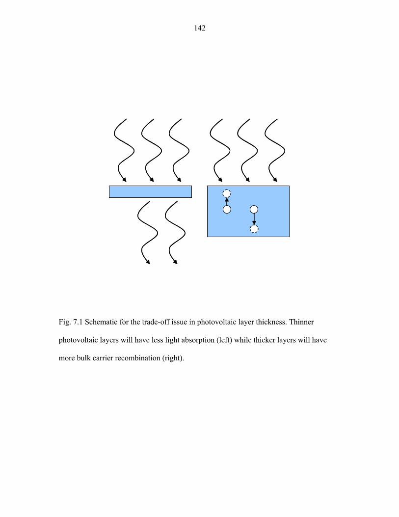
142
Fig. 7.1 Schematic for the trade-off issue in photovoltaic layer thickness. Thinner
photovoltaic layers will have less light absorption (left) while thicker layers will have
more bulk carrier recombination (right).

143
active semiconductor
substrate
metal layer
active semiconductor
substrate
metal layer
Fig. 7.2 Schematic cross-sectional of a solar cell structure with a back metal layer. The
incident light is incoupled into surface plasmons propagating at the semiconductor/metal
interface via subwavelength-size grooves to increase the optical path by switching the
light direction from normal to the photovoltaic layer to lateral.

144
1 metal
2 dielectric
z
(x > 0)
0x
1 metal
2 dielectric
z
(x > 0)
0x
Fig. 7.3 Schematic of the layer configuration considered for the energy dissipation
calculation.
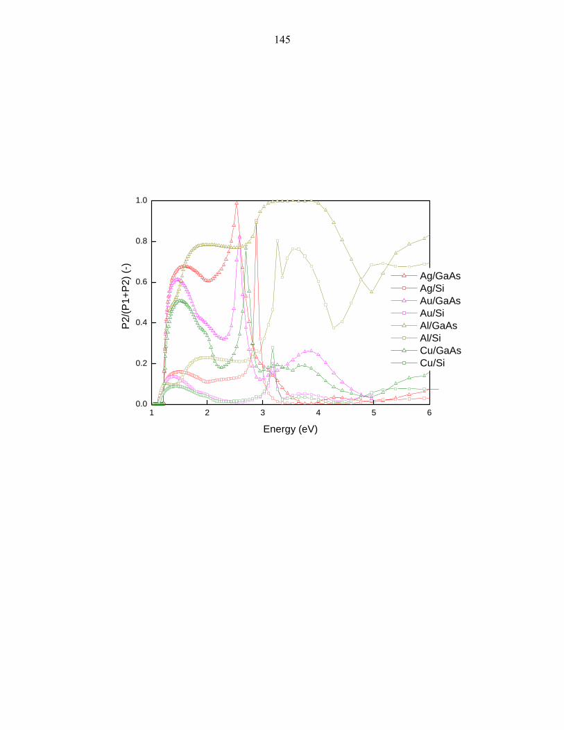
145
1 2 3 4 5 60.0
0.2
0.4
0.6
0.8
1.0
P2/
(P1+
P2)
(-)
Energy (eV)
Ag/GaAs Ag/Si Au/GaAs Au/Si Al/GaAs Al/Si Cu/GaAs Cu/Si
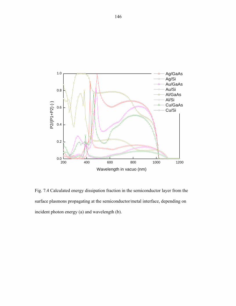
146
200 400 600 800 1000 12000.0
0.2
0.4
0.6
0.8
1.0
P2/
(P1+
P2)
(-)
Wavelength in vacuo (nm)
Ag/GaAs Ag/Si Au/GaAs Au/Si Al/GaAs Al/Si Cu/GaAs Cu/Si
Fig. 7.4 Calculated energy dissipation fraction in the semiconductor layer from the
surface plasmons propagating at the semiconductor/metal interface, depending on
incident photon energy (a) and wavelength (b).

147
GaAs30nm Al0.8Ga0.2As window (Zn 1x1018cm-3)
50nm GaAs emitter (Zn 4x1018cm-3)150nm GaAs base (Si 2x1017cm-3)
500nm Al0.8Ga0.2As BSF (Si 2x1018cm-3)1um GaAs buffer (Si 2x1018cm-3)
GaAs substrate (Si ~1x1018cm-3)
Au
Au
GaAs30nm Al0.8Ga0.2As window (Zn 1x1018cm-3)
50nm GaAs emitter (Zn 4x1018cm-3)150nm GaAs base (Si 2x1017cm-3)
500nm Al0.8Ga0.2As BSF (Si 2x1018cm-3)1um GaAs buffer (Si 2x1018cm-3)
GaAs substrate (Si ~1x1018cm-3)
Au
Au
Fig. 7.5 Schematic cross-sectional diagram of the optically thin GaAs solar cell structure.
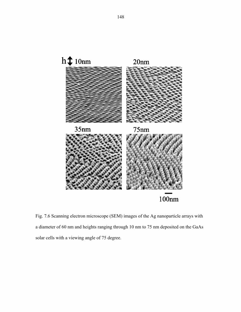
148
100nm
10nm 20nm
35nm 75nm
h
100nm
10nm 20nm
35nm 75nm
100nm
10nm 20nm
35nm 75nm
h
Fig. 7.6 Scanning electron microscope (SEM) images of the Ag nanoparticle arrays with
a diameter of 60 nm and heights ranging through 10 nm to 75 nm deposited on the GaAs
solar cells with a viewing angle of 75 degree.

149
0
0.5
1
1.5
2
2.5
3
200 400 600 800 1000Wavelength (nm)
Nor
mal
ized
pho
tocu
rren
t J/J
0 (-
) Ag d=60nm, h=35nmAg d=150nm, h=20nmAg d=150nm, h=35nmAg d=150nm, h=75nmModel Ag d=60nm, h=35nmModel Ag d=150nm, h=20nmModel Ag d=150nm, h=35nmModel Ag d=150nm, h=75nm

150
0
0.5
1
1.5
2
2.5
200 400 600 800 1000Wavelength (nm)
Nor
mal
ized
pho
tocu
rren
t J/J
ref (
-) Al d=60nm, h=35nm
Al d=150nm, h=75nm
model Al d=60nm, h=35nm
model Al d=150nm, h=75nm
Fig. 7.7 Normalized photocurrent spectra for the GaAs solar cells with (a) Ag and (b) Al
nanoparticles. Computed normalized absorbance curves in the GaAs solar cells with Ag
and Al nanoparticles based on the optical model are also plotted.

151
0
20
40
60
80
100
300 400 500 600 700 800wavelength / nm
Stra
ight
tran
smiss
ion
/ %
w/o metalAg 10nmAg 20nmAg 35nmAg 75nm
0
20
40
60
80
100
300 400 500 600 700 800wavelength / nm
Stra
ight
tran
smiss
ion
/ %
w/o metalAg 10nmAg 20nmAg 35nmAg 75nm
w/o metalAg 10nmAg 20nmAg 35nmAg 75nm
Fig. 7.8 Straight optical transmission spectra of Ag nanoparticle arrays with a particle
diameter of 60 nm and various particle heights deposited onto glass substrates.
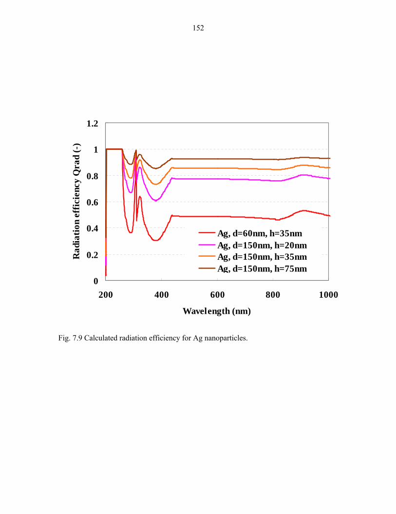
152
0
0.2
0.4
0.6
0.8
1
1.2
200 400 600 800 1000
Wavelength (nm)
Rad
iatio
n ef
ficie
ncy
Qra
d (-
)
Ag, d=60nm, h=35nmAg, d=150nm, h=20nmAg, d=150nm, h=35nmAg, d=150nm, h=75nm
Fig. 7.9 Calculated radiation efficiency for Ag nanoparticles.

153
0
10
20
30
40
50
60
70
80
90
200 400 600 800 1000
Wavelength (nm)
Qua
ntum
eff
icie
ncy
(%)
0
0.5
1
1.5
2
2.5
3
3.5
Nor
mal
ized
pho
tocu
rren
t (-)
w/o particlew/ Ag particles
0
10
20
30
40
50
60
70
80
90
200 400 600 800 1000
Wavelength (nm)
Qua
ntum
eff
icie
ncy
(%w/o particlew/ Ag particles
0
0.5
1
1.5
2
2.5
3
3.5
Nor
mal
ized
pho
tocu
rren
t (-))
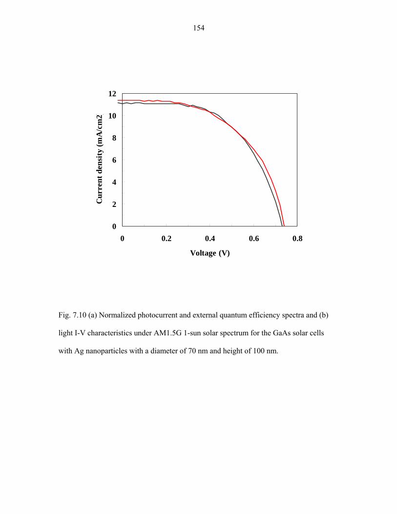
154
0
2
4
6
8
10
12
0 0.2 0.4 0.6 0.8
Voltage (V)
Cur
rent
den
sity
(mA
/cm
2)
Fig. 7.10 (a) Normalized photocurrent and external quantum efficiency spectra and (b)
light I-V characteristics under AM1.5G 1-sun solar spectrum for the GaAs solar cells
with Ag nanoparticles with a diameter of 70 nm and height of 100 nm.

155
50nm GaAs emitter (Zn 4x1018cm-3)50nm GaAs base (Si 2x1017cm-3)
30nm In0.49Ga0.51P window (Zn 1x1018cm-3)
30nm In0.49Ga0.51P BSF (Si 5x1018cm-3)
GaAsAu
Si substrate (B ~1x1019cm-3)
Au
Ag bondingAg reflection/bonding
Cr adhesion
Bondinterface
50nm GaAs emitter (Zn 4x1018cm-3)50nm GaAs base (Si 2x1017cm-3)
30nm In0.49Ga0.51P window (Zn 1x1018cm-3)
30nm In0.49Ga0.51P BSF (Si 5x1018cm-3)
GaAsAu
Si substrate (B ~1x1019cm-3)
Au
Ag bondingAg reflection/bonding
Cr adhesion
Bondinterface

156
50nm GaAs emitter (Zn 4x1018cm-3)50nm GaAs base (Si 2x1017cm-3)
1um GaAs buffer (Zn 2x1018cm-3)
GaAs substrate (Zn ~1x1018cm-3)
100nm In0.49Ga0.51P etch stop (no doped) 300nm GaAs contact (Zn 5x1018cm-3)
30nm In0.49Ga0.51P window (Zn 1x1018cm-3)
30nm In0.49Ga0.51P BSF (Si 5x1018cm-3)3um GaAs (Si 2x1018cm-3)
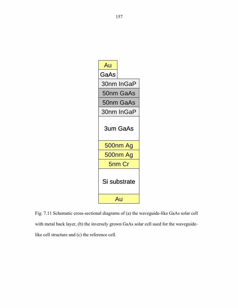
157
50nm GaAs50nm GaAs
30nm InGaP
30nm InGaP
GaAsAu
Si substrate
Au
500nm Ag500nm Ag
5nm Cr
3um GaAs
50nm GaAs50nm GaAs
30nm InGaP
30nm InGaP
GaAsAu
Si substrate
Au
500nm Ag500nm Ag
5nm Cr
3um GaAs
Fig. 7.11 Schematic cross-sectional diagrams of (a) the waveguide-like GaAs solar cell
with metal back layer, (b) the inversely grown GaAs solar cell used for the waveguide-
like cell structure and (c) the reference cell.
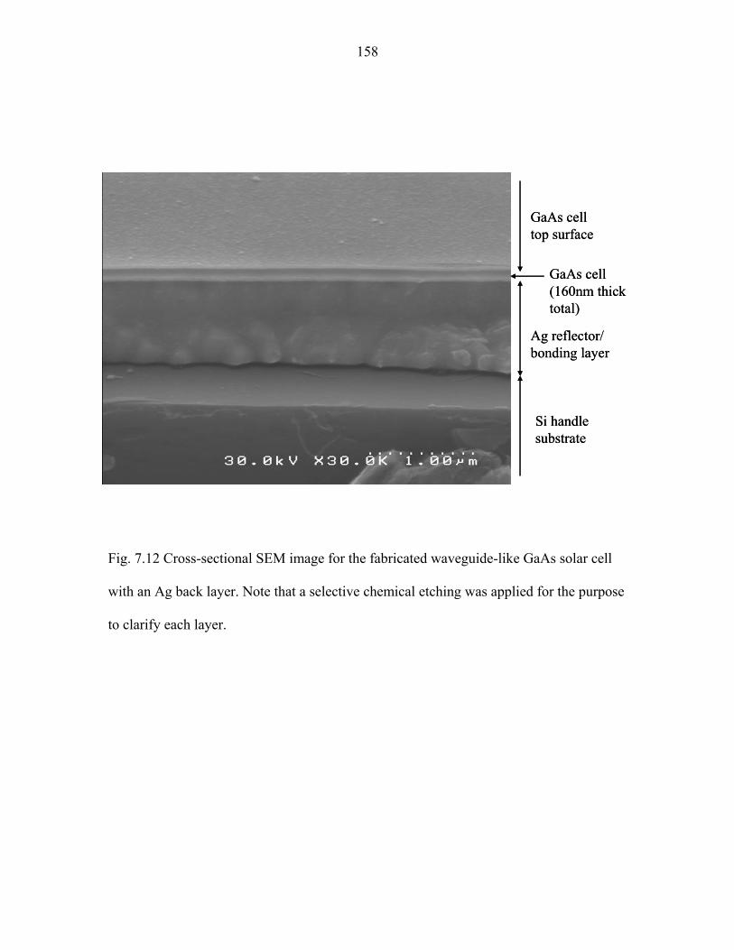
158
GaAs celltop surface
GaAs cell(160nm thicktotal)
Ag reflector/bonding layer
Si handlesubstrate
GaAs celltop surface
GaAs cell(160nm thicktotal)
Ag reflector/bonding layer
Si handlesubstrate
Fig. 7.12 Cross-sectional SEM image for the fabricated waveguide-like GaAs solar cell
with an Ag back layer. Note that a selective chemical etching was applied for the purpose
to clarify each layer.
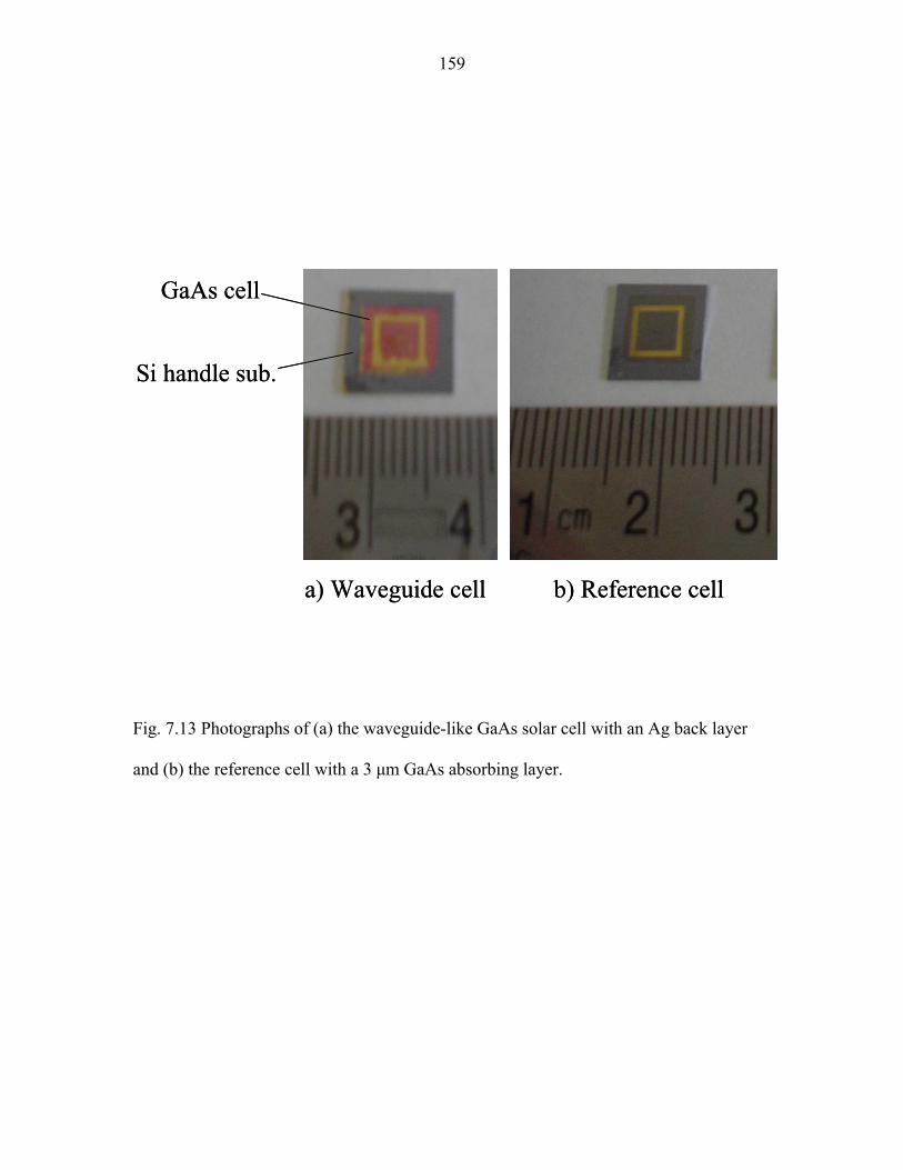
159
a) Waveguide cell b) Reference cell
GaAs cellGaAs cell
Fig. 7.13 Photographs of (a) the waveguide-like GaAs solar cell with an Ag back layer
and (b) the reference cell with a 3 μm GaAs absorbing layer.
Si handle sub.Si handle sub.
a) Waveguide cell b) Reference cell
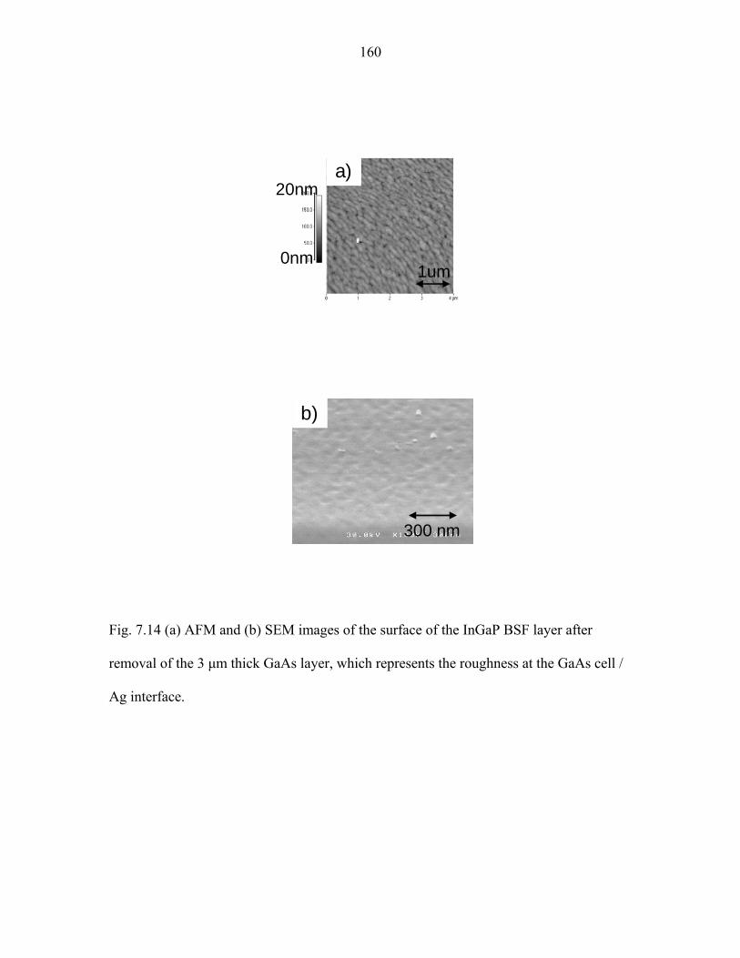
160
20nm
0nm1um
300 nm
b)
a)
Fig. 7.14 (a) AFM and (b) SEM images of the surface of the InGaP BSF layer after
removal of the 3 μm thick GaAs layer, which represents the roughness at the GaAs cell /
Ag interface.

161
0
2
4
6
8
10
12
14
0 0.2 0.4 0.6 0.8 1
Voltage (V)
Cur
rent
den
sity
(mA
/cm
2)WG cell 1WG cell 2WG cell 3Ref cell 1Ref cell 2
Fig. 7.15 Typical light I-V curves for the waveguide-like GaAs cells with Ag back
structure and the reference GaAs cells under AM1.5 Global solar spectrum with 1-sun
total intensity (100 mW cm-2).
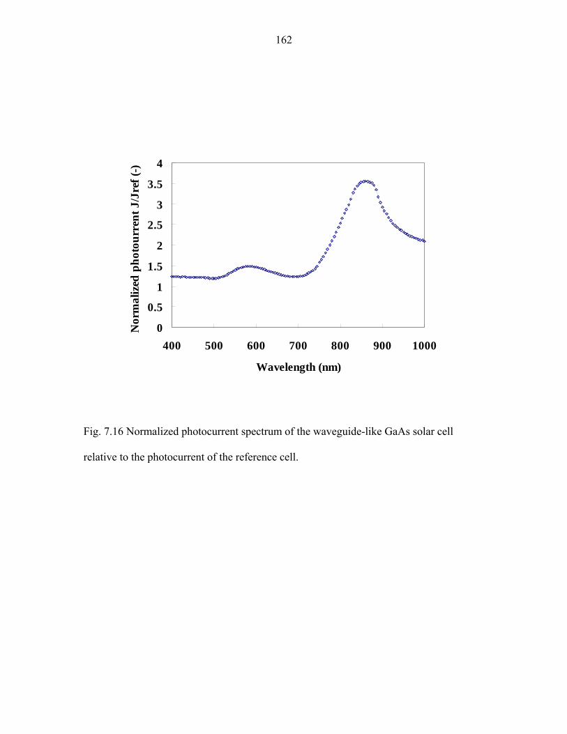
162
0
0.5
1
1.5
2
2.5
3
3.5
4
400 500 600 700 800 900 1000
Wavelength (nm)
Nor
mal
ized
pho
tour
rent
J/J
ref (
-)
Fig. 7.16 Normalized photocurrent spectrum of the waveguide-like GaAs solar cell
relative to the photocurrent of the reference cell.
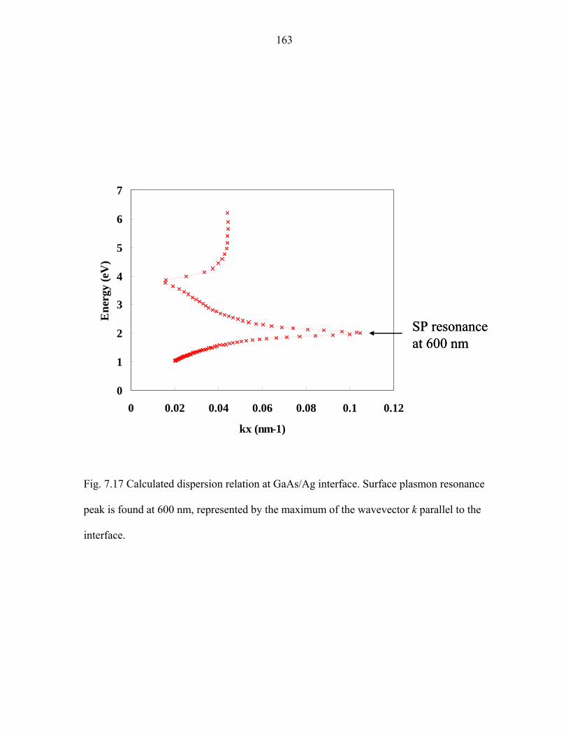
163
0
1
2
3
4
5
6
7
0 0.02 0.04 0.06 0.08 0.1 0.12
kx (nm-1)
Ene
rgy
(eV
)
SP resonanceat 600 nm
0
1
2
3
4
5
6
7
0 0.02 0.04 0.06 0.08 0.1 0.12
kx (nm-1)
Ene
rgy
(eV
)
SP resonanceat 600 nm
Fig. 7.17 Calculated dispersion relation at GaAs/Ag interface. Surface plasmon resonance
peak is found at 600 nm, represented by the maximum of the wavevector k parallel to the
interface.
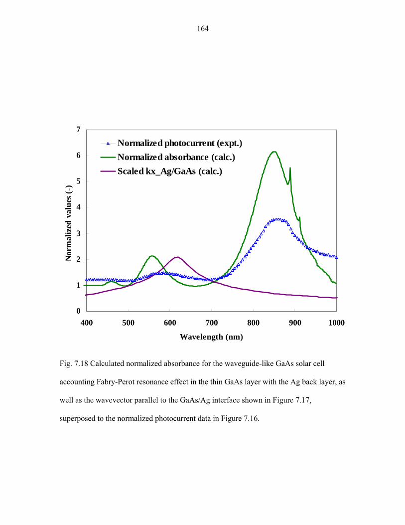
164
0
1
2
3
4
5
6
7
400 500 600 700 800 900 1000
Wavelength (nm)
Normalized photocurrent (expt.)Normalized absorbance (calc.)Scaled kx_Ag/GaAs (calc.)
rmze
dlu
(-)
es
va
ali
No
Fig. 7.18 Calculated normalized absorbance for the waveguide-like GaAs solar cell
accounting Fabry-Perot resonance effect in the thin GaAs layer with the Ag back layer, as
well as the wavevector parallel to the GaAs/Ag interface shown in Figure 7.17,
superposed to the normalized photocurrent data in Figure 7.16.

165
Chapter 8 Summary
In this thesis, I have investigated three major topics, wafer-bonded multijunction solar
cells, low cost alternative III-V-on-Si substrates and plasmonic solar cells. Wafer
bonding technologies were applied for all of these three projects. Lattice-matched
monolithic two-terminal GaAs/In0.53Ga0.47As dual-junction solar cells were fabricated
through GaAs/InP direct wafer bonding. InP/Si direct wafer bonding and also bonding
with a SiO2 bonding layer enabled high efficiency In0.53Ga0.47As solar cells on Si via
InP/Si alternative substrates. Ultrathin GaAs solar cells with Ag back structure were
prepared through wafer bonding of Ag-on-GaAs and Ag-on-Si wafers. I thus have
demonstrated various potential applications of wafer bonding with its excellent flexibility
for materials choice focusing on novel solar cell structures.
Low resistance Ohmic GaAs/InP junctions were obtained overcoming ~4% lattice
mismatch using direct wafer bonding technique. The key factors were reduction of the
interfacial oxygen and hydrogen by annealing in reduction atmosphere and high doping
for the interfacial bonding layers to induce tunneling current. The obtained bonded
GaAs/InP structures are suitable for lattice-mismatched multijunction solar cell
applications with their highly conductive interfaces. Simple considerations suggest that
for such a cell the currently-reported interfacial resistance smaller than 0.1 Ohm-cm2
would result in a negligible decrease in overall cell efficiency of ~0.02%, under 1-sun
illumination.
A direct-bond interconnected multijunction solar cell, a two-terminal monolithic
GaAs/InGaAs dual-junction cell, was then fabricated for the first time to demonstrate a

166
proof-of-principle for the viability of direct wafer bonding for solar cell applications. The
bonded interface is a metal-free n+GaAs/n+InP tunnel junction with highly conductive
Ohmic contact suitable for solar cell applications overcoming the 4% lattice mismatch.
The quantum efficiency spectrum for the bonded cell was quite similar to that for each of
unbonded GaAs and InGaAs subcells. The bonded dual-junction cell open-circuit voltage
was equal to the sum of the unbonded subcell open-circuit voltages, which indicates that
the bonding process does not degrade the cell material quality since any generated crystal
defects that act as recombination centers would reduce the open-circuit voltage. Also, the
bonded interface has no significant carrier recombination rate to reduce the open circuit
voltage.
Such a wafer bonding approach can also be applied to other photovoltaic
heterojunctions where lattice mismatch accommodation is also a challenge, such as the
(Al)InGaP/GaAs/InGaAsP/InGaAs four-junction tandem cell by bonding a GaAs-based
lattice-matched (Al)InGaP/GaAs subcell to an InP-based lattice-matched
InGaAsP/InGaAs subcell.
Low cost InP/Si alternative substrates were successfully fabricated by He implantation
of InP prior to bonding to a thermally oxidized Si substrate and annealing to exfoliate an
InP thin film. The thickness of the exfoliated InP films was only 900 nm, which means
hundreds of the InP/Si substrates could be prepared from a single InP wafer in principle.
The photovoltaic current-voltage characteristics of the In0.53Ga0.47As cells fabricated on
the wafer-bonded InP/Si substrates were comparable to those synthesized on
commercially available epi-ready InP substrates, and had a ~20% higher short-circuit

167
current which we attribute to the high reflectivity of the InP/SiO2/Si bonding interface.
This work provides an initial demonstration of wafer-bonded InP/Si substrates as an
alternative to bulk InP substrates for solar cell applications.
Ultimately, the InP/Si substrates are also extendable to fabrication of ultrahigh
efficiency four-junction (Al)InGaP/GaAs/InGaAsP/InGaAs cells via a direct bond
interconnect between subcell structures of InGaAsP/InGaAs grown on InP/Si and
(Al)InGaP/GaAs grown on GaAs to form the overall four junction cell structure.
Two types of “plasmonic” GaAs solar cell were investigated. Firstly, absorption
enhancement by metal nanoparticle scattering in ‘optically thin’ GaAs solar cells was
shown. Dense arrays of metal nanoparticles were deposited directly onto the Al0.8Ga0.2As
window layer of the GaAs cells through porous alumina membranes by thermal
evaporation. Spectral response measurements revealed photocurrent enhancements up to
260% at 900 nm for a GaAs cell with Ag nanoparticles with 150 nm diameter, 20 nm
height and 30% surface coverage, relative to reference GaAs cells with no metal
nanoparticle array. This photocurrent enhancement and the spectral behavior of the
normalized photocurrent are qualitatively reproduced by a simple optical model
representing surface plasmon resonance of metal nanoparticles and multi-angle scattering.
Particularly, larger subwavelength-size metal particles resulted in larger photocurrent due
to higher radiation efficiencies both for Ag and Al. Secondly, waveguide-like GaAs solar
cells with metallic back structures were introduced. Ultrathin GaAs cells with Ag back
layers were fabricated through wafer bonding and layer transfer with selective etch back
of the GaAs substrates. This waveguide-like GaAs cell showed net photocurrent

168
enhancement throughout the solar spectral range relative to the reference GaAs cell with
an absorbing GaAs back layer. A large peak for the normalized photocurrent around at
the GaAs bandedge was found and attributed to multiple-angle reflection at the Ag back
layer. A smaller peak was found at 600 nm and is due either to surface plasmon coupling
or Fabry-Perot resonance effect.
169
Appendix: Calculation codes
The calculations conducted in this Thesis were mostly all-analytical and therefore any
reader could straightforwardly reproduce the results. There however are a couple of
numerial calculations and I would like to explain them in this Appendix chapter.
The detailed balance limit efficiency calculation conducted in Chapter 2 contained only
one analytical calculation. Equation 10 is a transcendental equation about Vm and I used
the “Solver” function of Microsoft Excel to find the Vm which minimize the square of
(left hand - right hand).
For Equation 21 in Chapter 7, absorbance in multiple-angle scattering, the integration of
this equation cannot be solved analytically. I therefore conducted a numerical integration
with forward Euler method with a trapezoidal approximation using Visual Basic A, built
in Microsoft Excel. The code follows:
Sub integration_5()
'theta, s: angle
'alpha, a: absorption coefficient
'L: PV layer thickness
'F: absorbed fraction (the goal of this program)
'dF: part of F of that mesh (F = sum of dF's)

170
Dim s, ds, a(1000), L, F, dF As Double
L = [a7]
ds = ([a13] - [a10]) / [a16]
Dim i, i_final, j, j_final As Long
j = 0
j_final = [a19] - 4
Do
a(j) = Cells(j + 4, 15).Value
'In this macro, a(j) is actually the integrated alpha*L, not alpha.
i = 0
i_final = [a16] - 1
F = 0
s = [a10]
Do

171
If a(j) = 0 Then
dF = 0
ElseIf s > Cells(j + 4, 10).Value * 3.14159265358979 / 180 Then
dF = ds * 2 / 3 / 3.14159265358979 * (1 + (Cos(s)) ^ 2)
Else
'integration equation
'You can choose one of the two methods below.
'Trapezoidal method requires less meshes for convergence, but easier to overflow. (I don't
know why.)
'forward Euler
dF = ds * 2 / 3 / 3.14159265358979 * (1 + (Cos(s)) ^ 2) * (1 - Exp(-1 * a(j) / Cos(s)))
'considering one perfect reflection at the back surface
'trapezoidal
'dF = ds * (2 / 3 / 3.14159265358979 * (1 + (Cos(s)) ^ 2) * (1 - Exp(-a(j) * L / Cos(s))) +
2 / 3 / 3.14159265358979 * (1 + (Cos(s + ds)) ^ 2) * (1 - Exp(-a(j) * L / Cos(s + ds)))) / 2

172
'dF = ds * (1 / 3 / 3.14159265358979 * (1 + (Cos(s)) ^ 2) * (1 - Exp(-a(j) * L / Cos(s))) +
1 / 3 / 3.14159265358979 * (1 + (Cos(s + ds)) ^ 2) * (1 - Exp(-a(j) * L / Cos(s + ds))))
End If
F = F + dF
If i = i_final Then Exit Do
s = s + ds
i = i + 1
Loop
'output F into the cells on the worksheet
Cells(j + 4, 16) = F
If j = j_final Then Exit Do
j = j + 1
Loop
Beep
Beep

173
Beep
End Sub