Embed Size (px)
Citation preview

Summer 2017
Logistics Guide for Products Summer 2017
2 www.tfsemi.com Summer 2017©2017 TF Semicondutor Solutions (TFSS). All rights reserved. Information and data in this document are owned by TFSS and may not be edited, reproduced, or redistributed in any way without written consent from TFSS.
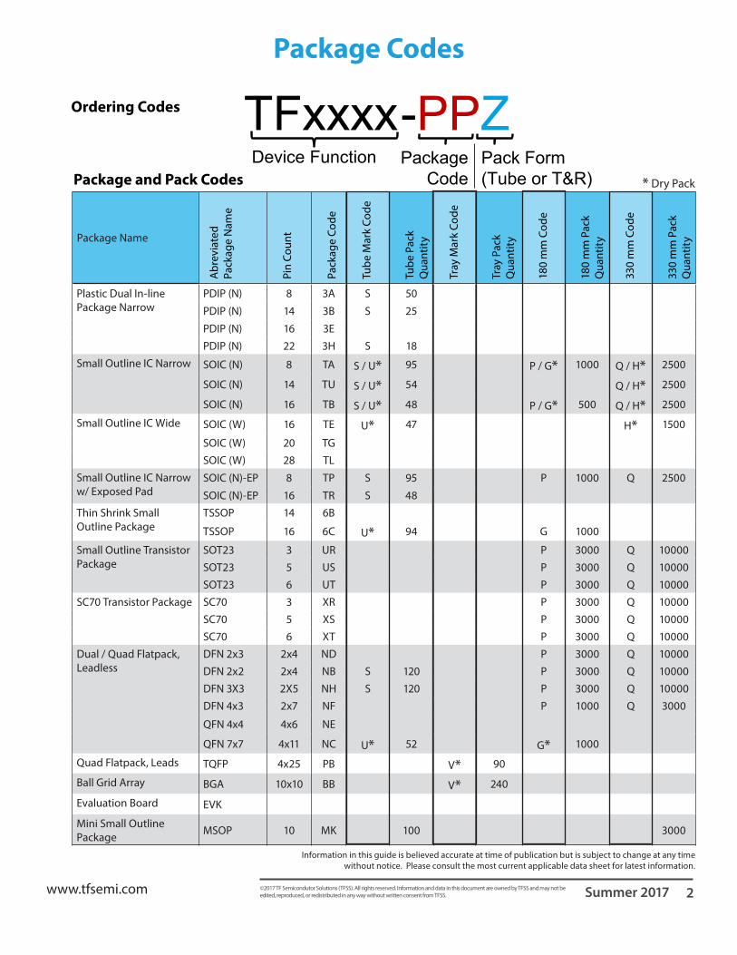
TFxxxx -PPZDevice Function Package
CodePack Form(Tube or T&R)Package and Pack Codes
Ordering Codes
Package Codes
Information in this guide is believed accurate at time of publication but is subject to change at any time without notice. Please consult the most current applicable data sheet for latest information.
Package Name
Abr
evia
ted
Pack
age
Nam
e
Pin
Coun
t
Pack
age
Code
Tube
Mar
k Co
de
Tube
Pac
k Q
uant
ity
Tray
Mar
k Co
de
Tray
Pac
k Q
uant
ity
180
mm
Cod
e
180
mm
Pac
k Q
uant
ity
330
mm
Cod
e
330
mm
Pac
k Q
uant
ity
Plastic Dual In-line Package Narrow
PDIP (N) 8 3A S 50
PDIP (N) 14 3B S 25
PDIP (N) 16 3E
PDIP (N) 22 3H S 18
Small Outline IC Narrow SOIC (N) 8 TA S / U* 95 P / G* 1000 Q / H* 2500
SOIC (N) 14 TU S / U* 54 Q / H* 2500
SOIC (N) 16 TB S / U* 48 P / G* 500 Q / H* 2500
Small Outline IC Wide SOIC (W) 16 TE U* 47 H* 1500
SOIC (W) 20 TG
SOIC (W) 28 TL
Small Outline IC Narrow w/ Exposed Pad
SOIC (N)-EP 8 TP S 95 P 1000 Q 2500
SOIC (N)-EP 16 TR S 48
Thin Shrink Small Outline Package
TSSOP 14 6B
TSSOP 16 6C U* 94 G 1000
Small Outline Transistor Package
SOT23 3 UR P 3000 Q 10000
SOT23 5 US P 3000 Q 10000
SOT23 6 UT P 3000 Q 10000
SC70 Transistor Package SC70 3 XR P 3000 Q 10000
SC70 5 XS P 3000 Q 10000
SC70 6 XT P 3000 Q 10000
Dual / Quad Flatpack, Leadless
DFN 2x3 2x4 ND P 3000 Q 10000
DFN 2x2 2x4 NB S 120 P 3000 Q 10000
DFN 3X3 2X5 NH S 120 P 3000 Q 10000
DFN 4x3 2x7 NF P 1000 Q 3000
QFN 4x4 4x6 NE
QFN 7x7 4x11 NC U* 52 G* 1000
Quad Flatpack, Leads TQFP 4x25 PB V* 90
Ball Grid Array BGA 10x10 BB V* 240
Evaluation Board EVK
Mini Small Outline Package MSOP 10 MK 100 3000
* Dry Pack

3 www.tfsemi.com Summer 2017©2017 TF Semicondutor Solutions (TFSS). All rights reserved. Information and data in this document are owned by TFSS and may not be edited, reproduced, or redistributed in any way without written consent from TFSS.
Package NameA
brev
iate
d Pa
ckag
e N
ame
Pin
Coun
t
Pack
age
Code
Lead
/ Ba
ll Pi
tch
(mm
)
Pack
age
Leng
th
L (m
m)
Pack
age
Wid
th
W (m
m)
Pack
age
Thic
knes
s T
(mm
)
Plastic Dual In-line Package Narrow
PDIP (N) 8 3A 2.54 9.80 6.30 3.60
PDIP (N) 14 3B 2.54 20.00 6.30 3.60
PDIP (N) 16 3E 2.54 20.00 6.30 3.60
PDIP (N) 22 3H 5.54 26.25 6.30 3.60
Small Outline IC Narrow SOIC (N) 8 TA 1.27 4.90 3.90 1.45
SOIC (N) 14 TU 1.27 3.90 1.45
SOIC (N) 16 TB 1.27 9.90 3.90 1.45
Small Outline IC Wide SOIC (W) 16 TE 1.27 10.30 7.47 2.50
SOIC (W) 20 TG 1.27 12.80 7.47 2.50
SOIC (W) 28 TL 1.00 18.30 8.40 3.00
Small Outline IC Narrow w/ Exposed Pad
SOIC (N)-EP 8 TP 1.27 4.90 3.90 1.45
SOIC (N)-EP 16 TR 1.27 9.90 3.90 1.45
Thin Shrink Small Outline Package
TSSOP 14 6B 0.65 5.00 4.40 0.90
TSSOP 16 6C 0.65 5.00 4.40 0.90
Small Outline Transistor Package
SOT23 3 UR 1.91 2.92 1.30 0.93
SOT23 5 US 0.95 2.92 1.60 1.02
SOT23 6 UT 0.95 2.92 1.60 1.02
SC70 Transistor Package SC70 3 XR 1.30 2.00 1.25 0.90
SC70 5 XS 0.65 2.00 1.25 0.90
SC70 6 XT 0.65 2.00 1.25 0.90
Dual / Quad Flatpack, Leadless
DFN 2x3 2x4 ND 0.50 2.00 1.25 0.90
DFN 2x2 2x4 NB 0.50 2.00 1.25 0.90
DFN 3x3 2X5 NH 0.50 2.00 2.00 0.75
DFN 4x3 2x7 NF 0.50 4.00 3.00 0.75
QFN 4x4 4x6 NE
QFN 7x7 4x11 NC 0.50 7.00 7.00 0.90
Quad Flatpack, Leads TQFP 4x25 PB 0.50 14.00 14.00 1.00
Ball Grid Array BGA 10x10 BB 0.80 10.00 10.00 1.40
Mini Small Outline Package MSOP 10 MK 0.50 4.90 3.00 1.10
TFxxxx -PPZDevice Function Package
CodePack Form(Tube or T&R)Package Dimensions
Package Dimensions
Information in this guide is believed accurate at time of publication but is subject to change at any time without notice. Please consult the most current applicable data sheet for latest information.
* Dry Pack
4 www.tfsemi.com Summer 2017©2017 TF Semicondutor Solutions (TFSS). All rights reserved. Information and data in this document are owned by TFSS and may not be edited, reproduced, or redistributed in any way without written consent from TFSS.
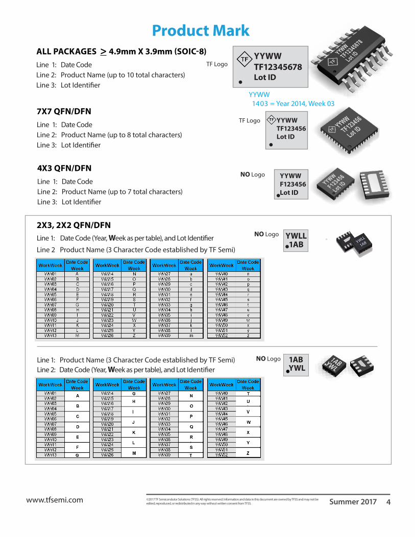
Product Mark
Line 1: Product Name (3 Character Code established by TF Semi)Line 2: Date Code (Year, Week as per table), and Lot Identifi er
ALL PACKAGES > 4.9mm X 3.9mm (SOIC-8) Line 1: Date Code Line 2: Product Name (up to 10 total characters)Line 3: Lot Identifi er
7X7 QFN/DFN Line 1: Date Code Line 2: Product Name (up to 8 total characters)Line 3: Lot Identifi er
YYWWTF12345678Lot ID
1ABYWL
YWLL1AB
4X3 QFN/DFN Line 1: Date Code Line 2: Product Name (up to 7 total characters)Line 3: Lot Identifi er
2X3, 2X2 QFN/DFNLine 1: Date Code (Year, Week as per table), and Lot Identifi er
Line 2 Product Name (3 Character Code established by TF Semi)
YYWWTF123456Lot ID
YYWWF123456Lot ID
TF Logo
NO Logo
NO Logo
NO Logo
TF Logo
YYWW 1403 = Year 2014, Week 03

5 www.tfsemi.com Summer 2017©2017 TF Semicondutor Solutions (TFSS). All rights reserved. Information and data in this document are owned by TFSS and may not be edited, reproduced, or redistributed in any way without written consent from TFSS.
Product Mark
SOT, SC70TOP: Product Name (3 Character Code established by TF Semi)
BOTTOM: Date Code (Year, Week as per table), and Lot Identifi er YWLL
1AB
Reference Table: Defi nition of single W format.
Y = Last digit of the yearW = Date Code Week
(see table)
L = Lot Identifi er
Information in this guide is believed accurate at time of publication but is subject to change at any time without notice. Please consult the most current applicable data sheet for latest information.
YWL1AB
Reference Table: Defi nition of single W format.
TOP: Product Name (3 Character Code established by TF Semi)
BOTTOM: Date Code (Year, Week as per table), and Lot Identifi er
Prior to date code 1X ( Dec 1st, 2011 )
TOP
BOTTOM
TOP
BOTTOM

6 www.tfsemi.com Summer 2017©2017 TF Semicondutor Solutions (TFSS). All rights reserved. Information and data in this document are owned by TFSS and may not be edited, reproduced, or redistributed in any way without written consent from TFSS.
Package Pin Count
SAP Code
Lead/Ball Pitch
(mm)
Package Length L
(mm)
Package Width W
(mm)
Package Thickness T
(mm)
TF Semi Devices (Ordering Code Examples)
PDIP (N) 8 3A 2.54 9.8 6.3 3.6TF2101-3AS, TF2103-3AS, TF2103A-3AS, TF2104-3AS, TF2104A-3AS, TF2190-3AS, TF2184-3AS, TF2117/2118-3AS, TF2106-3AS, TF2108-3AS, TF2181-3AS, TF1304-3AS
PDIP (N) 14 3B 2.54 20.0 6.3 3.6 TF2110-3BS, TF2113-3BS, TF21064-3BS, TF21084-3BS, TF21814-3BS, TF21844-3BS
PDIP (N) 16 3E 2.54 20.0 6.3 3.6PDIP (N) 18 3F 2.54 23.3 6.3 3.6PDIP (N) 20 3G 2.54 26.6 6.3 3.6
SOIC (N) 8 TA 1.27 4.9 3.9 1.45TF2101-TAU, TF2103-TAU, TF2103A-TAU, TF2104-TAU, TF2104A-TAU, TF2190-TAU, TF2184-TAU, TF2117/2118-TAU, TF2106-TAU, TF2108-TAU, TF2181-TAU, TF1304-TAU, TF6001-TAU, TF6002-TAU, TF1503-TAU, TF1504-TAU
SOIC (N) 14 TU 1.27 8.64 3.9 1.45 TF21064-TUU, TF21084-TUU, TF21814-TUU, TF21844-TUU
SOIC (N) 16 TB 1.27 9.91 3.9 1.45
SOIC (W) 16 TE 1.27 10.3 7.47 2.5 TF2110-TEU, TF2113-TEU
SOIC (W) 20 TG 1.27 12.8 7.47 2.5
SOIC (W) 28 TL 1.27 18.0 7.47 2.5 TF23892-TLU, TF1692-TLU, TF0692-TLU, TF2136-TLU, TF1636-TLU, TF0636-TLU
SOIC (N)-EP 8 TP 1.27 4.90 3.9 1.45 TF6003-TPU
SOIC (N)-EP 16 TR 1.27 9.91 3.9 1.45
TSSOP 14 6B 0.65 5.0 4.4 0.9
TSSOP 16 6C 0.65 5.0 4.4 0.9 TF90LVDS047-6CU, TF90LVDS048-6CU
SOT23 3 UR 1.91 2.92 1.3 0.93
SOT23 5 US 0.95 2.92 1.6 1.02
SOT23 6 UT 0.95 2.92 1.6 1.02 TF4601A-UT45U, TF4601B-UT20U, TF4602-UT28U
SC70 3 XR 1.3 2.0 1.25 0.9
SC70 5 XS 0.65 2.0 1.25 0.9
SC70 6 XT 0.65 2.0 1.25 0.9
QFN 4x2 NA 0.5 2.0 2.0 0.9
QFN 2x4 NB 0.5 2.0 2.0 0.9 TF4601A-NB45U, TF4601B-NB20U
TDFN 2x5 NH 0.5 3.0 3.0 0.75 TF0503-NHS, TF0504-NHS, TF0506-NHS, TF0507-NHS
TQFP 4x16 PA 0.5 10.0 10.0 1.0
TQFP 4x25 PB 0.5 14.0 14.0 1.0 TF112-PBU
BGA 8x8 BA 0.80 8.0 8.0 1.4
BGA 10x10 BB 0.80 10.0 10.0 1.4 TF112-BBU
Package Reference Data
www.tfsemi.com
[email protected] +(1) 877-924-5001 NORTH AMERICA
7501 Foothills Blvd, Roseville, CA 95747, USA Tel: +(1) 877-924-5001
ASIA Rm. 607, Bldg. 4, 1st Phase Software Park, 2nd Keji Middle Road, Hi-Tech
Park, Nanshan District, Shenzhen City, 518052, PRC Tel: + 86-1351-102-3160
7Spring 2017©2017 TF Semicondutor Solutions (TFSS). All rights reserved. Information and data in this document are owned by TFSS and may not be edited, reproduced, or redistributed in any way without written consent from TFSS.
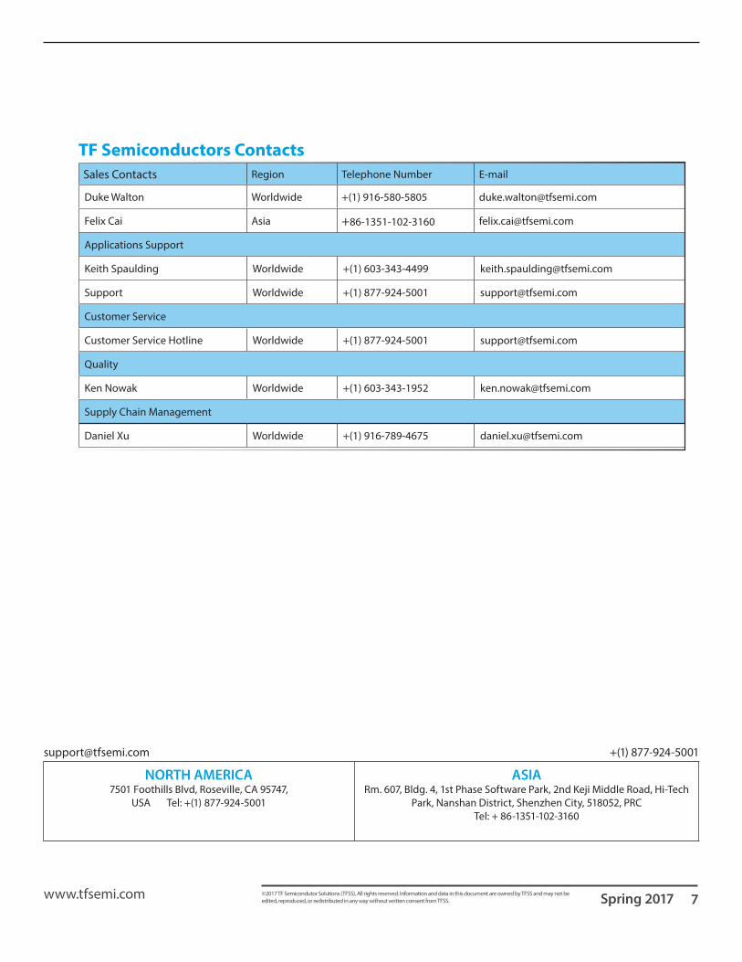
Sales Contacts Region Telephone Number E-mail
Duke Walton Worldwide +(1) 916-580-5805 [email protected]
Felix Cai Asia +86-1351-102-3160 [email protected]
Applications Support
Keith Spaulding Worldwide +(1) 603-343-4499 [email protected]
Support Worldwide +(1) 877-924-5001 [email protected]
Customer Service
Customer Service Hotline Worldwide +(1) 877-924-5001 [email protected]
Quality
Ken Nowak Worldwide +(1) 603-343-1952 [email protected]
Supply Chain Management
Daniel Xu Worldwide +(1) 916-789-4675 [email protected]
TF Semiconductors Contacts

8 www.tfsemi.com Summer 2017©2017 TF Semicondutor Solutions (TFSS). All rights reserved. Information and data in this document are owned by TFSS and may not be edited, reproduced, or redistributed in any way without written consent from TFSS.
TF Semiconductor Solutions (TFSS) PRODUCTS ARE NEITHER DESIGNED NOR INTENDED FOR USE IN MILITARY AND/OR AEROSPACE, AUTOMOTIVE OR MEDICAL DEVICES OR SYSTEMS UNLESS THE SPECIFIC TFSS PRODUCTS ARE SPECIFICALLY DESIGNATED BY TFSS FOR SUCH USE. BUYERS ACKNOWLEDGE AND AGREE THAT ANY SUCH USE OF TFSS PRODUCTS WHICH TFSS HAS NOT DESIGNATED FOR USE IN MILITARY AND/OR AEROSPACE, AUTOMOTIVE OR MEDICAL DEVICES OR SYSTEMS IS SOLELY AT THE BUYER’S RISK.
TFSS assumes no liability for application assistance or customer product design. Customers are responsible for their products and applications using TFSS products.
Resale of TFSS products or services with statements different from or beyond the parameters stated by TFSS for that product or service voids all express and any implied warranties for the associated TFSS product or service. TFSS is not responsible or liable for any such statements.
©2017 TFSS. All Rights Reserved. Information and data in this document are owned by TFSS wholly and may not be edited, reproduced, or redistributed in any way without the express written consent from TFSS.
Important Notice


![QUANTUM DOTS- SMART SEMICONDUTOR …Nanotechnology is the engineering of functional system at the molecular scale[1]. It is the art and science of ... March 27th, 2012. . “ ”,](https://img.pdfslide.us/doc/110x75/5f21889ddf71f46be46b6986/quantum-dots-smart-semicondutor-nanotechnology-is-the-engineering-of-functional.jpg)