Embed Size (px)
Citation preview
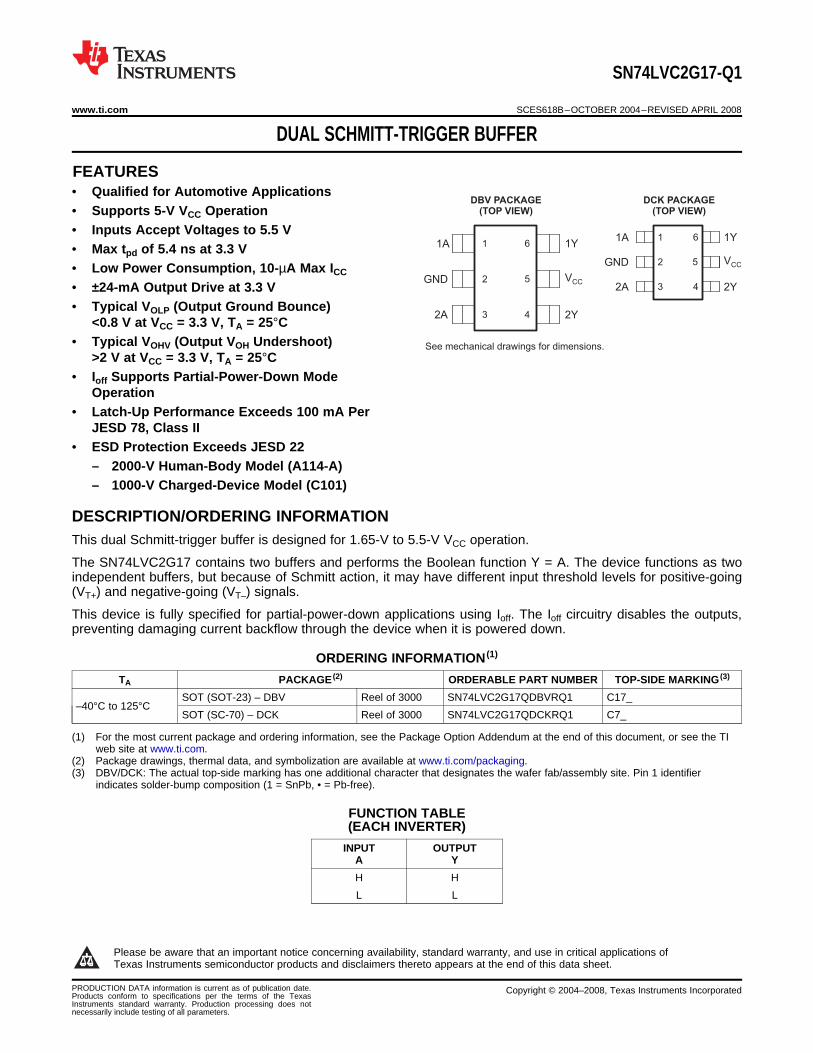
1FEATURES
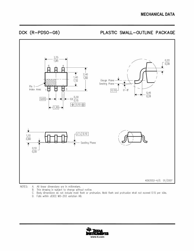
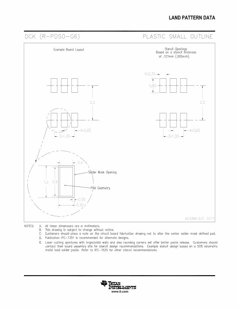
See mechanical drawings for dimensions.
DBV PACKAGE(TOP VIEW)
DCK PACKAGE(TOP VIEW)
2GND VCC5
3 42A 2Y
611A 1Y
3 42A
2GND
2Y
5
11A
VCC
6 1Y
DESCRIPTION/ORDERING INFORMATION
SN74LVC2G17-Q1
www.ti.com .................................................................................................................................................... SCES618B–OCTOBER 2004–REVISED APRIL 2008
DUAL SCHMITT-TRIGGER BUFFER
• Qualified for Automotive Applications• Supports 5-V VCC Operation• Inputs Accept Voltages to 5.5 V• Max tpd of 5.4 ns at 3.3 V• Low Power Consumption, 10-µA Max ICC
• ±24-mA Output Drive at 3.3 V• Typical VOLP (Output Ground Bounce)
<0.8 V at VCC = 3.3 V, TA = 25°C• Typical VOHV (Output VOH Undershoot)
>2 V at VCC = 3.3 V, TA = 25°C• Ioff Supports Partial-Power-Down Mode
Operation• Latch-Up Performance Exceeds 100 mA Per
JESD 78, Class II• ESD Protection Exceeds JESD 22
– 2000-V Human-Body Model (A114-A)– 1000-V Charged-Device Model (C101)
This dual Schmitt-trigger buffer is designed for 1.65-V to 5.5-V VCC operation.
The SN74LVC2G17 contains two buffers and performs the Boolean function Y = A. The device functions as twoindependent buffers, but because of Schmitt action, it may have different input threshold levels for positive-going(VT+) and negative-going (VT–) signals.
This device is fully specified for partial-power-down applications using Ioff. The Ioff circuitry disables the outputs,preventing damaging current backflow through the device when it is powered down.
ORDERING INFORMATION (1)
TA PACKAGE (2) ORDERABLE PART NUMBER TOP-SIDE MARKING (3)
SOT (SOT-23) – DBV Reel of 3000 SN74LVC2G17QDBVRQ1 C17_–40°C to 125°C
SOT (SC-70) – DCK Reel of 3000 SN74LVC2G17QDCKRQ1 C7_
(1) For the most current package and ordering information, see the Package Option Addendum at the end of this document, or see the TIweb site at www.ti.com.
(2) Package drawings, thermal data, and symbolization are available at www.ti.com/packaging.(3) DBV/DCK: The actual top-side marking has one additional character that designates the wafer fab/assembly site. Pin 1 identifier
indicates solder-bump composition (1 = SnPb, • = Pb-free).
FUNCTION TABLE(EACH INVERTER)
INPUT OUTPUTA YH HL L
1
Please be aware that an important notice concerning availability, standard warranty, and use in critical applications ofTexas Instruments semiconductor products and disclaimers thereto appears at the end of this data sheet.
PRODUCTION DATA information is current as of publication date. Copyright © 2004–2008, Texas Instruments IncorporatedProducts conform to specifications per the terms of the TexasInstruments standard warranty. Production processing does notnecessarily include testing of all parameters.
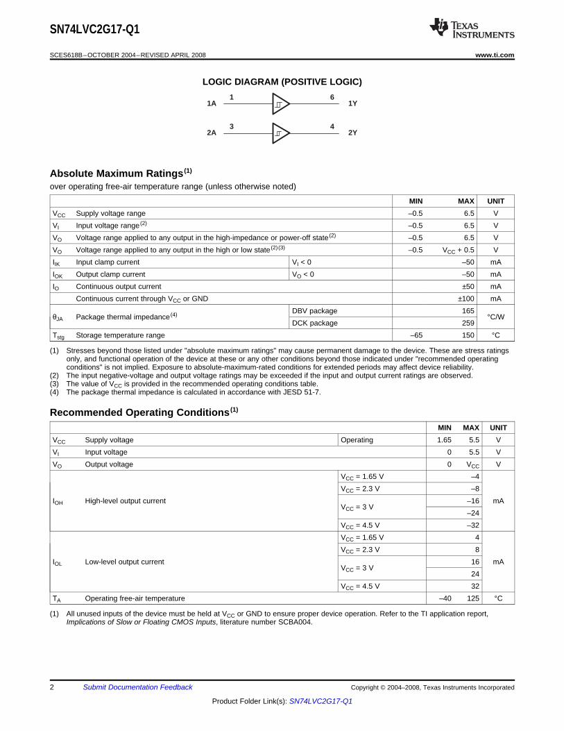
1A 1Y1 6
2A 2Y3 4
Absolute Maximum Ratings (1)
Recommended Operating Conditions (1)
SN74LVC2G17-Q1
SCES618B–OCTOBER 2004–REVISED APRIL 2008.................................................................................................................................................... www.ti.com
LOGIC DIAGRAM (POSITIVE LOGIC)
over operating free-air temperature range (unless otherwise noted)
MIN MAX UNITVCC Supply voltage range –0.5 6.5 VVI Input voltage range (2) –0.5 6.5 VVO Voltage range applied to any output in the high-impedance or power-off state (2) –0.5 6.5 VVO Voltage range applied to any output in the high or low state (2) (3) –0.5 VCC + 0.5 VIIK Input clamp current VI < 0 –50 mAIOK Output clamp current VO < 0 –50 mAIO Continuous output current ±50 mA
Continuous current through VCC or GND ±100 mADBV package 165
θJA Package thermal impedance (4) °C/WDCK package 259
Tstg Storage temperature range –65 150 °C
(1) Stresses beyond those listed under "absolute maximum ratings" may cause permanent damage to the device. These are stress ratingsonly, and functional operation of the device at these or any other conditions beyond those indicated under "recommended operatingconditions" is not implied. Exposure to absolute-maximum-rated conditions for extended periods may affect device reliability.
(2) The input negative-voltage and output voltage ratings may be exceeded if the input and output current ratings are observed.(3) The value of VCC is provided in the recommended operating conditions table.(4) The package thermal impedance is calculated in accordance with JESD 51-7.
MIN MAX UNITVCC Supply voltage Operating 1.65 5.5 VVI Input voltage 0 5.5 VVO Output voltage 0 VCC V
VCC = 1.65 V –4VCC = 2.3 V –8
IOH High-level output current –16 mAVCC = 3 V
–24VCC = 4.5 V –32VCC = 1.65 V 4VCC = 2.3 V 8
IOL Low-level output current 16 mAVCC = 3 V
24VCC = 4.5 V 32
TA Operating free-air temperature –40 125 °C
(1) All unused inputs of the device must be held at VCC or GND to ensure proper device operation. Refer to the TI application report,Implications of Slow or Floating CMOS Inputs, literature number SCBA004.
2 Submit Documentation Feedback Copyright © 2004–2008, Texas Instruments Incorporated
Product Folder Link(s): SN74LVC2G17-Q1
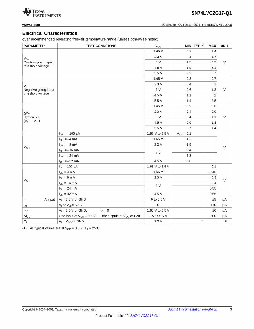
Electrical Characteristics
SN74LVC2G17-Q1
www.ti.com .................................................................................................................................................... SCES618B–OCTOBER 2004–REVISED APRIL 2008
over recommended operating free-air temperature range (unless otherwise noted)
PARAMETER TEST CONDITIONS VCC MIN TYP (1) MAX UNIT1.65 V 0.7 1.42.3 V 1 1.7VT+
Positive-going input 3 V 1.3 2.2 Vthreshold voltage 4.5 V 1.9 3.1
5.5 V 2.2 3.71.65 V 0.3 0.72.3 V 0.4 1VT–
Negative-going input 3 V 0.6 1.3 Vthreshold voltage 4.5 V 1.1 2
5.5 V 1.4 2.51.65 V 0.3 0.82.3 V 0.4 0.9ΔVT
Hysteresis 3 V 0.4 1.1 V(VT+ – VT–) 4.5 V 0.6 1.3
5.5 V 0.7 1.4IOH = –100 µA 1.65 V to 5.5 V VCC – 0.1IOH = –4 mA 1.65 V 1.2IOH = –8 mA 2.3 V 1.9
VOH VIOH = –16 mA 2.4
3 VIOH = –24 mA 2.3IOH = –32 mA 4.5 V 3.8IOL = 100 µA 1.65 V to 5.5 V 0.1IOL = 4 mA 1.65 V 0.45IOL = 8 mA 2.3 V 0.3
VOL VIOL = 16 mA 0.4
3 VIOL = 24 mA 0.55IOL = 32 mA 4.5 V 0.55
II A input VI = 5.5 V or GND 0 to 5.5 V ±5 µAIoff VI or VO = 5.5 V 0 ±10 µAICC VI = 5.5 V or GND, IO = 0 1.65 V to 5.5 V 10 µAΔICC One input at VCC – 0.6 V, Other inputs at VCC or GND 3 V to 5.5 V 500 µACi VI = VCC or GND 3.3 V 4 pF
(1) All typical values are at VCC = 3.3 V, TA = 25°C.
Copyright © 2004–2008, Texas Instruments Incorporated Submit Documentation Feedback 3
Product Folder Link(s): SN74LVC2G17-Q1
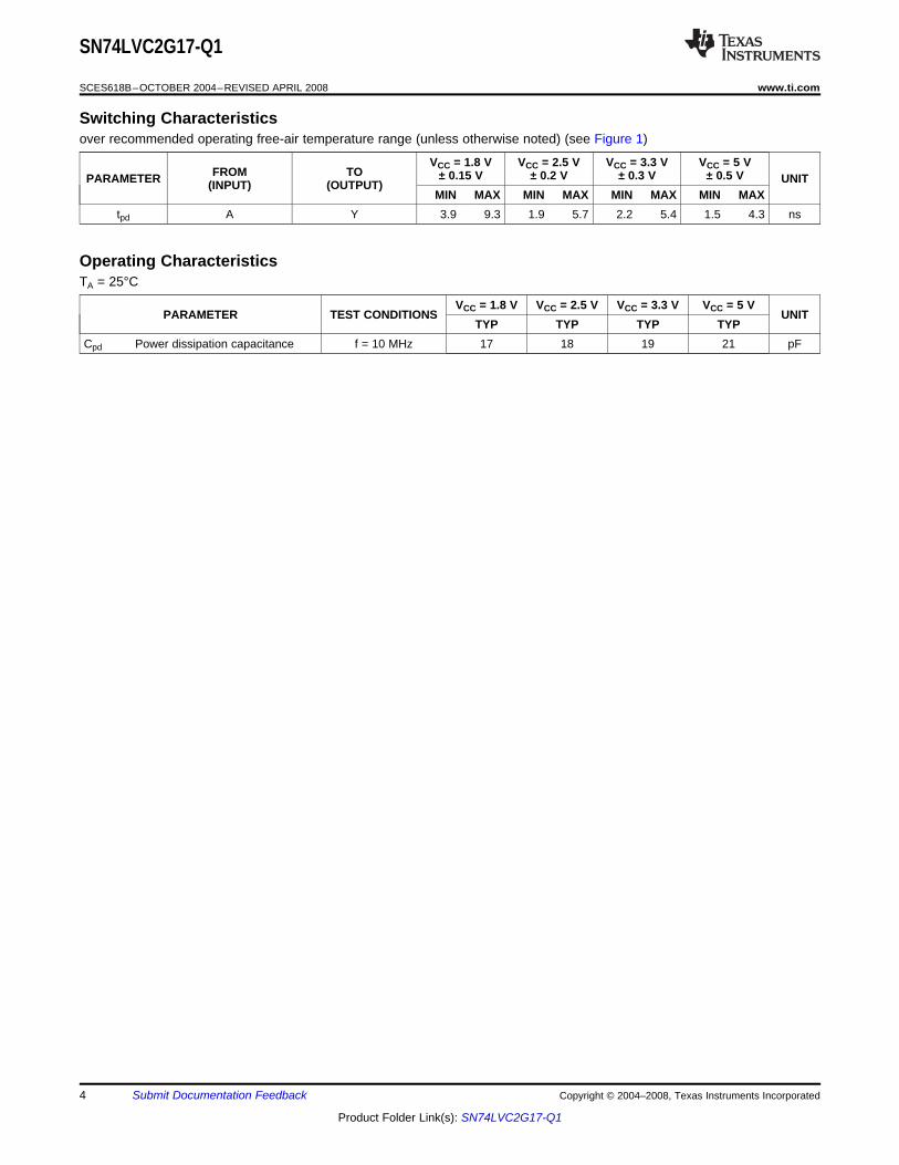
Switching Characteristics
Operating Characteristics
SN74LVC2G17-Q1
SCES618B–OCTOBER 2004–REVISED APRIL 2008.................................................................................................................................................... www.ti.com
over recommended operating free-air temperature range (unless otherwise noted) (see Figure 1)
VCC = 1.8 V VCC = 2.5 V VCC = 3.3 V VCC = 5 VFROM TO ± 0.15 V ± 0.2 V ± 0.3 V ± 0.5 VPARAMETER UNIT(INPUT) (OUTPUT)
MIN MAX MIN MAX MIN MAX MIN MAXtpd A Y 3.9 9.3 1.9 5.7 2.2 5.4 1.5 4.3 ns
TA = 25°C
VCC = 1.8 V VCC = 2.5 V VCC = 3.3 V VCC = 5 VPARAMETER TEST CONDITIONS UNIT
TYP TYP TYP TYPCpd Power dissipation capacitance f = 10 MHz 17 18 19 21 pF
4 Submit Documentation Feedback Copyright © 2004–2008, Texas Instruments Incorporated
Product Folder Link(s): SN74LVC2G17-Q1
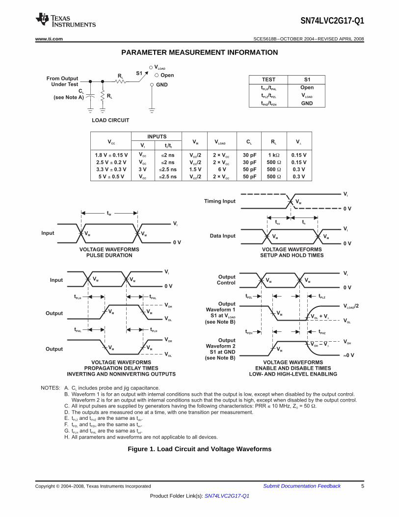
PARAMETER MEASUREMENT INFORMATION
thtsu
From OutputUnder Test
C
(see Note A)L
LOAD CIRCUIT
S1
VLOAD
Open
GND
RL
Data Input
Timing Input
0 V
0 V0 V
tW
Input
0 VInput
OutputWaveform 1
S1 at V
(see Note B)LOAD
OutputWaveform 2
S1 at GND(see Note B)
VOL
VOH
0 V
»0 V
Output
Output
TEST S1
t /tPLH PHL Open
OutputControl
VM
VM VM
VM
VM
1.8 V 0.15 V±
2.5 V 0.2 V±
3.3 V 0.3 V±
5 V 0.5 V±
1 kW
500 W
500 W
500 W
VCC RL
2 × VCC
2 × VCC
6 V
2 × VCC
VLOAD CL
30 pF
30 pF
50 pF
50 pF
0.15 V
0.15 V
0.3 V
0.3 V
VD
3 V
VI
VCC/2
VCC/2
1.5 V
VCC/2
VM
£2 ns
£2 ns
£2.5 ns
£2.5 ns
INPUTS
RL
t /tr f
VCC
VCC
VCC
VLOADt /tPLZ PZL
GNDt /tPHZ PZH
VOLTAGE WAVEFORMSENABLE AND DISABLE TIMES
LOW- AND HIGH-LEVEL ENABLING
VOLTAGE WAVEFORMSPROPAGATION DELAY TIMES
INVERTING AND NONINVERTING OUTPUTS
NOTES: A. C includes probe and jig capacitance.
B. Waveform 1 is for an output with internal conditions such that the output is low, except when disabled by the output control.Waveform 2 is for an output with internal conditions such that the output is high, except when disabled by the output control.
C. All input pulses are supplied by generators having the following characteristics: PRR 10 MHz, Z = 50 .
D. The outputs are measured one at a time, with one transition per measurement.E. t and t are the same as t .
F. t and t are the same as t .
G. t and t are the same as t .
H. All parameters and waveforms are not applicable to all devices.
L
O
PLZ PHZ dis
PZL PZH en
PLH PHL pd
£ W
VOLTAGE WAVEFORMSPULSE DURATION
VOLTAGE WAVEFORMSSETUP AND HOLD TIMES
VI
VI
VI
VM
VM
V /2LOAD
tPZL tPLZ
tPHZtPZH
V – VOH D
V + VOL D
VM
VM VM
VM
VOL
VOH
VI
VI
VOH
VOL
VM
VM
VM
VM
tPLH tPHL
tPLHtPHL
SN74LVC2G17-Q1
www.ti.com .................................................................................................................................................... SCES618B–OCTOBER 2004–REVISED APRIL 2008
Figure 1. Load Circuit and Voltage Waveforms
Copyright © 2004–2008, Texas Instruments Incorporated Submit Documentation Feedback 5
Product Folder Link(s): SN74LVC2G17-Q1
PACKAGE OPTION ADDENDUM
www.ti.com 10-Dec-2020
Addendum-Page 1
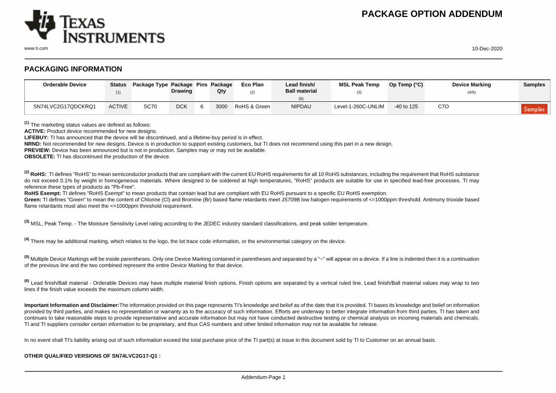
PACKAGING INFORMATION
Orderable Device Status(1)
Package Type PackageDrawing
Pins PackageQty
Eco Plan(2)
Lead finish/Ball material
(6)
MSL Peak Temp(3)
Op Temp (°C) Device Marking(4/5)
Samples
SN74LVC2G17QDCKRQ1 ACTIVE SC70 DCK 6 3000 RoHS & Green NIPDAU Level-1-260C-UNLIM -40 to 125 C7O
(1) The marketing status values are defined as follows:ACTIVE: Product device recommended for new designs.LIFEBUY: TI has announced that the device will be discontinued, and a lifetime-buy period is in effect.NRND: Not recommended for new designs. Device is in production to support existing customers, but TI does not recommend using this part in a new design.PREVIEW: Device has been announced but is not in production. Samples may or may not be available.OBSOLETE: TI has discontinued the production of the device.
(2) RoHS: TI defines "RoHS" to mean semiconductor products that are compliant with the current EU RoHS requirements for all 10 RoHS substances, including the requirement that RoHS substancedo not exceed 0.1% by weight in homogeneous materials. Where designed to be soldered at high temperatures, "RoHS" products are suitable for use in specified lead-free processes. TI mayreference these types of products as "Pb-Free".RoHS Exempt: TI defines "RoHS Exempt" to mean products that contain lead but are compliant with EU RoHS pursuant to a specific EU RoHS exemption.Green: TI defines "Green" to mean the content of Chlorine (Cl) and Bromine (Br) based flame retardants meet JS709B low halogen requirements of <=1000ppm threshold. Antimony trioxide basedflame retardants must also meet the <=1000ppm threshold requirement.
(3) MSL, Peak Temp. - The Moisture Sensitivity Level rating according to the JEDEC industry standard classifications, and peak solder temperature.
(4) There may be additional marking, which relates to the logo, the lot trace code information, or the environmental category on the device.
(5) Multiple Device Markings will be inside parentheses. Only one Device Marking contained in parentheses and separated by a "~" will appear on a device. If a line is indented then it is a continuationof the previous line and the two combined represent the entire Device Marking for that device.
(6) Lead finish/Ball material - Orderable Devices may have multiple material finish options. Finish options are separated by a vertical ruled line. Lead finish/Ball material values may wrap to twolines if the finish value exceeds the maximum column width.
Important Information and Disclaimer:The information provided on this page represents TI's knowledge and belief as of the date that it is provided. TI bases its knowledge and belief on informationprovided by third parties, and makes no representation or warranty as to the accuracy of such information. Efforts are underway to better integrate information from third parties. TI has taken andcontinues to take reasonable steps to provide representative and accurate information but may not have conducted destructive testing or chemical analysis on incoming materials and chemicals.TI and TI suppliers consider certain information to be proprietary, and thus CAS numbers and other limited information may not be available for release.
In no event shall TI's liability arising out of such information exceed the total purchase price of the TI part(s) at issue in this document sold by TI to Customer on an annual basis.
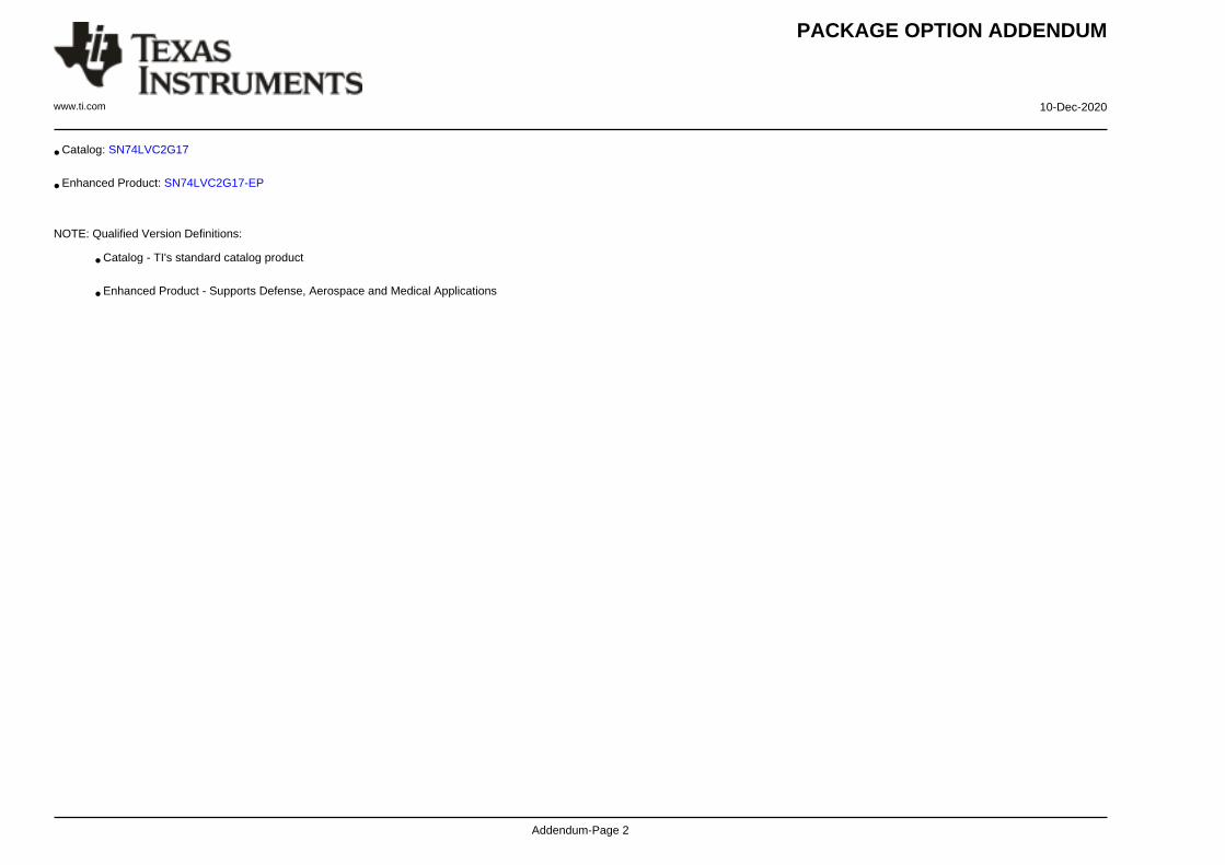
OTHER QUALIFIED VERSIONS OF SN74LVC2G17-Q1 :
PACKAGE OPTION ADDENDUM
www.ti.com 10-Dec-2020
Addendum-Page 2
• Catalog: SN74LVC2G17
• Enhanced Product: SN74LVC2G17-EP
NOTE: Qualified Version Definitions:
• Catalog - TI's standard catalog product
• Enhanced Product - Supports Defense, Aerospace and Medical Applications
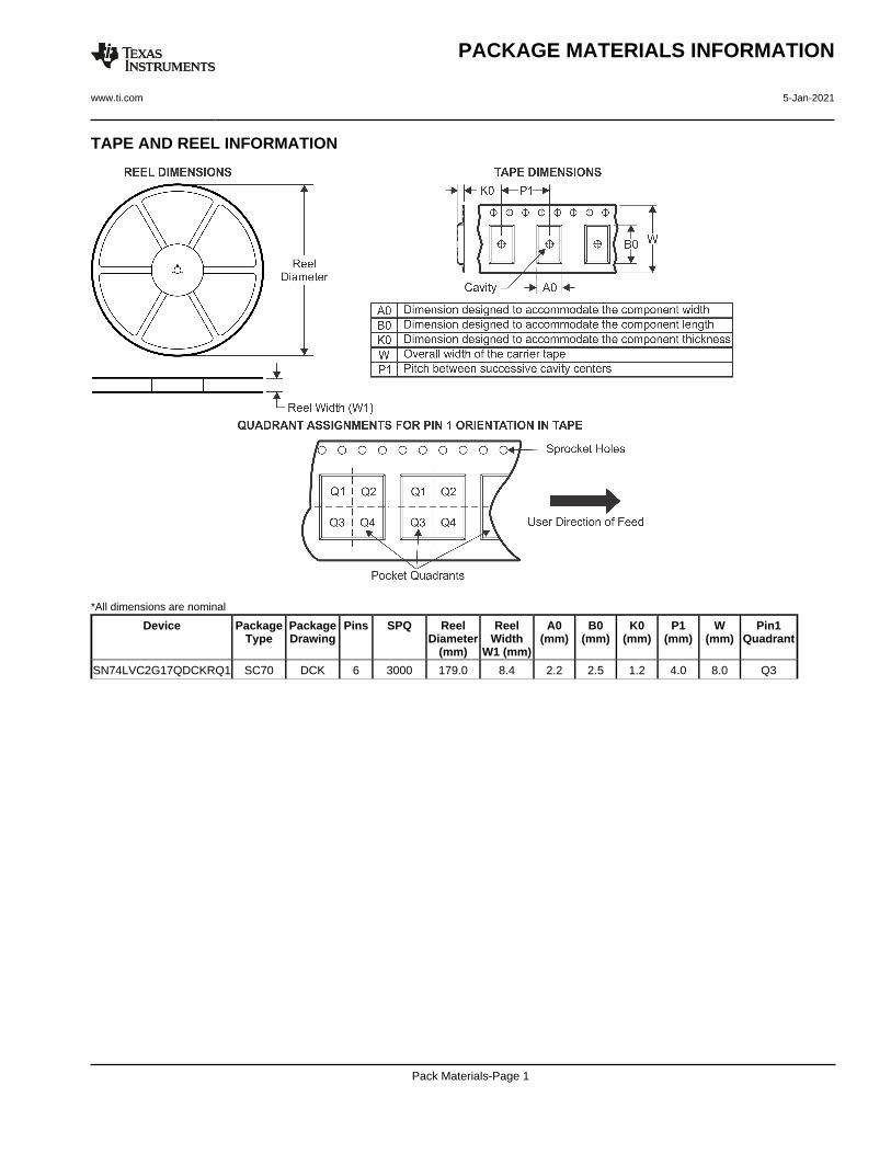
TAPE AND REEL INFORMATION
*All dimensions are nominal
Device PackageType
PackageDrawing
Pins SPQ ReelDiameter
(mm)
ReelWidth
W1 (mm)
A0(mm)
B0(mm)
K0(mm)
P1(mm)
W(mm)
Pin1Quadrant
SN74LVC2G17QDCKRQ1 SC70 DCK 6 3000 179.0 8.4 2.2 2.5 1.2 4.0 8.0 Q3
PACKAGE MATERIALS INFORMATION
www.ti.com 5-Jan-2021
Pack Materials-Page 1
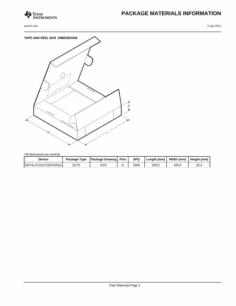
*All dimensions are nominal
Device Package Type Package Drawing Pins SPQ Length (mm) Width (mm) Height (mm)
SN74LVC2G17QDCKRQ1 SC70 DCK 6 3000 200.0 183.0 25.0
PACKAGE MATERIALS INFORMATION
www.ti.com 5-Jan-2021
Pack Materials-Page 2
IMPORTANT NOTICE AND DISCLAIMERTI PROVIDES TECHNICAL AND RELIABILITY DATA (INCLUDING DATASHEETS), DESIGN RESOURCES (INCLUDING REFERENCEDESIGNS), APPLICATION OR OTHER DESIGN ADVICE, WEB TOOLS, SAFETY INFORMATION, AND OTHER RESOURCES “AS IS”AND WITH ALL FAULTS, AND DISCLAIMS ALL WARRANTIES, EXPRESS AND IMPLIED, INCLUDING WITHOUT LIMITATION ANYIMPLIED WARRANTIES OF MERCHANTABILITY, FITNESS FOR A PARTICULAR PURPOSE OR NON-INFRINGEMENT OF THIRDPARTY INTELLECTUAL PROPERTY RIGHTS.These resources are intended for skilled developers designing with TI products. You are solely responsible for (1) selecting the appropriateTI products for your application, (2) designing, validating and testing your application, and (3) ensuring your application meets applicablestandards, and any other safety, security, or other requirements. These resources are subject to change without notice. TI grants youpermission to use these resources only for development of an application that uses the TI products described in the resource. Otherreproduction and display of these resources is prohibited. No license is granted to any other TI intellectual property right or to any third partyintellectual property right. TI disclaims responsibility for, and you will fully indemnify TI and its representatives against, any claims, damages,costs, losses, and liabilities arising out of your use of these resources.TI’s products are provided subject to TI’s Terms of Sale (https:www.ti.com/legal/termsofsale.html) or other applicable terms available eitheron ti.com or provided in conjunction with such TI products. TI’s provision of these resources does not expand or otherwise alter TI’sapplicable warranties or warranty disclaimers for TI products.IMPORTANT NOTICE
Mailing Address: Texas Instruments, Post Office Box 655303, Dallas, Texas 75265Copyright © 2021, Texas Instruments Incorporated