Embed Size (px)
Citation preview

SCES622 – JANUARY 2005
1POST OFFICE BOX 655303 • DALLAS, TEXAS 75265
Member of the Texas InstrumentsWidebus+ Family
High-Bandwidth Data Path(Up to 500 MHz †)
5-V-Tolerant I/Os with Device Powered Upor Powered Down
Low and Flat ON-State Resistance (r on)Characteristics Over Operating Range(ron = 5 Ω Typical)
Rail-to-Rail Switching on Data I/O Ports− 0- to 5-V Switching With 3.3-V V CC− 0- to 3.3-V Switching With 2.5-V V CC
Bidirectional Data Flow, With Near-ZeroPropagation Delay
Low Input/Output Capacitance MinimizesLoading and Signal Distortion(Cio(OFF) = 4 pF Typical)
Fast Switching Frequency(fOE = 20 MHz Max)
† For additional information regarding the performancecharacteristics of the CB3Q family, refer to the TIapplication report, CBT-C, CB3T, and CB3QSignal-Switch Families, literature number SCDA008.
Data and Control Inputs ProvideUndershoot Clamp Diodes
Low Power Consumption(ICC = 2 mA Typical)
VCC Operating Range From 2.3 V to 3.6 V
Data I/Os Support 0- to 5-V SignalingLevels (0.8 V, 1.2 V, 1.5 V, 1.8 V, 2.5 V, 3.3 V,5 V)
Control Inputs Can be Driven by TTL or5-V/3.3-V CMOS Outputs
Ioff Supports Partial-Power-Down ModeOperation
Latch-Up Performance Exceeds 100 mA PerJESD 78, Class II
ESD Performance Tested Per JESD 22− 2000-V Human-Body Model
(A114-B, Class II)− 1000-V Charged-Device Model (C101)
Supports Both Digital and AnalogApplications: PCI Interface, DifferentialSignal Interface, Memory Interleaving, BusIsolation, Low-Distortion Signal Gating
description/ordering information
The SN74CB3Q32245 is a high-bandwidth FET bus switch utilizing a charge pump to elevate the gate voltageof the pass transistor, providing a low and flat ON-state resistance (ron). The low and flat ON-state resistanceallows for minimal propagation delay and supports rail-to-rail switching on the data input/output (I/O) ports. Thedevice also features low data I/O capacitance to minimize capacitive loading and signal distortion on the databus. Specifically designed to support high-bandwidth applications, the SN74CB3Q32245 provides an optimizedinterface solution ideally suited for broadband communications, networking, and data-intensive computingsystems.
The SN74CB3Q32245 is organized as four 8-bit bus switches with separate output-enable (1OE, 2OE, 3OE,4OE) inputs. It can be used as four 8-bit bus switches, two 16-bit bus switches, or as one 32-bit bus switch. WhenOE is low, the associated 8-bit bus switch is ON and the A port is connected to the B port, allowing bidirectionaldata flow between ports. When OE is high, the associated 8-bit bus switch is OFF, and a high-impedance stateexists between the A and B ports.
ORDERING INFORMATION
TA PACKAGE ‡ ORDERABLEPART NUMBER
TOP-SIDEMARKING
−40°C to 85°CLFBGA − GKE Tape and reel SN74CB3Q32245GKER
BZ245−40°C to 85°CLFBGA − ZKE (Pb-free) Tape and reel SN74CB3Q32245ZKER
BZ245
‡ Package drawings, standard packing quantities, thermal data, symbolization, and PCB design guidelines areavailable at www.ti.com/sc/package.
Copyright 2005, Texas Instruments Incorporated
Please be aware that an important notice concerning availability, standard warranty, and use in critical applications ofTexas Instruments semiconductor products and disclaimers thereto appears at the end of this data sheet.
Widebus+ is a trademark of Texas Instruments.
!" # $%&" !# '%()$!" *!"&*%$"# $ " #'&$$!"# '& "+& "&# &,!# #"%&"##"!*!* -!!". *%$" '$&##/ *&# " &$&##!). $)%*&"&#"/ !)) '!!&"&#

SCES622 – JANUARY 2005
2 POST OFFICE BOX 655303 • DALLAS, TEXAS 75265
description/ordering information (continued)
This device is fully specified for partial-power-down applications using Ioff. The Ioff circuitry prevents damagingcurrent backflow through the device when it is powered down. The device has isolation during power off.
To ensure the high-impedance state during power up or power down, OE should be tied to VCC through a pullupresistor; the minimum value of the resistor is determined by the current-sinking capability of the driver.
FUNCTION TABLE(each 8-bit bus switch)
INPUT INPUT/OUTPUTFUNCTION
INPUTOE
INPUT/OUTPUTA FUNCTION
L B A port = B port
H Z Disconnect
terminal assignments
1 2 3 4 5 6
A 1B2 1B1 NC 1OE 1A1 1A2
B 1B4 1B3 GND GND 1A3 1A4
C 1B6 1B5 VCC VCC 1A5 1A6
D 1B8 1B7 GND GND 1A7 1A8
E 2B2 2B1 GND GND 2A1 2A2
F 2B4 2B3 VCC VCC 2A3 2A4
G 2B6 2B5 GND GND 2A5 2A6
H 2B7 2B8 NC 2OE 2A8 2A7
J 3B2 3B1 NC 3OE 3A1 3A2
K 3B4 3B3 GND GND 3A3 3A4
L 3B6 3B5 VCC VCC 3A5 3A6
M 3B8 3B7 GND GND 3A7 3A8
N 4B2 4B1 GND GND 4A1 4A2
P 4B4 4B3 VCC VCC 4A3 4A4
R 4B6 4B5 GND GND 4A5 4A6
T 4B7 4B8 NC 4OE 4A8 4A7
NC − No internal connection
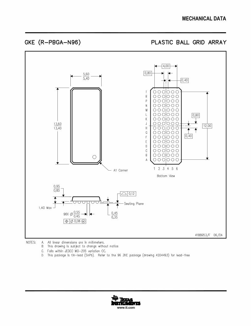
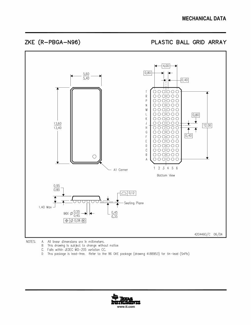
GKE PACKAGE(TOP VIEW)
1 2 3 4 5 6
A
B
C
D
E
F
G
H
J
K
L
M
N
P
R
T

SCES622 – JANUARY 2005
3POST OFFICE BOX 655303 • DALLAS, TEXAS 75265
logic diagram (positive logic)
1A1 SW 1B1
1A8
1OE
SW 1B8
3A1 SW 3B1
3A8
3OE
SW 3B8
A5
D6
A4
J5
M6
J4
A2
D1
J2
M1
2A1 SW 2B1
2A8
2OE
SW 2B8
4A1 SW 4B1
4A8
4OE
SW 4B8
E5
H5
H4
N5
T5
T4
E2
H2
N2
T2
simplified schematic, each FET switch (SW)
A
EN†
B
† EN is the internal enable signal applied to the switch.
ChargePump
VCC
SCES622 – JANUARY 2005
4 POST OFFICE BOX 655303 • DALLAS, TEXAS 75265
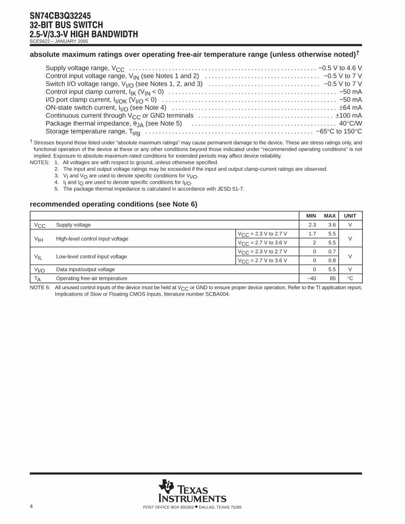
absolute maximum ratings over operating free-air temperature range (unless otherwise noted) †
Supply voltage range, VCC −0.5 V to 4.6 V. . . . . . . . . . . . . . . . . . . . . . . . . . . . . . . . . . . . . . . . . . . . . . . . . . . . . . . . . Control input voltage range, VIN (see Notes 1 and 2) −0.5 V to 7 V. . . . . . . . . . . . . . . . . . . . . . . . . . . . . . . . . . . Switch I/O voltage range, VI/O (see Notes 1, 2, and 3) −0.5 V to 7 V. . . . . . . . . . . . . . . . . . . . . . . . . . . . . . . . . . Control input clamp current, IIK (VIN < 0) −50 mA. . . . . . . . . . . . . . . . . . . . . . . . . . . . . . . . . . . . . . . . . . . . . . . . . . . I/O port clamp current, II/OK (VI/O < 0) −50 mA. . . . . . . . . . . . . . . . . . . . . . . . . . . . . . . . . . . . . . . . . . . . . . . . . . . . . ON-state switch current, II/O (see Note 4) ±64 mA. . . . . . . . . . . . . . . . . . . . . . . . . . . . . . . . . . . . . . . . . . . . . . . . . . Continuous current through VCC or GND terminals ±100 mA. . . . . . . . . . . . . . . . . . . . . . . . . . . . . . . . . . . . . . . . . Package thermal impedance, θJA (see Note 5) 40°C/W. . . . . . . . . . . . . . . . . . . . . . . . . . . . . . . . . . . . . . . . . . . . Storage temperature range, Tstg −65°C to 150°C. . . . . . . . . . . . . . . . . . . . . . . . . . . . . . . . . . . . . . . . . . . . . . . . . . .
† Stresses beyond those listed under “absolute maximum ratings” may cause permanent damage to the device. These are stress ratings only, andfunctional operation of the device at these or any other conditions beyond those indicated under “recommended operating conditions” is notimplied. Exposure to absolute-maximum-rated conditions for extended periods may affect device reliability.
NOTES: 1. All voltages are with respect to ground, unless otherwise specified.2. The input and output voltage ratings may be exceeded if the input and output clamp-current ratings are observed.3. VI and VO are used to denote specific conditions for VI/O.4. II and IO are used to denote specific conditions for II/O.5. The package thermal impedance is calculated in accordance with JESD 51-7.
recommended operating conditions (see Note 6)
MIN MAX UNIT
VCC Supply voltage 2.3 3.6 V
VIH High-level control input voltageVCC = 2.3 V to 2.7 V 1.7 5.5
VVIH High-level control input voltageVCC = 2.7 V to 3.6 V 2 5.5
V
VIL Low-level control input voltageVCC = 2.3 V to 2.7 V 0 0.7
VVIL Low-level control input voltageVCC = 2.7 V to 3.6 V 0 0.8
V
VI/O Data input/output voltage 0 5.5 V
TA Operating free-air temperature −40 85 °C
NOTE 6: All unused control inputs of the device must be held at VCC or GND to ensure proper device operation. Refer to the TI application report,Implications of Slow or Floating CMOS Inputs, literature number SCBA004.
SCES622 – JANUARY 2005
5POST OFFICE BOX 655303 • DALLAS, TEXAS 75265
electrical characteristics over recommended operating free-air temperature range (unlessotherwise noted)
PARAMETER TEST CONDITIONS MIN TYP† MAX UNIT
VIK VCC = 3.6 V, II = −18 mA −1.8 V
IIN Control inputs VCC = 3.6 V, VIN = 0 to 5.5 V ±1 µA
IOZ‡ VCC = 3.6 V,VO = 0 to 5.5 V,VI = 0,
Switch OFF,VIN = VCC or GND
±1 µA
Ioff VCC = 0, VO = 0 to 5.5 V, VI = 0 1 µA
ICC VCC = 3.6 V,II/O = 0,Switch ON or OFF,
VIN = VCC or GND 2 4 mA
∆ICC§ Control inputs VCC = 3.6 V, One input at 3 V, Other inputs at VCC or GND 30 µA
ICCD¶ Per controlinput
VCC = 3.6 V, A and B ports open,0.15 0.25
mA/MHz
ICCD¶ Per controlinput Control input switching at 50% duty cycle
0.15 0.25mA/MHz
Cin Control inputs VCC = 3.3 V, VIN = 5.5 V, 3.3 V, or 0 3.5 5 pF
Cio(OFF) VCC = 3.3 V,Switch OFF,VIN = VCC or GND,
VI/O = 5.5 V, 3.3 V, or 0 4 6 pF
Cio(ON) VCC = 3.3 V,Switch ON,VIN = VCC or GND,
VI/O = 5.5 V, 3.3 V, or 0 10 13 pF
VCC = 2.3 V, VI = 0, IO = 30 mA 6 8
ron#
VCC = 2.3 V,TYP at VCC = 2.5 V VI = 1.7 V, IO = −15 mA 5 10
Ωron#
VCC = 3 VVI = 0, IO = 30 mA 6 8
Ω
VCC = 3 VVI = 2.4 V, IO = −15 mA 5 9
VIN and IIN refer to control inputs. VI, VO, II, and IO refer to data pins.† All typical values are at VCC = 3.3 V (unless otherwise noted), TA = 25°C.‡ For I/O ports, the parameter IOZ includes the input leakage current.§ This is the increase in supply current for each input that is at the specified TTL voltage level, rather than VCC or GND.¶ This parameter specifies the dynamic power-supply current associated with the operating frequency of a single control input (see Figure 2).# Measured by the voltage drop between the A and B terminals at the indicated current through the switch. ON-state resistance is determined by
the lower of the voltages of the two (A or B) terminals.
switching characteristics over recommended operating free-air temperature range (unlessotherwise noted) (see Figure 3)
PARAMETERFROM
(INPUT)TO
(OUTPUT)
VCC = 2.5 V± 0.2 V
VCC = 3.3 V± 0.3 V UNITPARAMETER
(INPUT) (OUTPUT)MIN MAX MIN MAX
UNIT
fOE|| OE A or B 10 20 MHz
tpd A or B B or A 0.18 0.3 ns
ten OE A or B 1.5 8 1.5 7 ns
tdis OE A or B 1 8 1 7 ns
|| Maximum switching frequency for control input (VO > VCC, VI = 5 V, RL ≥ 1 MΩ, CL = 0)The propagation delay is the calculated RC time constant of the typical ON-state resistance of the switch and the specified load capacitance,
when driven by an ideal voltage source (zero output impedance).
SCES622 – JANUARY 2005
6 POST OFFICE BOX 655303 • DALLAS, TEXAS 75265
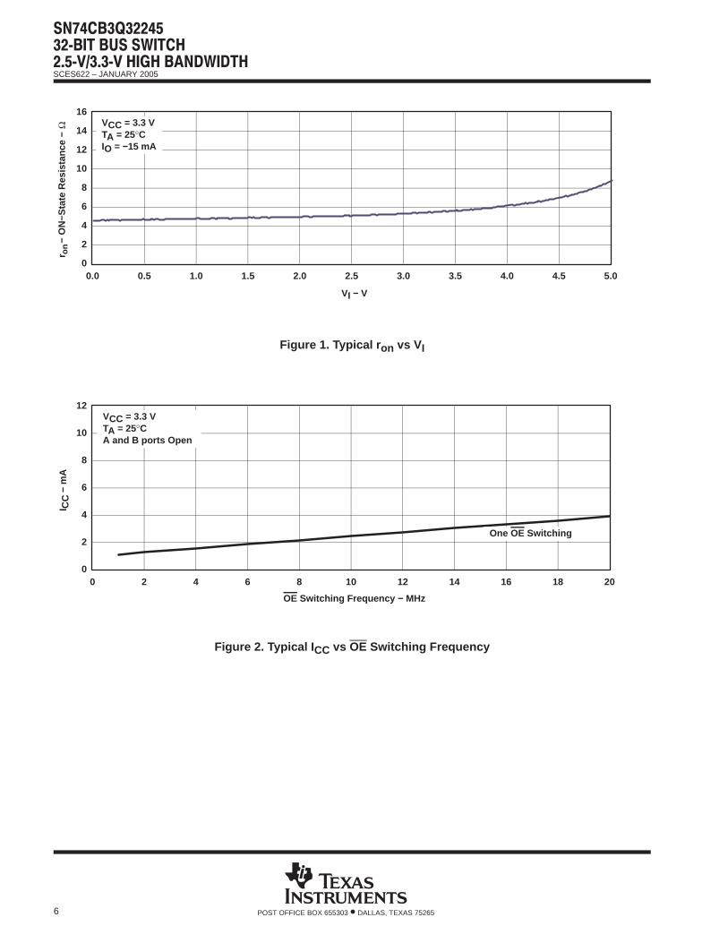
0
2
4
6
8
10
12
14
16
0.0 0.5 1.0 1.5 2.0 2.5 3.0 3.5 4.0 4.5 5.0
r on
− O
N−S
tate
Res
ista
nce
−
VI − V
Ω VCC = 3.3 VTA = 25°CIO = −15 mA
Figure 1. Typical r on vs VI
0
2
4
6
8
10
12
0 2 4 6 8 10 12 14 16 18 20
OE Switching Frequency − MHz
CC
I−
mA
VCC = 3.3 VTA = 25°CA and B ports Open
One OE Switching
Figure 2. Typical I CC vs OE Switching Frequency

SCES622 – JANUARY 2005
7POST OFFICE BOX 655303 • DALLAS, TEXAS 75265
PARAMETER MEASUREMENT INFORMATION
VOH
VOL
CL(see Note A)
TEST CIRCUIT
S12 × VCC
Open
GND
RL
RL
tPLH tPHL
OutputWaveform 1
S1 at 2 × VCC(see Note B)
OutputWaveform 2
S1 at GND(see Note B)
tPZL
tPZH
tPLZ
tPHZ
VCC
0 V
VOH
VOL
0 V
VOL + V∆
VOH − V∆
0 V
OutputControl
(VIN)
VCC
VCC
VOLTAGE WAVEFORMSPROPAGATION DELAY TIMES (t pd(s) )
VOLTAGE WAVEFORMSENABLE AND DISABLE TIMES
Output
NOTES: A. CL includes probe and jig capacitance.B. Waveform 1 is for an output with internal conditions such that the output is low, except when disabled by the output control.
Waveform 2 is for an output with internal conditions such that the output is high, except when disabled by the output control.C. All input pulses are supplied by generators having the following characteristics: PRR ≤ 10 MHz, ZO = 50 Ω, tr ≤ 2.5 ns, tf ≤ 2.5 ns.D. The outputs are measured one at a time, with one transition per measurement.E. tPLZ and tPHZ are the same as tdis.F. tPZL and tPZH are the same as ten.G. tPLH and tPHL are the same as tpd(s). The tpd propagation delay is the calculated RC time constant of the typical ON-state
resistance of the switch and the specified load capacitance, when driven by an ideal voltage source (zero output impedance).H. All parameters and waveforms are not applicable to all devices.
50 ΩVG1
VCC
DUT
50 Ω
VIN
50 ΩVG2 50 Ω
VI
TEST RLS1 V∆CL
2.5 V ± 0.2 V3.3 V ± 0.3 V
VCC VI
tPHZ/tPZH
tPLZ/tPZL
tpd(s)
2.5 V ± 0.2 V3.3 V ± 0.3 V
2.5 V ± 0.2 V3.3 V ± 0.3 V
OpenOpen
2 × VCC2 × VCC
GNDGND
500 Ω500 Ω
500 Ω500 Ω
500 Ω500 Ω
VCC or GNDVCC or GND
GNDGND
VCCVCC
30 pF50 pF
30 pF50 pF
30 pF50 pF
0.15 V0.3 V
0.15 V0.3 V
OutputControl
(VIN)
Input Generator
Input Generator
VCC/2 VCC/2
VCC/2 VCC/2
VCC/2 VCC/2 VCC/2
VCC/2
VO
Figure 3. Test Circuit and Voltage Waveforms

PACKAGE OPTION ADDENDUM
www.ti.com 11-Apr-2013
Addendum-Page 1
PACKAGING INFORMATION
Orderable Device Status(1)
Package Type PackageDrawing
Pins PackageQty
Eco Plan(2)
Lead/Ball Finish MSL Peak Temp(3)
Op Temp (°C) Top-Side Markings(4)
Samples
SN74CB3Q32245GKER NRND LFBGA GKE 96 1000 TBD SNPB Level-2-235C-1 YEAR -40 to 85 BZ245
SN74CB3Q32245ZKER ACTIVE LFBGA ZKE 96 1000 Green (RoHS& no Sb/Br)
SNAGCU Level-3-260C-168 HR -40 to 85 BZ245
(1) The marketing status values are defined as follows:ACTIVE: Product device recommended for new designs.LIFEBUY: TI has announced that the device will be discontinued, and a lifetime-buy period is in effect.NRND: Not recommended for new designs. Device is in production to support existing customers, but TI does not recommend using this part in a new design.PREVIEW: Device has been announced but is not in production. Samples may or may not be available.OBSOLETE: TI has discontinued the production of the device.
(2) Eco Plan - The planned eco-friendly classification: Pb-Free (RoHS), Pb-Free (RoHS Exempt), or Green (RoHS & no Sb/Br) - please check http://www.ti.com/productcontent for the latest availabilityinformation and additional product content details.TBD: The Pb-Free/Green conversion plan has not been defined.Pb-Free (RoHS): TI's terms "Lead-Free" or "Pb-Free" mean semiconductor products that are compatible with the current RoHS requirements for all 6 substances, including the requirement thatlead not exceed 0.1% by weight in homogeneous materials. Where designed to be soldered at high temperatures, TI Pb-Free products are suitable for use in specified lead-free processes.Pb-Free (RoHS Exempt): This component has a RoHS exemption for either 1) lead-based flip-chip solder bumps used between the die and package, or 2) lead-based die adhesive used betweenthe die and leadframe. The component is otherwise considered Pb-Free (RoHS compatible) as defined above.Green (RoHS & no Sb/Br): TI defines "Green" to mean Pb-Free (RoHS compatible), and free of Bromine (Br) and Antimony (Sb) based flame retardants (Br or Sb do not exceed 0.1% by weightin homogeneous material)
(3) MSL, Peak Temp. -- The Moisture Sensitivity Level rating according to the JEDEC industry standard classifications, and peak solder temperature.
(4) Multiple Top-Side Markings will be inside parentheses. Only one Top-Side Marking contained in parentheses and separated by a "~" will appear on a device. If a line is indented then it is acontinuation of the previous line and the two combined represent the entire Top-Side Marking for that device.
Important Information and Disclaimer:The information provided on this page represents TI's knowledge and belief as of the date that it is provided. TI bases its knowledge and belief on informationprovided by third parties, and makes no representation or warranty as to the accuracy of such information. Efforts are underway to better integrate information from third parties. TI has taken andcontinues to take reasonable steps to provide representative and accurate information but may not have conducted destructive testing or chemical analysis on incoming materials and chemicals.TI and TI suppliers consider certain information to be proprietary, and thus CAS numbers and other limited information may not be available for release.
In no event shall TI's liability arising out of such information exceed the total purchase price of the TI part(s) at issue in this document sold by TI to Customer on an annual basis.

TAPE AND REEL INFORMATION
*All dimensions are nominal
Device PackageType
PackageDrawing
Pins SPQ ReelDiameter
(mm)
ReelWidth
W1 (mm)
A0(mm)
B0(mm)
K0(mm)
P1(mm)
W(mm)
Pin1Quadrant
SN74CB3Q32245GKER LFBGA GKE 96 1000 330.0 24.4 5.7 13.7 2.0 8.0 24.0 Q1
SN74CB3Q32245ZKER LFBGA ZKE 96 1000 330.0 24.4 5.7 13.7 2.0 8.0 24.0 Q1
PACKAGE MATERIALS INFORMATION
www.ti.com 22-Jan-2015
Pack Materials-Page 1
*All dimensions are nominal
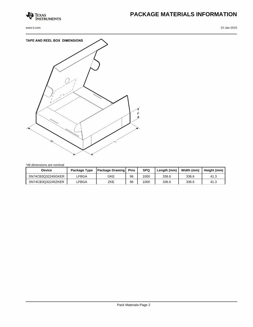
Device Package Type Package Drawing Pins SPQ Length (mm) Width (mm) Height (mm)
SN74CB3Q32245GKER LFBGA GKE 96 1000 336.6 336.6 41.3
SN74CB3Q32245ZKER LFBGA ZKE 96 1000 336.6 336.6 41.3
PACKAGE MATERIALS INFORMATION
www.ti.com 22-Jan-2015
Pack Materials-Page 2

IMPORTANT NOTICE
Texas Instruments Incorporated and its subsidiaries (TI) reserve the right to make corrections, enhancements, improvements and otherchanges to its semiconductor products and services per JESD46, latest issue, and to discontinue any product or service per JESD48, latestissue. Buyers should obtain the latest relevant information before placing orders and should verify that such information is current andcomplete. All semiconductor products (also referred to herein as “components”) are sold subject to TI’s terms and conditions of salesupplied at the time of order acknowledgment.TI warrants performance of its components to the specifications applicable at the time of sale, in accordance with the warranty in TI’s termsand conditions of sale of semiconductor products. Testing and other quality control techniques are used to the extent TI deems necessaryto support this warranty. Except where mandated by applicable law, testing of all parameters of each component is not necessarilyperformed.TI assumes no liability for applications assistance or the design of Buyers’ products. Buyers are responsible for their products andapplications using TI components. To minimize the risks associated with Buyers’ products and applications, Buyers should provideadequate design and operating safeguards.TI does not warrant or represent that any license, either express or implied, is granted under any patent right, copyright, mask work right, orother intellectual property right relating to any combination, machine, or process in which TI components or services are used. Informationpublished by TI regarding third-party products or services does not constitute a license to use such products or services or a warranty orendorsement thereof. Use of such information may require a license from a third party under the patents or other intellectual property of thethird party, or a license from TI under the patents or other intellectual property of TI.Reproduction of significant portions of TI information in TI data books or data sheets is permissible only if reproduction is without alterationand is accompanied by all associated warranties, conditions, limitations, and notices. TI is not responsible or liable for such altereddocumentation. Information of third parties may be subject to additional restrictions.Resale of TI components or services with statements different from or beyond the parameters stated by TI for that component or servicevoids all express and any implied warranties for the associated TI component or service and is an unfair and deceptive business practice.TI is not responsible or liable for any such statements.Buyer acknowledges and agrees that it is solely responsible for compliance with all legal, regulatory and safety-related requirementsconcerning its products, and any use of TI components in its applications, notwithstanding any applications-related information or supportthat may be provided by TI. Buyer represents and agrees that it has all the necessary expertise to create and implement safeguards whichanticipate dangerous consequences of failures, monitor failures and their consequences, lessen the likelihood of failures that might causeharm and take appropriate remedial actions. Buyer will fully indemnify TI and its representatives against any damages arising out of the useof any TI components in safety-critical applications.In some cases, TI components may be promoted specifically to facilitate safety-related applications. With such components, TI’s goal is tohelp enable customers to design and create their own end-product solutions that meet applicable functional safety standards andrequirements. Nonetheless, such components are subject to these terms.No TI components are authorized for use in FDA Class III (or similar life-critical medical equipment) unless authorized officers of the partieshave executed a special agreement specifically governing such use.Only those TI components which TI has specifically designated as military grade or “enhanced plastic” are designed and intended for use inmilitary/aerospace applications or environments. Buyer acknowledges and agrees that any military or aerospace use of TI componentswhich have not been so designated is solely at the Buyer's risk, and that Buyer is solely responsible for compliance with all legal andregulatory requirements in connection with such use.TI has specifically designated certain components as meeting ISO/TS16949 requirements, mainly for automotive use. In any case of use ofnon-designated products, TI will not be responsible for any failure to meet ISO/TS16949.
Products ApplicationsAudio www.ti.com/audio Automotive and Transportation www.ti.com/automotiveAmplifiers amplifier.ti.com Communications and Telecom www.ti.com/communicationsData Converters dataconverter.ti.com Computers and Peripherals www.ti.com/computersDLP® Products www.dlp.com Consumer Electronics www.ti.com/consumer-appsDSP dsp.ti.com Energy and Lighting www.ti.com/energyClocks and Timers www.ti.com/clocks Industrial www.ti.com/industrialInterface interface.ti.com Medical www.ti.com/medicalLogic logic.ti.com Security www.ti.com/securityPower Mgmt power.ti.com Space, Avionics and Defense www.ti.com/space-avionics-defenseMicrocontrollers microcontroller.ti.com Video and Imaging www.ti.com/videoRFID www.ti-rfid.comOMAP Applications Processors www.ti.com/omap TI E2E Community e2e.ti.comWireless Connectivity www.ti.com/wirelessconnectivity
Mailing Address: Texas Instruments, Post Office Box 655303, Dallas, Texas 75265Copyright © 2015, Texas Instruments Incorporated