Embed Size (px)
Citation preview
© Copyright Lime Microsystems Proprietary and Confidential
Lime Microsystems Limited Longdene House Hedgehog Lane Haslemere Surrey GU27 2PH United Kingdom Tel: +44 (0) 1428-653-335 Fax: +44 (0) 1483-683-481 e-mail: [email protected]
LMS6002 – Wide Band Multi Standard Radio Chip in 0.18um BiCMOS
- Programming and Calibration Guide -
Chip version: LMS6002D Chip revision: r2 Document version: 1.1 Document revision: 1 Last modified: 28/10/2010 10:07:00

i
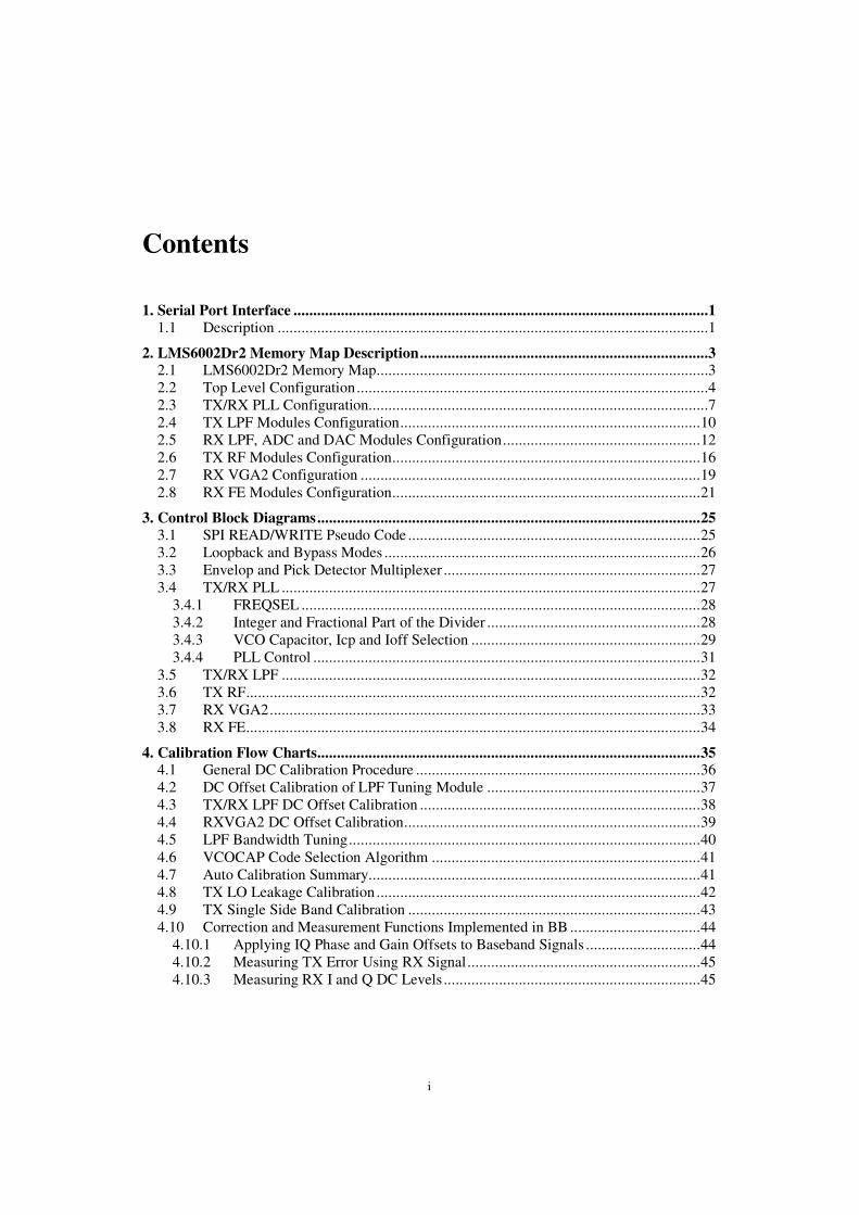
Contents
1. Serial Port Interface .........................................................................................................1 1.1 Description .............................................................................................................1
2. LMS6002Dr2 Memory Map Description.........................................................................3 2.1 LMS6002Dr2 Memory Map....................................................................................3 2.2 Top Level Configuration.........................................................................................4 2.3 TX/RX PLL Configuration......................................................................................7 2.4 TX LPF Modules Configuration............................................................................10 2.5 RX LPF, ADC and DAC Modules Configuration..................................................12 2.6 TX RF Modules Configuration..............................................................................16 2.7 RX VGA2 Configuration ......................................................................................19 2.8 RX FE Modules Configuration..............................................................................21
3. Control Block Diagrams.................................................................................................25 3.1 SPI READ/WRITE Pseudo Code ..........................................................................25 3.2 Loopback and Bypass Modes ................................................................................26 3.3 Envelop and Pick Detector Multiplexer .................................................................27 3.4 TX/RX PLL ..........................................................................................................27
3.4.1 FREQSEL .....................................................................................................28 3.4.2 Integer and Fractional Part of the Divider ......................................................28 3.4.3 VCO Capacitor, Icp and Ioff Selection ..........................................................29 3.4.4 PLL Control ..................................................................................................31
3.5 TX/RX LPF ..........................................................................................................32 3.6 TX RF...................................................................................................................32 3.7 RX VGA2.............................................................................................................33 3.8 RX FE...................................................................................................................34
4. Calibration Flow Charts.................................................................................................35 4.1 General DC Calibration Procedure ........................................................................36 4.2 DC Offset Calibration of LPF Tuning Module ......................................................37 4.3 TX/RX LPF DC Offset Calibration .......................................................................38 4.4 RXVGA2 DC Offset Calibration...........................................................................39 4.5 LPF Bandwidth Tuning.........................................................................................40 4.6 VCOCAP Code Selection Algorithm ....................................................................41 4.7 Auto Calibration Summary....................................................................................41 4.8 TX LO Leakage Calibration ..................................................................................42 4.9 TX Single Side Band Calibration ..........................................................................43 4.10 Correction and Measurement Functions Implemented in BB .................................44
4.10.1 Applying IQ Phase and Gain Offsets to Baseband Signals .............................44 4.10.2 Measuring TX Error Using RX Signal...........................................................45 4.10.3 Measuring RX I and Q DC Levels .................................................................45

LMS6002 – Wide Band Multi Standard Radio Chip in 0.18um BiCMOS Programming and Calibration Guide
ii
Revision History Version 1.0r0 Released: Mar 16, 2010 Initial version constructed from new SPI and old 6002D programming guide documents.
Version 1.0r1 Released: Apr 15, 2010 Unnoticed change in 0x5F register documented
Version 1.1r0 Released: Oct 27, 2010 FREQSEL table updated. Calibration diagrams updated. VCOCAP selection algorithm added. Version 1.1r1 Released: Oct 28, 2010 Diagram 4.3 corrected.
1
11 Serial Port Interface
1.1 Description
The functionality of LMS6002 transceiver is fully controlled by a set of internal registers which can be accessed through a serial port interface. Both write and read operations are supported. The serial port can be configured to run in 3 or 4 wire mode with the following pins used:
• SEN serial port enable, active low;
• SCLK serial clock;
• SDIO serial data in/out in 3 wire mode, serial data input in 4 wire mode;
• SDO serial data out in 4 wire mode, don’t care in 3 wire mode. Serial port key features:
• 16 serial clock cycles are required to complete write operation;
• 16 serial clock cycles are required to complete read operation;
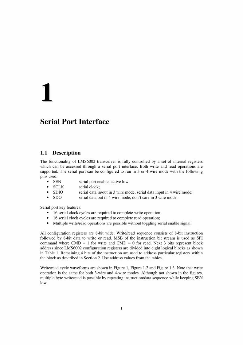
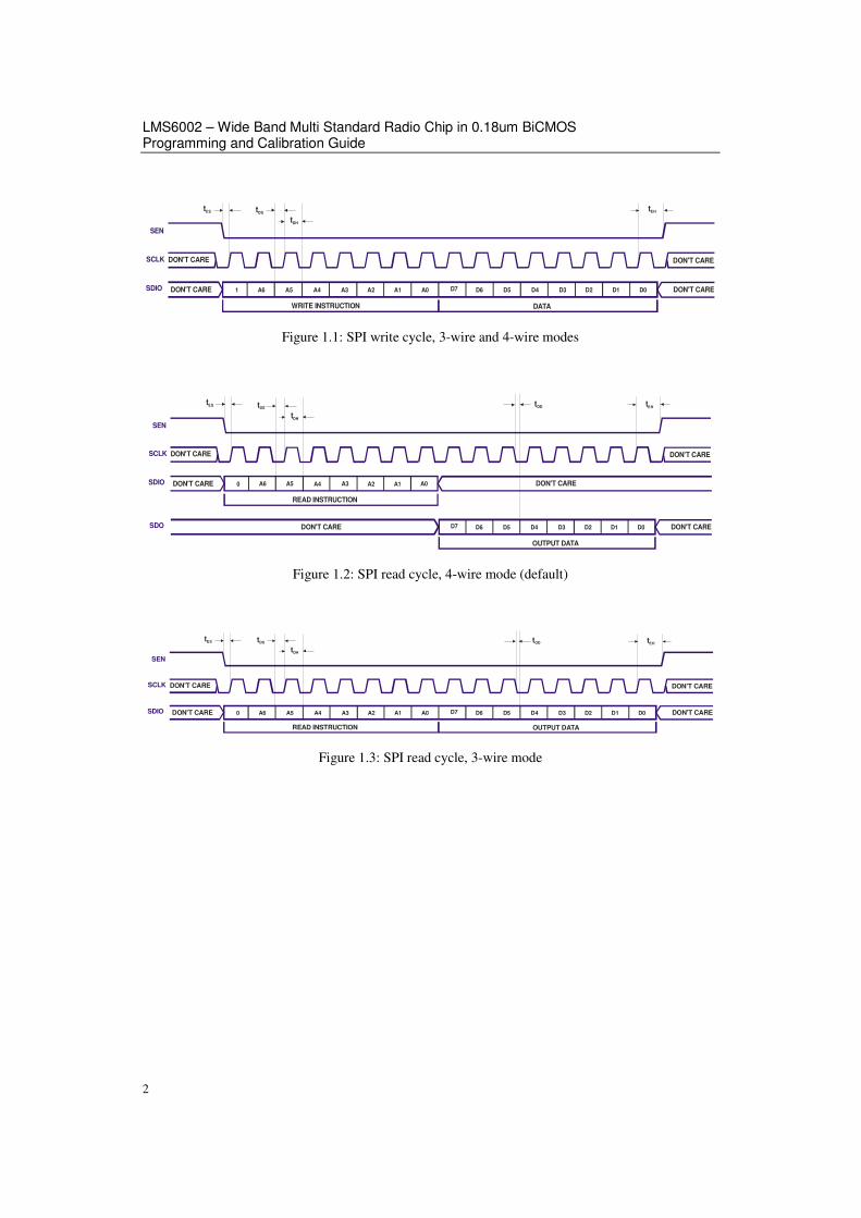
• Multiple write/read operations are possible without toggling serial enable signal. All configuration registers are 8-bit wide. Write/read sequence consists of 8-bit instruction followed by 8-bit data to write or read. MSB of the instruction bit stream is used as SPI command where CMD = 1 for write and CMD = 0 for read. Next 3 bits represent block address since LMS6002 configuration registers are divided into eight logical blocks as shown in Table 1. Remaining 4 bits of the instruction are used to address particular registers within the block as described in Section 2. Use address values from the tables. Write/read cycle waveforms are shown in Figure 1, Figure 1.2 and Figure 1.3. Note that write operation is the same for both 3-wire and 4-wire modes. Although not shown in the figures, multiple byte write/read is possible by repeating instruction/data sequence while keeping SEN low.
LMS6002 – Wide Band Multi Standard Radio Chip in 0.18um BiCMOS Programming and Calibration Guide
2
DON'T CARE DON'T CARESCLK
SEN
SDIO DON'T CARE DON'T CARE
WRITE INSTRUCTION DATA
1 A6 A5 A4 A3 A2 A1 A0 D7 D6 D5 D4 D3 D2 D1 D0
tES tDS
tDH
tEH
Figure 1.1: SPI write cycle, 3-wire and 4-wire modes
DON'T CARE DON'T CARESCLK
SEN
SDIO DON'T CARE DON'T CARE
READ INSTRUCTION
0 A6 A5 A4 A3 A2 A1 A0
SDO DON'T CARE DON'T CARE
OUTPUT DATA
D7 D6 D5 D4 D3 D2 D1 D0
tES tDS
tDH
tEHtOD
Figure 1.2: SPI read cycle, 4-wire mode (default)
DON'T CARE DON'T CARESCLK
SEN
SDIO DON'T CARE DON'T CARE
READ INSTRUCTION OUTPUT DATA
0 A6 A5 A4 A3 A2 A1 A0 D7 D6 D5 D4 D3 D2 D1 D0
tES tDS
tDH
tOD tEH
Figure 1.3: SPI read cycle, 3-wire mode
3
22 LMS6002Dr2 Memory Map Description
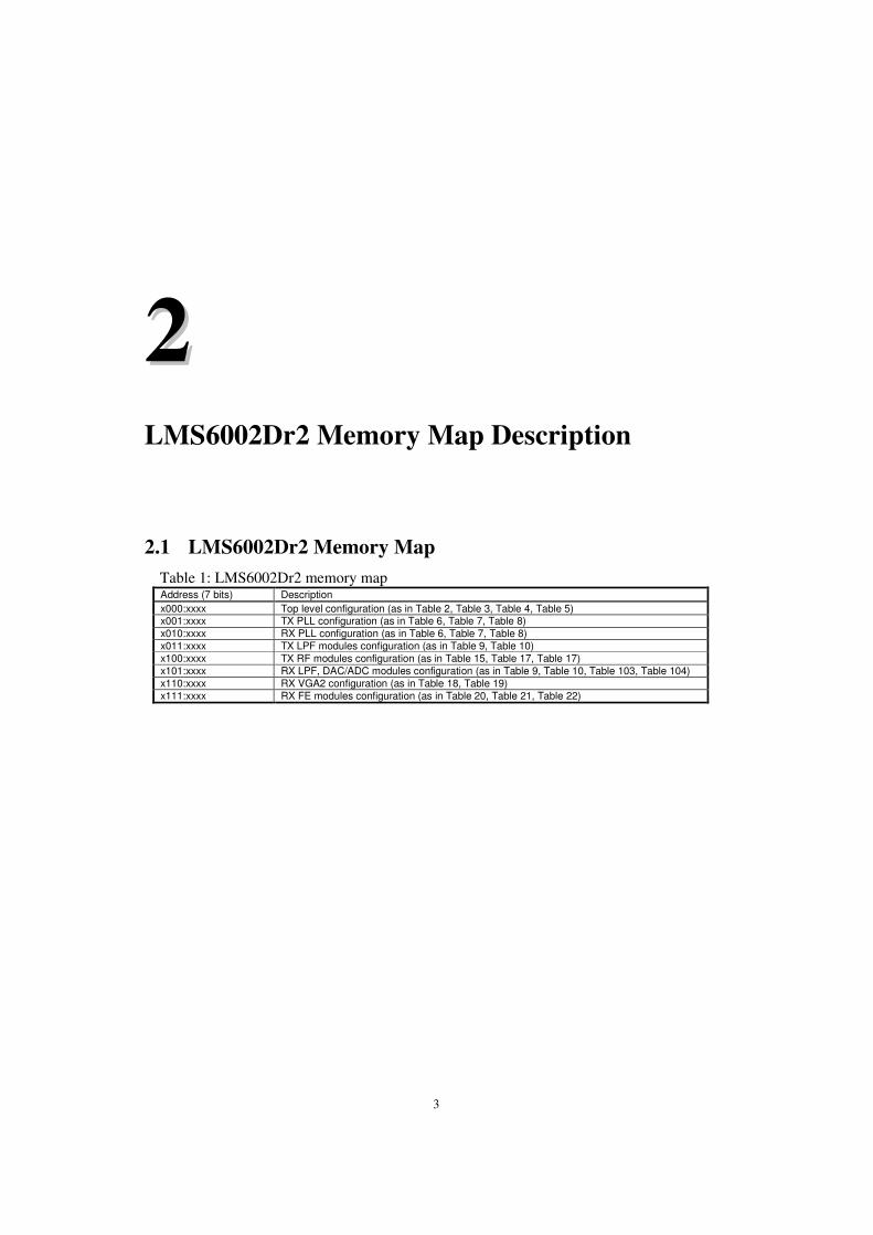
2.1 LMS6002Dr2 Memory Map
Table 1: LMS6002Dr2 memory map Address (7 bits) Description
x000:xxxx Top level configuration (as in Table 2, Table 3, Table 4, Table 5) x001:xxxx TX PLL configuration (as in Table 6, Table 7, Table 8) x010:xxxx RX PLL configuration (as in Table 6, Table 7, Table 8) x011:xxxx TX LPF modules configuration (as in Table 9, Table 10) x100:xxxx TX RF modules configuration (as in Table 15, Table 17, Table 17) x101:xxxx RX LPF, DAC/ADC modules configuration (as in Table 9, Table 10, Table 103, Table 104) x110:xxxx RX VGA2 configuration (as in Table 18, Table 19) x111:xxxx RX FE modules configuration (as in Table 20, Table 21, Table 22)
LMS6002 – Wide Band Multi Standard Radio Chip in 0.18um BiCMOS Programming and Calibration Guide
4
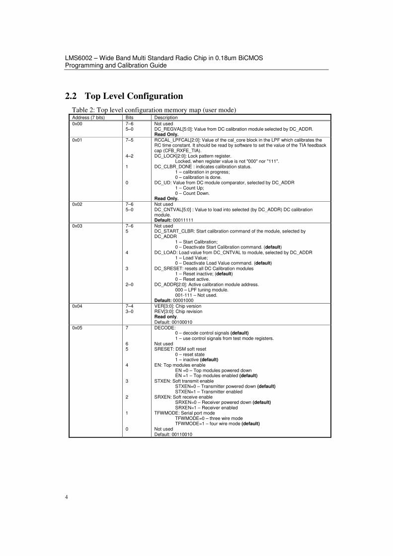
2.2 Top Level Configuration
Table 2: Top level configuration memory map (user mode) Address (7 bits) Bits Description
0x00 7–6 5–0
Not used DC_REGVAL[5:0]: Value from DC calibration module selected by DC_ADDR. Read Only.
0x01 7–5 4–2 1 0
RCCAL_LPFCAL[2:0]: Value of the cal_core block in the LPF which calibrates the RC time constant. It should be read by software to set the value of the TIA feedback cap (CFB_RXFE_TIA). DC_LOCK[2:0]: Lock pattern register. Locked, when register value is not "000" nor "111". DC_CLBR_DONE : indicates calibration status. 1 – calibration in progress; 0 – calibration is done. DC_UD: Value from DC module comparator, selected by DC_ADDR 1 – Count Up; 0 – Count Down. Read Only.
0x02 7–6 5–0
Not used DC_CNTVAL[5:0] : Value to load into selected (by DC_ADDR) DC calibration module. Default: 00011111
0x03 7–6 5 4 3 2–0
Not used DC_START_CLBR: Start calibration command of the module, selected by DC_ADDR 1 – Start Calibration; 0 – Deactivate Start Calibration command. (default) DC_LOAD: Load value from DC_CNTVAL to module, selected by DC_ADDR 1 – Load Value; 0 – Deactivate Load Value command. (default) DC_SRESET: resets all DC Calibration modules 1 – Reset inactive; (default) 0 – Reset active. DC_ADDR[2:0]: Active calibration module address. 000 – LPF tuning module. 001-111 – Not used. Default: 00001000
0x04 7–4 3–0
VER[3:0]: Chip version REV[3:0]: Chip revision Read only. Default: 00100010
0x05 7 6 5 4 3 2 1 0
DECODE: 0 – decode control signals (default) 1 – use control signals from test mode registers. Not used SRESET: DSM soft reset 0 – reset state 1 – inactive (default) EN: Top modules enable EN =0 – Top modules powered down EN =1 – Top modules enabled (default) STXEN: Soft transmit enable STXEN=0 – Transmitter powered down (default) STXEN=1 – Transmitter enabled SRXEN: Soft receive enable SRXEN=0 – Receiver powered down (default) SRXEN=1 – Receiver enabled TFWMODE: Serial port mode TFWMODE=0 – three wire mode TFWMODE=1 – four wire mode (default) Not used Default: 00110010
LMS6002Dr2 Memory Map Description
5
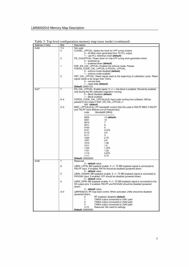
Table 3: Top level configuration memory map (user mode) (continued) Address (7 bits) Bits Description
0x06 7-4 3 2 1 0
Not used CLKSEL_LPFCAL: Select the clock for LPF tuning module 0 – 40 MHz clock generated from TX PLL output 1 – use PLL reference clock (default) PD_CLKLPFCAL: Power down on chip LPF tuning clock generation block 0 – powered up 1 – powered down (default) ENF_EN_CAL_LPFCAL: Enables the enforce mode. Passes FORCE_CODE_CAL_LPFCAL to RCCAL_LPFCAL. 0 – enforce mode disabled (default) 1 – enforce mode enabled RST_CAL_LPFCAL: Reset signal used at the beginning of calibration cycle. Reset signal needs to be longer than 100ns. 0 – normal state 1 – reset state (default) Default: 00001101
0x07 7 6–4 3–0
EN_CAL_LPFCAL: Enable signal. If =1--> the block is enabled. Should be enabled only during the RC calibration algorithm running. 0 – Block disabled (default) 1 – Block enabled FORCE_CODE_CAL_LPFCAL[2:0]: Input code coming from software. Will be passed to the output if ENF_EN_CAL_LPFCAL=1. 000 (default) BWC_LPFCAL[3:0]: LPF bandwidth control (Set this code to RXLPF BWC if RXLPF and TXLPF have different cut-off frequencies). code Bandwidth [MHz] ======================= 0000 14 (default) 0001 10 0010 7 0011 6 0100 5 0101 4.375 0110 3.5 0111 3 1000 2.75 1001 2.5 1010 1.92 1011 1.5 1100 1.375 1101 1.25 1110 0.875 1111 0.75 Default: 00000000
0x08 7 6 5 4 3–0
Reserved 0 – default value. LBEN_LPFIN: BB loopback enable. If =1, TX BB loopback signal is connected to RXLPF input. If enabled, RXTIA should be disabled (powered down) 0 – default value. LBEN_VGA2IN: BB loopback enable. If =1, TX BB loopback signal is connected to RXVGA2 input. If enabled, LPF should be disabled (powered down). 0 – default value. LBEN_OPIN: BB loopback enable. If =1, TX BB loopback signal is connected to the RX output pins. If enabled, RXLPF and RXVGA2 should be disabled (powered down) 0 – default value. LBRFEN[3:0]: RF loop back control. When activated, LNAs should be disabled (powered down). 0 RF loopback disabled (default) 1 TXMIX output connected to LNA1 path 2 TXMIX output connected to LNA2 path 3 TXMIX output connected to LNA3 path 4-15 Reserved. Not valid for settings. Default: 00000000
LMS6002 – Wide Band Multi Standard Radio Chip in 0.18um BiCMOS Programming and Calibration Guide
6
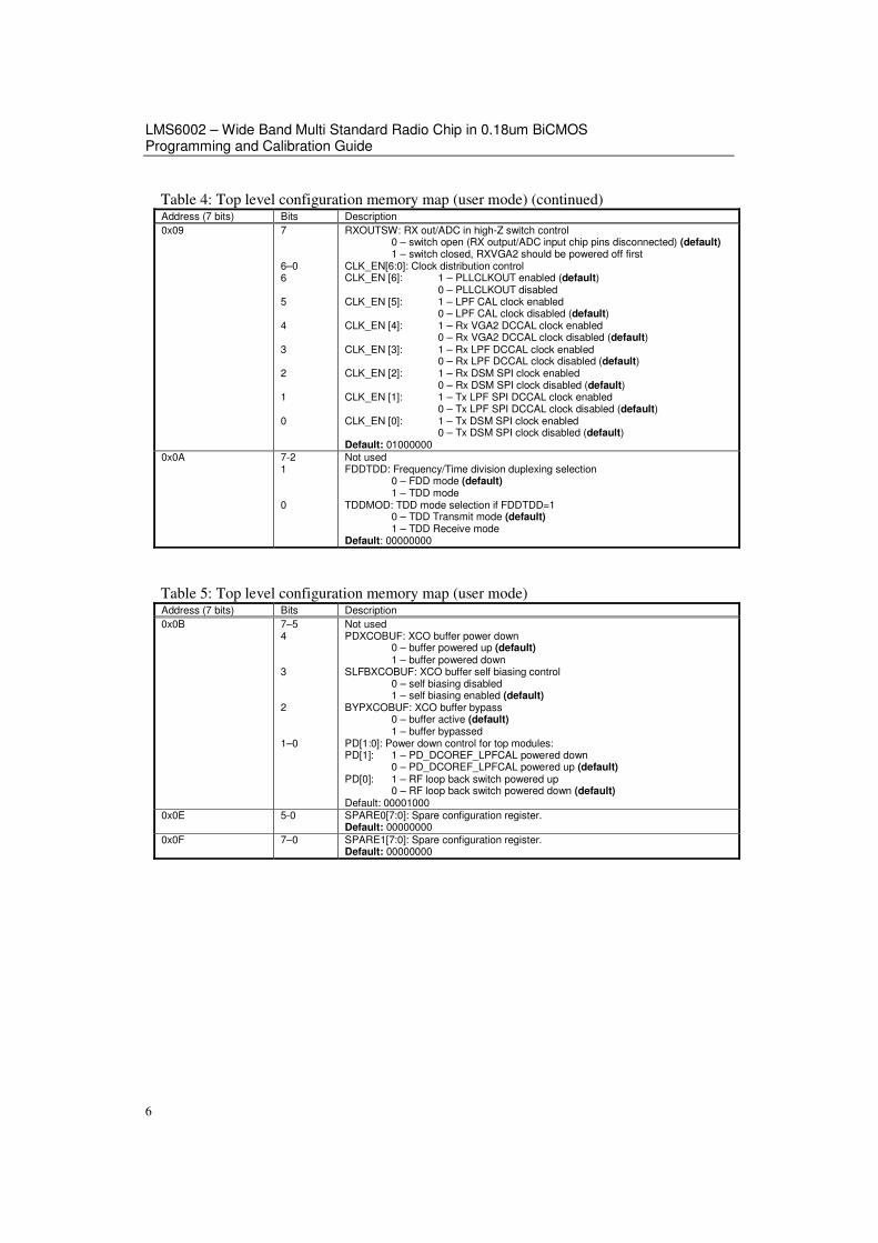
Table 4: Top level configuration memory map (user mode) (continued) Address (7 bits) Bits Description
0x09 7 6–0 6 5 4 3 2 1 0
RXOUTSW: RX out/ADC in high-Z switch control 0 – switch open (RX output/ADC input chip pins disconnected) (default) 1 – switch closed, RXVGA2 should be powered off first CLK_EN[6:0]: Clock distribution control CLK_EN [6]: 1 – PLLCLKOUT enabled (default) 0 – PLLCLKOUT disabled CLK_EN [5]: 1 – LPF CAL clock enabled 0 – LPF CAL clock disabled (default) CLK_EN [4]: 1 – Rx VGA2 DCCAL clock enabled 0 – Rx VGA2 DCCAL clock disabled (default) CLK_EN [3]: 1 – Rx LPF DCCAL clock enabled 0 – Rx LPF DCCAL clock disabled (default) CLK_EN [2]: 1 – Rx DSM SPI clock enabled 0 – Rx DSM SPI clock disabled (default) CLK_EN [1]: 1 – Tx LPF SPI DCCAL clock enabled 0 – Tx LPF SPI DCCAL clock disabled (default) CLK_EN [0]: 1 – Tx DSM SPI clock enabled 0 – Tx DSM SPI clock disabled (default) Default: 01000000
0x0A 7-2 1 0
Not used FDDTDD: Frequency/Time division duplexing selection 0 – FDD mode (default) 1 – TDD mode TDDMOD: TDD mode selection if FDDTDD=1 0 – TDD Transmit mode (default) 1 – TDD Receive mode Default: 00000000
Table 5: Top level configuration memory map (user mode) Address (7 bits) Bits Description
0x0B 7–5 4 3 2 1–0
Not used PDXCOBUF: XCO buffer power down 0 – buffer powered up (default) 1 – buffer powered down SLFBXCOBUF: XCO buffer self biasing control 0 – self biasing disabled 1 – self biasing enabled (default) BYPXCOBUF: XCO buffer bypass 0 – buffer active (default) 1 – buffer bypassed PD[1:0]: Power down control for top modules: PD[1]: 1 – PD_DCOREF_LPFCAL powered down 0 – PD_DCOREF_LPFCAL powered up (default) PD[0]: 1 – RF loop back switch powered up 0 – RF loop back switch powered down (default) Default: 00001000
0x0E 5-0 SPARE0[7:0]: Spare configuration register. Default: 00000000
0x0F
7–0 SPARE1[7:0]: Spare configuration register. Default: 00000000
LMS6002Dr2 Memory Map Description
7
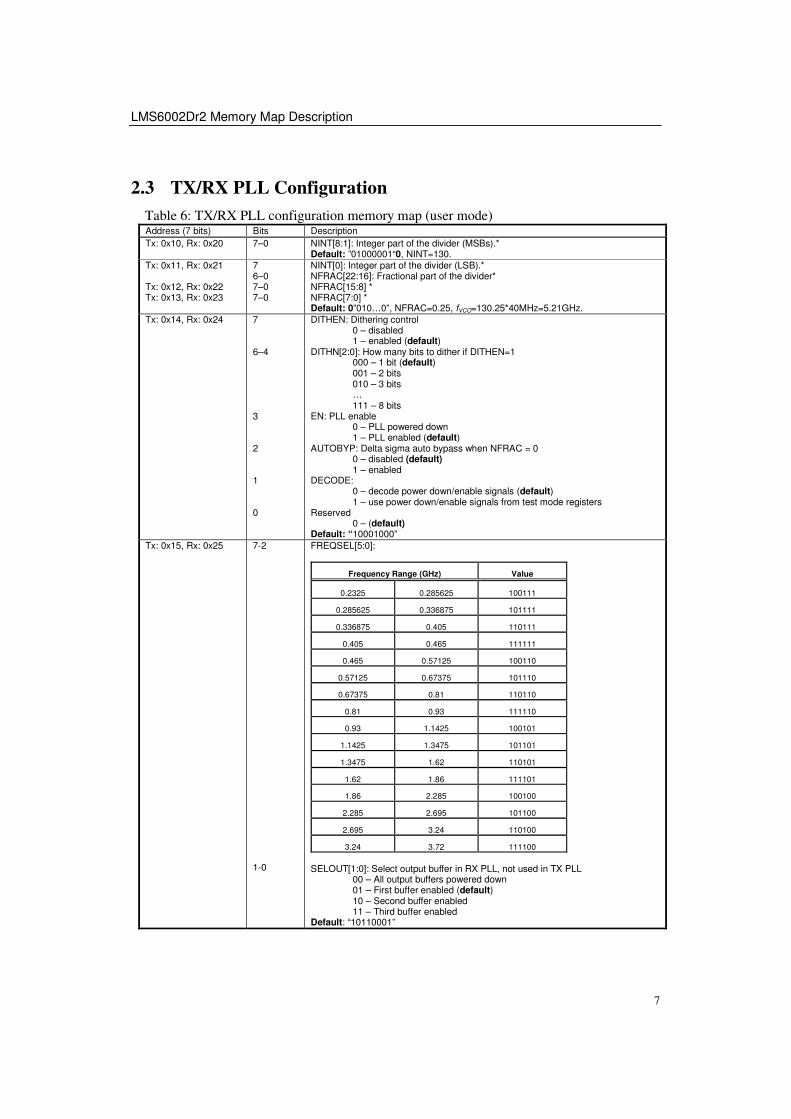
2.3 TX/RX PLL Configuration
Table 6: TX/RX PLL configuration memory map (user mode) Address (7 bits) Bits Description
Tx: 0x10, Rx: 0x20 7–0
NINT[8:1]: Integer part of the divider (MSBs).* Default: ”01000001“0, NINT=130.
Tx: 0x11, Rx: 0x21 Tx: 0x12, Rx: 0x22 Tx: 0x13, Rx: 0x23
7 6–0 7–0 7–0
NINT[0]: Integer part of the divider (LSB).* NFRAC[22:16]: Fractional part of the divider* NFRAC[15:8] * NFRAC[7:0] * Default: 0”010…0”, NFRAC=0.25, fVCO=130.25*40MHz=5.21GHz.
Tx: 0x14, Rx: 0x24 7 6–4 3 2 1 0
DITHEN: Dithering control 0 – disabled 1 – enabled (default) DITHN[2:0]: How many bits to dither if DITHEN=1 000 – 1 bit (default) 001 – 2 bits 010 – 3 bits … 111 – 8 bits EN: PLL enable 0 – PLL powered down 1 – PLL enabled (default) AUTOBYP: Delta sigma auto bypass when NFRAC = 0 0 – disabled (default) 1 – enabled DECODE: 0 – decode power down/enable signals (default) 1 – use power down/enable signals from test mode registers Reserved 0 – (default) Default: “10001000”
Tx: 0x15, Rx: 0x25
7-2 1-0
FREQSEL[5:0]:
Frequency Range (GHz) Value
0.2325 0.285625 100111
0.285625 0.336875 101111
0.336875 0.405 110111
0.405 0.465 111111
0.465 0.57125 100110
0.57125 0.67375 101110
0.67375 0.81 110110
0.81 0.93 111110
0.93 1.1425 100101
1.1425 1.3475 101101
1.3475 1.62 110101
1.62 1.86 111101
1.86 2.285 100100
2.285 2.695 101100
2.695 3.24 110100
3.24 3.72 111100
SELOUT[1:0]: Select output buffer in RX PLL, not used in TX PLL 00 – All output buffers powered down 01 – First buffer enabled (default) 10 – Second buffer enabled 11 – Third buffer enabled Default: “10110001”
LMS6002 – Wide Band Multi Standard Radio Chip in 0.18um BiCMOS Programming and Calibration Guide
8
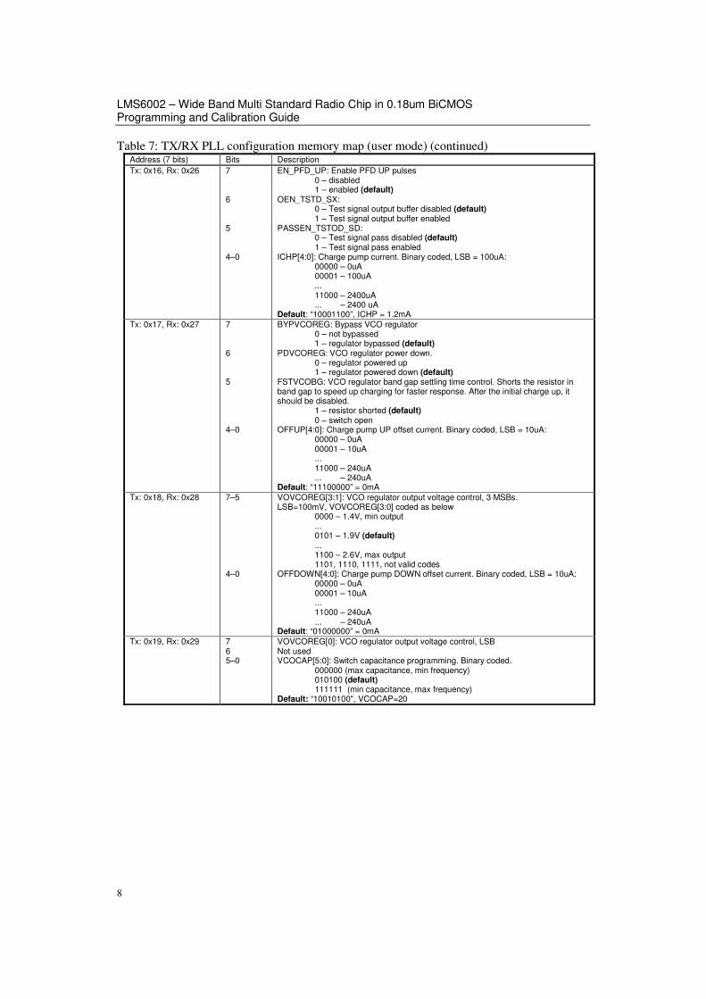
Table 7: TX/RX PLL configuration memory map (user mode) (continued) Address (7 bits) Bits Description
Tx: 0x16, Rx: 0x26 7 6 5 4–0
EN_PFD_UP: Enable PFD UP pulses 0 – disabled 1 – enabled (default) OEN_TSTD_SX: 0 – Test signal output buffer disabled (default) 1 – Test signal output buffer enabled PASSEN_TSTOD_SD: 0 – Test signal pass disabled (default) 1 – Test signal pass enabled ICHP[4:0]: Charge pump current. Binary coded, LSB = 100uA: 00000 – 0uA 00001 – 100uA ... 11000 – 2400uA ... – 2400 uA Default: “10001100”, ICHP = 1.2mA
Tx: 0x17, Rx: 0x27 7 6 5 4–0
BYPVCOREG: Bypass VCO regulator 0 – not bypassed 1 – regulator bypassed (default) PDVCOREG: VCO regulator power down. 0 – regulator powered up 1 – regulator powered down (default) FSTVCOBG: VCO regulator band gap settling time control. Shorts the resistor in band gap to speed up charging for faster response. After the initial charge up, it should be disabled. 1 – resistor shorted (default) 0 – switch open OFFUP[4:0]: Charge pump UP offset current. Binary coded, LSB = 10uA: 00000 – 0uA 00001 – 10uA ... 11000 – 240uA ... – 240uA Default: “11100000” = 0mA
Tx: 0x18, Rx: 0x28 7–5 4–0
VOVCOREG[3:1]: VCO regulator output voltage control, 3 MSBs. LSB=100mV, VOVCOREG[3:0] coded as below 0000 – 1.4V, min output ... 0101 – 1.9V (default) ... 1100 – 2.6V, max output 1101, 1110, 1111, not valid codes OFFDOWN[4:0]: Charge pump DOWN offset current. Binary coded, LSB = 10uA: 00000 – 0uA 00001 – 10uA ... 11000 – 240uA ... – 240uA Default: “01000000” = 0mA
Tx: 0x19, Rx: 0x29 7 6 5–0
VOVCOREG[0]: VCO regulator output voltage control, LSB Not used VCOCAP[5:0]: Switch capacitance programming. Binary coded.
000000 (max capacitance, min frequency) 010100 (default)
111111 (min capacitance, max frequency) Default: “10010100", VCOCAP=20
LMS6002Dr2 Memory Map Description
9
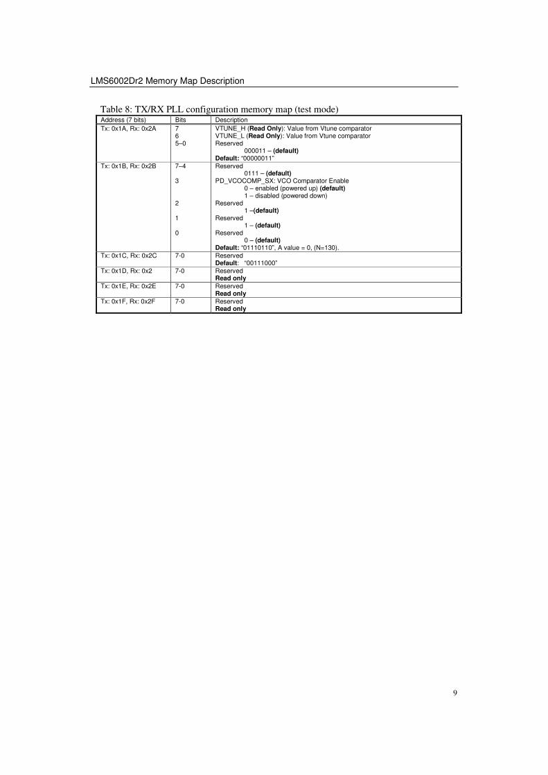
Table 8: TX/RX PLL configuration memory map (test mode) Address (7 bits) Bits Description
Tx: 0x1A, Rx: 0x2A
7 6 5–0
VTUNE_H (Read Only): Value from Vtune comparator VTUNE_L (Read Only): Value from Vtune comparator Reserved 000011 – (default) Default: “00000011”
Tx: 0x1B, Rx: 0x2B 7–4 3 2 1 0
Reserved 0111 – (default) PD_VCOCOMP_SX: VCO Comparator Enable 0 – enabled (powered up) (default) 1 – disabled (powered down) Reserved 1 –(default) Reserved 1 – (default) Reserved 0 – (default) Default: “01110110”, A value = 0, (N=130).
Tx: 0x1C, Rx: 0x2C
7-0
Reserved Default: “00111000”
Tx: 0x1D, Rx: 0x2 7-0 Reserved Read only
Tx: 0x1E, Rx: 0x2E 7-0 Reserved Read only
Tx: 0x1F, Rx: 0x2F 7-0 Reserved Read only
LMS6002 – Wide Band Multi Standard Radio Chip in 0.18um BiCMOS Programming and Calibration Guide
10
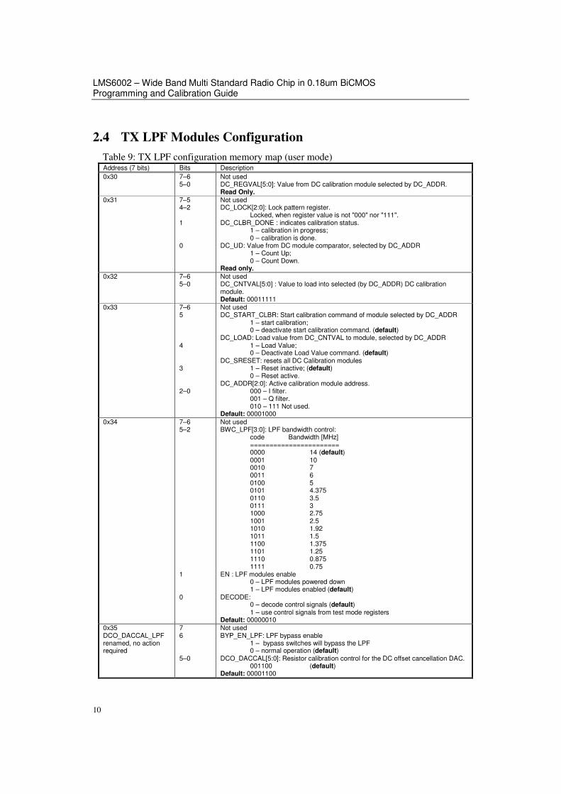
2.4 TX LPF Modules Configuration
Table 9: TX LPF configuration memory map (user mode) Address (7 bits) Bits Description
0x30 7–6 5–0
Not used DC_REGVAL[5:0]: Value from DC calibration module selected by DC_ADDR. Read Only.
0x31 7–5 4–2 1 0
Not used DC_LOCK[2:0]: Lock pattern register. Locked, when register value is not "000" nor "111". DC_CLBR_DONE : indicates calibration status. 1 – calibration in progress; 0 – calibration is done. DC_UD: Value from DC module comparator, selected by DC_ADDR 1 – Count Up; 0 – Count Down. Read only.
0x32 7–6 5–0
Not used DC_CNTVAL[5:0] : Value to load into selected (by DC_ADDR) DC calibration module. Default: 00011111
0x33 7–6 5 4 3 2–0
Not used DC_START_CLBR: Start calibration command of module selected by DC_ADDR 1 – start calibration; 0 – deactivate start calibration command. (default) DC_LOAD: Load value from DC_CNTVAL to module, selected by DC_ADDR 1 – Load Value; 0 – Deactivate Load Value command. (default) DC_SRESET: resets all DC Calibration modules 1 – Reset inactive; (default) 0 – Reset active. DC_ADDR[2:0]: Active calibration module address. 000 – I filter. 001 – Q filter. 010 – 111 Not used. Default: 00001000
0x34 7–6 5–2 1 0
Not used BWC_LPF[3:0]: LPF bandwidth control: code Bandwidth [MHz] ======================= 0000 14 (default) 0001 10 0010 7 0011 6 0100 5 0101 4.375 0110 3.5 0111 3 1000 2.75 1001 2.5 1010 1.92 1011 1.5 1100 1.375 1101 1.25 1110 0.875 1111 0.75 EN : LPF modules enable 0 – LPF modules powered down 1 – LPF modules enabled (default) DECODE: 0 – decode control signals (default) 1 – use control signals from test mode registers Default: 00000010
0x35 DCO_DACCAL_LPF renamed, no action required
7 6 5–0
Not used BYP_EN_LPF: LPF bypass enable 1 – bypass switches will bypass the LPF 0 – normal operation (default) DCO_DACCAL[5:0]: Resistor calibration control for the DC offset cancellation DAC. 001100 (default) Default: 00001100
LMS6002Dr2 Memory Map Description
11
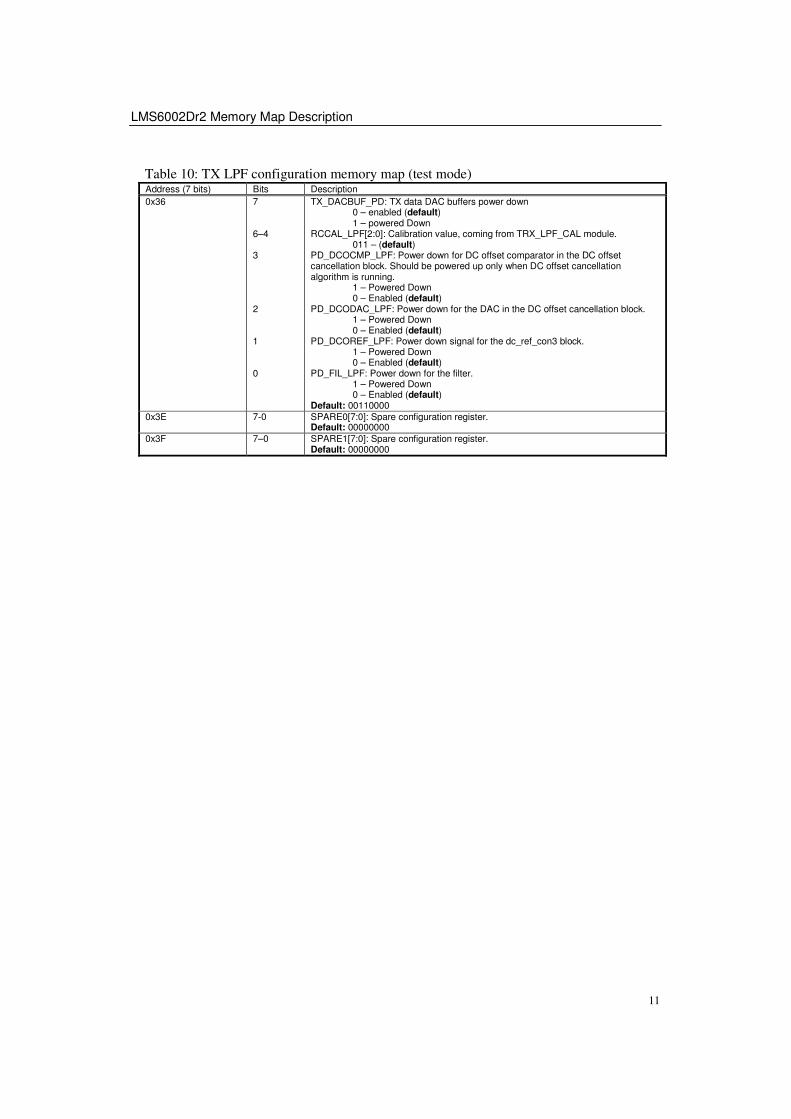
Table 10: TX LPF configuration memory map (test mode) Address (7 bits) Bits Description
0x36 7 6–4 3 2 1 0
TX_DACBUF_PD: TX data DAC buffers power down 0 – enabled (default) 1 – powered Down RCCAL_LPF[2:0]: Calibration value, coming from TRX_LPF_CAL module. 011 – (default) PD_DCOCMP_LPF: Power down for DC offset comparator in the DC offset cancellation block. Should be powered up only when DC offset cancellation algorithm is running. 1 – Powered Down 0 – Enabled (default) PD_DCODAC_LPF: Power down for the DAC in the DC offset cancellation block. 1 – Powered Down 0 – Enabled (default) PD_DCOREF_LPF: Power down signal for the dc_ref_con3 block. 1 – Powered Down 0 – Enabled (default) PD_FIL_LPF: Power down for the filter. 1 – Powered Down 0 – Enabled (default) Default: 00110000
0x3E 7-0 SPARE0[7:0]: Spare configuration register. Default: 00000000
0x3F 7–0 SPARE1[7:0]: Spare configuration register. Default: 00000000

LMS6002 – Wide Band Multi Standard Radio Chip in 0.18um BiCMOS Programming and Calibration Guide
12
2.5 RX LPF, ADC and DAC Modules Configuration
Table 11: RX LPF configuration memory map (user mode) Address (7 bits) Bits Description
0x50 7–6 5–0
Not used DC_REGVAL[5:0]: Value from DC Calibration module, selected by DC_ADDR. Read Only.
0x51 7–5 4–2 1 0
Not used DC_LOCK[2:0]: Lock pattern register. Locked, when register value is not "000" nor "111". DC_CLBR_DONE : indicates calibration status. 1 – calibration in progress; 0 – calibration is done. DC_UD: Value from DC module comparator, selected by DC_ADDR 1 – Count Up; 0 – Count Down. Read Only.
0x52 7–6 5–0
Not used DC_CNTVAL[5:0] : Value to load into selected (by DC_ADDR) DC calibration module. Default: 00011111
0x53 7–6 5 4 3 2–0
Not used DC_START_CLBR: Start calibration command on module, selected by DC_ADDR 1 – Start Calibration; 0 – Deactivate Start Calibration command. (default) DC_LOAD: Load value from DC_CNTVAL to module, selected by DC_ADDR 1 – Load Value; 0 – Deactivate Load Value command. (default) DC_SRESET: resets all DC Calibration modules 1 – Reset inactive; (default) 0 – Reset active. DC_ADDR[3:0]: Active calibration module address. 000 – I filter.(default) 001 – Q filter. 010 – 111 Not used. Default: 00001000
0x54 7–6 5–2 1 0
Not Used BWC_LPF[3:0]: LPF bandwidth control: code Bandwidth [MHz] ======================= 0000 14 (default) 0001 10 0010 7 0011 6 0100 5 0101 4.375 0110 3.5 0111 3 1000 2.75 1001 2.5 1010 1.92 1011 1.5 1100 1.375 1101 1.25 1110 0.875 1111 0.75 EN_LPF : LPF modules enable 0 – LPF modules powered down 1 – LPF modules enabled (default) DECODE: 0 – decode control signals (default) 1 – use control signals from test mode registers Default: 00000010
0x55 7 6 5–0
Not Used BYP_EN_LPF: LPF bypass enable 1 – bypass switches will bypass the LPF 0 – normal operation (default) DCO_DACCAL[5:0]: Resistor calibration control for the DC offset cancellation DAC. 001100 (default) Default: 00001100
LMS6002Dr2 Memory Map Description
13
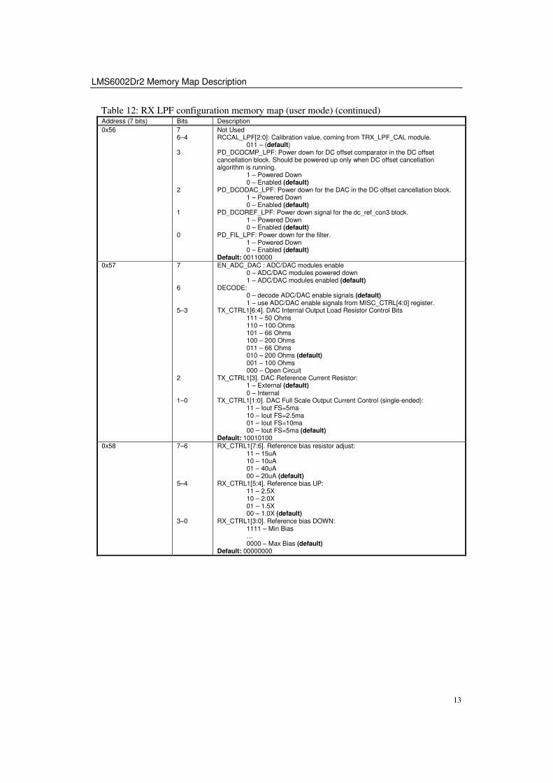
Table 12: RX LPF configuration memory map (user mode) (continued) Address (7 bits) Bits Description
0x56 7 6–4 3 2 1 0
Not Used RCCAL_LPF[2:0]: Calibration value, coming from TRX_LPF_CAL module. 011 – (default) PD_DCOCMP_LPF: Power down for DC offset comparator in the DC offset cancellation block. Should be powered up only when DC offset cancellation algorithm is running. 1 – Powered Down 0 – Enabled (default) PD_DCODAC_LPF: Power down for the DAC in the DC offset cancellation block. 1 – Powered Down 0 – Enabled (default) PD_DCOREF_LPF: Power down signal for the dc_ref_con3 block. 1 – Powered Down 0 – Enabled (default) PD_FIL_LPF: Power down for the filter. 1 – Powered Down 0 – Enabled (default) Default: 00110000
0x57 7 6 5–3 2 1–0
EN_ADC_DAC : ADC/DAC modules enable 0 – ADC/DAC modules powered down 1 – ADC/DAC modules enabled (default) DECODE: 0 – decode ADC/DAC enable signals (default) 1 – use ADC/DAC enable signals from MISC_CTRL[4:0] register. TX_CTRL1[6:4]. DAC Internal Output Load Resistor Control Bits 111 – 50 Ohms 110 – 100 Ohms 101 – 66 Ohms 100 – 200 Ohms 011 – 66 Ohms 010 – 200 Ohms (default) 001 – 100 Ohms 000 – Open Circuit TX_CTRL1[3]. DAC Reference Current Resistor: 1 – External (default) 0 – Internal TX_CTRL1[1:0]. DAC Full Scale Output Current Control (single-ended): 11 – Iout FS=5ma 10 – Iout FS=2.5ma 01 – Iout FS=10ma 00 – Iout FS=5ma (default) Default: 10010100
0x58 7–6 5–4 3–0
RX_CTRL1[7:6]. Reference bias resistor adjust: 11 – 15uA 10 – 10uA 01 – 40uA 00 – 20uA (default) RX_CTRL1[5:4]. Reference bias UP: 11 – 2.5X 10 – 2.0X 01 – 1.5X 00 – 1.0X (default) RX_CTRL1[3:0]. Reference bias DOWN: 1111 – Min Bias … 0000 – Max Bias (default) Default: 00000000
LMS6002 – Wide Band Multi Standard Radio Chip in 0.18um BiCMOS Programming and Calibration Guide
14
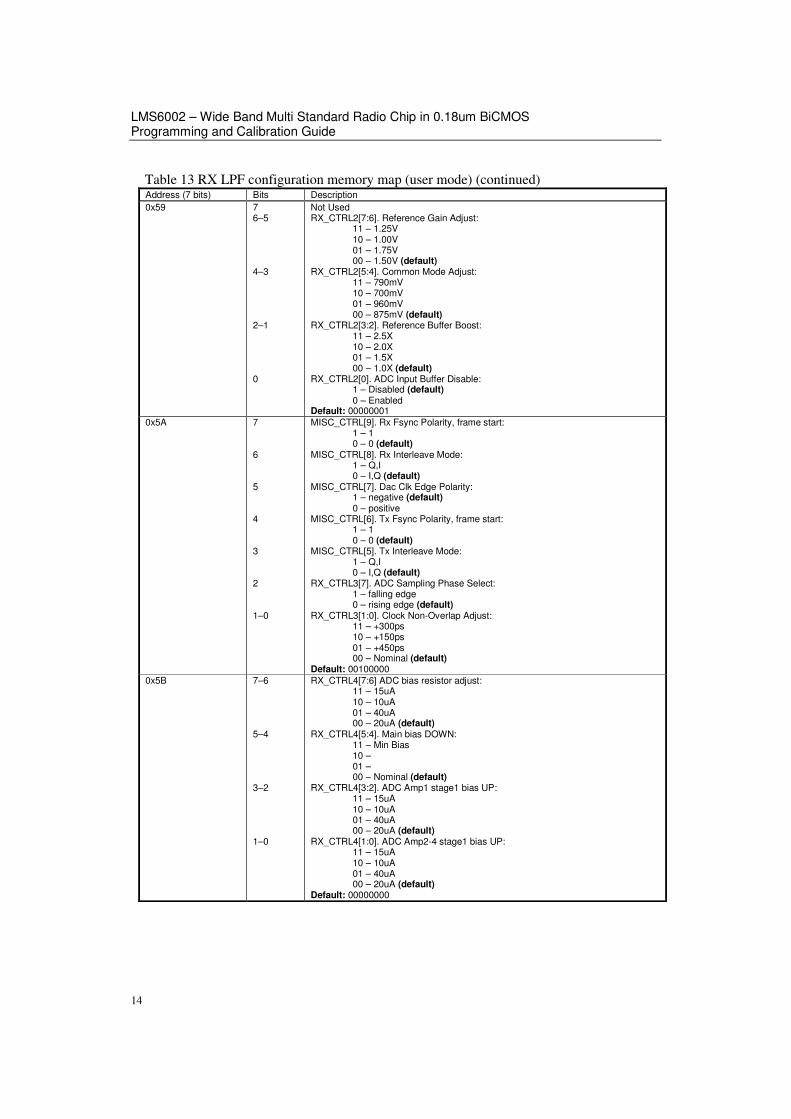
Table 13 RX LPF configuration memory map (user mode) (continued) Address (7 bits) Bits Description
0x59 7 6–5 4–3 2–1 0
Not Used RX_CTRL2[7:6]. Reference Gain Adjust: 11 – 1.25V 10 – 1.00V 01 – 1.75V 00 – 1.50V (default) RX_CTRL2[5:4]. Common Mode Adjust: 11 – 790mV 10 – 700mV 01 – 960mV 00 – 875mV (default) RX_CTRL2[3:2]. Reference Buffer Boost: 11 – 2.5X 10 – 2.0X 01 – 1.5X 00 – 1.0X (default) RX_CTRL2[0]. ADC Input Buffer Disable: 1 – Disabled (default) 0 – Enabled Default: 00000001
0x5A 7 6 5 4 3 2 1–0
MISC_CTRL[9]. Rx Fsync Polarity, frame start: 1 – 1 0 – 0 (default) MISC_CTRL[8]. Rx Interleave Mode: 1 – Q,I 0 – I,Q (default) MISC_CTRL[7]. Dac Clk Edge Polarity: 1 – negative (default) 0 – positive MISC_CTRL[6]. Tx Fsync Polarity, frame start: 1 – 1 0 – 0 (default) MISC_CTRL[5]. Tx Interleave Mode: 1 – Q,I 0 – I,Q (default) RX_CTRL3[7]. ADC Sampling Phase Select: 1 – falling edge 0 – rising edge (default) RX_CTRL3[1:0]. Clock Non-Overlap Adjust: 11 – +300ps 10 – +150ps 01 – +450ps 00 – Nominal (default) Default: 00100000
0x5B 7–6 5–4 3–2 1–0
RX_CTRL4[7:6] ADC bias resistor adjust: 11 – 15uA 10 – 10uA 01 – 40uA 00 – 20uA (default) RX_CTRL4[5:4]. Main bias DOWN: 11 – Min Bias 10 – 01 – 00 – Nominal (default) RX_CTRL4[3:2]. ADC Amp1 stage1 bias UP: 11 – 15uA 10 – 10uA 01 – 40uA 00 – 20uA (default) RX_CTRL4[1:0]. ADC Amp2-4 stage1 bias UP: 11 – 15uA 10 – 10uA 01 – 40uA 00 – 20uA (default) Default: 00000000
LMS6002Dr2 Memory Map Description
15
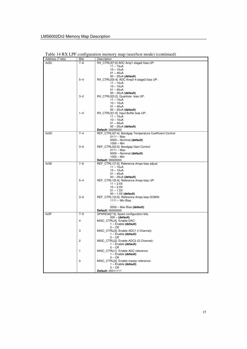
Table 14 RX LPF configuration memory map (user/test mode) (continued) Address (7 bits) Bits Description
0x5C 7–6 5–4 3–2 1–0
RX_CTRL5[7:6] ADC Amp1 stage2 bias UP: 11 – 15uA 10 – 10uA 01 – 40uA 00 – 20uA (default) RX_CTRL5[5:4]. ADC Amp2-4 stage2 bias UP: 11 – 15uA 10 – 10uA 01 – 40uA 00 – 20uA (default) RX_CTRL5[3:2]. Quantizer bias UP: 11 – 15uA 10 – 10uA 01 – 40uA 00 – 20uA (default) RX_CTRL5[1:0]. Input Buffer bias UP: 11 – 15uA 10 – 10uA 01 – 40uA 00 – 20uA (default) Default: 00000000
0x5D
7–4 3–0
REF_CTRL0[7:4]. Bandgap Temperature Coefficient Control: 0111 – Max 0000 – Nominal (default) 1000 – Min REF_CTRL0[3:0]. Bandgap Gain Control: 0111 – Max 0000 – Nominal (default) 1000 – Min Default: 00000000
0x5E
7–6 5–4 3–0
REF_CTRL1[7:6]. Reference Amps bias adjust 11 – 15uA 10 – 10uA 01 – 40uA 00 – 20uA (default) REF_CTRL1[5:4]. Reference Amps bias UP: 11 – 2.5X 10 – 2.0X 01 – 1.5X 00 – 1.0X (default) REF_CTRL1[3:0]. Reference Amps bias DOWN: 1111 – Min Bias … 0000 – Max Bias (default) Default: 00000000
0x5F 7–5 4 3 2 1 0
SPARE00[7:5]: Spare configuration bits. 000 – (default) MISC_CTRL[4]. Enable DAC: 1 – Enable (default) 0 – Off MISC_CTRL[3]. Enable ADC1 (I Channel): 1 – Enable (default) 0 – Off MISC_CTRL[2]. Enable ADC2 (Q Channel): 1 – Enable (default) 0 – Off MISC_CTRL[1]. Enable ADC reference: 1 – Enable (default) 0 – Off MISC_CTRL[0]. Enable master reference: 1 – Enable (default) 0 – Off Default: 00011111
LMS6002 – Wide Band Multi Standard Radio Chip in 0.18um BiCMOS Programming and Calibration Guide
16
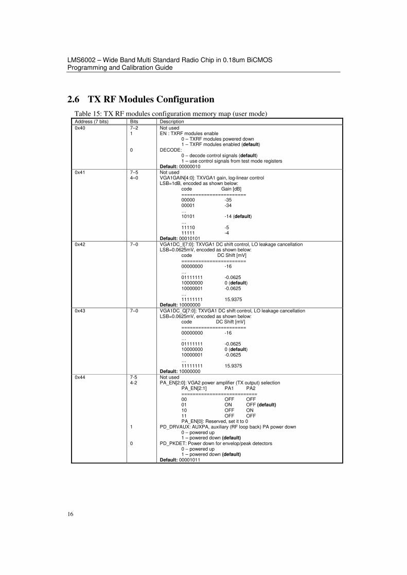
2.6 TX RF Modules Configuration
Table 15: TX RF modules configuration memory map (user mode) Address (7 bits) Bits Description
0x40 7–2 1 0
Not used EN : TXRF modules enable 0 – TXRF modules powered down 1 – TXRF modules enabled (default) DECODE: 0 – decode control signals (default) 1 – use control signals from test mode registers Default: 00000010
0x41 7–5 4–0
Not used VGA1GAIN[4:0]: TXVGA1 gain, log-linear control LSB=1dB, encoded as shown below: code Gain [dB] ======================= 00000 -35 00001 -34 … 10101 -14 (default) … 11110 -5 11111 -4 Default: 00010101
0x42 7–0 VGA1DC_I[7:0]: TXVGA1 DC shift control, LO leakage cancellation LSB=0.0625mV, encoded as shown below: code DC Shift [mV] ======================= 00000000 -16 … 01111111 -0.0625 10000000 0 (default) 10000001 -0.0625 … 11111111 15.9375 Default: 10000000
0x43 7–0 VGA1DC_Q[7:0]: TXVGA1 DC shift control, LO leakage cancellation LSB=0.0625mV, encoded as shown below: code DC Shift [mV] ======================= 00000000 -16 … 01111111 -0.0625 10000000 0 (default) 10000001 -0.0625 … 11111111 15.9375 Default: 10000000
0x44 7-5 4-2 1 0
Not used PA_EN[2:0]: VGA2 power amplifier (TX output) selection PA_EN[2:1] PA1 PA2 =========================== 00 OFF OFF 01 ON OFF (default) 10 OFF ON 11 OFF OFF PA_EN[0]: Reserved, set it to 0 PD_DRVAUX: AUXPA, auxiliary (RF loop back) PA power down 0 – powered up 1 – powered down (default) PD_PKDET: Power down for envelop/peak detectors 0 – powered up 1 – powered down (default) Default: 00001011

LMS6002Dr2 Memory Map Description
17
Table 16: TX RF modules configuration memory map (user mode) (continued) Address (7 bits) Bits Description
0x45 7-3 2-0
VGA2GAIN[4:0]: TXVGA2 gain control, log-linear control LSB=1dB, encoded as shown below: code Gain [dB] =======================
00000 0 (default) 00001 1
11001 25 ... 11111 25 ENVD[2:0]: Controls envelop/peak detector analogue MUX ENVD[1:0]: Detector select, MUX provides 00 – AUXPA envelop detector output (default) 01 – AUXPA peak detector output 10 – PA1 envelop detector output 11 – PA2 envelop detector output ENVD[2]: Selects the signal for AC coupling, MUX provides 0 – reference DC generated inside the selected detector (default) 1 – average of the selected detector output Default: 00000000
0x46 7-4 3-2 1 0
PKDBW[3:0]: Controls the bandwidth of the envelop and peak detectors 0000 – Minimum bandwidth, envelop ~1MHz, peak 30kHz (default) 1111 – Maximum bandwidth, envelop ~15MHz, peak ~300KHz LOOPBBEN[1:0]: Base band loop back switches control 00 – Switch open (default) 11 – Switch closed. FST_PKDET: Shorts the resistor in the envelop/peak detector to speed up charging for faster response. After the initial charge up, it should be disabled to achieve a LPF function. 0 – switch open, LPF function in effect (default) 1 – resistor shorted (no LPF function) FST_TXHFBIAS: Bias stage of high frequency TX part has large resistors to filter the noise. However, they create large settling time. This switch can be used to short those resistors during the initialization and then it may be needed to open it to filter the noise, in case the noise is too high. 0 – switch open (noise filtering functional) (default) 1 – resistors shorted (short settling - no noise filtering) Default: 00000000
0x47 7-4 3-0
ICT_TXLOBUF[3:0]: Controls the bias current of the LO buffer. Higher current will increase the linearity. LSB=5/6mA. 0000 – minimum current 0110 – TXMIX takes 5mA for buffer (default) 1111 – maximum current VBCAS_TXDRV[3:0]: The linearity of PAs depends on the bias at the base of the cascode npn's in the PA cells. Increasing the VBCAS will lower the base of the cascode npn. 0000 – maximum base voltage (default) 1111 – minimum base voltage Default: 01100000
0x48 7-5 4-0
Not used ICT_TXMIX[4:0]: Controls the bias current of the mixer. Higher current will increase the linearity. LSB=1mA. 00000 – 0 mA 01100 – TXMIX takes 12mA for each cell (default) 11111 – 31 mA Default: 00001100
0x49 7-5 4-0
Not used ICT_TXDRV[4:0]: Controls the bias current of the PAs. Higher current will increase the linearity. LSB=1mA. 00000 – 0 mA 01100 – PAs take 12mA for each cell (default) 11111 – 31 mA Default: 00001100
LMS6002 – Wide Band Multi Standard Radio Chip in 0.18um BiCMOS Programming and Calibration Guide
18
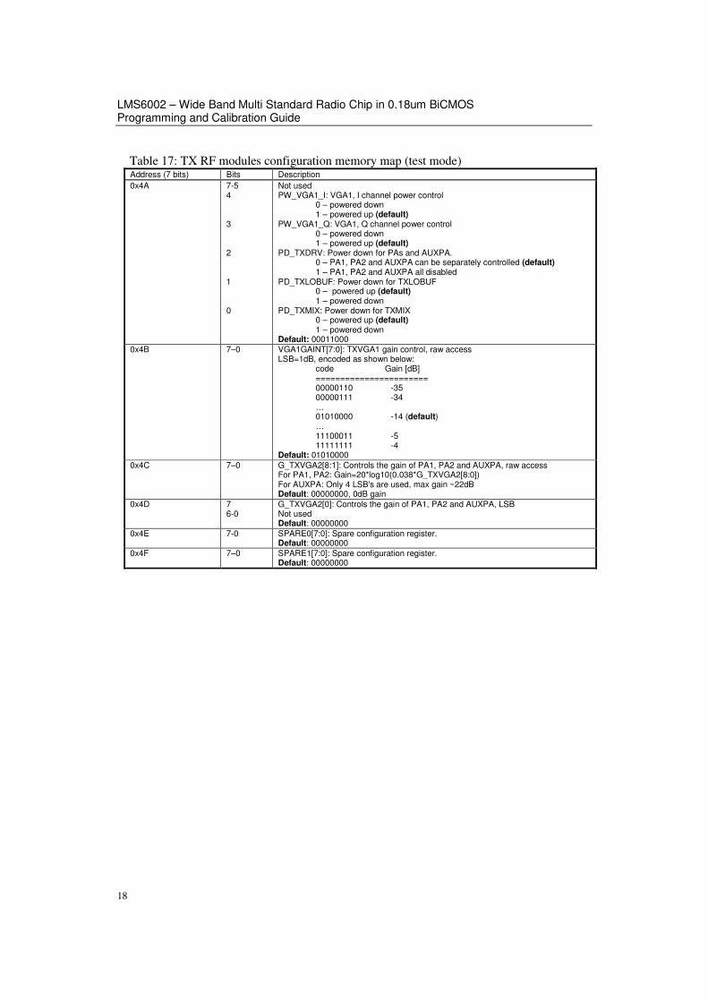
Table 17: TX RF modules configuration memory map (test mode) Address (7 bits) Bits Description
0x4A 7-5 4 3 2 1 0
Not used PW_VGA1_I: VGA1, I channel power control 0 – powered down 1 – powered up (default) PW_VGA1_Q: VGA1, Q channel power control 0 – powered down 1 – powered up (default) PD_TXDRV: Power down for PAs and AUXPA. 0 – PA1, PA2 and AUXPA can be separately controlled (default) 1 – PA1, PA2 and AUXPA all disabled PD_TXLOBUF: Power down for TXLOBUF 0 – powered up (default) 1 – powered down PD_TXMIX: Power down for TXMIX 0 – powered up (default) 1 – powered down Default: 00011000
0x4B 7–0 VGA1GAINT[7:0]: TXVGA1 gain control, raw access LSB=1dB, encoded as shown below: code Gain [dB] ======================= 00000110 -35 00000111 -34 … 01010000 -14 (default) … 11100011 -5 11111111 -4 Default: 01010000
0x4C 7–0 G_TXVGA2[8:1]: Controls the gain of PA1, PA2 and AUXPA, raw access For PA1, PA2: Gain=20*log10(0.038*G_TXVGA2[8:0]) For AUXPA: Only 4 LSB's are used, max gain ~22dB Default: 00000000, 0dB gain
0x4D 7 6-0
G_TXVGA2[0]: Controls the gain of PA1, PA2 and AUXPA, LSB Not used Default: 00000000
0x4E 7-0 SPARE0[7:0]: Spare configuration register. Default: 00000000
0x4F 7–0 SPARE1[7:0]: Spare configuration register. Default: 00000000
LMS6002Dr2 Memory Map Description
19
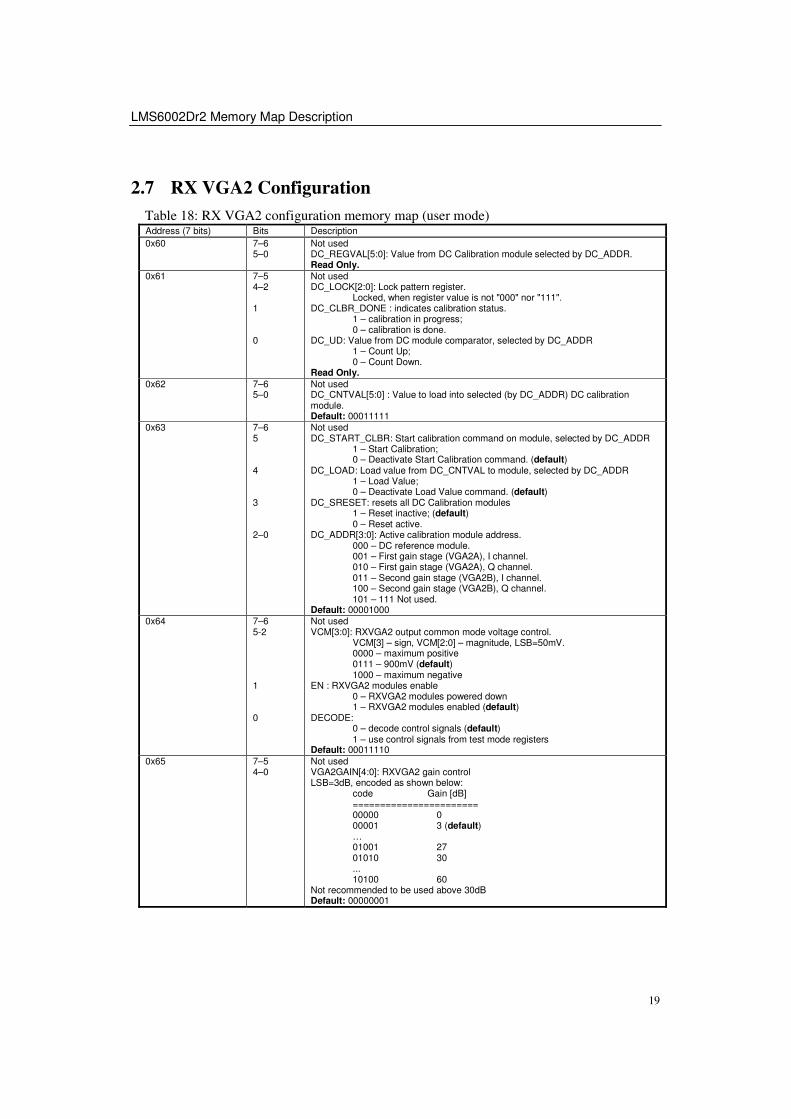
2.7 RX VGA2 Configuration
Table 18: RX VGA2 configuration memory map (user mode) Address (7 bits) Bits Description
0x60 7–6 5–0
Not used DC_REGVAL[5:0]: Value from DC Calibration module selected by DC_ADDR. Read Only.
0x61 7–5 4–2 1 0
Not used DC_LOCK[2:0]: Lock pattern register. Locked, when register value is not "000" nor "111". DC_CLBR_DONE : indicates calibration status. 1 – calibration in progress; 0 – calibration is done. DC_UD: Value from DC module comparator, selected by DC_ADDR 1 – Count Up; 0 – Count Down. Read Only.
0x62 7–6 5–0
Not used DC_CNTVAL[5:0] : Value to load into selected (by DC_ADDR) DC calibration module. Default: 00011111
0x63 7–6 5 4 3 2–0
Not used DC_START_CLBR: Start calibration command on module, selected by DC_ADDR 1 – Start Calibration; 0 – Deactivate Start Calibration command. (default) DC_LOAD: Load value from DC_CNTVAL to module, selected by DC_ADDR 1 – Load Value; 0 – Deactivate Load Value command. (default) DC_SRESET: resets all DC Calibration modules 1 – Reset inactive; (default) 0 – Reset active. DC_ADDR[3:0]: Active calibration module address. 000 – DC reference module. 001 – First gain stage (VGA2A), I channel. 010 – First gain stage (VGA2A), Q channel. 011 – Second gain stage (VGA2B), I channel. 100 – Second gain stage (VGA2B), Q channel. 101 – 111 Not used. Default: 00001000
0x64 7–6 5-2 1 0
Not used VCM[3:0]: RXVGA2 output common mode voltage control. VCM[3] – sign, VCM[2:0] – magnitude, LSB=50mV. 0000 – maximum positive 0111 – 900mV (default) 1000 – maximum negative EN : RXVGA2 modules enable 0 – RXVGA2 modules powered down 1 – RXVGA2 modules enabled (default) DECODE: 0 – decode control signals (default) 1 – use control signals from test mode registers Default: 00011110
0x65
7–5 4–0
Not used VGA2GAIN[4:0]: RXVGA2 gain control LSB=3dB, encoded as shown below: code Gain [dB] ======================= 00000 0 00001 3 (default) … 01001 27 01010 30 ... 10100 60 Not recommended to be used above 30dB Default: 00000001
LMS6002 – Wide Band Multi Standard Radio Chip in 0.18um BiCMOS Programming and Calibration Guide
20
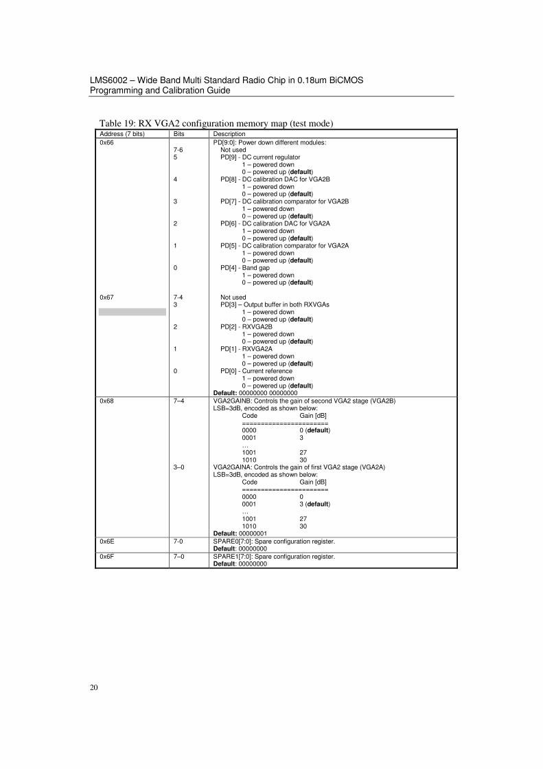
Table 19: RX VGA2 configuration memory map (test mode) Address (7 bits) Bits Description
0x66 0x67
7-6 5 4 3 2 1 0 7-4 3 2 1 0
PD[9:0]: Power down different modules: Not used PD[9] - DC current regulator 1 – powered down 0 – powered up (default) PD[8] - DC calibration DAC for VGA2B 1 – powered down 0 – powered up (default) PD[7] - DC calibration comparator for VGA2B 1 – powered down 0 – powered up (default) PD[6] - DC calibration DAC for VGA2A 1 – powered down 0 – powered up (default) PD[5] - DC calibration comparator for VGA2A 1 – powered down 0 – powered up (default) PD[4] - Band gap 1 – powered down 0 – powered up (default) Not used PD[3] – Output buffer in both RXVGAs 1 – powered down 0 – powered up (default) PD[2] - RXVGA2B 1 – powered down 0 – powered up (default) PD[1] - RXVGA2A 1 – powered down 0 – powered up (default) PD[0] - Current reference 1 – powered down 0 – powered up (default) Default: 00000000 00000000
0x68 7–4 3–0
VGA2GAINB: Controls the gain of second VGA2 stage (VGA2B) LSB=3dB, encoded as shown below: Code Gain [dB] ======================= 0000 0 (default) 0001 3 … 1001 27 1010 30 VGA2GAINA: Controls the gain of first VGA2 stage (VGA2A) LSB=3dB, encoded as shown below: Code Gain [dB] ======================= 0000 0 0001 3 (default) … 1001 27 1010 30 Default: 00000001
0x6E 7-0 SPARE0[7:0]: Spare configuration register. Default: 00000000
0x6F 7–0 SPARE1[7:0]: Spare configuration register. Default: 00000000
LMS6002Dr2 Memory Map Description
21
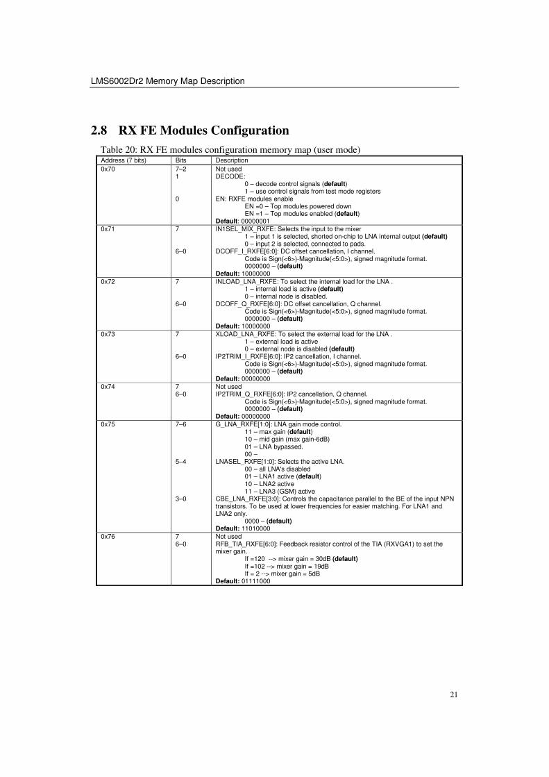
2.8 RX FE Modules Configuration
Table 20: RX FE modules configuration memory map (user mode) Address (7 bits) Bits Description
0x70
7–2 1 0
Not used DECODE: 0 – decode control signals (default) 1 – use control signals from test mode registers EN: RXFE modules enable EN =0 – Top modules powered down EN =1 – Top modules enabled (default) Default: 00000001
0x71 7 6–0
IN1SEL_MIX_RXFE: Selects the input to the mixer 1 – input 1 is selected, shorted on-chip to LNA internal output (default) 0 – input 2 is selected, connected to pads. DCOFF_I_RXFE[6:0]: DC offset cancellation, I channel. Code is Sign(<6>)-Magnitude(<5:0>), signed magnitude format. 0000000 – (default) Default: 10000000
0x72 7 6–0
INLOAD_LNA_RXFE: To select the internal load for the LNA . 1 – internal load is active (default) 0 – internal node is disabled. DCOFF_Q_RXFE[6:0]: DC offset cancellation, Q channel. Code is Sign(<6>)-Magnitude(<5:0>), signed magnitude format. 0000000 – (default) Default: 10000000
0x73 7 6–0
XLOAD_LNA_RXFE: To select the external load for the LNA . 1 – external load is active 0 – external node is disabled (default) IP2TRIM_I_RXFE[6:0]: IP2 cancellation, I channel. Code is Sign(<6>)-Magnitude(<5:0>), signed magnitude format. 0000000 – (default) Default: 00000000
0x74 7 6–0
Not used IP2TRIM_Q_RXFE[6:0]: IP2 cancellation, Q channel. Code is Sign(<6>)-Magnitude(<5:0>), signed magnitude format. 0000000 – (default) Default: 00000000
0x75 7–6 5–4 3–0
G_LNA_RXFE[1:0]: LNA gain mode control. 11 – max gain (default) 10 – mid gain (max gain-6dB) 01 – LNA bypassed. 00 – LNASEL_RXFE[1:0]: Selects the active LNA. 00 – all LNA's disabled 01 – LNA1 active (default) 10 – LNA2 active 11 – LNA3 (GSM) active CBE_LNA_RXFE[3:0]: Controls the capacitance parallel to the BE of the input NPN transistors. To be used at lower frequencies for easier matching. For LNA1 and LNA2 only. 0000 – (default) Default: 11010000
0x76 7 6–0
Not used RFB_TIA_RXFE[6:0]: Feedback resistor control of the TIA (RXVGA1) to set the mixer gain. If =120 --> mixer gain = 30dB (default) If =102 --> mixer gain = 19dB If = 2 --> mixer gain = 5dB Default: 01111000
LMS6002 – Wide Band Multi Standard Radio Chip in 0.18um BiCMOS Programming and Calibration Guide
22
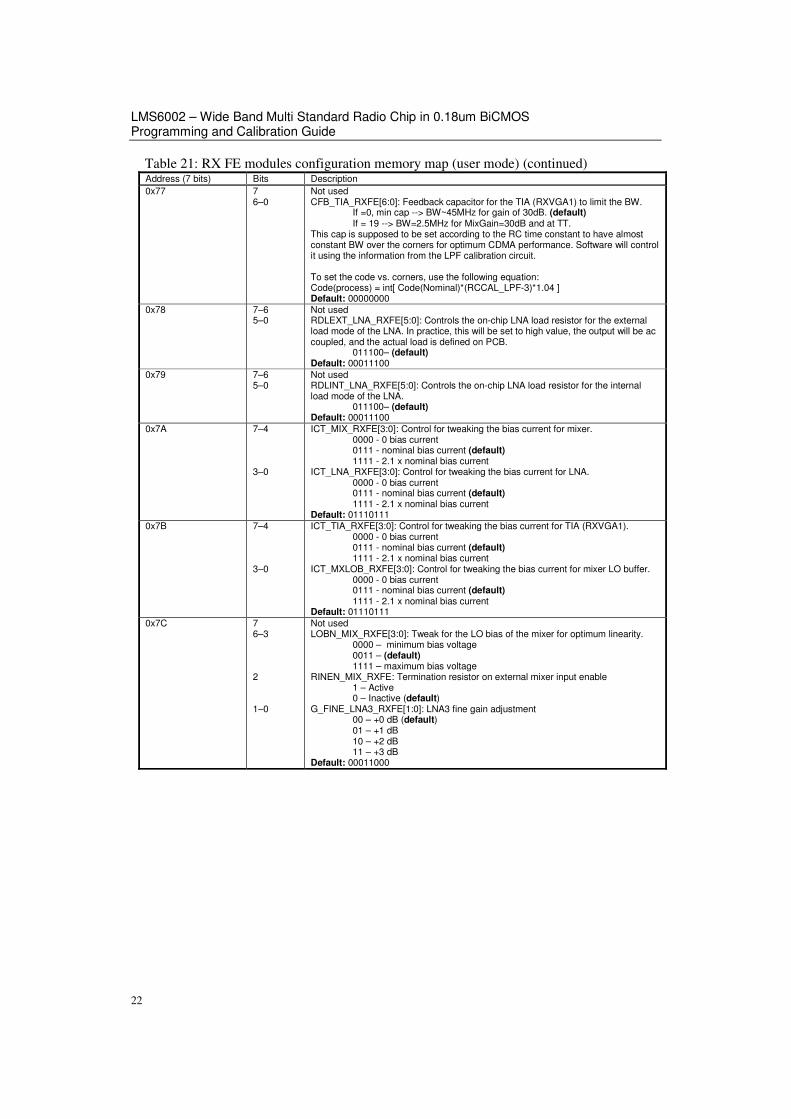
Table 21: RX FE modules configuration memory map (user mode) (continued) Address (7 bits) Bits Description
0x77 7 6–0
Not used CFB_TIA_RXFE[6:0]: Feedback capacitor for the TIA (RXVGA1) to limit the BW. If =0, min cap --> BW~45MHz for gain of 30dB. (default) If = 19 --> BW=2.5MHz for MixGain=30dB and at TT. This cap is supposed to be set according to the RC time constant to have almost constant BW over the corners for optimum CDMA performance. Software will control it using the information from the LPF calibration circuit. To set the code vs. corners, use the following equation: Code(process) = int[ Code(Nominal)*(RCCAL_LPF-3)*1.04 ] Default: 00000000
0x78 7–6 5–0
Not used RDLEXT_LNA_RXFE[5:0]: Controls the on-chip LNA load resistor for the external load mode of the LNA. In practice, this will be set to high value, the output will be ac coupled, and the actual load is defined on PCB. 011100– (default) Default: 00011100
0x79 7–6 5–0
Not used RDLINT_LNA_RXFE[5:0]: Controls the on-chip LNA load resistor for the internal load mode of the LNA. 011100– (default) Default: 00011100
0x7A 7–4 3–0
ICT_MIX_RXFE[3:0]: Control for tweaking the bias current for mixer. 0000 - 0 bias current 0111 - nominal bias current (default) 1111 - 2.1 x nominal bias current ICT_LNA_RXFE[3:0]: Control for tweaking the bias current for LNA. 0000 - 0 bias current 0111 - nominal bias current (default) 1111 - 2.1 x nominal bias current Default: 01110111
0x7B 7–4 3–0
ICT_TIA_RXFE[3:0]: Control for tweaking the bias current for TIA (RXVGA1). 0000 - 0 bias current 0111 - nominal bias current (default) 1111 - 2.1 x nominal bias current ICT_MXLOB_RXFE[3:0]: Control for tweaking the bias current for mixer LO buffer. 0000 - 0 bias current 0111 - nominal bias current (default) 1111 - 2.1 x nominal bias current Default: 01110111
0x7C 7 6–3 2 1–0
Not used LOBN_MIX_RXFE[3:0]: Tweak for the LO bias of the mixer for optimum linearity. 0000 – minimum bias voltage 0011 – (default) 1111 – maximum bias voltage RINEN_MIX_RXFE: Termination resistor on external mixer input enable 1 – Active 0 – Inactive (default) G_FINE_LNA3_RXFE[1:0]: LNA3 fine gain adjustment 00 – +0 dB (default) 01 – +1 dB 10 – +2 dB 11 – +3 dB Default: 00011000
LMS6002Dr2 Memory Map Description
23
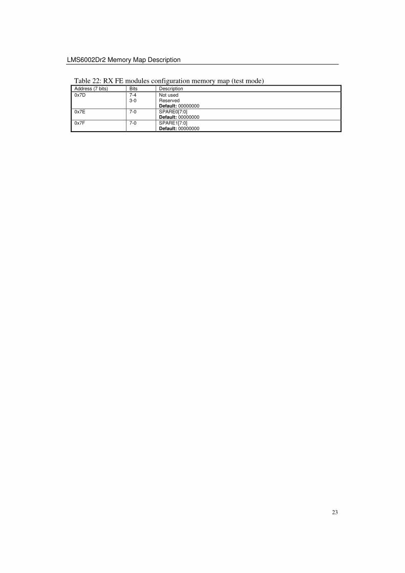
Table 22: RX FE modules configuration memory map (test mode) Address (7 bits) Bits Description
0x7D 7-4 3-0
Not used Reserved Default: 00000000
0x7E 7-0 SPARE0[7:0] Default: 00000000
0x7F 7-0 SPARE1[7:0] Default: 00000000

25
33 Control Block Diagrams
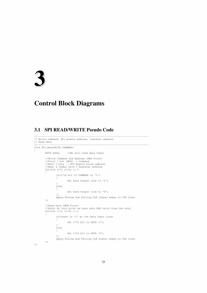
3.1 SPI READ/WRITE Pseudo Code //---------------------------------------------------------------------------- // Write command, SPI module address, register address // Read data //---------------------------------------------------------------------------- void SPI_Read(BYTE COMMAND) { BYTE DATA; //We will read data there //Write Command and Address (MSB First)
//First 1 bit (MSB) = Command //Next 3 bits = SPI memory block address //Next 4 (LSBs) bits = Register Address
for(int i=7; i>=0; i--) { if(i’th bit in COMMAND is ‘1’) { Set Data Output line to ‘1’; } else { Set Data Output line to ‘0’; }; Apply Rising and Falling CLK signal edges to CLK line; }; //Read Data (MSB First) //Note: At this point we have data MSB valid from the chip. for(int i=7; i>=0; i--) { if(there is ‘1’ at the Data Input Line) { Set i’th bit in DATA ‘1’; } else { Set i’th bit in DATA ‘0’;
}; Apply Rising and Falling CLK signal edges to CLK line; }; };
LMS6002 – Wide Band Multi Standard Radio Chip in 0.18um BiCMOS Programming and Calibration Guide
26
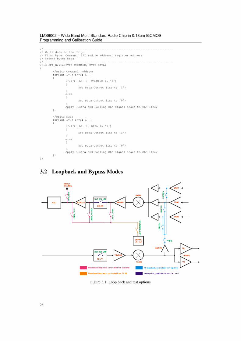
//---------------------------------------------------------------------------- // Write data to the chip: // First byte: Command, SPI module address, register address // Second byte: Data //---------------------------------------------------------------------------- void SPI_Write(BYTE COMMAND, BYTE DATA) { //Write Command, Address for(int i=7; i>=0; i--) { if(i’th bit in COMMAND is ‘1’) { Set Data Output line to ‘1’; } else { Set Data Output line to ‘0’; }; Apply Rising and Falling CLK signal edges to CLK line; }; //Write Data for(int i=7; i>=0; i--) { if(i’th bit in DATA is ‘1’) { Set Data Output line to ‘1’; } else { Set Data Output line to ‘0’; }; Apply Rising and Falling CLK signal edges to CLK line; }; };
3.2 Loopback and Bypass Modes
RXVGA1
RXLPF
RXVGA2
RXMIX
LNA2
LNA1
LNA3
TXVGA1
TXLPF
TXMIX
BYP_EN_LPF
BYP_EN_LPF
LB
EN
_O
PIN
LB
EN
_V
GA
2IN
LB
EN
_L
PF
IN
LB
RF
EN
LB
RF
EN
LB
RF
EN
Base band loop back, controlled from top level RF loop back, controlled from top level
Test option, controlled from TX/RX LPF
ENV/PKDETECT
AUX PA
ADC
RXOUTChip Pins
RX
OU
TS
W
PD[0]
Base band loop back, controlled from TX RF
LO
OP
BB
EN
[1:0
]
PA1
PA2
TXVGA2
Figure 3.1: Loop back and test options

Control Block Diagrams
27
3.3 Envelop and Pick Detector Multiplexer
TXVGA2
TXOUT1
TXOUT2
PK
DE
TMUX
To ATP pinand BB loopback
ENVD[1:0]
AUX PA
PA1
PA2
PK
DE
T
PK
DE
T
EN
VD
ET
To RF loopback
Figure 3.2: Envelop/pick detector analogue MUX
3.4 TX/RX PLL
The frequency setting for both TX and RX PLLs is the same as described here. TX PLL SPI registers are at x001xxxx and TX PLL registers are at x010xxxx. To configure the PLL there are a number of variables which need to be set.
• Integer and fractional part of the divider
• FRANGE value
• VCO CAP, charge pump current (Icp) and charge pump offset current (Ioff) This assumes the given loop filter value with a loop BW of 50kHz is used.
LMS6002 – Wide Band Multi Standard Radio Chip in 0.18um BiCMOS Programming and Calibration Guide
28
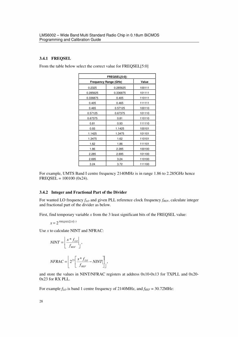
3.4.1 FREQSEL
From the table below select the correct value for FREQSEL[5:0]
FREQSEL[5:0]:
Frequency Range (GHz) Value
0.2325 0.285625 100111
0.285625 0.336875 101111
0.336875 0.405 110111
0.405 0.465 111111
0.465 0.57125 100110
0.57125 0.67375 101110
0.67375 0.81 110110
0.81 0.93 111110
0.93 1.1425 100101
1.1425 1.3475 101101
1.3475 1.62 110101
1.62 1.86 111101
1.86 2.285 100100
2.285 2.695 101100
2.695 3.24 110100
3.24 3.72 111100
For example, UMTS Band I centre frequency 2140MHz is in range 1.86 to 2.285GHz hence FREQSEL = 100100 (0x24).
3.4.2 Integer and Fractional Part of the Divider
For wanted LO frequency fLO and given PLL reference clock frequency fREF, calculate integer and fractional part of the divider as below. First, find temporary variable x from the 3 least significant bits of the FREQSEL value:
[ ] 30:22 −= FREQSELx
Use x to calculate NINT and NFRAC:
=
REF
LO
f
fxNINT
*,
−= NINT
f
fxNFRAC
REF
LO*223 ,
and store the values in NINT/NFRAC registers at address 0x10-0x13 for TXPLL and 0x20-0x23 for RX PLL. For example fLO is band 1 centre frequency of 2140MHz, and fREF = 30.72MHz:
Control Block Diagrams
29
[ ] [ ] 4401000:2,1001000:5 ==== xFREQSELFREQSEL
[ ] 2222 13430:2 ==== −−FREQSELx
13972.30
2140*2*=
=
=
REF
LO
f
fxNINT
270882113972.30
2140*22
*2 2323 =
−=
−= NINT
f
fxNFRAC
REF
LO
3.4.3 VCO Capacitor, Icp and Ioff Selection
For the PLL loop filter implemented on both evaluation and reference LMS6002D boards, loop bandwidth of 50kHz and optimum PLL phase noise performance, the following charge pump current setup is recommended:
• Charge pump current Icp=1200uA (default) • Charge pump current offset up Ioff up = 30uA.
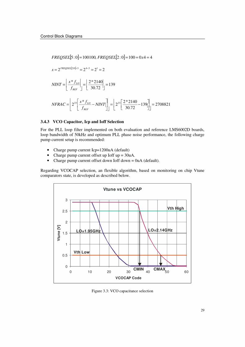
• Charge pump current offset down Ioff down = 0uA (default). Regarding VCOCAP selection, an flexible algorithm, based on monitoring on chip Vtune comparators state, is developed as described below.
Vtune vs VCOCAP
0
0.5
1
1.5
2
2.5
3
0 10 20 30 40 50 60
VCOCAP Code
Vtu
ne
[V]
Vth High
Vth Low
LO=1.95GHz LO=2.14GHz
CMIN CMAX
Figure 3.3: VCO capacitance selection
LMS6002 – Wide Band Multi Standard Radio Chip in 0.18um BiCMOS Programming and Calibration Guide
30
Figure 3.3 shows typical measured Vtune variation with the VCOCAP codes for the two target LO frequencies, 1.95GHz and 2.14GHz. Obviously, Vtune is changing from 2.9V down to 0V. However, PLL lock is guarantied only when Vtune is in the range 0.5V-2.5V. Also, for the best phase noise performance, Vtune should be kept around the middle of the range i.e. 1.5V. There are two on chip Vtune comparators per PLL as shown in Figure 3.4. Their threshold voltages are set to Vth Low=0.5V and Vth High=2.5V. The state of the comparators can be obtained by powering them up (register 0x1B for TXPLL or 0x2B for RXPLL, bit 3) and reading the register 0x1A for TXPPLL or 0x2A for RXPLL, bits 7-6. True table is given below.
VTUNE_H VTUNE_L Status
0 0 OK, Vtune in range
1 0 Vtune is high (> 2.5V), PLL lock not guaranteed.
0 1 Vtune is Low (< 0.5V), PLL lock not guaranteed.
1 1 Not possible, check SPI connections. These can be used to choose VCOCAP code. All we need to find is the code CMIN when comparators change the state from “10” to “00” and the code CMAX when the comparators change the state from “00” to “01”. Optimum VCOCAP code is then the middle one between CMIN and CMAX. For LO=2.4GHz, this is illustrated in Figure 3.3. In this case, optimum code is around 41. The algorithm is summarised as below. 1. Select correct FREQSEL as explained in section 3.4.1. 2. Set target LO frequency (NINT, NFRAC) as explained in section 3.4.2. 3. Sweep VCOCAP codes from 0-63. Monitor the state of Vtune comparators.
3.a. Record the code CMIN when Vtune comparators state changes from "10" to "00" (PLL enters 'in range' state). 3.b. Record the code CMAX when Vtune comparators state changes from "00" to "01" (PLL leaves 'in range' state). 3.c. Select the middle code between CMIN and CMAX ( C=(CMIN+CMAX)/2 ).
Note that faster search algorithm (replacement for step 3 above) can be implemented as shown in Section 4.6. Once the PLL is set, Vtune comparators can also be used as lock (in range) indication.
Control Block Diagrams
31
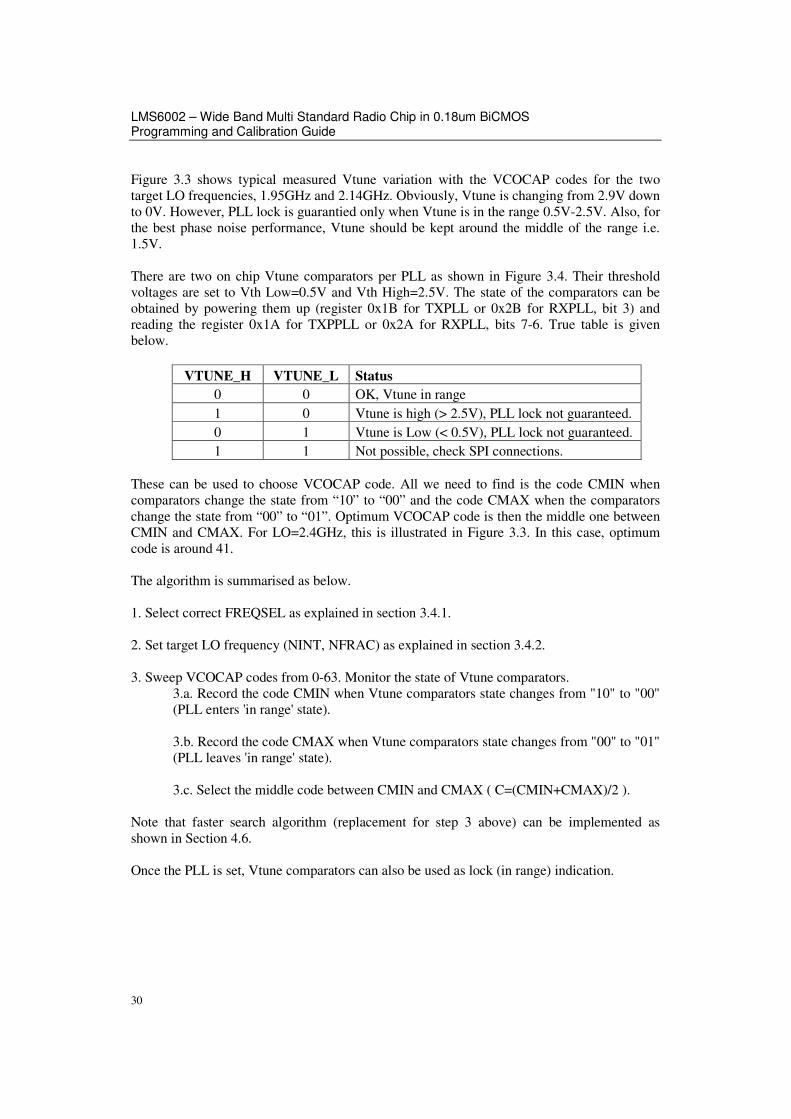
3.4.4 PLL Control
PFD
/N
LPF
VCOCHP
External
Σ∆NINT, NFRAC DITHEN, DITHN
/M
ICHPOFFUP
OFFDOWN
VCOCAP
FREQSEL
LOBUF1
LOBUF2
LOBUF3
Do not existin TX PLL
SELOUT
To
SP
I
+
-
+
-
VTUNE_L
VTUNE_H
VCOREG
3.3V 1.8V
BYPVCOREGPDVCOREGFSTVCOBGVOVCOREG
PLLCLK
EN_PFD_UP
PD_VCOCOMP_SX
Figure 3.4: PLL control
LMS6002 – Wide Band Multi Standard Radio Chip in 0.18um BiCMOS Programming and Calibration Guide
32
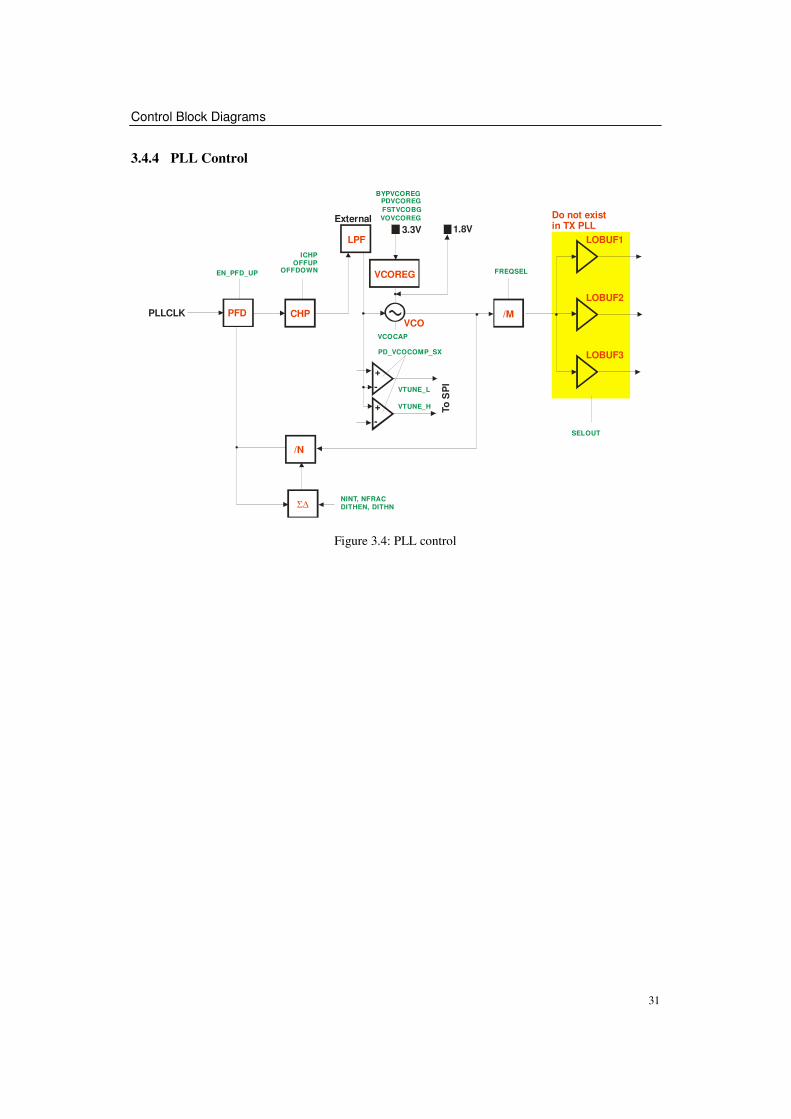
3.5 TX/RX LPF
DACBUF
LPFIin Iout
Control
TX_DACBUF_PD
DCO ComparatorDCO
DAC
DACBUF
LPFQin Qout
TX_DACBUF_PD
DCO DAC
BYP_EN_LPF
BYP_EN_LPF
Do
no
t ex
ist
in R
XL
PF
DC
O_D
AC
CA
LP
D_D
CO
DA
C_
LP
F
PD
_D
CO
CM
P_L
PF
Implemented in SPI
BWC_LPFRCCAL_LPFPD_FIL_LPF
BWC_LPFRCCAL_LPFPD_FIL_LPF
DCO Comparator
Figure 3.5: TX/RX LPF control
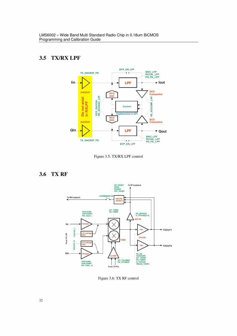
3.6 TX RF
TXVGA1
TXMIX
ENV/PKDETECT
AUX PA
LOOPBBEN[1:0]To BB loopback
PA1
PA2
TXVGA2
To RF loopback
LO LeakageDAC
TXVGA1
LO LeakageDAC
LO BUF
From TX PLL
Fro
m T
X L
PF
Iin
Qin
TXOUT1
TXOUT2
VGA1GAINVGA1GAINTPW_VGA1_Q
VGA1GAINVGA1GAINTPW_VGA1_I
VG
A1D
C_I
VG
A1
DC
_Q
PA_ENVGA2GAINICT_TXDRVPD_TXDRVG_TXVGA2VBCAS_TXDRV
PD_DRVAUXG_TXVGA2[3:0]
PD_PKDETENVDPKDBWFST_PKDET
ICT_TXLOBUFPD_TXLOBUF
ICT_TXMIXPD_TXMIX
Figure 3.6: TX RF control

Control Block Diagrams
33
3.7 RX VGA2
RXVGA2AIin
Control
DCO ComparatorDCO
DAC
Qin
DCO DAC
PD
[6]
PD
[5]
Implemented in SPI
VGA2GAINPD[1]VGA2GAINA
DCO Comparator
RXVGA2A
VGA2GAINPD[1]VGA2GAINA
RXVGA2B Iout
DCO ComparatorDCO
DAC
DCO DAC
PD
[8]
PD
[7]
Implemented in SPI
VGA2GAINPD[2]VGA2GAINB
DCO Comparator
RXVGA2B
VGA2GAINPD[2]VGA2GAINB
OutputBuffer
PD[3]
Qout
OutputBuffer
PD[3]
DCOREF
Control
ComparatorPROG RES
PD
[9]
PD[9]
PD[9]
PD[3]
Implemented in SPI
BIAS
PD[0]VCM
Control
Figure 3.7: RXVGA2 control
LMS6002 – Wide Band Multi Standard Radio Chip in 0.18um BiCMOS Programming and Calibration Guide
34
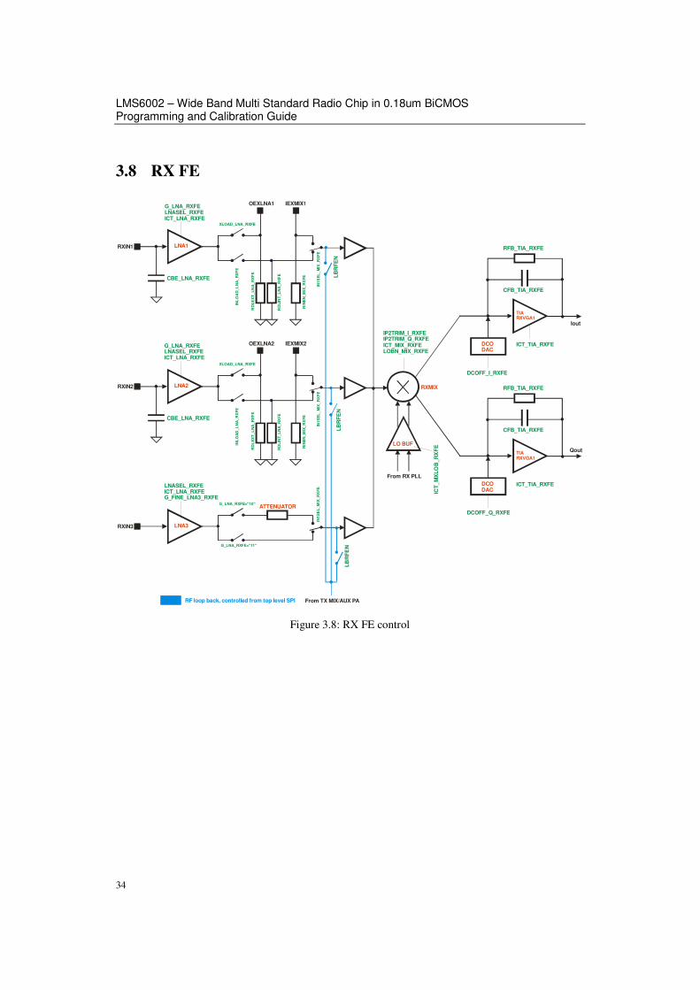
3.8 RX FE
RXMIX
LNA1
RF loop back, controlled from top level SPI
RXIN1
OEXLNA1 IEXMIX1
IN1
SE
L_
MIX
_R
XF
E
INL
OA
D_
LN
A_
RX
FE
XLOAD_LNA_RXFE
G_LNA_RXFELNASEL_RXFEICT_LNA_RXFE
CBE_LNA_RXFE
RD
LE
XT
_L
NA
_R
XF
E
RD
LIN
T_L
NA
_R
XF
E
RIN
EN
_M
IX_
RX
FE
LNA2RXIN2
OEXLNA2 IEXMIX2
IN1S
EL
_M
IX_
RX
FE
INL
OA
D_
LN
A_R
XF
E
XLOAD_LNA_RXFE
G_LNA_RXFELNASEL_RXFEICT_LNA_RXFE
CBE_LNA_RXFE
RD
LE
XT
_L
NA
_R
XF
E
RD
LIN
T_
LN
A_
RX
FE
RIN
EN
_M
IX_
RX
FE
LNA3RXIN3
IN1
SE
L_M
IX_R
XF
E
G_LNA_RXFE="11"
G_LNA_RXFE="10"
LNASEL_RXFEICT_LNA_RXFEG_FINE_LNA3_RXFE
ATTENUATOR
LB
RF
EN
LB
RF
EN
LB
RF
EN
From TX MIX/AUX PA
LO BUF
From RX PLL
ICT
_M
XL
OB
_R
XF
E
TIARXVGA1
DCODAC
DCOFF_Q_RXFE
RFB_TIA_RXFE
CFB_TIA_RXFE
Qout
ICT_TIA_RXFE
TIARXVGA1
DCODAC
DCOFF_I_RXFE
RFB_TIA_RXFE
CFB_TIA_RXFE
Iout
ICT_TIA_RXFE
IP2TRIM_I_RXFEIP2TRIM_Q_RXFEICT_MIX_RXFELOBN_MIX_RXFE
Figure 3.8: RX FE control
35
44 Calibration Flow Charts
LMS6002 – Wide Band Multi Standard Radio Chip in 0.18um BiCMOS Programming and Calibration Guide
36
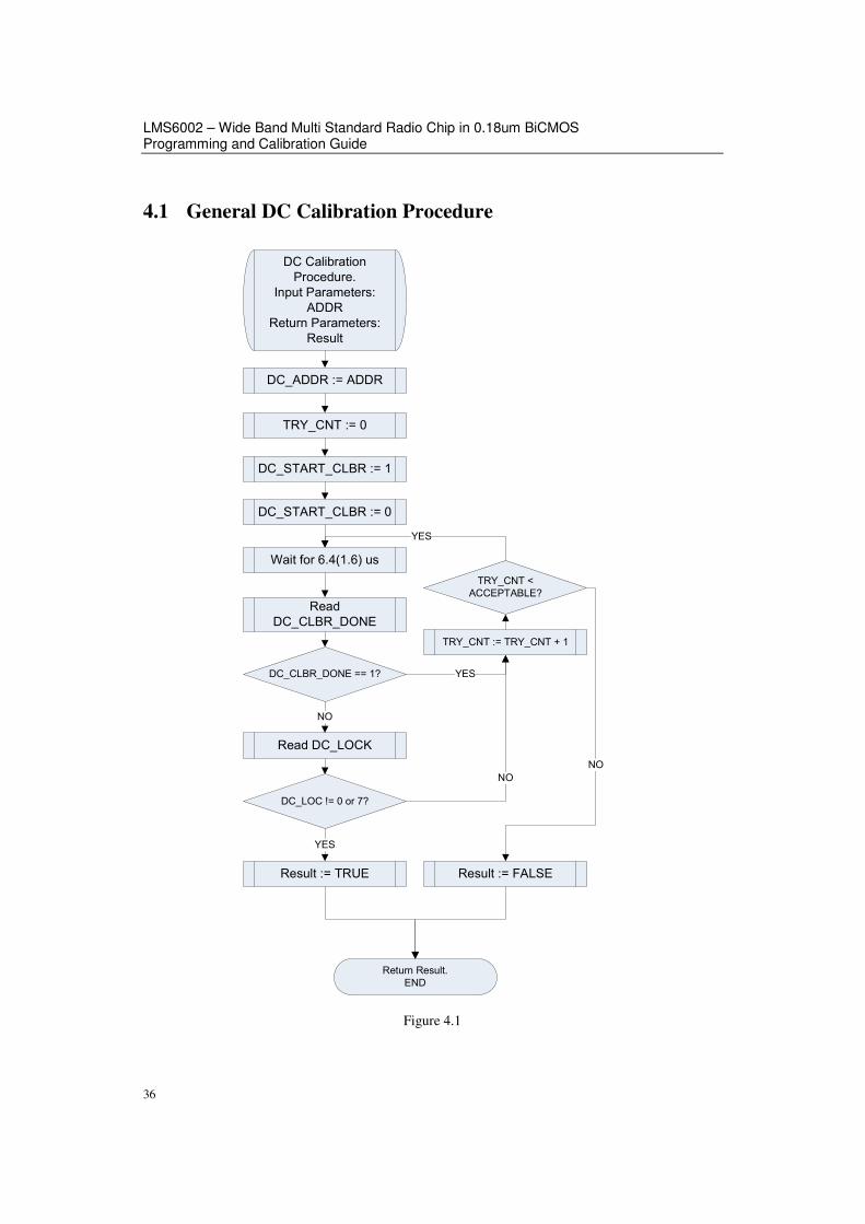
4.1 General DC Calibration Procedure
DC Calibration Procedure.
Input Parameters: ADDR
Return Parameters:Result
DC_ADDR := ADDR
DC_START_CLBR := 1
DC_START_CLBR := 0
Wait for 6.4(1.6) us
Read DC_CLBR_DONE
DC_CLBR_DONE == 1?
Read DC_LOCK
DC_LOC != 0 or 7?
Result := TRUE Result := FALSE
Return Result.END
TRY_CNT := 0
TRY_CNT := TRY_CNT + 1
YES
NO
TRY_CNT < ACCEPTABLE?
NO
YES
YES
NO
Figure 4.1
Calibration Flow Charts
37
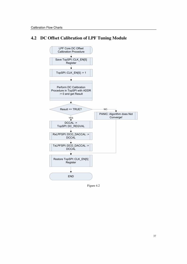
4.2 DC Offset Calibration of LPF Tuning Module
LPF Core DC Offset Calibration Procedure
Perform DC Calibration Procedure in TopSPI with ADDR
:= 0 and get Result
Result == TRUE?
DCCAL := TopSPI::DC_REGVAL
TopSPI::CLK_EN[5] := 1
Save TopSPI::CLK_EN[5] Register
RxLPFSPI::DCO_DACCAL := DCCAL
TxLPFSPI::DCO_DACCAL := DCCAL
Restore TopSPI::CLK_EN[5] Register
END
YES
PANIC: Algorithm does Not Converge!
NO
Figure 4.2
LMS6002 – Wide Band Multi Standard Radio Chip in 0.18um BiCMOS Programming and Calibration Guide
38
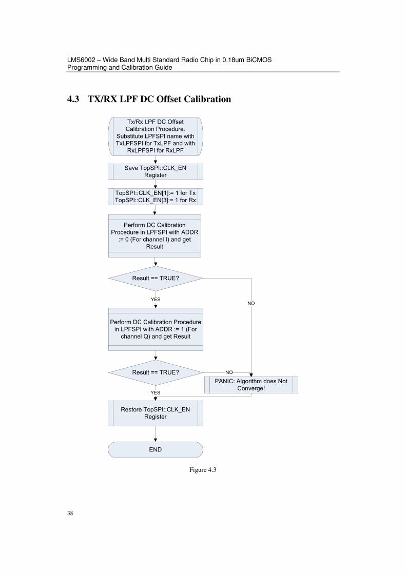
4.3 TX/RX LPF DC Offset Calibration
Tx/Rx LPF DC Offset Calibration Procedure.
Substitute LPFSPI name with TxLPFSPI for TxLPF and with
RxLPFSPI for RxLPF
Perform DC Calibration Procedure in LPFSPI with ADDR
:= 0 (For channel I) and get Result
Result == TRUE?
TopSPI::CLK_EN[1]:= 1 for TxTopSPI::CLK_EN[3]:= 1 for Rx
Save TopSPI::CLK_EN Register
Restore TopSPI::CLK_EN Register
END
YES
PANIC: Algorithm does Not Converge!
NO
Perform DC Calibration Procedure in LPFSPI with ADDR := 1 (For
channel Q) and get Result
Result == TRUE?
YES
NO
Figure 4.3
Calibration Flow Charts
39
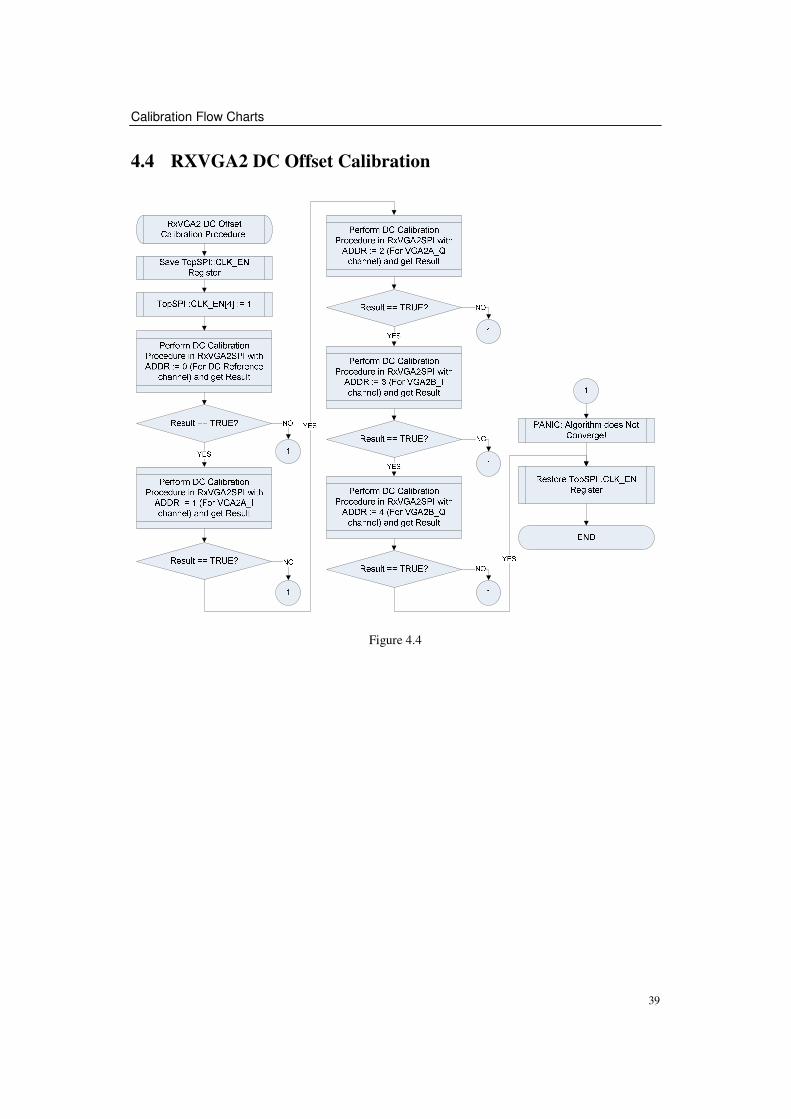
4.4 RXVGA2 DC Offset Calibration
Figure 4.4
LMS6002 – Wide Band Multi Standard Radio Chip in 0.18um BiCMOS Programming and Calibration Guide
40
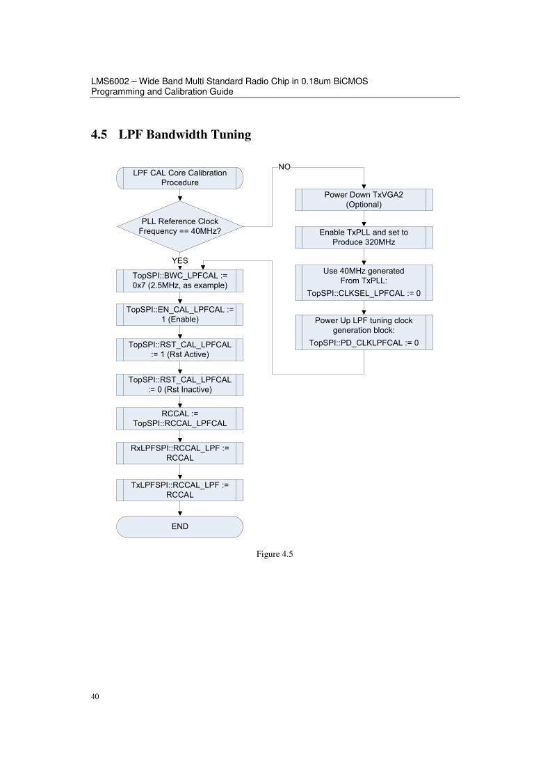
4.5 LPF Bandwidth Tuning
LPF CAL Core Calibration Procedure
TopSPI::BWC_LPFCAL := 0x7 (2.5MHz, as example)
TopSPI::EN_CAL_LPFCAL := 1 (Enable)
TopSPI::RST_CAL_LPFCAL := 1 (Rst Active)
TopSPI::RST_CAL_LPFCAL := 0 (Rst Inactive)
RCCAL := TopSPI::RCCAL_LPFCAL
RxLPFSPI::RCCAL_LPF := RCCAL
TxLPFSPI::RCCAL_LPF := RCCAL
END
PLL Reference ClockFrequency == 40MHz?
YESUse 40MHz generated
From TxPLL:TopSPI::CLKSEL_LPFCAL := 0
Power Up LPF tuning clock generation block:
TopSPI::PD_CLKLPFCAL := 0
NO
Enable TxPLL and set toProduce 320MHz
Power Down TxVGA2(Optional)
Figure 4.5
Calibration Flow Charts
41
4.6 VCOCAP Code Selection Algorithm
Figure 4.6
4.7 Auto Calibration Summary
The following is recommended auto calibration sequence.
1. DC offset cancellation of the LPF tuning module, Figure 4.2. 2. LPF bandwidth tuning, Figure 4.5. 3. DC offset cancellation of the TXLPF, Figure 4.3. 4. DC offset cancellation of the RXLPF, Figure 4.3. 5. DC offset cancellation of the RXVGA2, Figure 4.4.
Please note, while executing DC calibration procedures, no TX/RX inputs should be applied.
LMS6002 – Wide Band Multi Standard Radio Chip in 0.18um BiCMOS Programming and Calibration Guide
42
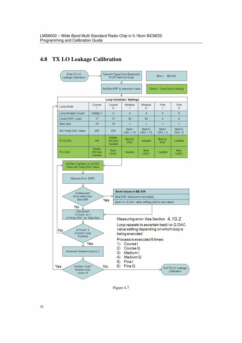
4.8 TX LO Leakage Calibration
4.10.2
Figure 4.7
Calibration Flow Charts
43
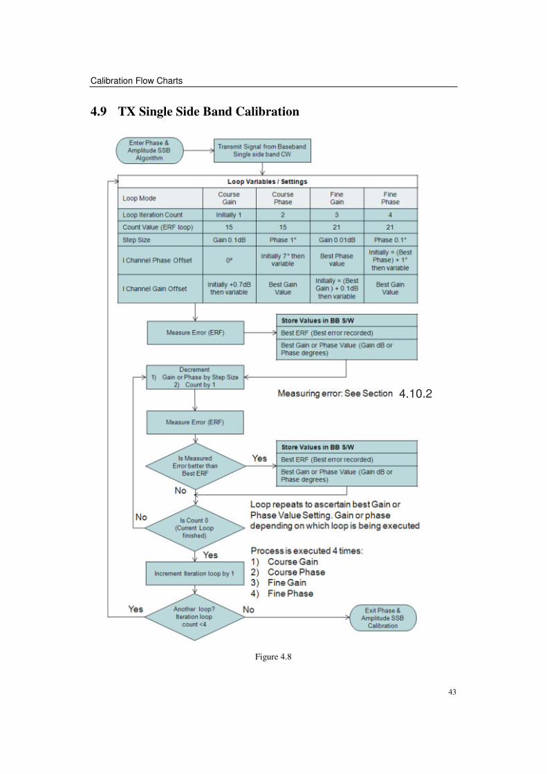
4.9 TX Single Side Band Calibration
4.10.2
Figure 4.8
LMS6002 – Wide Band Multi Standard Radio Chip in 0.18um BiCMOS Programming and Calibration Guide
44
4.10 Correction and Measurement Functions Implemented in BB
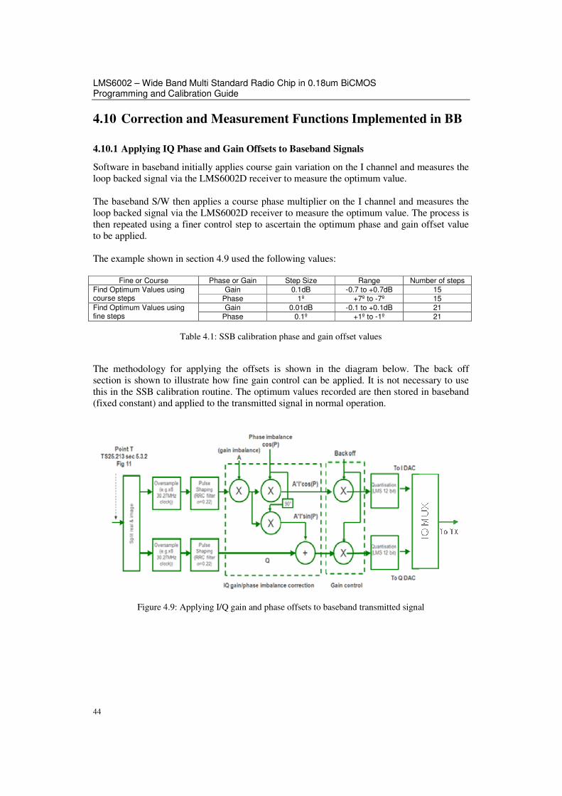
4.10.1 Applying IQ Phase and Gain Offsets to Baseband Signals
Software in baseband initially applies course gain variation on the I channel and measures the loop backed signal via the LMS6002D receiver to measure the optimum value. The baseband S/W then applies a course phase multiplier on the I channel and measures the loop backed signal via the LMS6002D receiver to measure the optimum value. The process is then repeated using a finer control step to ascertain the optimum phase and gain offset value to be applied. The example shown in section 4.9 used the following values:
Fine or Course Phase or Gain Step Size Range Number of steps Gain 0.1dB -0.7 to +0.7dB 15 Find Optimum Values using
course steps Phase 1º +7º to -7º 15 Gain 0.01dB -0.1 to +0.1dB 21 Find Optimum Values using
fine steps Phase 0.1º +1º to -1º 21
Table 4.1: SSB calibration phase and gain offset values
The methodology for applying the offsets is shown in the diagram below. The back off section is shown to illustrate how fine gain control can be applied. It is not necessary to use this in the SSB calibration routine. The optimum values recorded are then stored in baseband (fixed constant) and applied to the transmitted signal in normal operation.
Figure 4.9: Applying I/Q gain and phase offsets to baseband transmitted signal
Calibration Flow Charts
45
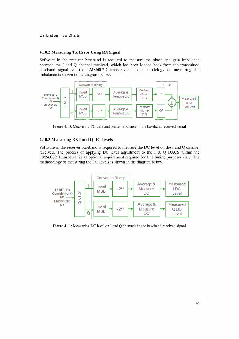
4.10.2 Measuring TX Error Using RX Signal
Software in the receiver baseband is required to measure the phase and gain imbalance between the I and Q channel received, which has been looped back from the transmitted baseband signal via the LMS6002D transceiver. The methodology of measuring the imbalance is shown in the diagram below.
Figure 4.10: Measuring I/Q gain and phase imbalance in the baseband received signal
4.10.3 Measuring RX I and Q DC Levels
Software in the receiver baseband is required to measure the DC level on the I and Q channel received. The process of applying DC level adjustment to the I & Q DACS within the LMS6002 Transceiver is an optional requirement required for fine tuning purposes only. The methodology of measuring the DC levels is shown in the diagram below.
Figure 4.11: Measuring DC level on I and Q channels in the baseband received signal


![Party Band pianoman Chip Bricker, and the Hooks … · Farewell Party Band, Nashville, TN 05/30 Bluegrass Festival On The Plains, Auburn, AL March/April Z X Y ] Volume \ X ... Party](https://img.pdfslide.us/doc/110x75/5b80e6c77f8b9af7088e652e/party-band-pianoman-chip-bricker-and-the-hooks-farewell-party-band-nashville.jpg)