Embed Size (px)
Citation preview
ECE 6450 - Dr. Alan DoolittleGeorgia Tech
Lecture 8
Photoresists and Non-optical Lithography
Reading:
Chapters 8 and 9 and notes derived from a HIGHLY recommended book by Chris Mack, “Fundamental
Principles of Optical Lithography”. Any serious student interested in a career in the semiconductor industry or lithography should consider this book as a must read.
ECE 6450 - Dr. Alan DoolittleGeorgia Tech
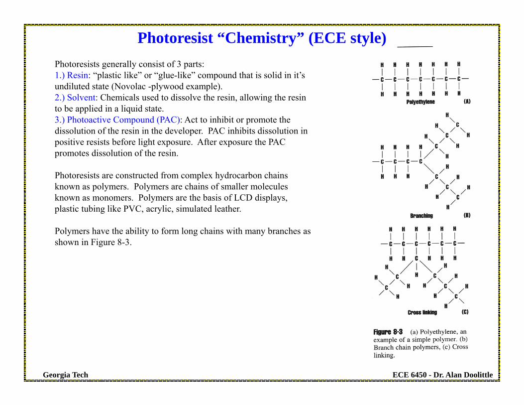
Photoresists generally consist of 3 parts:1.) Resin: “plastic like” or “glue-like” compound that is solid in it’s undiluted state (Novolac -plywood example).2.) Solvent: Chemicals used to dissolve the resin, allowing the resin to be applied in a liquid state.3.) Photoactive Compound (PAC): Act to inhibit or promote the dissolution of the resin in the developer. PAC inhibits dissolution in positive resists before light exposure. After exposure the PAC promotes dissolution of the resin.
Photoresists are constructed from complex hydrocarbon chains known as polymers. Polymers are chains of smaller molecules known as monomers. Polymers are the basis of LCD displays, plastic tubing like PVC, acrylic, simulated leather.
Polymers have the ability to form long chains with many branches as shown in Figure 8-3.
Photoresist “Chemistry” (ECE style)
ECE 6450 - Dr. Alan DoolittleGeorgia Tech
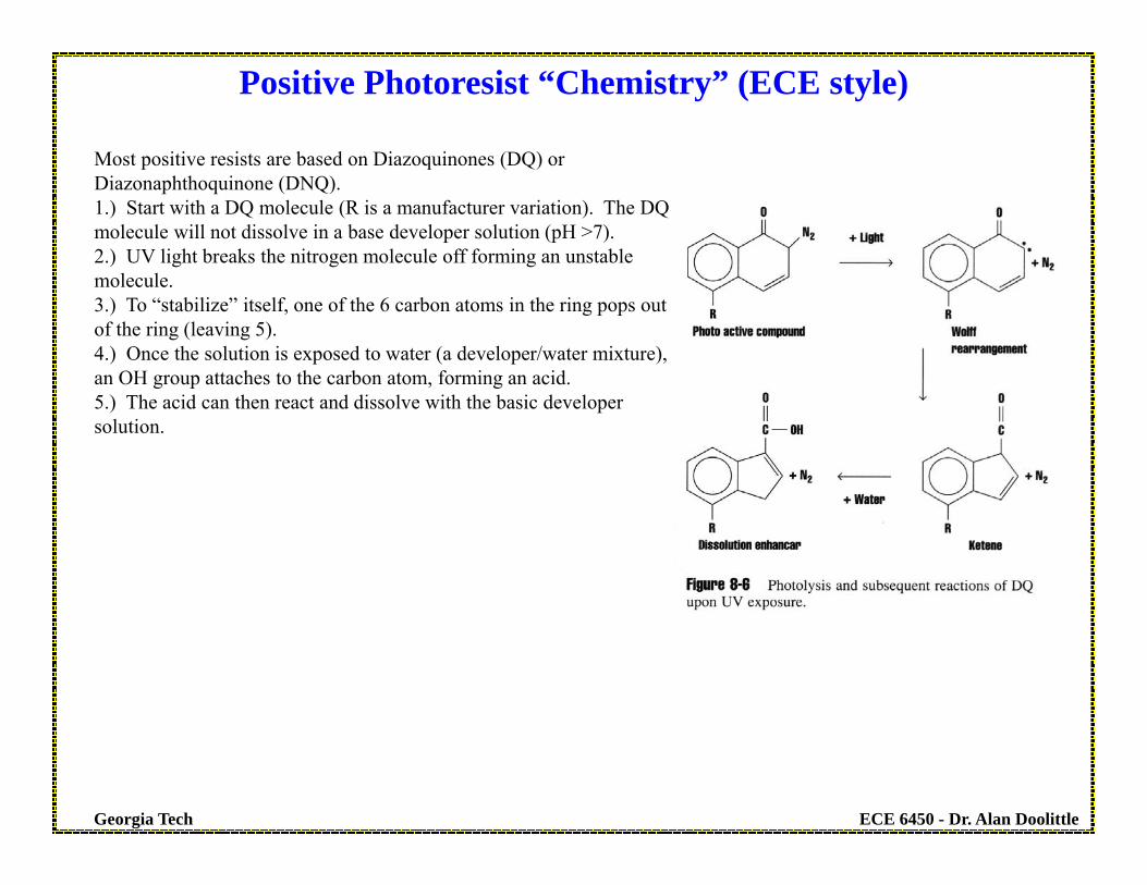
Most positive resists are based on Diazoquinones (DQ) or Diazonaphthoquinone (DNQ). 1.) Start with a DQ molecule (R is a manufacturer variation). The DQ molecule will not dissolve in a base developer solution (pH >7).2.) UV light breaks the nitrogen molecule off forming an unstable molecule.3.) To “stabilize” itself, one of the 6 carbon atoms in the ring pops out of the ring (leaving 5).4.) Once the solution is exposed to water (a developer/water mixture), an OH group attaches to the carbon atom, forming an acid.5.) The acid can then react and dissolve with the basic developer solution.
Positive Photoresist “Chemistry” (ECE style)
ECE 6450 - Dr. Alan DoolittleGeorgia Tech
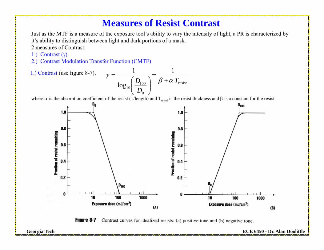
1.) Contrast (use figure 8-7),
resistTD
D
1
log
1
0
10010
Just as the MTF is a measure of the exposure tool’s ability to vary the intensity of light, a PR is characterized by it’s ability to distinguish between light and dark portions of a mask.2 measures of Contrast:1.) Contrast ()2.) Contrast Modulation Transfer Function (CMTF)
Measures of Resist Contrast
where is the absorption coefficient of the resist (1/length) and Tresist is the resist thickness and is a constant for the resist.
ECE 6450 - Dr. Alan DoolittleGeorgia Tech
110110
/1
/1
0100
0100
DDDDCTMFresist
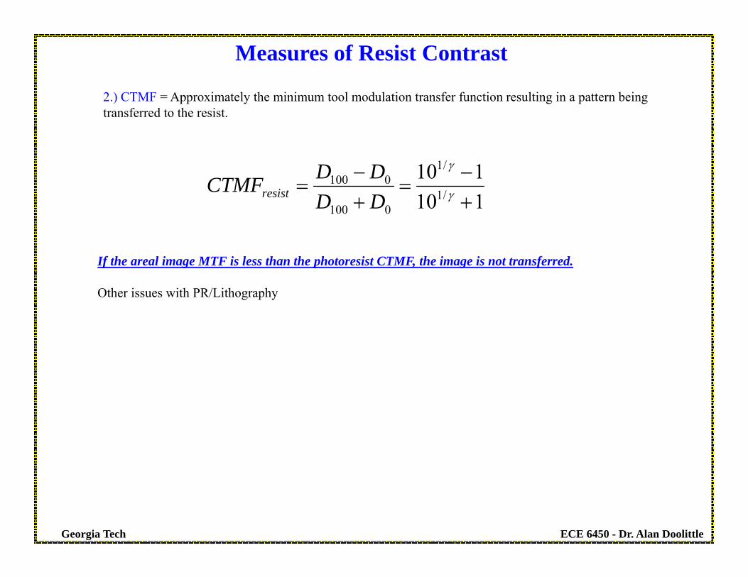
2.) CTMF = Approximately the minimum tool modulation transfer function resulting in a pattern being transferred to the resist.
If the areal image MTF is less than the photoresist CTMF, the image is not transferred.
Other issues with PR/Lithography
Measures of Resist Contrast
ECE 6450 - Dr. Alan DoolittleGeorgia Tech
zzoeIzI )(
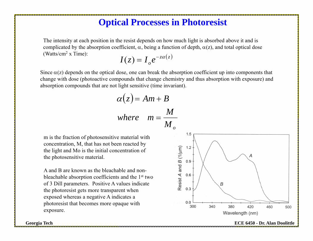
The intensity at each position in the resist depends on how much light is absorbed above it and is complicated by the absorption coefficient, , being a function of depth, (z), and total optical dose (Watts/cm2 x Time):
Optical Processes in Photoresist
Since (z) depends on the optical dose, one can break the absorption coefficient up into components that change with dose (photoactive compounds that change chemistry and thus absorption with exposure) and absorption compounds that are not light sensitive (time invariant).
oMMmwhere
BAmz
m is the fraction of photosensitive material with concentration, M, that has not been reacted by the light and Mo is the initial concentration of the photosensitive material.
A and B are known as the bleachable and non-bleachable absorption coefficients and the 1st two of 3 Dill parameters. Positive A values indicate the photoresist gets more transparent when exposed whereas a negative A indicates a photoresist that becomes more opaque with exposure.
ECE 6450 - Dr. Alan DoolittleGeorgia Tech
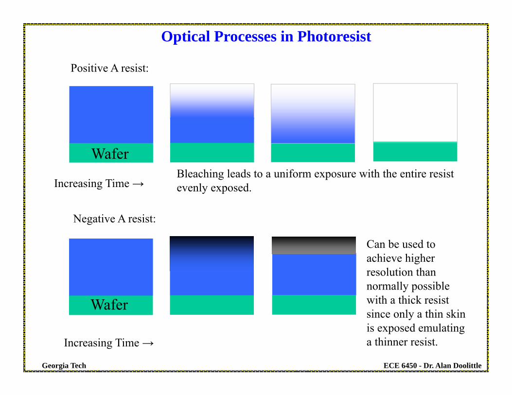
Positive A resist:
Optical Processes in Photoresist
Negative A resist:
Increasing Time →
Can be used to achieve higher resolution than normally possible with a thick resist since only a thin skin is exposed emulating a thinner resist.Increasing Time →
Bleaching leads to a uniform exposure with the entire resist evenly exposed.
Wafer
Wafer
ECE 6450 - Dr. Alan DoolittleGeorgia Tech
)()(
)()()(
zItCezm
zIzCmdt
zdm
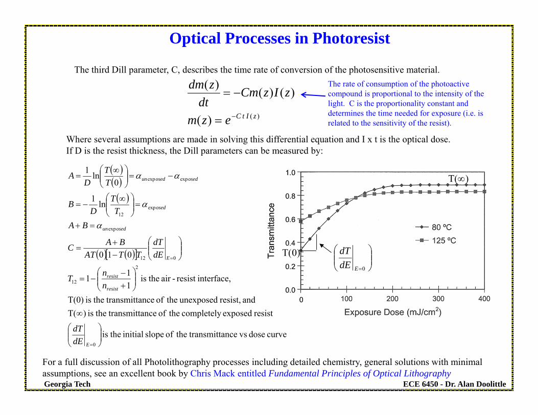
The third Dill parameter, C, describes the time rate of conversion of the photosensitive material.
Optical Processes in Photoresist
Where several assumptions are made in solving this differential equation and I x t is the optical dose.If D is the resist thickness, the Dill parameters can be measured by:
For a full discussion of all Photolithography processes including detailed chemistry, general solutions with minimal assumptions, see an excellent book by Chris Mack entitled Fundamental Principles of Optical Lithography
curve dose vsance transmitt theof slope initial theis
resist exposed completely theof ance transmitt theis )T( and resist, unexposed theof ance transmitt theis T(0)
interface,resist -air theis 111
010
ln1
0ln1
0
2
12
012
exp
exp12
expexp
E
resist
resist
E
osedun
osed
osedosedun
dEdT
nnT
dEdT
TTATBAC
BAT
TD
B
TT
DA
0EdEdT
)T(
)0T(
The rate of consumption of the photoactive compound is proportional to the intensity of the light. C is the proportionality constant and determines the time needed for exposure (i.e. is related to the sensitivity of the resist).
ECE 6450 - Dr. Alan DoolittleGeorgia Tech
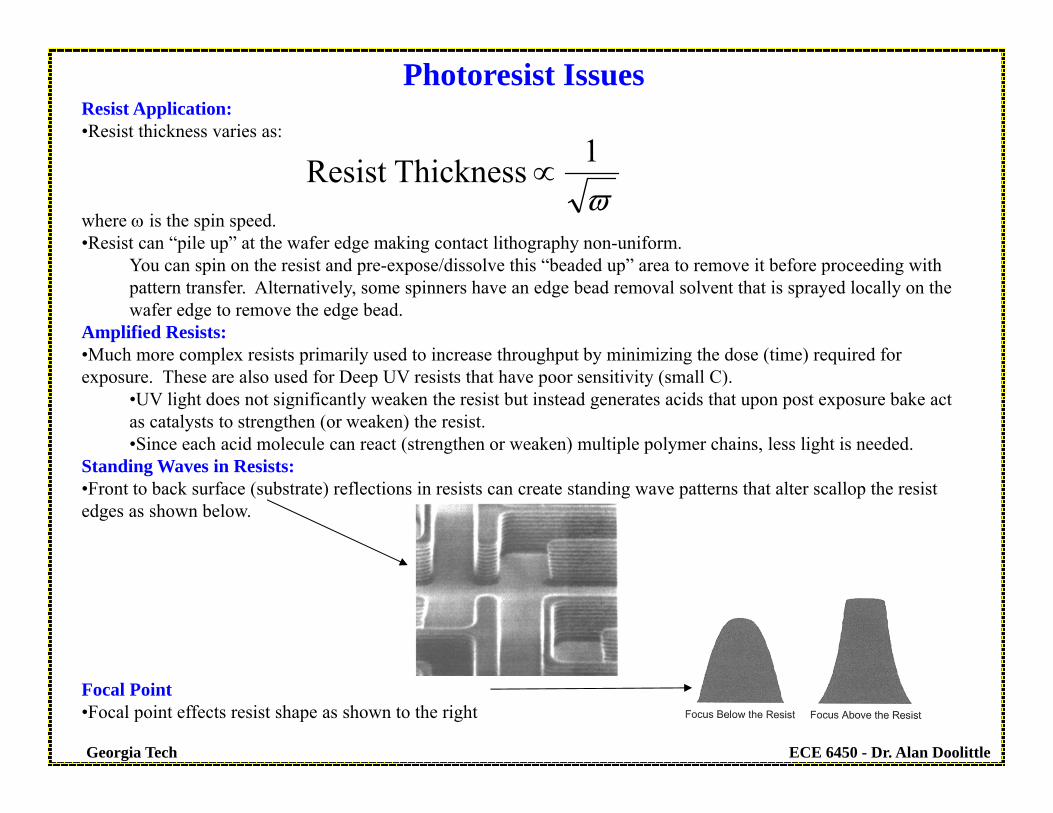
Resist Application:•Resist thickness varies as:
where is the spin speed.•Resist can “pile up” at the wafer edge making contact lithography non-uniform.
You can spin on the resist and pre-expose/dissolve this “beaded up” area to remove it before proceeding with pattern transfer. Alternatively, some spinners have an edge bead removal solvent that is sprayed locally on the wafer edge to remove the edge bead.
Amplified Resists:•Much more complex resists primarily used to increase throughput by minimizing the dose (time) required for exposure. These are also used for Deep UV resists that have poor sensitivity (small C).
•UV light does not significantly weaken the resist but instead generates acids that upon post exposure bake act as catalysts to strengthen (or weaken) the resist.•Since each acid molecule can react (strengthen or weaken) multiple polymer chains, less light is needed.
Standing Waves in Resists:•Front to back surface (substrate) reflections in resists can create standing wave patterns that alter scallop the resist edges as shown below.
Focal Point•Focal point effects resist shape as shown to the right
1ThicknessResist
Photoresist Issues
ECE 6450 - Dr. Alan DoolittleGeorgia Tech
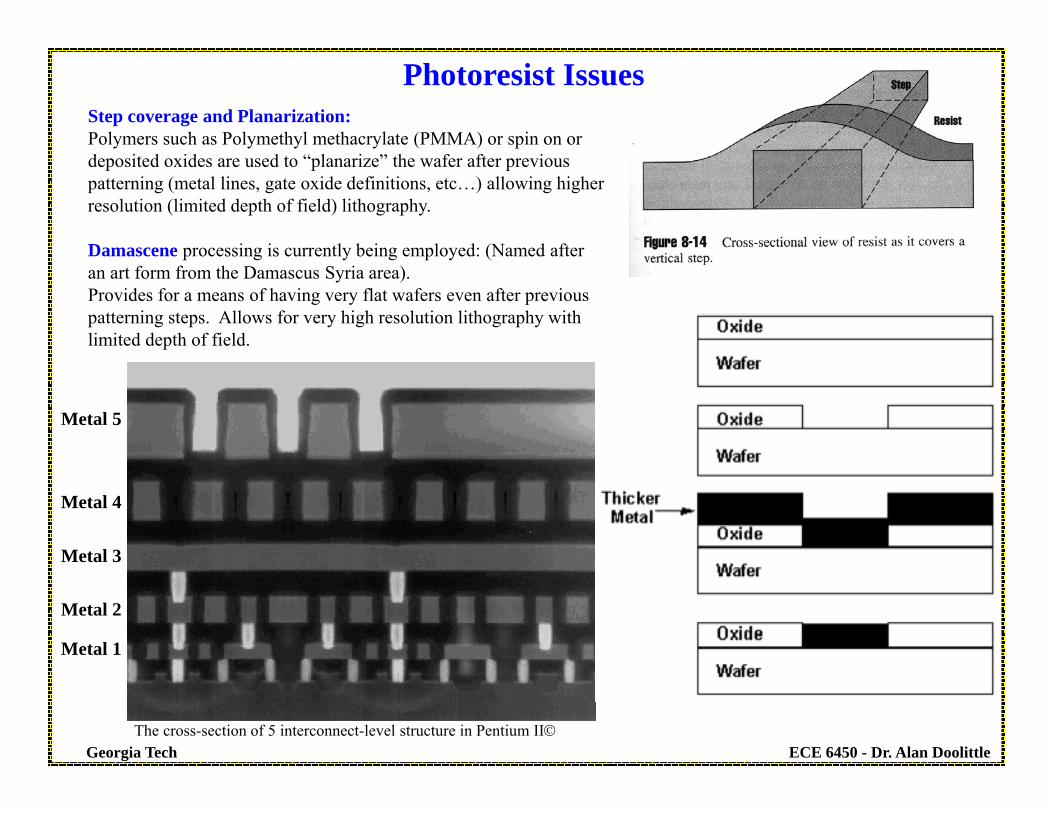
Step coverage and Planarization:Polymers such as Polymethyl methacrylate (PMMA) or spin on or deposited oxides are used to “planarize” the wafer after previous patterning (metal lines, gate oxide definitions, etc…) allowing higher resolution (limited depth of field) lithography.
Damascene processing is currently being employed: (Named after an art form from the Damascus Syria area).Provides for a means of having very flat wafers even after previous patterning steps. Allows for very high resolution lithography with limited depth of field.
The cross-section of 5 interconnect-level structure in Pentium II
Photoresist Issues
Metal 1
Metal 2
Metal 3
Metal 4
Metal 5
ECE 6450 - Dr. Alan DoolittleGeorgia Tech
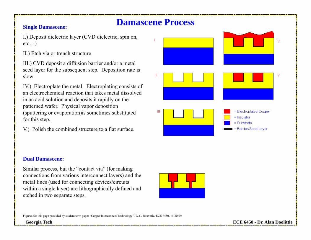
Damascene Process
Figures for this page provided by student term paper “Copper Interconnect Technology”, W.C. Bouverie, ECE 6450, 11/30/99
Single Damascene:
I.) Deposit dielectric layer (CVD dielectric, spin on, etc…)
II.) Etch via or trench structure
III.) CVD deposit a diffusion barrier and/or a metal seed layer for the subsequent step. Deposition rate is slow
IV.) Electroplate the metal. Electroplating consists of an electrochemical reaction that takes metal dissolved in an acid solution and deposits it rapidly on the patterned wafer. Physical vapor deposition (sputtering or evaporation)is sometimes substituted for this step.
V.) Polish the combined structure to a flat surface.
Dual Damascene:
Similar process, but the “contact via” (for making connections from various interconnect layers) and the metal lines (used for connecting devices/circuits within a single layer) are lithographically defined and etched in two separate steps.
ECE 6450 - Dr. Alan DoolittleGeorgia Tech
Advanced Lithography
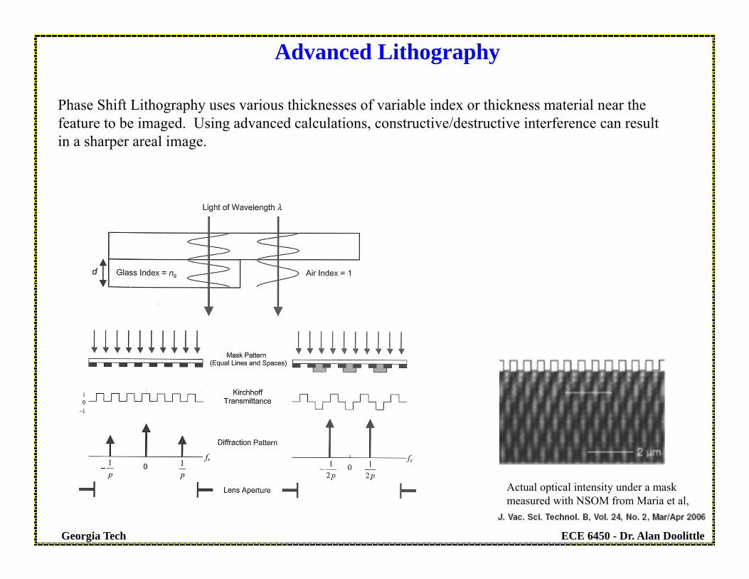
Phase Shift Lithography uses various thicknesses of variable index or thickness material near the feature to be imaged. Using advanced calculations, constructive/destructive interference can result in a sharper areal image.
Actual optical intensity under a mask measured with NSOM from Maria et al,
ECE 6450 - Dr. Alan DoolittleGeorgia Tech
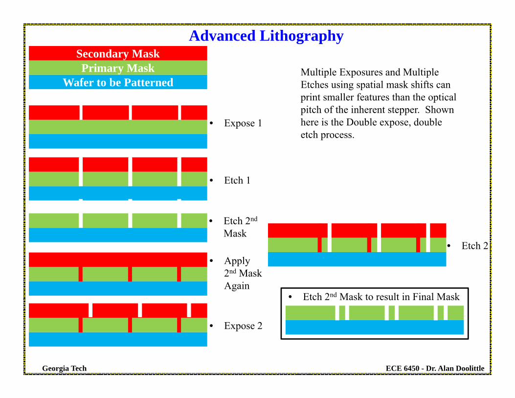
Advanced Lithography
Multiple Exposures and Multiple Etches using spatial mask shifts can print smaller features than the optical pitch of the inherent stepper. Shown here is the Double expose, double etch process.
Wafer to be PatternedPrimary Mask
Secondary Mask
• Expose 1
• Etch 1
• Expose 2
• Etch 2
• Etch 2nd Mask to result in Final Mask
• Apply 2nd Mask Again
• Etch 2nd
Mask
ECE 6450 - Dr. Alan DoolittleGeorgia Tech
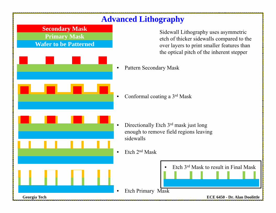
Advanced LithographySidewall Lithography uses asymmetric etch of thicker sidewalls compared to the over layers to print smaller features than the optical pitch of the inherent stepper
Wafer to be PatternedPrimary Mask
Secondary Mask
• Pattern Secondary Mask
• Conformal coating a 3rd Mask
• Directionally Etch 3rd mask just long enough to remove field regions leaving sidewalls
• Etch 2nd Mask
• Etch Primary Mask
• Etch 3rd Mask to result in Final Mask
ECE 6450 - Dr. Alan DoolittleGeorgia Tech
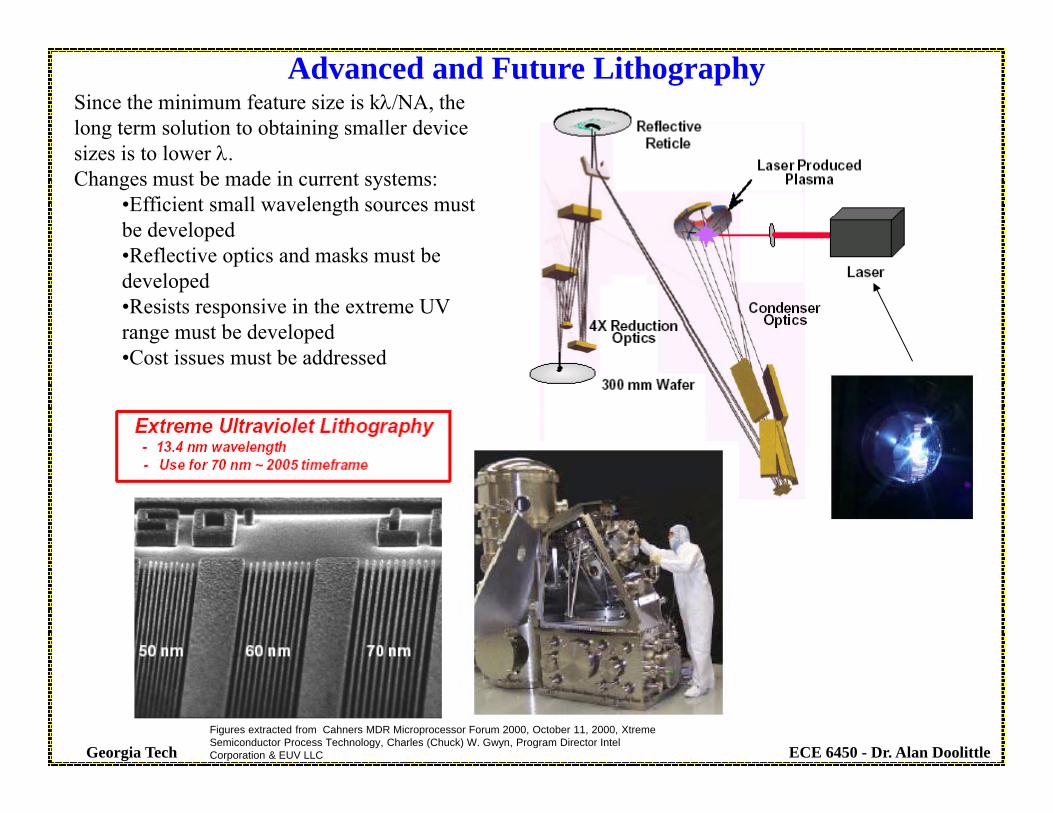
Advanced and Future Lithography
Figures extracted from Cahners MDR Microprocessor Forum 2000, October 11, 2000, Xtreme Semiconductor Process Technology, Charles (Chuck) W. Gwyn, Program Director Intel Corporation & EUV LLC
Since the minimum feature size is k/NA, the long term solution to obtaining smaller device sizes is to lower .Changes must be made in current systems:
•Efficient small wavelength sources must be developed•Reflective optics and masks must be developed•Resists responsive in the extreme UV range must be developed•Cost issues must be addressed
ECE 6450 - Dr. Alan DoolittleGeorgia Tech
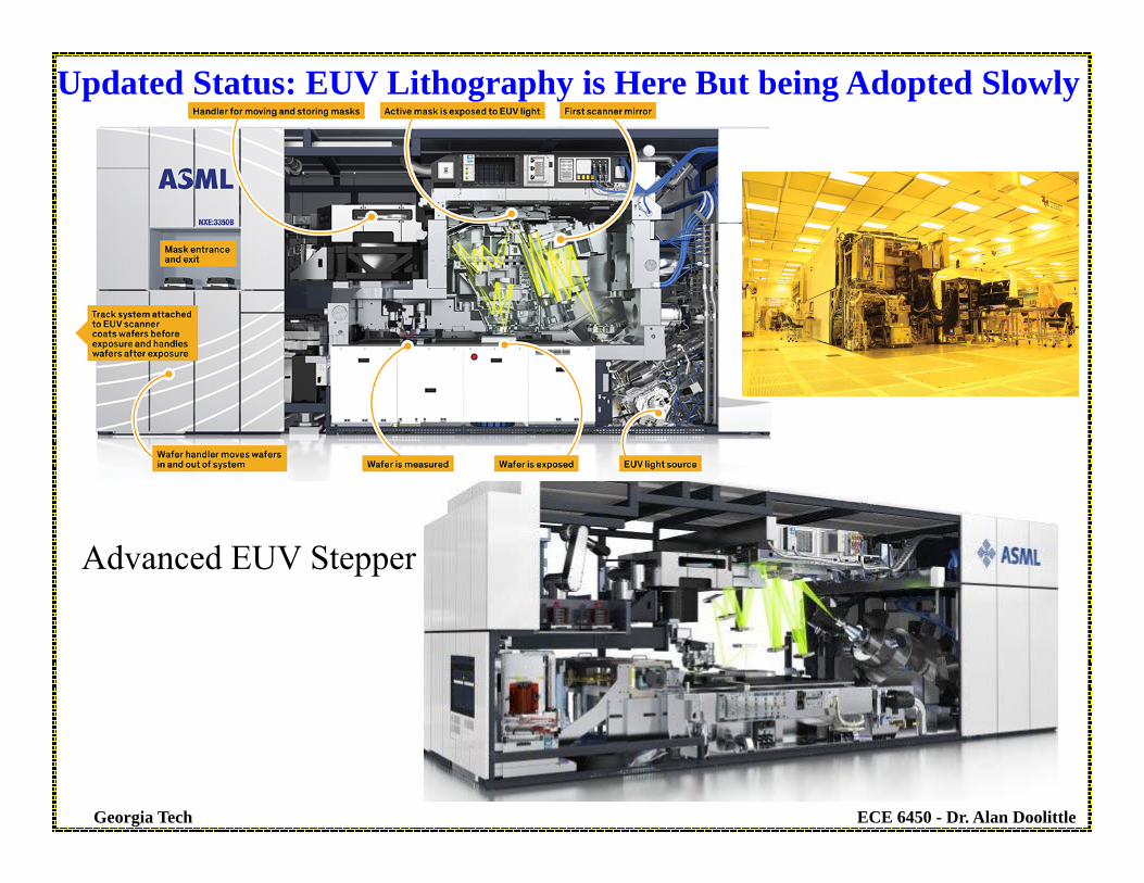
Advanced EUV Stepper
Updated Status: EUV Lithography is Here But being Adopted Slowly
ECE 6450 - Dr. Alan DoolittleGeorgia Tech
Advanced and Future Lithography
Other companies/universities are taking the approach of using X-Rays or Electrons for low volume lithography:
X-Rays:Advantages:
•Very small wavelength (1.5 Angstroms or shorter)•Can be performed in air, but particles are a problem
Disadvantages:•Bright sources of X-rays exist, but are still not bright enough for high throughput.•Polished mirrors are very difficult and expensive to make and maintain.•Shares all of EUVL problems.
Electron Beam Lithography:Advantages:
•Extremely small wavelength (<0.01 Angstroms or shorter)•Viable solutions for 10 nm features are available TODAY.•No mirrors required.•Limited need for optics.
Disadvantages:•Bright sources of do not exist resulting in very limited throughput.•Vacuum based technology.