Embed Size (px)
Citation preview
1
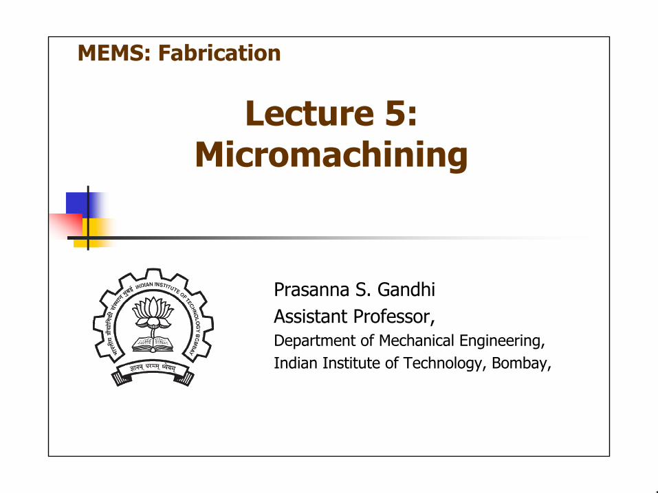
Lecture 5: Micromachining
Prasanna S. GandhiAssistant Professor,Department of Mechanical Engineering,Indian Institute of Technology, Bombay,
MEMS: Fabrication
2
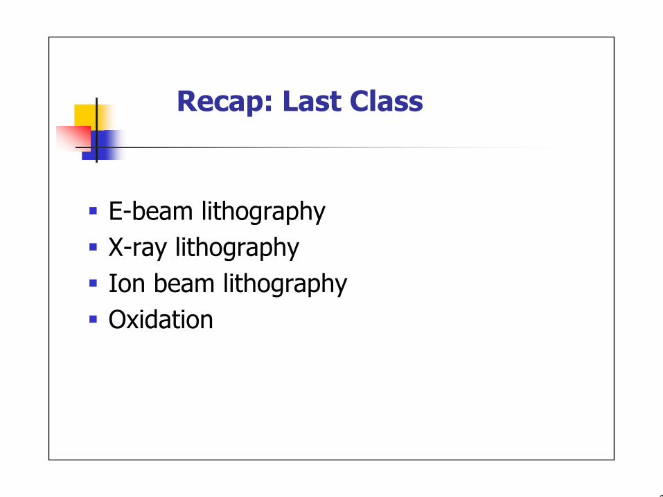
Recap: Last Class
E-beam lithographyX-ray lithographyIon beam lithographyOxidation
3
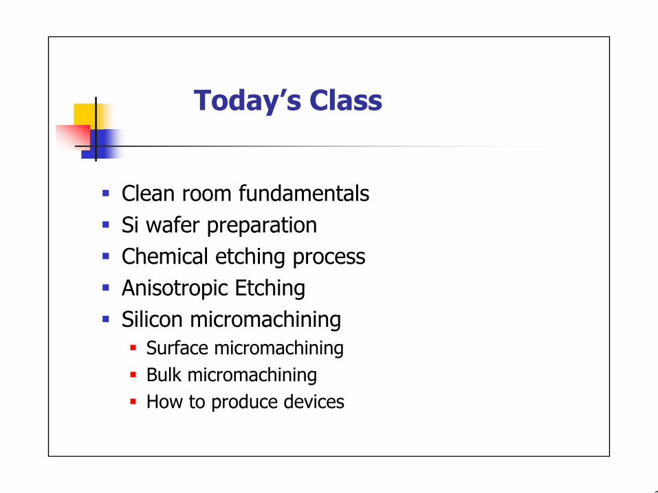
Today’s Class
Clean room fundamentals Si wafer preparationChemical etching processAnisotropic EtchingSilicon micromachining
Surface micromachiningBulk micromachiningHow to produce devices
4
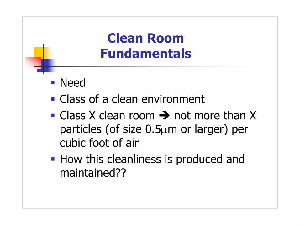
Clean Room Fundamentals
NeedClass of a clean environmentClass X clean room not more than X particles (of size 0.5µm or larger) per cubic foot of airHow this cleanliness is produced and maintained??
5
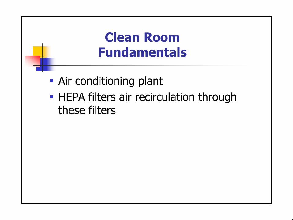
Clean Room Fundamentals
Air conditioning plantHEPA filters air recirculation through these filters
6
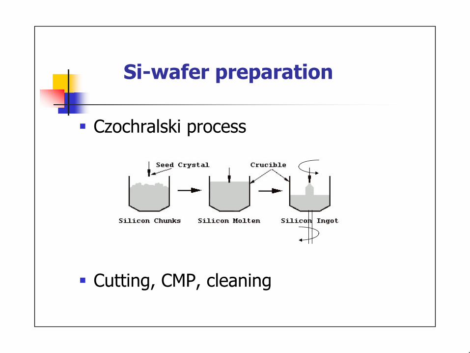
Si-wafer preparation
Czochralski process
Cutting, CMP, cleaning
7
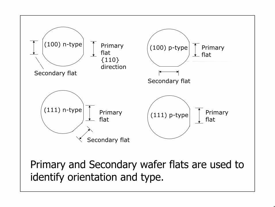
Secondary flat
Primary flat
Secondary flat
Primary flat {110} direction
Primary flat
Primary flat
Secondary flat
Primary and Secondary wafer flats are used to identify orientation and type.
(100) n-type (100) p-type
(111) n-type(111) p-type
8
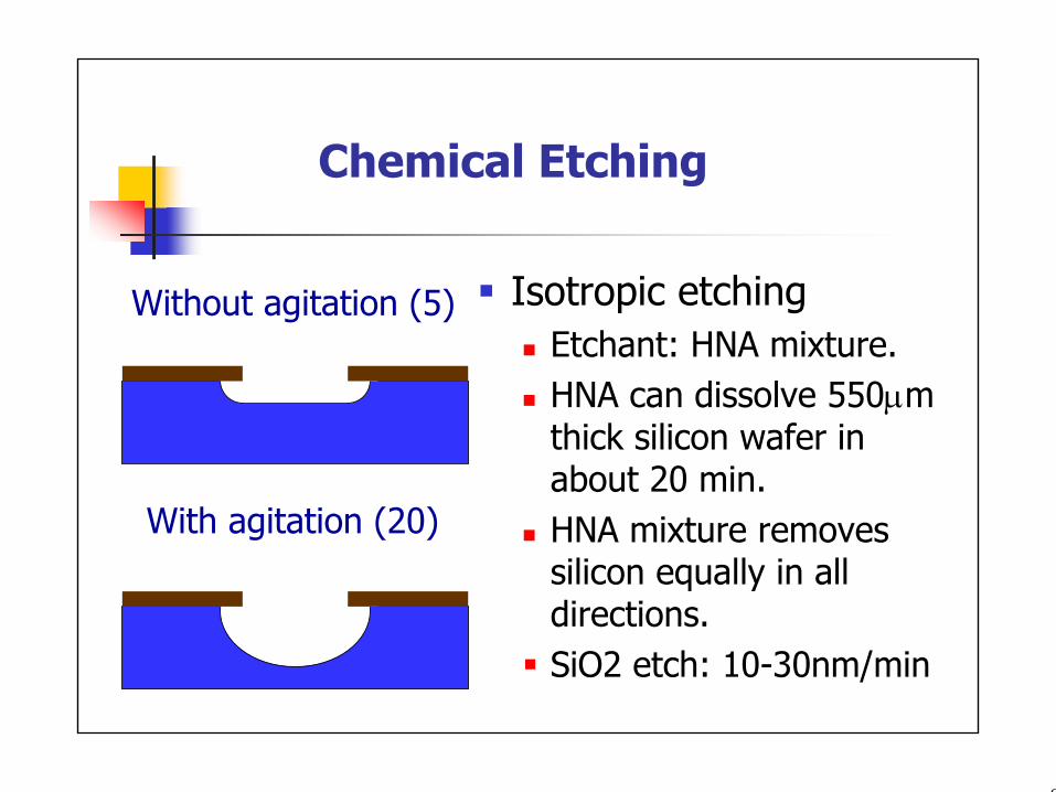
Chemical Etching
Isotropic etchingEtchant: HNA mixture.HNA can dissolve 550µm thick silicon wafer in about 20 min.HNA mixture removes silicon equally in all directions.SiO2 etch: 10-30nm/min
Without agitation (5)
With agitation (20)
9
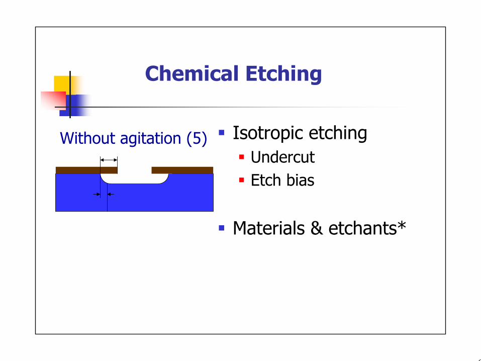
Chemical Etching
Isotropic etchingUndercutEtch bias
Materials & etchants*
Without agitation (5)
10
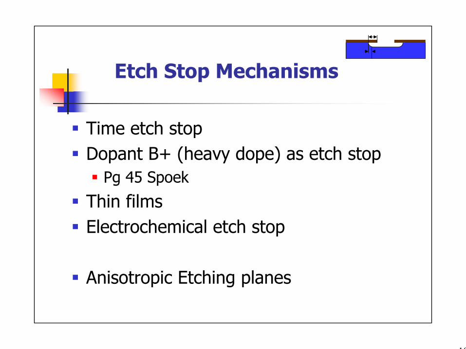
Etch Stop Mechanisms
Time etch stopDopant B+ (heavy dope) as etch stop
Pg 45 Spoek
Thin filmsElectrochemical etch stop
Anisotropic Etching planes
11
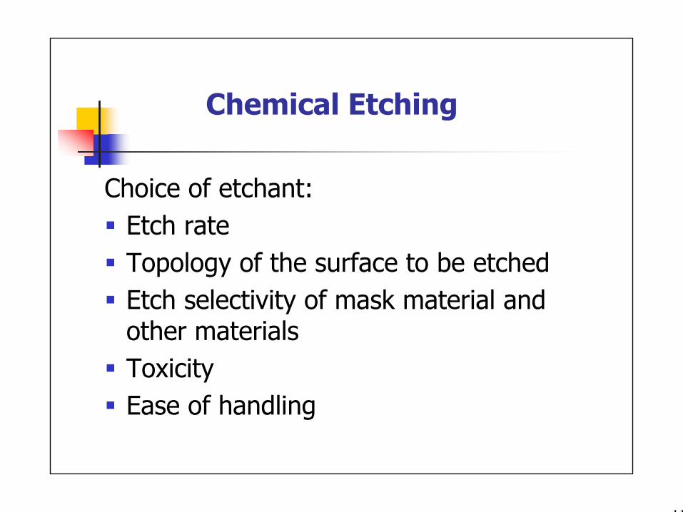
Chemical Etching
Choice of etchant:Etch rateTopology of the surface to be etchedEtch selectivity of mask material and other materials ToxicityEase of handling
12
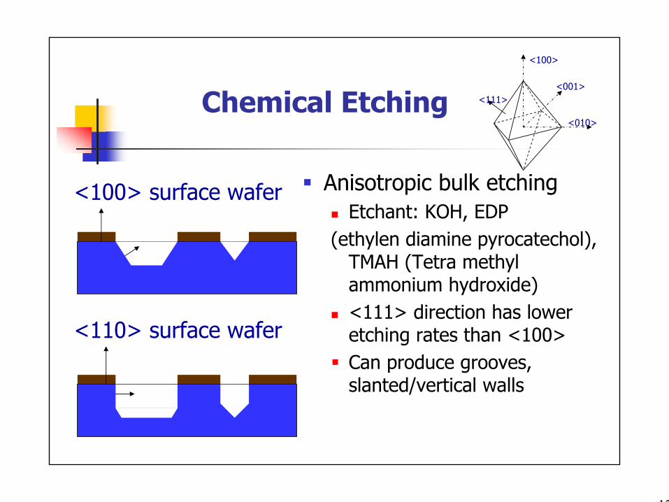
Chemical Etching
Anisotropic bulk etchingEtchant: KOH, EDP
(ethylen diamine pyrocatechol), TMAH (Tetra methyl ammonium hydroxide)<111> direction has lower etching rates than <100>Can produce grooves, slanted/vertical walls
<110> surface wafer
<100>
<010>
<001><111>
<100> surface wafer
13
Chemical Etching
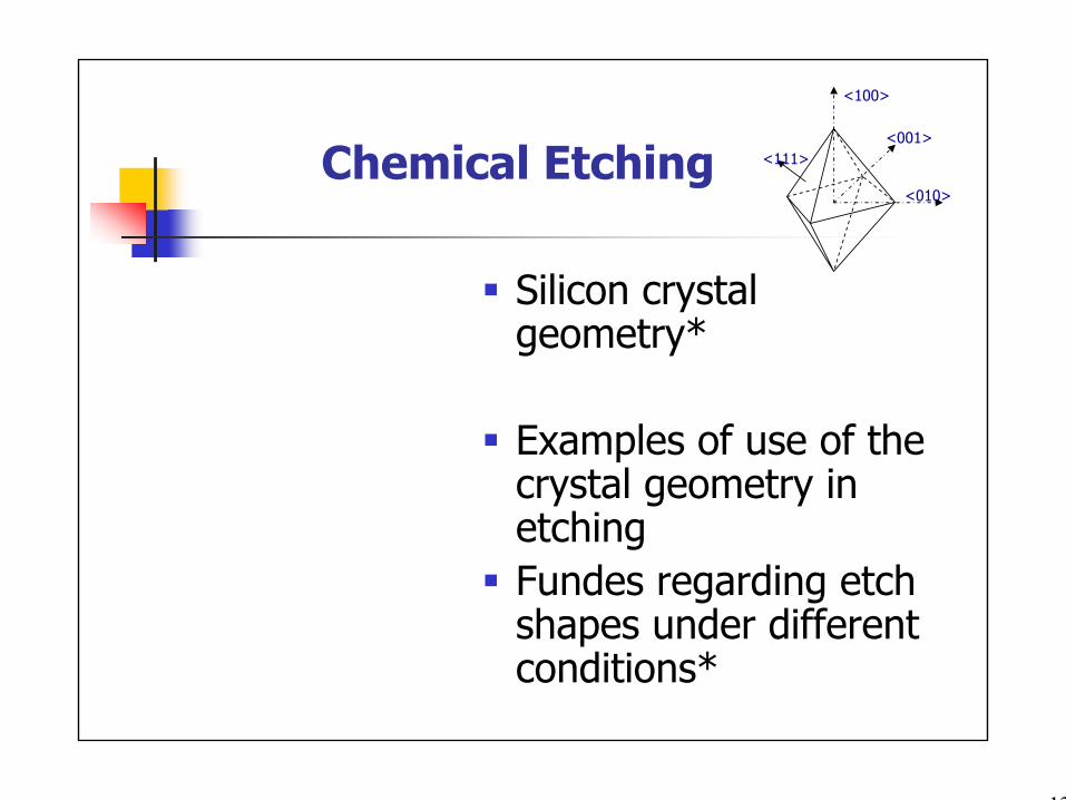
Silicon crystal geometry*
Examples of use of the crystal geometry in etchingFundes regarding etch shapes under different conditions*
<100>
<010>
<001><111>

14
Anisotropic Etching
KOH, EDP and TMAHEDP etches oxide 100 times slower than KOH, KOH, TMAH dangerous to eyeKOH less dangerous than EDP & TMAHEtch curves*: 5hrs to etch 300µm thick waferH2 bubbles during KOH etching of SiEDP ages quickly in contact with oxygen producing red brown color, vapor is harmfulHF dip is necessary for EDP: native oxide problem
<100>
<010>
<001><111>
15
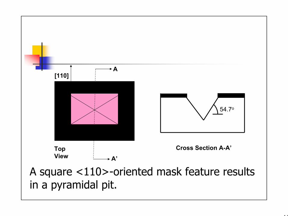
A’
A
Top View
[110]
54.7o
Cross Section A-A’
A square <110>-oriented mask feature results in a pyramidal pit.

16
A
A’A
A’A
A’
Convex corners are rapidly undercut
54.7o
[100] Silicon
[110][100] Masking Layer
Cross Section A-A’
[100]
Cross Section A-A’
Convex corners where {111} planes meet are not stable. They are rapidly undercut. This permits creation of suspended structures.
17
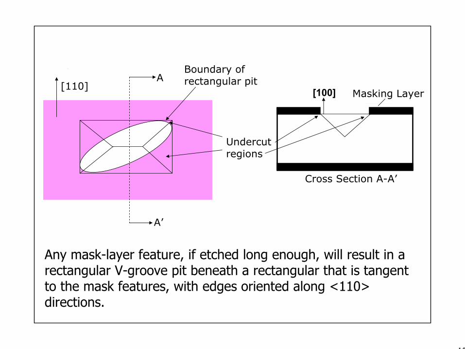
A’
ABoundary of rectangular pit[110]
Undercut regions
[100] Masking Layer
Cross Section A-A’
Any mask-layer feature, if etched long enough, will result in a rectangular V-groove pit beneath a rectangular that is tangent to the mask features, with edges oriented along <110> directions.
18
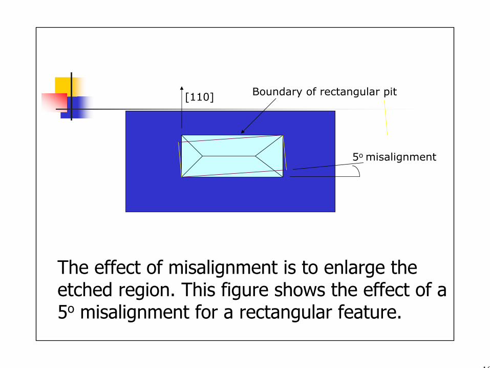
The effect of misalignment is to enlarge the etched region. This figure shows the effect of a 5o misalignment for a rectangular feature.
5o misalignment
Boundary of rectangular pit[110]
19
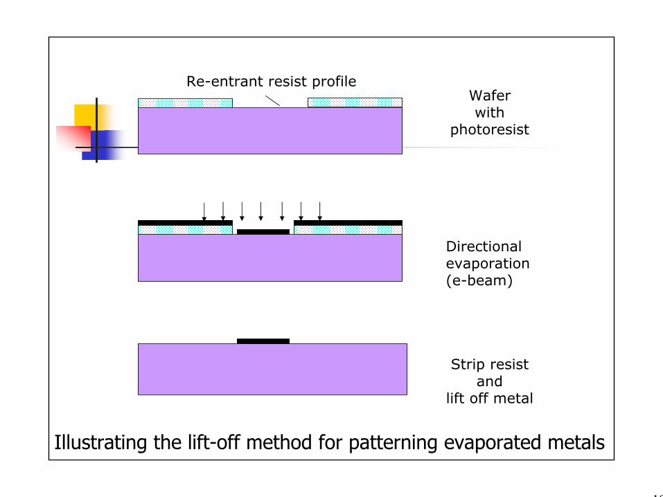
Re-entrant resist profileWafer with
photoresist
Directional evaporation (e-beam)
Strip resist and
lift off metal
Illustrating the lift-off method for patterning evaporated metals
20
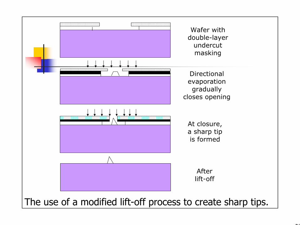
Wafer with double-layer
undercut masking
Directional evaporation gradually
closes opening
At closure, a sharp tip is formed
The use of a modified lift-off process to create sharp tips.
After lift-off
21
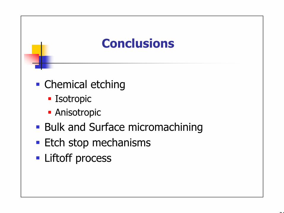
Conclusions
Chemical etchingIsotropic Anisotropic
Bulk and Surface micromachiningEtch stop mechanismsLiftoff process

22
Next class
Plasma based processesPlasma etchingRIE
SputteringPE CVD

23
Wafer Cleaning Process
NeedCMP- Chemical mechanical polishing
RCA cleaning
24
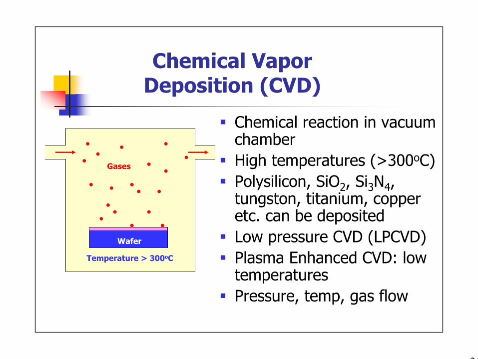
Chemical Vapor Deposition (CVD)
Chemical reaction in vacuum chamberHigh temperatures (>300oC)Polysilicon, SiO2, Si3N4, tungston, titanium, copper etc. can be depositedLow pressure CVD (LPCVD)Plasma Enhanced CVD: low temperaturesPressure, temp, gas flow
Wafer
Gases
Temperature > 300oC
25
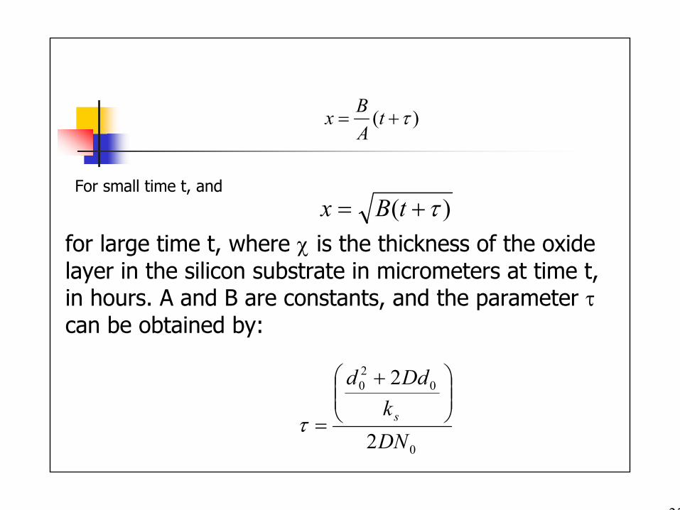
)( τ+= tBx
)( τ+= tABx
For small time t, and
0
020
2
2
DNkDdd
s
+
=τ
for large time t, where χ is the thickness of the oxide layer in the silicon substrate in micrometers at time t, in hours. A and B are constants, and the parameter τcan be obtained by:
26
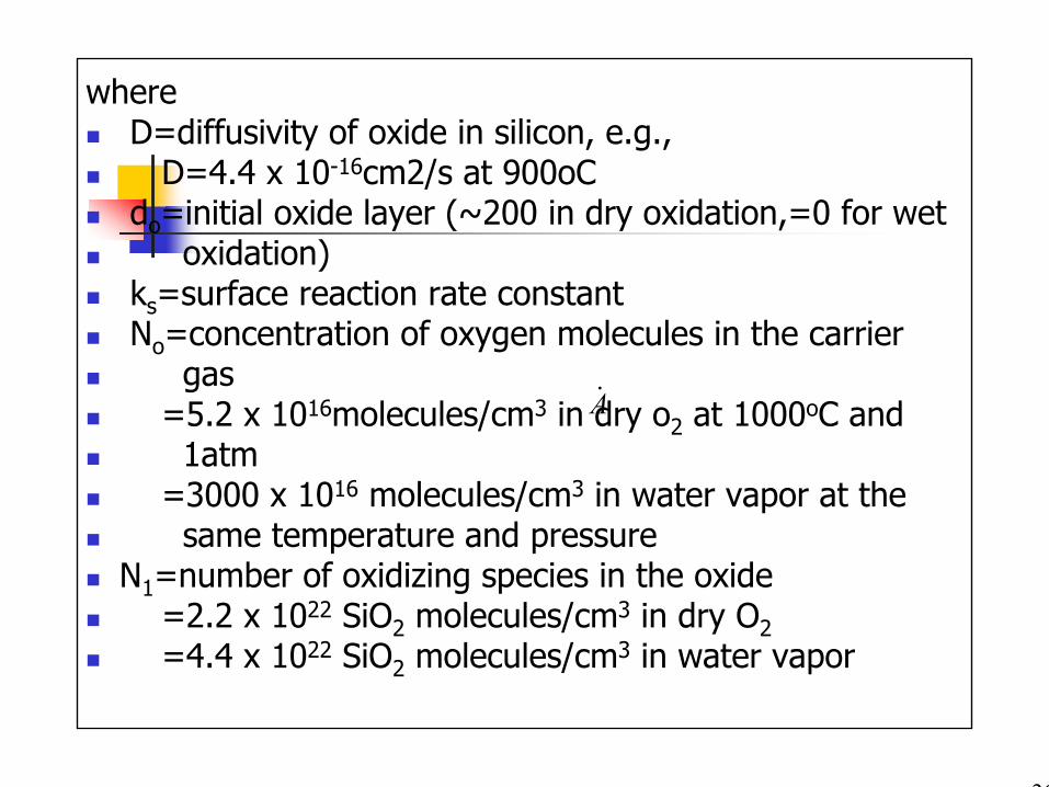
whereD=diffusivity of oxide in silicon, e.g.,
D=4.4 x 10⁻¹⁶cm2/s at 900oCdo=initial oxide layer (~200 in dry oxidation,=0 for wet
oxidation)ks=surface reaction rate constantNo=concentration of oxygen molecules in the carrier
gas=5.2 x 10¹⁶molecules/cm3 in dry o2 at 1000oC and
1atm=3000 x 1016 molecules/cm3 in water vapor at the
same temperature and pressureN1=number of oxidizing species in the oxide
=2.2 x 10²² SiO2 molecules/cm3 in dry O2=4.4 x 10²² SiO2 molecules/cm3 in water vapor
A