Embed Size (px)
Citation preview

Mixed-Signal Design and Automation Methods
混合信号电路设计与自动化方法
Lecture 2 Preliminary for Analog IC Design
Prof. Guoyong Shi [email protected]
Department of Micro/Nano-electronics Shanghai Jiao Tong University
Fall 2015

Lecture 2 slide 2 2015
Outline • Reference books on opamp circuit design • Building block cells for analog IC • Transistor model and basic design equations • Circuit simulation (recommended simulators)
Lecture 2 slide 3 2015
Textbooks (Recommended)
1. D.A. Johns and K. Martin, Analog Integrated Circuit Design, NY, Wiley, 1997.
2. B. Razavi, Design of Analog CMOS Integrated Circuits, McGraw Hill, 2001.
3. P.E. Allen and D.R. Holberg, CMOS Analog Circuit Design, 2nd Ed., NY, Oxford university Press, 2002.
You may find the basic amplifier design information in these popular textbooks.
Lecture 2 slide 4 2015
More Advanced Research Books
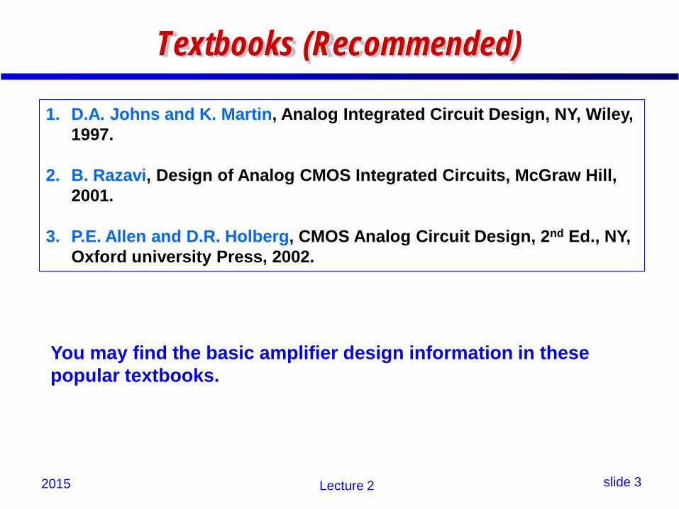
1. R. Hogervorst, and J.H. Huijsing, Design of Low-voltage, Low-power Operational Amplifier Cells, Kluwer, 1996.
2. K.-J. de Langen, and J.H. Huijsing, Compact Low-voltage and High-speed CMOS, BiCMOS and Bipolar Operational Amplifiers, Kluwer, 1999.
3. J. H. Huijsing, Operational Amplifiers, Kluwer, Boston, 2001. 4. V. V. Ivanov, I. M. Filanovsky, Operational Amplifier Speed and Accuracy
Improvement, Kluwer, Boston, 2004 (folded cascode and current mirror improvements using current amplifiers)
For more advanced materials, you may refer to the following books.

Lecture 2 slide 5 2015
A Basic Opamp
• Differential PMOS input, single output • Miller compensation

Lecture 2 slide 6 2015
Circuit Basics • A basic opamp includes
– Biasing circuit – Input stage (differential PMOS transistor stage with
differential to single ended conversion, and output stage. – Compensation capacitor Cc, and
• The basic parameters of this amplifier:
• DC gain • Bandwidth • Slew-rate (SR) • Offset and noise referred to the input.

Lecture 2 slide 7 2015
Opamps • Loosely an opamp is a “high-gain operational
amplifier”. • By “high”, we mean a value anywhere between 10 to
105 (100dB). • Opamps are usually used in a feedback system,
when an operation must be performed precisely.
Lecture 2 slide 8 2015
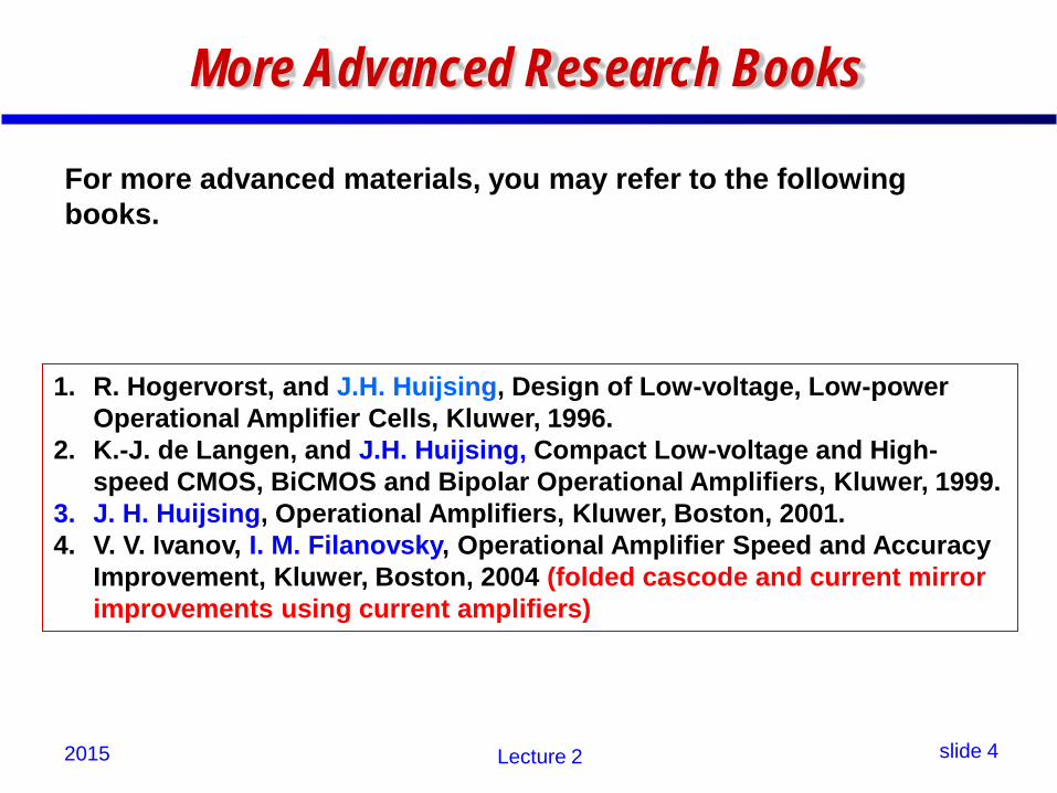
Ideal Opamp • AV = inf, Rin = inf, Rout = 0 • without considering: power, output swing, and
speed. • Modern opamps are designed for a specific
application, – often trading unimportant aspects for the important ones.
• e.g., most of today’s CMOS opamps have a high output impedance (in open loop) – for supplying a current to the load
• they are often called “transconductance amplifiers” – i.e. voltage-to-current amplifier (like the effect of gm)

Lecture 2 slide 9 2015
Typical Performance Metrics • Gain, speed, output swing, linearity, power
dissipation; • Noise, input CM range, supply rejection; • Input offset voltage VOS ; • etc.
• All these metrics are related to the transistor-level
details.

Lecture 2 slide 10 2015
Building Blocks (Cells)

Lecture 2 slide 11 2015
Cell-based Design • Just like the design of other electronic circuits, • the design of opamps can be greatly accelerated if
we use a library of simple circuits, sometimes called cells.
• Cell-based design is also a fundamental idea for analog/mixed-signal design automation.

Lecture 2 slide 12 2015
Typical Analog Modules • Operational amplifiers (opamps, V-to-V, V-to-I); • OTA - Operational Transconductance Amplifiers (V-
to-I); • Comparators (in ADC); • Oscillators (in RF frontend); • Voltage references (bandgap) • Temperature compensation • Current references • DC-DC (voltage regulation) • ... • Each requiring special design expertise

Lecture 2 slide 13 2015
Example: Basic Analog Building Blocks
Single transistor (gm)
Simple current mirror
Cascode current mirror
(for higher output impedance)
Load to current mirror
4-transistor current mirror
(for wide swing)
Current mirror bank
(for current-mode design)

Lecture 2 slide 14 2015
Building Blocks (cont’d)
Voltage reference 1
Differential pair
(input)
Level shifter
Voltage reference 2
Flip-Flop
(bistable circuit)
Level shifter bank
T. Massier, H. Graeb, U. Schlichtmann, “The sizing rules method for CMOS and bipolar analog integrated circuit synthesis,” IEEE Trans. on CAD, vol. 27, no. 12, pp. 2209 – 2222, 2008.

Lecture 2 slide 15 2015
Common gate (Gate signal not varying)
Common drain (Drain signal not varying)
Common source (Source signal not varying)
Simple current mirror Cascoded current
mirror
Traditional Cells

Lecture 2 slide 16 2015
Differential pair (differential transconductance amplifier with current as output)
Differential pair with differential input and single-ended output
Traditional Cells (cont’d)

Lecture 2 slide 17 2015
Ambitious Design Goals
Four one-hundreds: By modifying the basic structure, one can achieve the following performance :
•100 dB gain, (= 105) •100 dB CMRR, and •100 dB PSRR.
The obtained amplifier has input and output rail-to-rail operation, and is compensated for 100% feedback operation (operating signal range).
Lecture 2 slide 18 2015
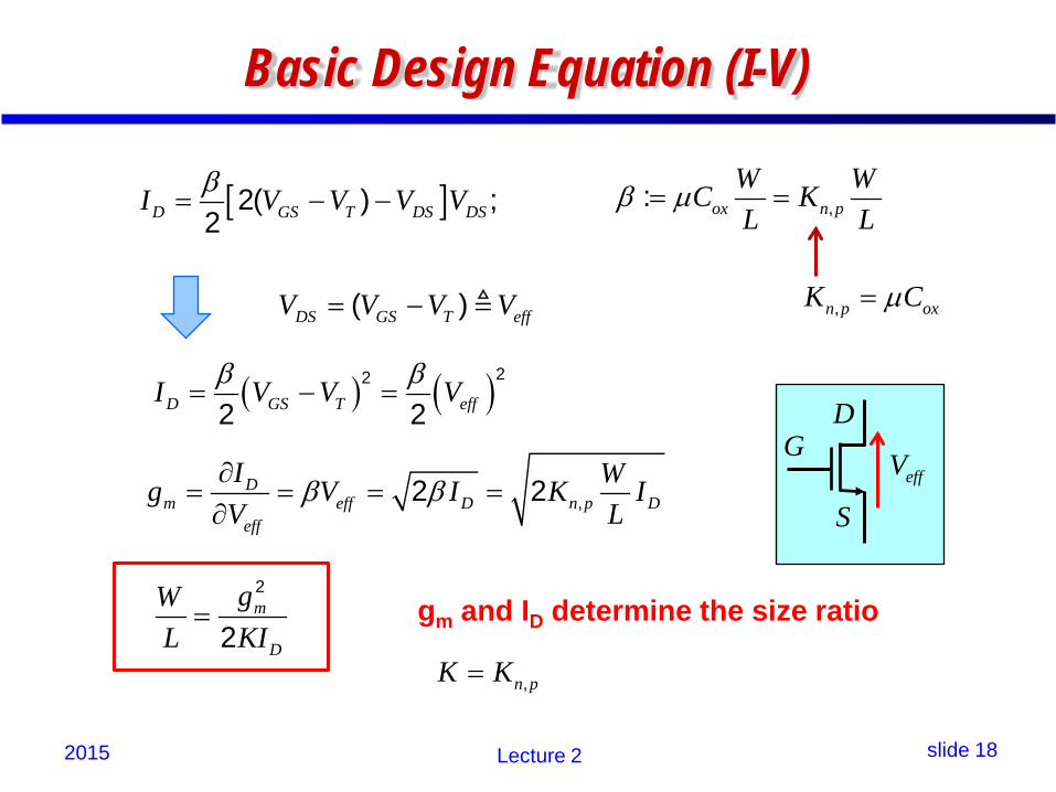
Basic Design Equation (I-V)
[ ]D GS T DS DSI V V V Vβ= − −2( ) ;
2 ,: ox n pW WC KL L
β µ= =
( ) ( )22
2 2D GS T effI V V Vβ β= − =
,2 2Dm eff D n p D
eff
I Wg V I K IV L
β β∂= = = =∂
2
2m
D
gWL KI= gm and ID determine the size ratio
,n p oxK Cµ=( )DS GS T effV V V V= −
,n pK K=
effV
DG
S

Lecture 2 slide 19 2015
MOS Current-Voltage Characteristics
effV 3
When VDS ≥ Veff, ID is in saturation.
That’s why diode connected MOS works in saturation.
DS GS GS T effV V V V V= ≥ − =

Lecture 2 slide 20 2015
Circuit Simulation • I assume all students have experience on HSPICE, at
least on PSPICE.
• HSPICE tutorial
• PSPICE tutorial (www.orcad.org)
• LTspice (www.linear.com) – A simulator by Linear Technology Corp – PC version available (download and install by yourself) – With mixed-signal functionality

Lecture 2 slide 21 2015
Reference • I. M. Filanovsky’s tutorial slides on MWSCAS 2011.