Embed Size (px)
DESCRIPTION
UCSD ECE 230A L1
Citation preview
ECE212AN: Principles of NanoscienceECE212AN: Principles of Nanoscience
Prof. Jie XiangFall 2010
19/24/2010
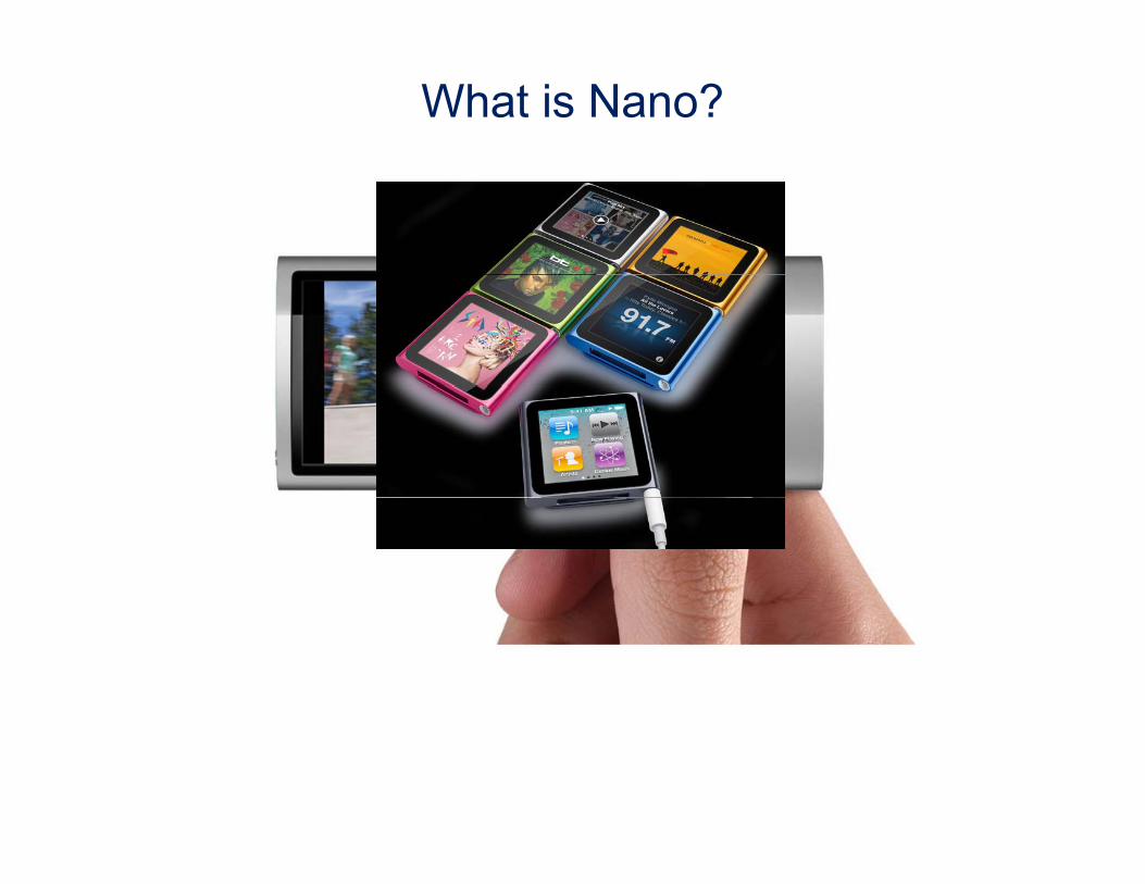
What is Nano?
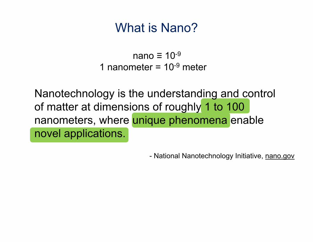
What is Nano?
nano ≡ 10-9
1 nanometer = 10-9 meter
Nanotechnology is the understanding and control of matter at dimensions of roughly 1 to 100of matter at dimensions of roughly 1 to 100 nanometers, where unique phenomena enable novel applications.novel applications.
- National Nanotechnology Initiative, nano.gov
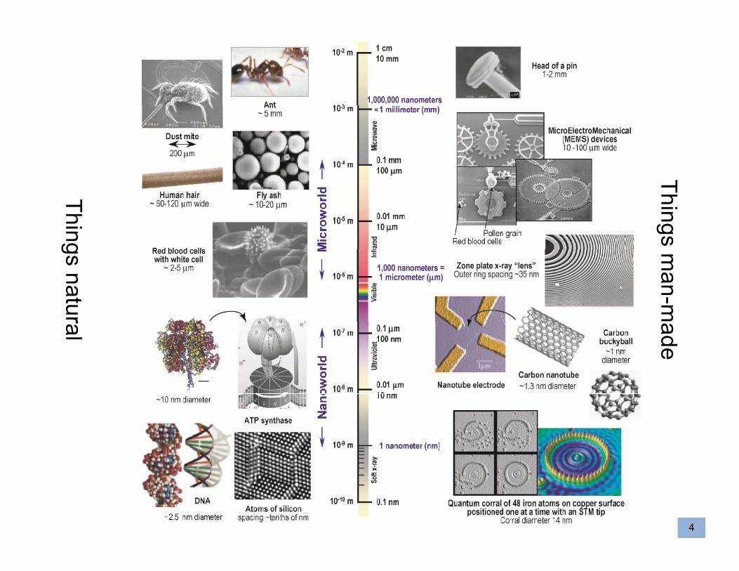
Thing
Things gs natur
man-mral ade
4
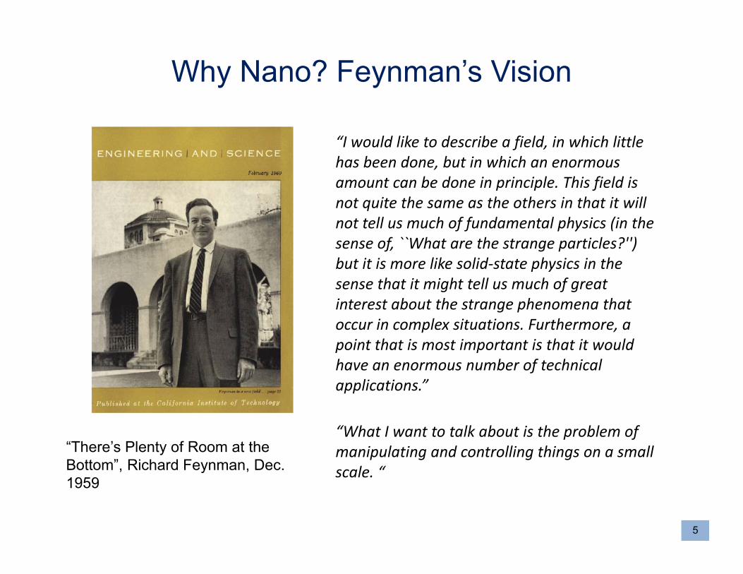
Why Nano? Feynman’s Vision
“I would like to describe a field, in which little has been done, but in which an enormous
t b d i i i l Thi fi ld iamount can be done in principle. This field is not quite the same as the others in that it will not tell us much of fundamental physics (in the sense of, ``What are the strange particles?'') f g p )but it is more like solid‐state physics in the sense that it might tell us much of great interest about the strange phenomena that occur in complex situations Furthermore aoccur in complex situations. Furthermore, a point that is most important is that it would have an enormous number of technical applications.”
“There’s Plenty of Room at the Bottom” Richard Feynman Dec
“What I want to talk about is the problem of manipulating and controlling things on a small
l “
5
Bottom , Richard Feynman, Dec. 1959
scale. “
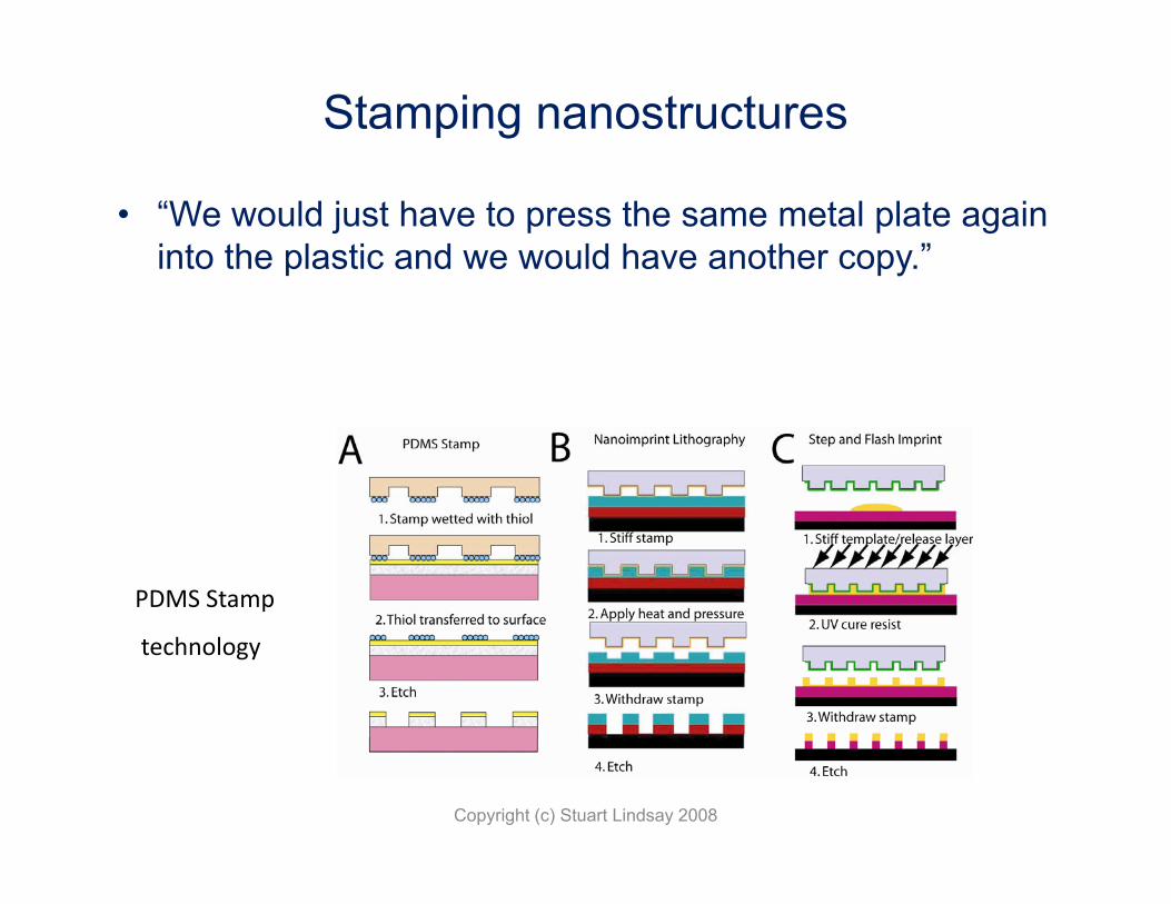
Stamping nanostructures
• “We would just have to press the same metal plate again into the plastic and we would have another copy.”
PDMS Stamp
technology
Copyright (c) Stuart Lindsay 2008
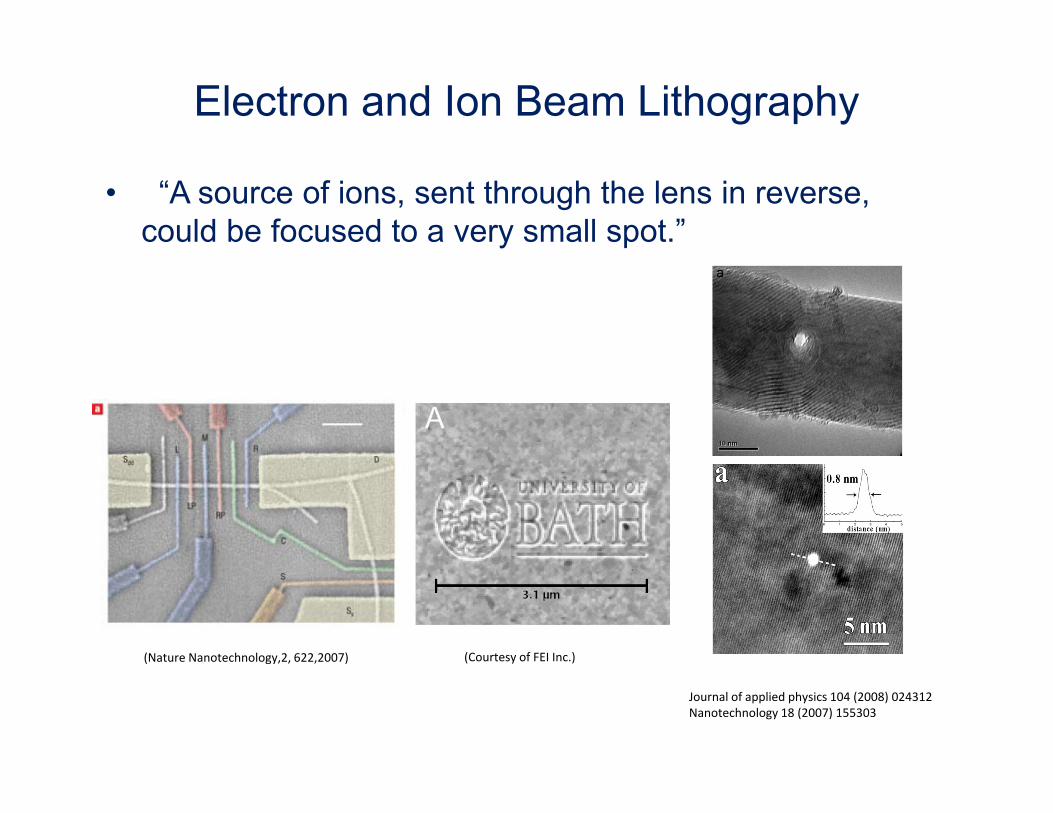
Electron and Ion Beam Lithography
• “A source of ions, sent through the lens in reverse, could be focused to a very small spot.”
(Courtesy of FEI Inc.)(Nature Nanotechnology,2, 622,2007) ( y )( gy, , , )
Journal of applied physics 104 (2008) 024312 Nanotechnology 18 (2007) 155303
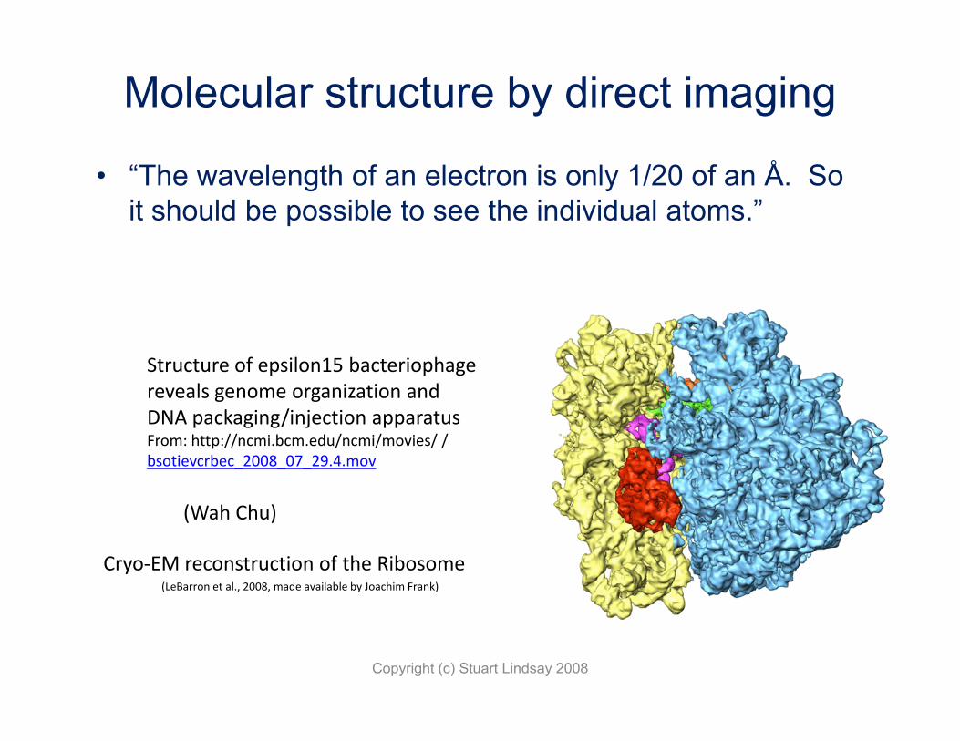
Molecular structure by direct imaging
• “The wavelength of an electron is only 1/20 of an Å. So it should be possible to see the individual atoms.”
Structure of epsilon15 bacteriophagereveals genome organization and DNA packaging/injection apparatusDNA packaging/injection apparatus From: http://ncmi.bcm.edu/ncmi/movies/ /bsotievcrbec_2008_07_29.4.mov
(Wah Chu)
Cryo‐EM reconstruction of the Ribosome(LeBarron et al., 2008, made available by Joachim Frank)
(Wah Chu)
Copyright (c) Stuart Lindsay 2008
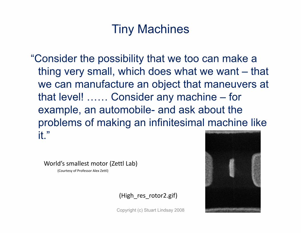
Tiny Machines
“Consider the possibility that we too can make a thing very small which does what we want – thatthing very small, which does what we want that we can manufacture an object that maneuvers at that level! …… Consider any machine – for yexample, an automobile- and ask about the problems of making an infinitesimal machine like i ”it.”
World’s smallest motor (Zettl Lab)(Courtesy of Professor Alex Zettl)
(High_res_rotor2.gif)
Copyright (c) Stuart Lindsay 2008
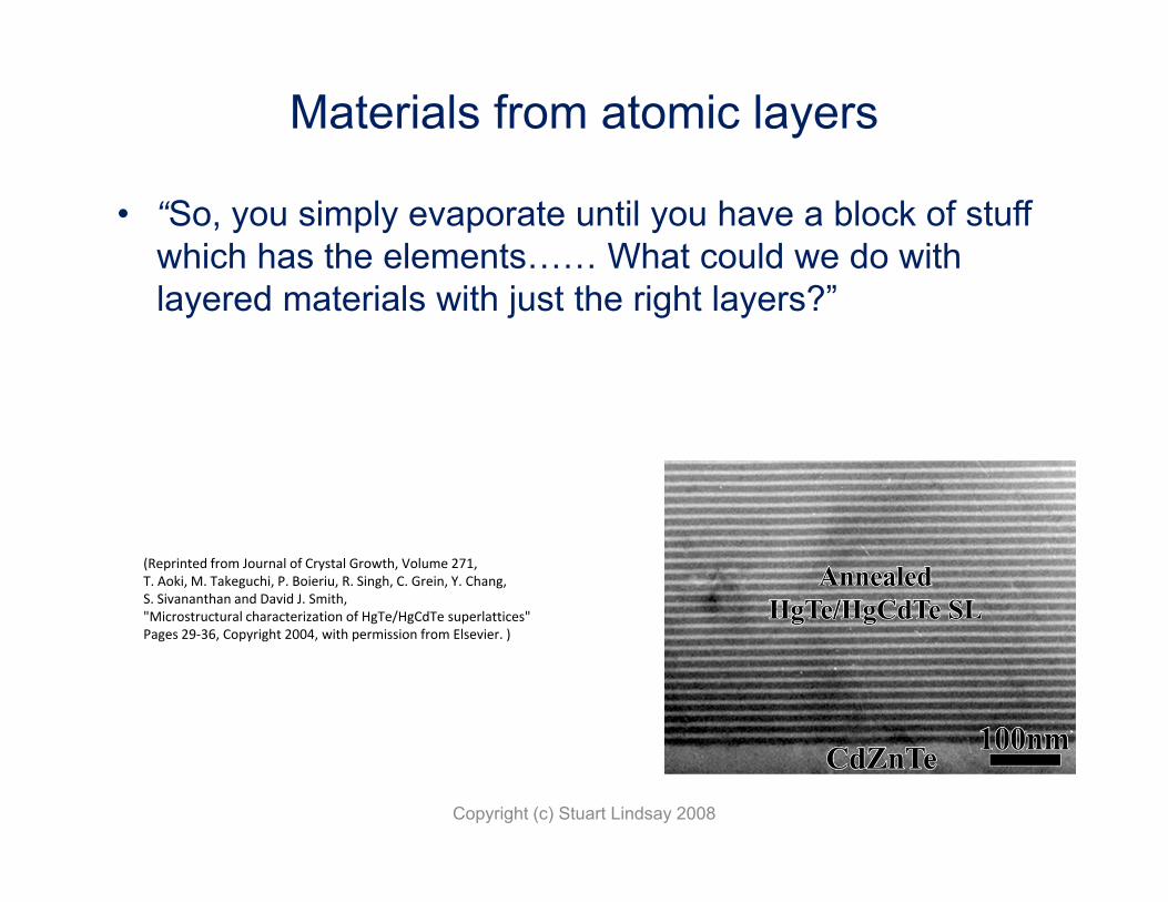
Materials from atomic layers
• “So, you simply evaporate until you have a block of stuff which has the elements…… What could we do with layered materials with just the right layers?”
(Reprinted from Journal of Crystal Growth, Volume 271, T. Aoki, M. Takeguchi, P. Boieriu, R. Singh, C. Grein, Y. Chang, S. Sivananthan and David J. Smith, "Microstructural characterization of HgTe/HgCdTe superlattices" g / g pPages 29‐36, Copyright 2004, with permission from Elsevier. )
Copyright (c) Stuart Lindsay 2008
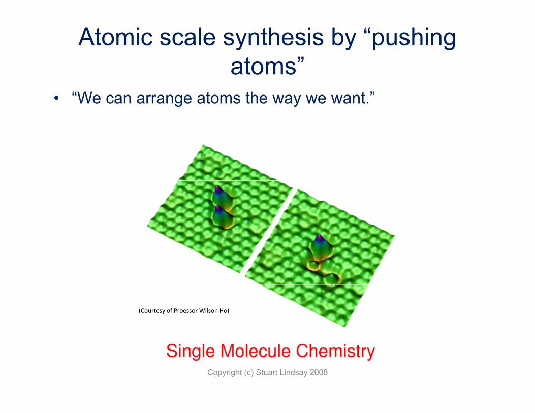
Atomic scale synthesis by “pushing atoms”
• “We can arrange atoms the way we want.”
(Courtesy of Proessor Wilson Ho)
Copyright (c) Stuart Lindsay 2008
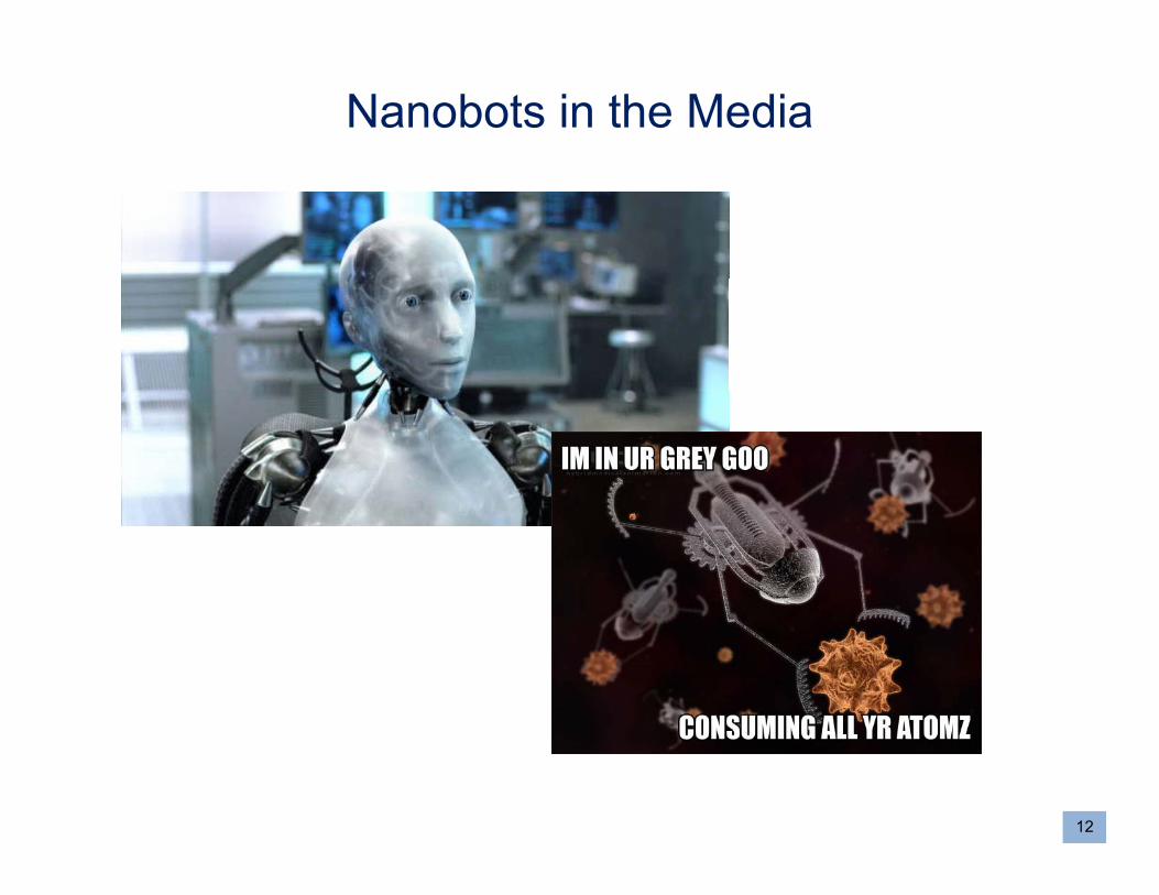
Nanobots in the Media
12
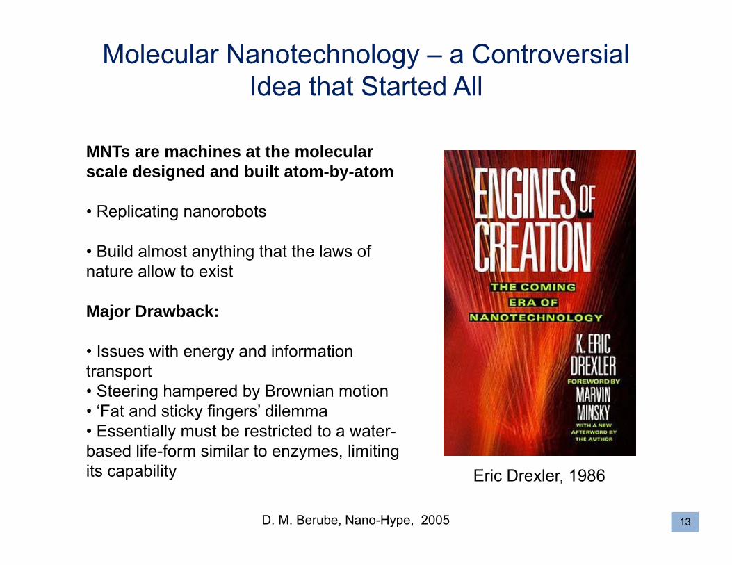
Molecular Nanotechnology – a Controversial Idea that Started All
MNTs are machines at the molecular scale designed and built atom-by-atomscale designed and built atom by atom
• Replicating nanorobots
B ild l t thi th t th l f• Build almost anything that the laws of nature allow to exist
Major Drawback:j
• Issues with energy and information transport• Steering hampered by Brownian motion• Steering hampered by Brownian motion• ‘Fat and sticky fingers’ dilemma• Essentially must be restricted to a water-based life-form similar to enzymes, limiting
13
its capability Eric Drexler, 1986
D. M. Berube, Nano-Hype, 2005

I N H ?Is Nano a Hype?
14
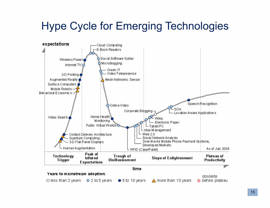
Hype Cycle for Emerging Technologies
15
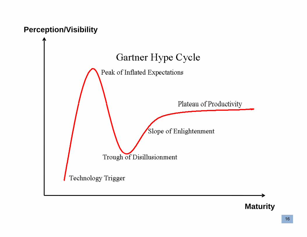
Perception/Visibility
16
Maturity
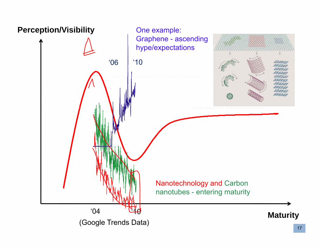
Perception/Visibility One example:Graphene - ascending h / t tihype/expectations
‘06 ‘10
Nanotechnology and Carbon nanotubes - entering maturity
17
Maturity(Google Trends Data)
‘10‘04
A Real-World Example of Nanoscience Principles:
C t T h lComputer Technology
18
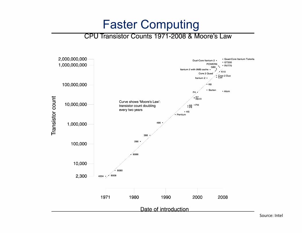
Faster Computing
Source: Intel
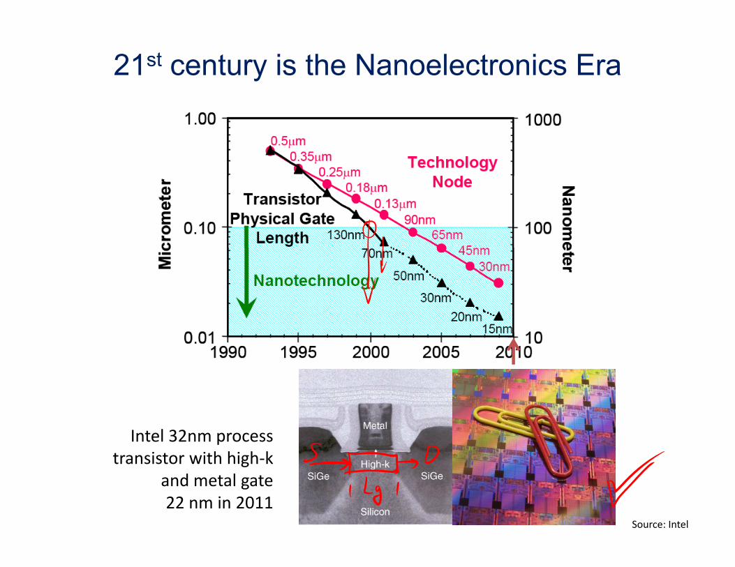
21st century is the Nanoelectronics Era
Intel 32nm process transistor with high‐k
Source: Intel
transistor with high k and metal gate22 nm in 2011
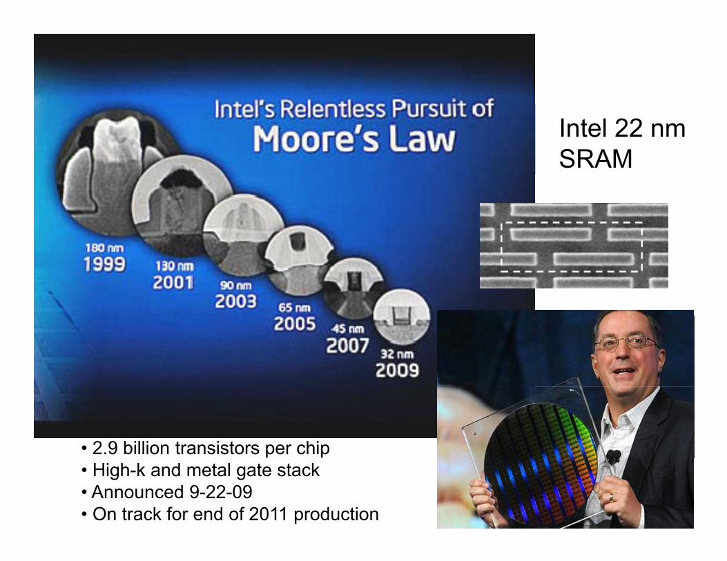
Intel 22 nmSRAM
• 2.9 billion transistors per chip
21
p p• High-k and metal gate stack • Announced 9-22-09• On track for end of 2011 production
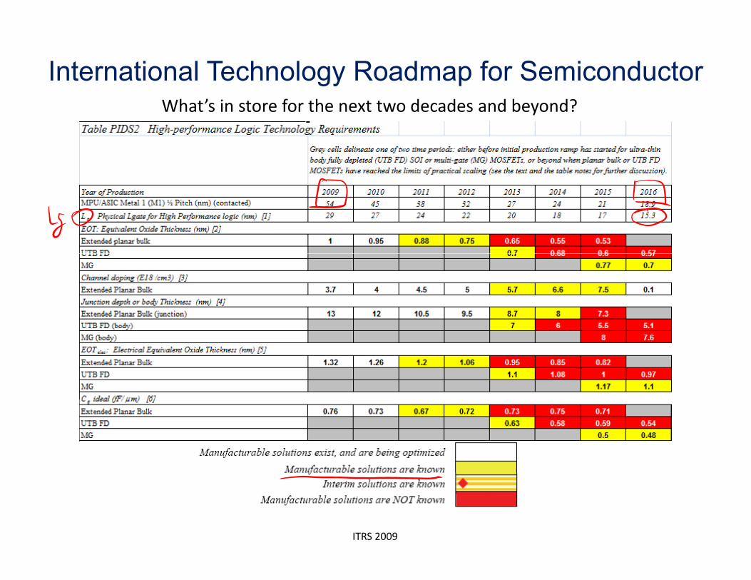
International Technology Roadmap for SemiconductorWhat’s in store for the next two decades and beyond?What s in store for the next two decades and beyond?
ITRS 2009
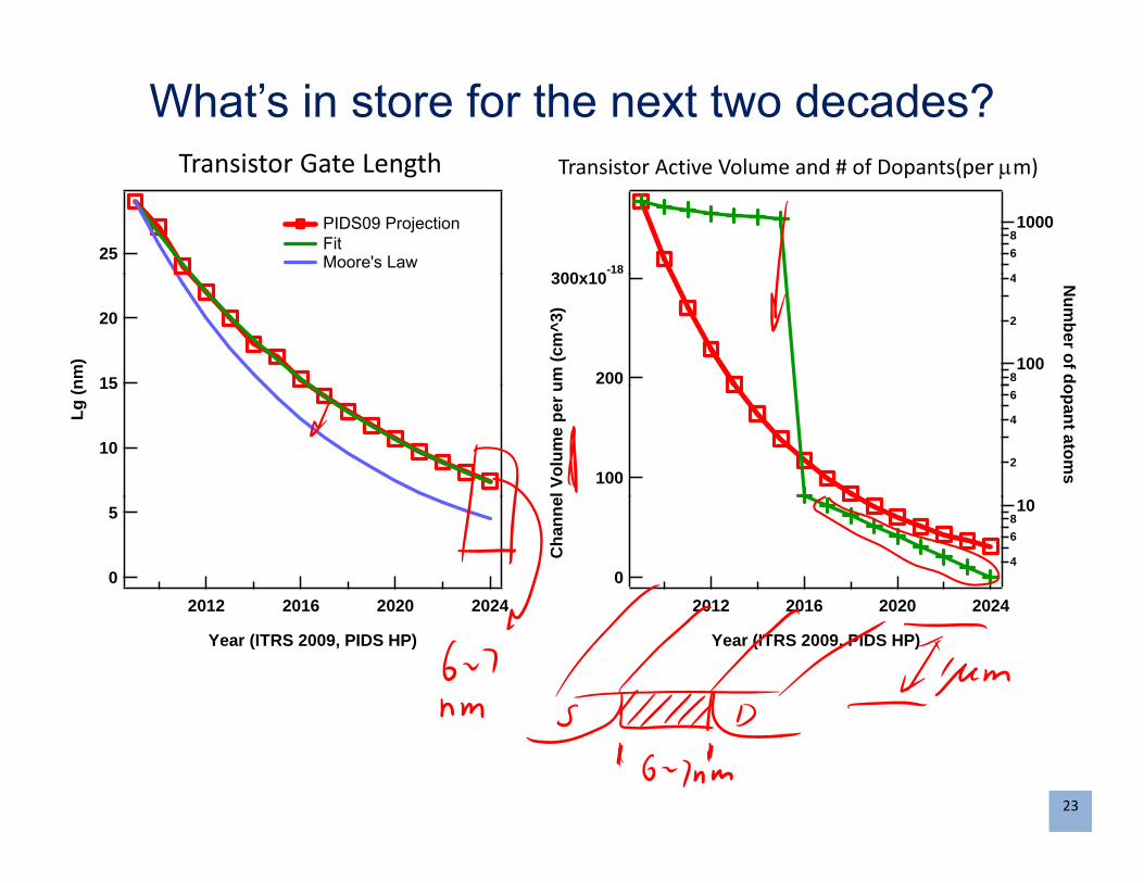
What’s in store for the next two decades?Transistor Gate Length Transistor Active Volume and # of Dopants(per m)
25
PIDS09 Projection Fit Moore's Law
300 10-184
681000
Transistor Gate Length Transistor Active Volume and # of Dopants(per m)
20
15nm)
300x10
200um (c
m^3
)
8100
2
4 Num
ber of do15
10
Lg (n
100
l Vol
ume
per u
2
4
6
opant atoms
5
02024202020162012
0C
hann
e
2024202020162012
4
6810
2024202020162012
Year (ITRS 2009, PIDS HP)
2024202020162012
Year (ITRS 2009, PIDS HP)
23
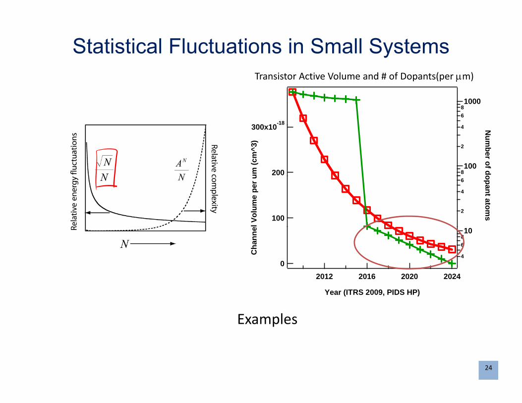
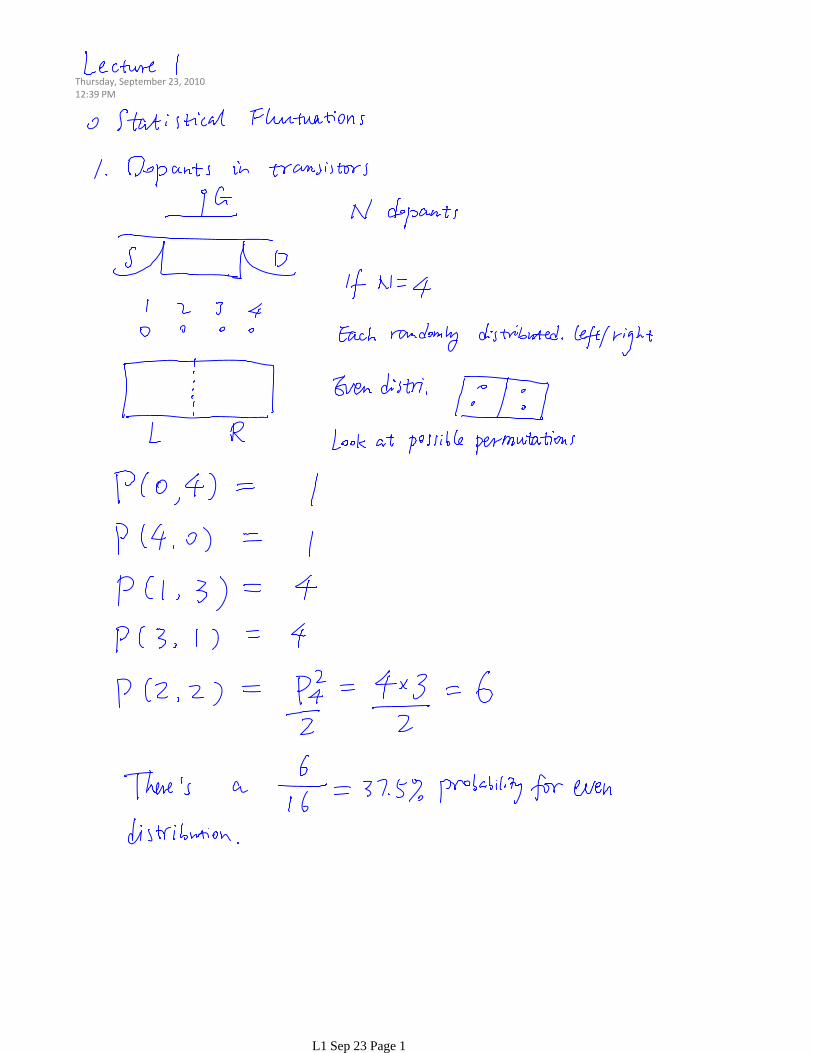
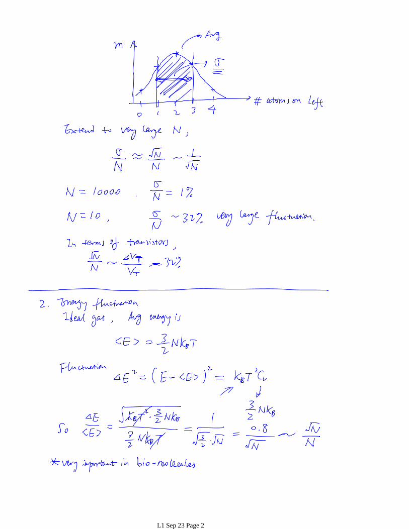
Statistical Fluctuations in Small SystemsTransistor Active Volume and # of Dopants(per m)
300 10-184
681000
Transistor Active Volume and # of Dopants(per m)
300x10
200um (c
m^3
)
8100
2
4 Num
ber of do
100
l Vol
ume
per u
2
4
6
opant atoms
0C
hann
e
2024202020162012
4
6810
2024202020162012
Year (ITRS 2009, PIDS HP)
Examples
24
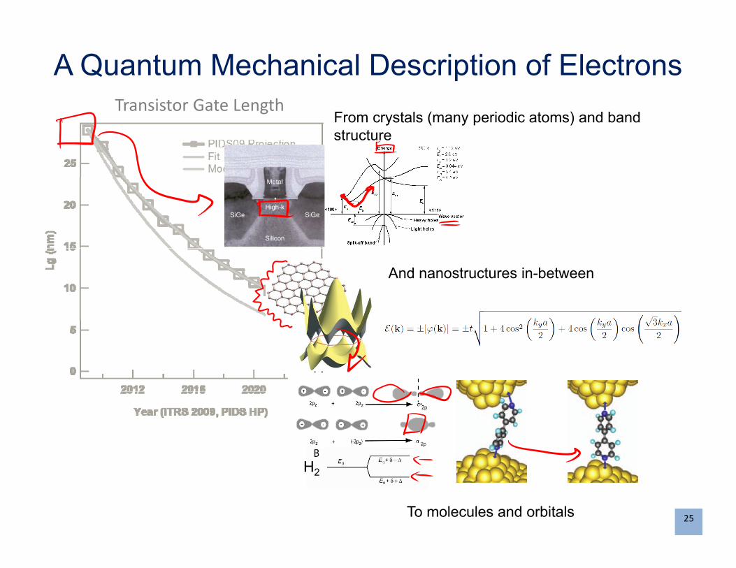
A Quantum Mechanical Description of ElectronsTransistor Gate LengthTransistor Gate Length
From crystals (many periodic atoms) and band structure
And nanostructures in-between
H
25To molecules and orbitals
H2
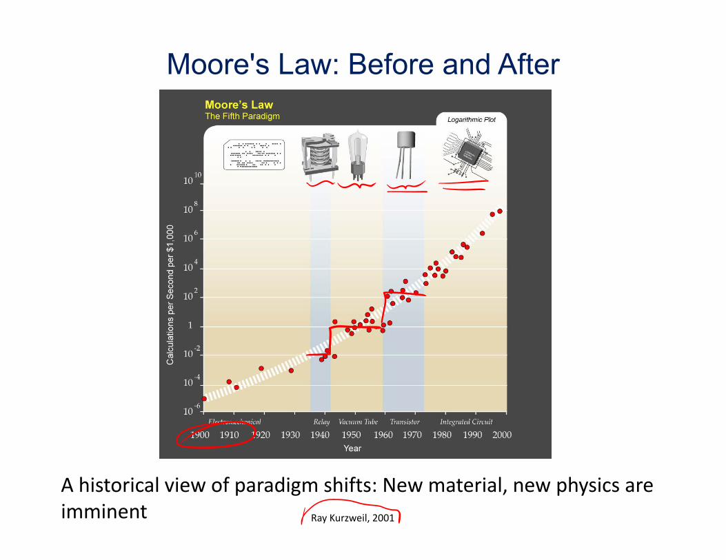
Moore's Law: Before and After
Ray Kurzweil, 2001
A historical view of paradigm shifts: New material, new physics are imminent
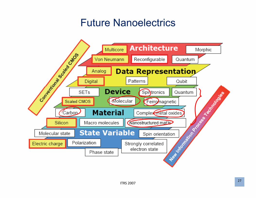
Future Nanoelectrics
27ITRS 2007
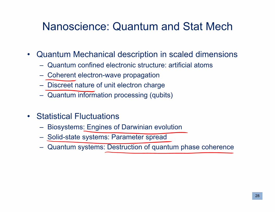
Nanoscience: Quantum and Stat Mech
• Quantum Mechanical description in scaled dimensions– Quantum confined electronic structure: artificial atomsQuantum confined electronic structure: artificial atoms– Coherent electron-wave propagation– Discreet nature of unit electron charge
Q t i f ti i ( bit )– Quantum information processing (qubits)
• Statistical Fluctuations– Biosystems: Engines of Darwinian evolution– Solid-state systems: Parameter spread
Quantum systems: Destruction of quantum phase coherence– Quantum systems: Destruction of quantum phase coherence
28
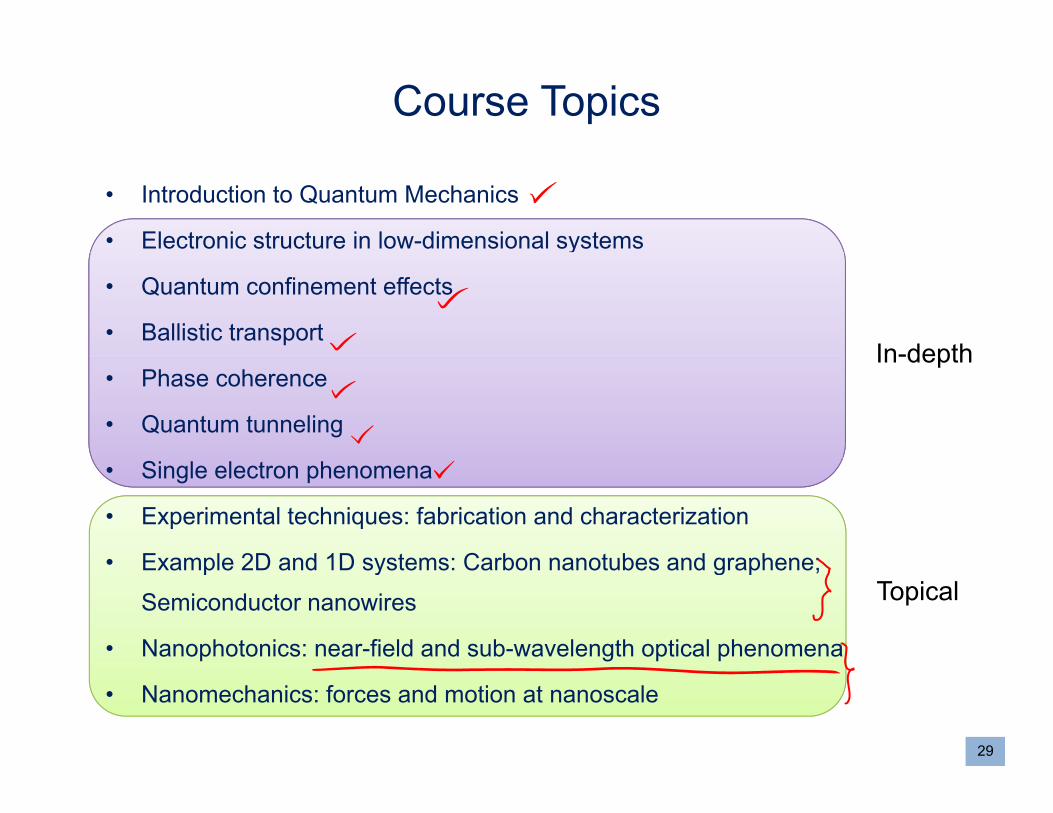
Course Topics
• Introduction to Quantum Mechanics
• Electronic structure in low-dimensional systemsy
• Quantum confinement effects
• Ballistic transportIn-depth
• Phase coherence
• Quantum tunneling
In-depth
• Single electron phenomena
• Experimental techniques: fabrication and characterization
• Example 2D and 1D systems: Carbon nanotubes and graphene;• Example 2D and 1D systems: Carbon nanotubes and graphene;
Semiconductor nanowires
• Nanophotonics: near-field and sub-wavelength optical phenomena
Topical
• Nanomechanics: forces and motion at nanoscale
29
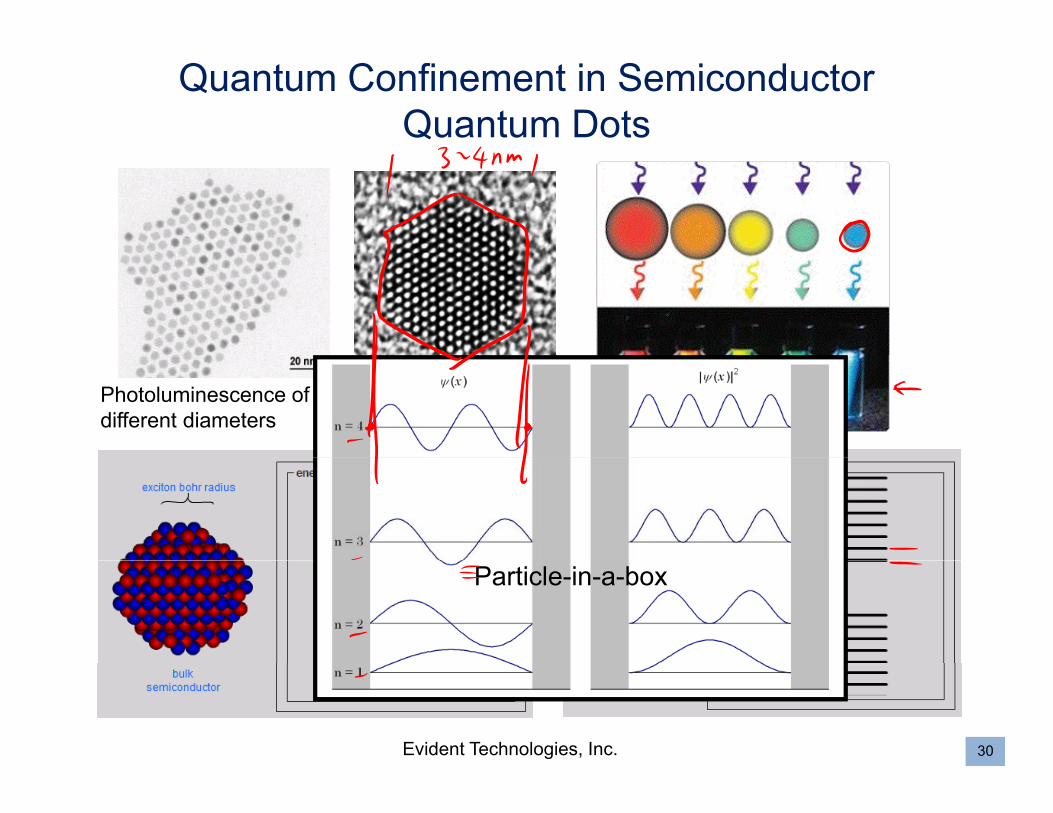
Quantum Confinement in Semiconductor Quantum Dots
Photoluminescence of CdSe nanocrystals of different diameters
Particle-in-a-box
30Evident Technologies, Inc.
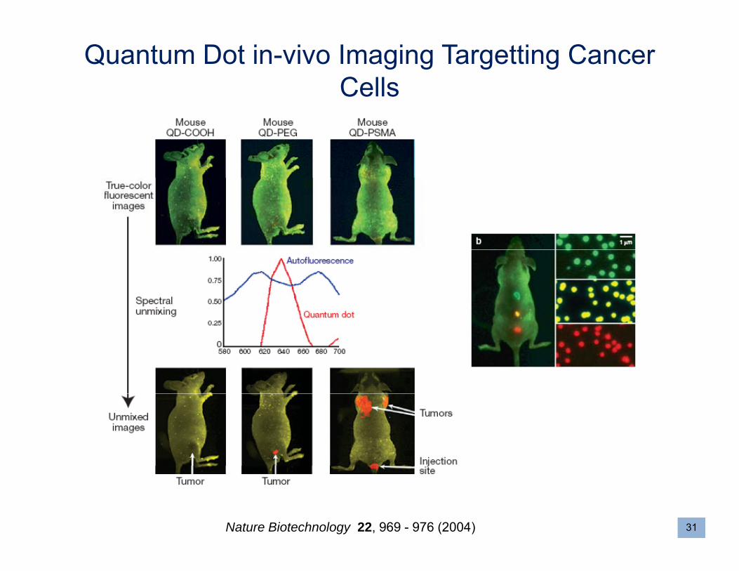
Quantum Dot in-vivo Imaging Targetting Cancer Cells
31Nature Biotechnology 22, 969 - 976 (2004)
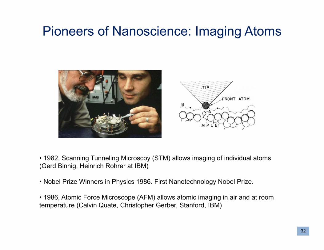
Pioneers of Nanoscience: Imaging Atoms
• 1982, Scanning Tunneling Microscoy (STM) allows imaging of individual atoms (Gerd Binnig, Heinrich Rohrer at IBM)
• Nobel Prize Winners in Physics 1986. First Nanotechnology Nobel Prize.
• 1986, Atomic Force Microscope (AFM) allows atomic imaging in air and at room temperat re (Cal in Q ate Christopher Gerber Stanford IBM)
32
temperature (Calvin Quate, Christopher Gerber, Stanford, IBM)
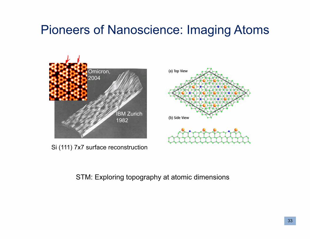
Pioneers of Nanoscience: Imaging Atoms
Omicron,2004
IBM Zurich1982
Si (111) 7x7 surface reconstruction
STM: Exploring topography at atomic dimensions
33
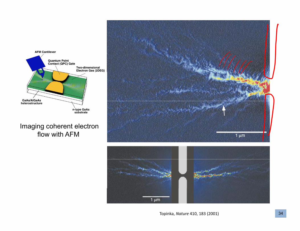
Imaging coherent electron flow with AFM
34Topinka, Nature 410, 183 (2001)
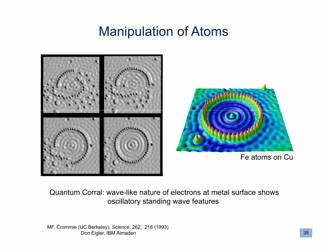
Manipulation of Atoms
Fe atoms on Cu
Quantum Corral: wave-like nature of electrons at metal surface shows oscillatory standing wave features
35MF. Crommie (UC Berkeley), Science, 262, 218 (1993)
Don Eigler, IBM Almaden
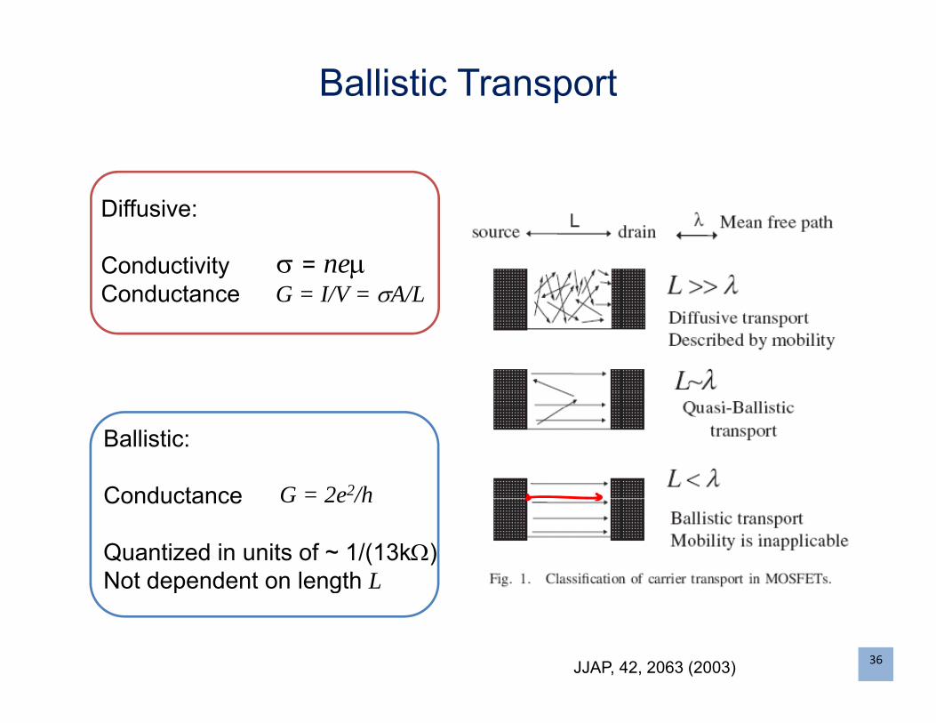
Ballistic Transport
Diffusive:
ConductivityConductance
= neG = I/V = A/L
Ballistic:
Conductance G = 2e2/hConductance
Quantized in units of ~ 1/(13k)Not dependent on length L
G 2e /h
36JJAP, 42, 2063 (2003)
p g
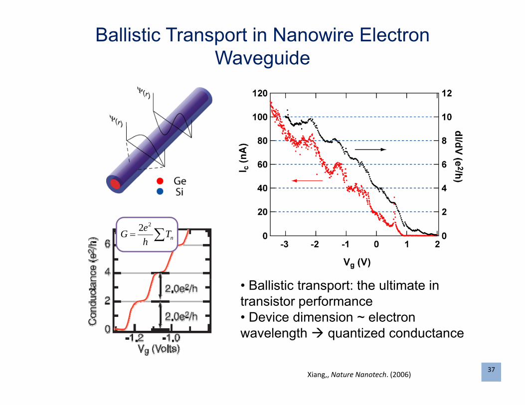
Ballistic Transport in Nanowire Electron Waveguide
e22 nTheG 2
• Ballistic transport: the ultimate in transistor performance• Device dimension ~ electron
l th ti d d t
37Xiang,, Nature Nanotech. (2006)
wavelength quantized conductance
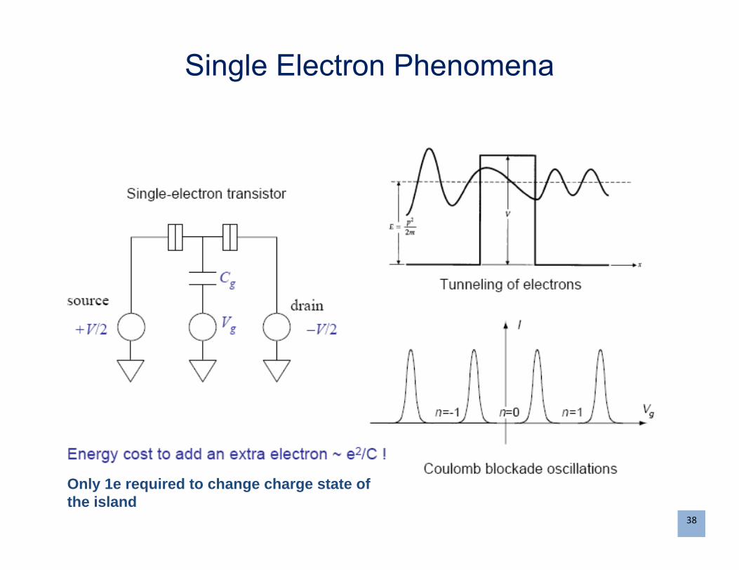
Single Electron Phenomena
38
Only 1e required to change charge state of the island
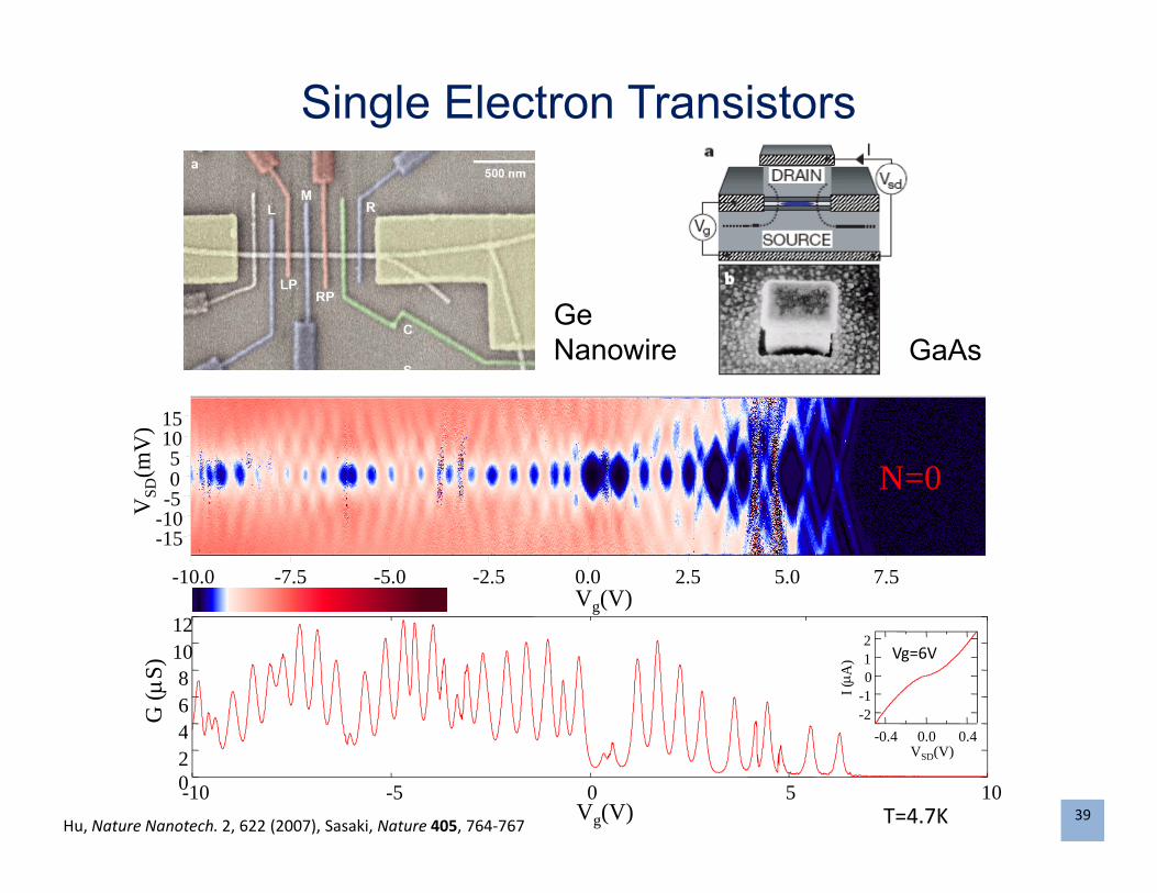
Single Electron Transistors
GeNanowire GaAs
N=0
151050
-5VSD
(mV
)
-10.0 -7.5 -5.0 -2.5 0.0 2.5 5.0 7.5
5-10-15
V
Vg(V)
I( A
)
-2-1012
Vg=6V1210864
G (
S)
39Vg(V)
-0.4 0.0 0.4VSD(V)
420-10 -5 0 5 10
T=4.7KHu, Nature Nanotech. 2, 622 (2007), Sasaki, Nature 405, 764‐767
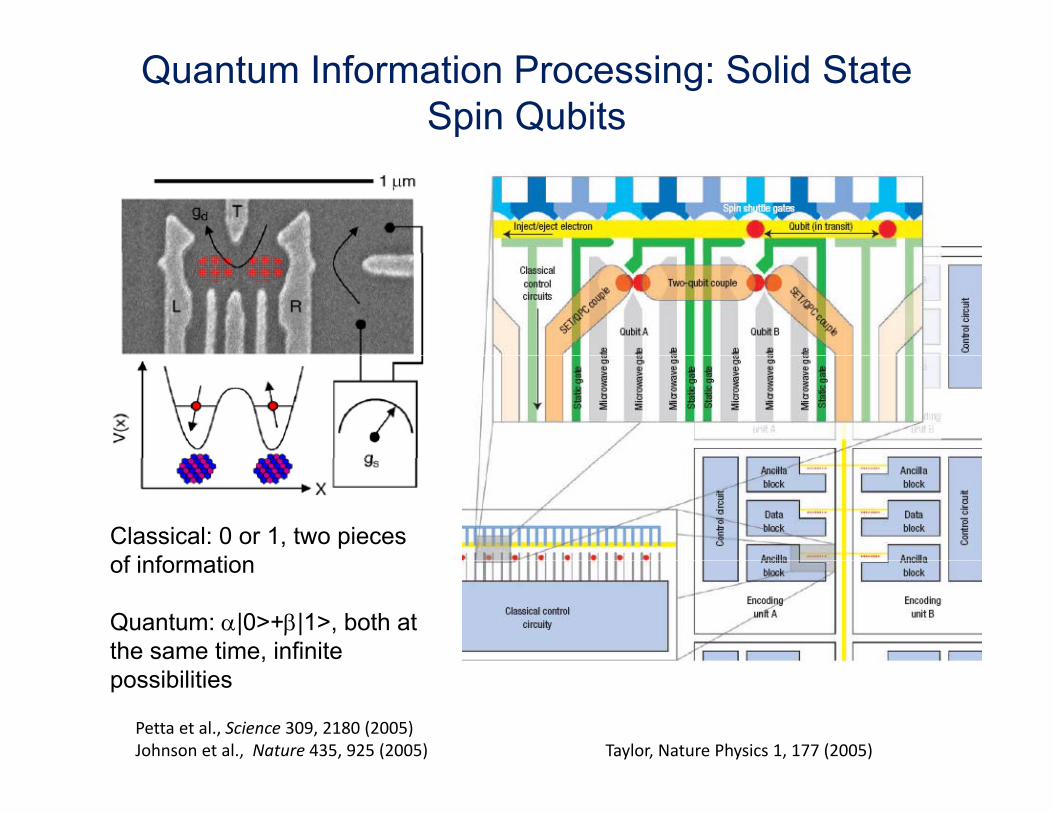
Quantum Information Processing: Solid State Spin Qubits
Classical: 0 or 1, two pieces of informationof information
Quantum: |0>+|1>, both at the same time, infinite
Petta et al., Science 309, 2180 (2005)Johnson et al., Nature 435, 925 (2005) Taylor, Nature Physics 1, 177 (2005)
possibilities
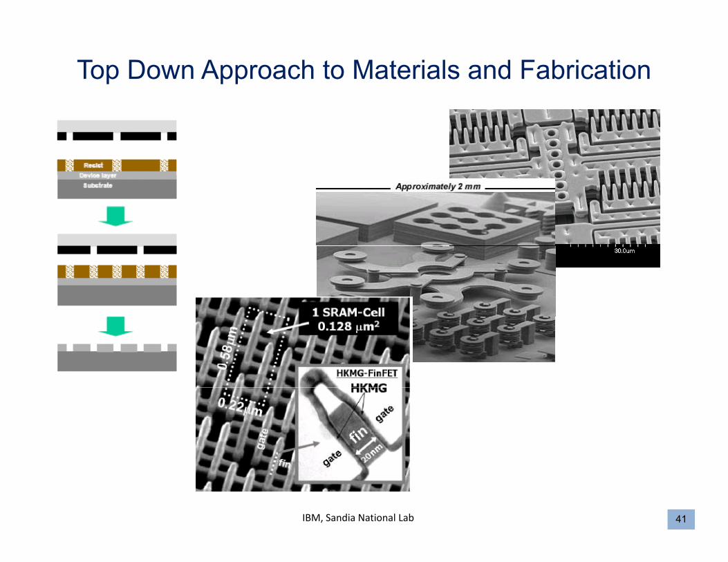
Top Down Approach to Materials and Fabrication
41IBM, Sandia National Lab
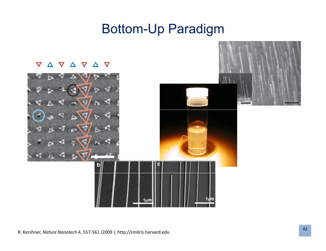
Bottom-Up Paradigm
42R. Kershner, Nature Nanotech 4, 557‐561 (2009 ), http://cmliris.harvard.edu
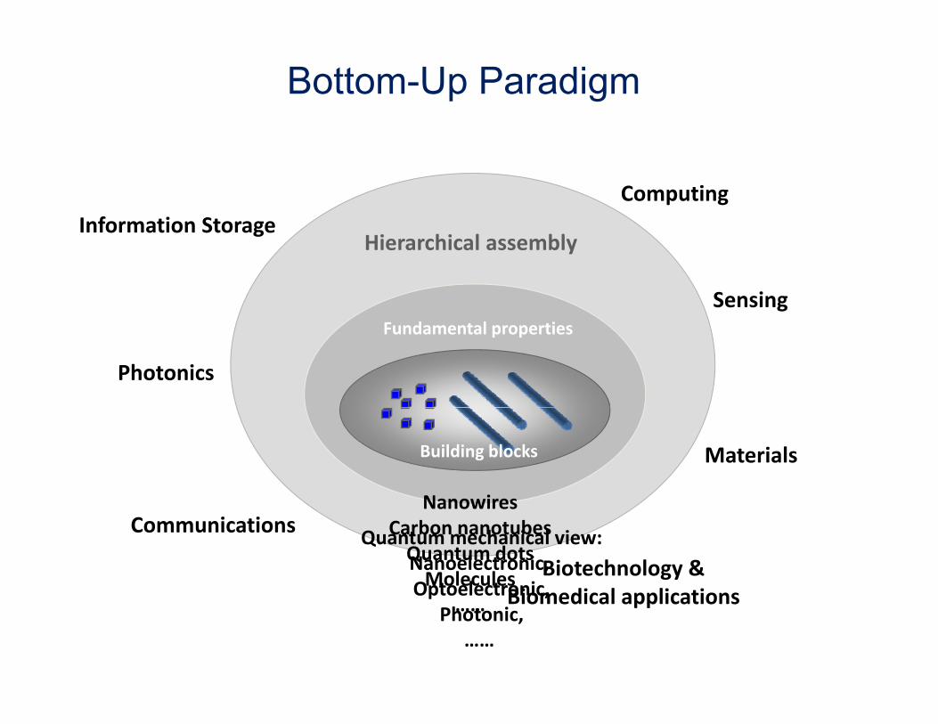
Bottom-Up Paradigm
Information StorageComputing
Hierarchical assemblyInformation Storage
SensingFundamental properties
Photonics
Building blocks
Nanowires
Materials
NanowiresCarbon nanotubesQuantum dotsMolecules
Quantum mechanical view:Nanoelectronic, Optoelectronic
Biotechnology &Bi di l li ti
Communications
……Optoelectronic,
Photonic,……
Biomedical applications
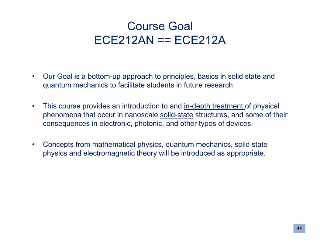
Course GoalECE212AN == ECE212A
• Our Goal is a bottom-up approach to principles basics in solid state and• Our Goal is a bottom-up approach to principles, basics in solid state and quantum mechanics to facilitate students in future research
• This course provides an introduction to and in-depth treatment of physicalThis course provides an introduction to and in depth treatment of physical phenomena that occur in nanoscale solid-state structures, and some of their consequences in electronic, photonic, and other types of devices.
• Concepts from mathematical physics, quantum mechanics, solid state physics and electromagnetic theory will be introduced as appropriate.
44

Course Schedule• Lectures: Tu Th 12:30a - 1:50p• Location: TM 102
Webpage:http://ece-classweb.ucsd.edu/fall10/ece212an/
InstructorP f Ji Xi
Teaching Fellow• Prof. Jie Xiang• Email: [email protected]• Phone: x27659
• Han-Ping Chen• Email: [email protected]• Phone: x20951
• Office: EBU-1 3208• Office hours: Thursdays 2:00 ~ 3:30
PM or by appointment
• Office: EBU-1 3710• Office hours: tba
4545
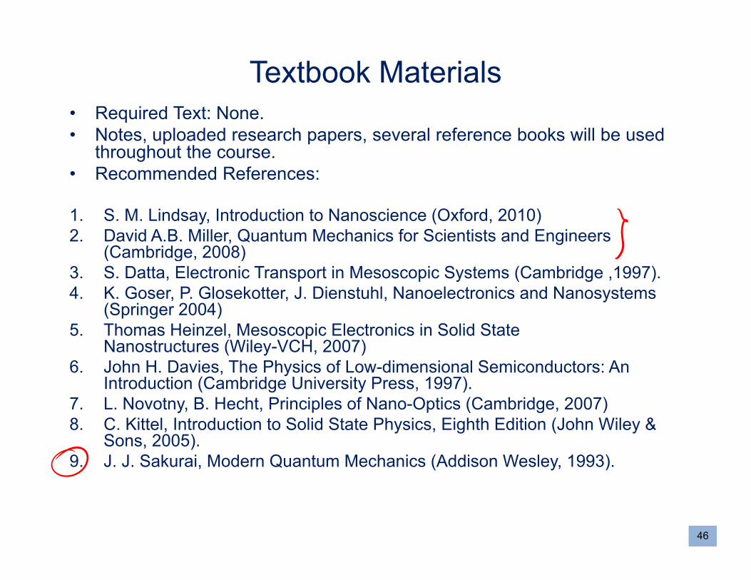
Textbook MaterialsR i d T t N• Required Text: None.
• Notes, uploaded research papers, several reference books will be used throughout the course.
• Recommended References:
1. S. M. Lindsay, Introduction to Nanoscience (Oxford, 2010)2. David A.B. Miller, Quantum Mechanics for Scientists and Engineers
(Cambridge 2008)(Cambridge, 2008)3. S. Datta, Electronic Transport in Mesoscopic Systems (Cambridge ,1997).4. K. Goser, P. Glosekotter, J. Dienstuhl, Nanoelectronics and Nanosystems
(Springer 2004)5 Thomas Hein el Mesoscopic Electronics in Solid State5. Thomas Heinzel, Mesoscopic Electronics in Solid State
Nanostructures (Wiley-VCH, 2007)6. John H. Davies, The Physics of Low-dimensional Semiconductors: An
Introduction (Cambridge University Press, 1997).7 L N t B H ht P i i l f N O ti (C b id 2007)7. L. Novotny, B. Hecht, Principles of Nano-Optics (Cambridge, 2007)8. C. Kittel, Introduction to Solid State Physics, Eighth Edition (John Wiley &
Sons, 2005).9. J. J. Sakurai, Modern Quantum Mechanics (Addison Wesley, 1993).
46
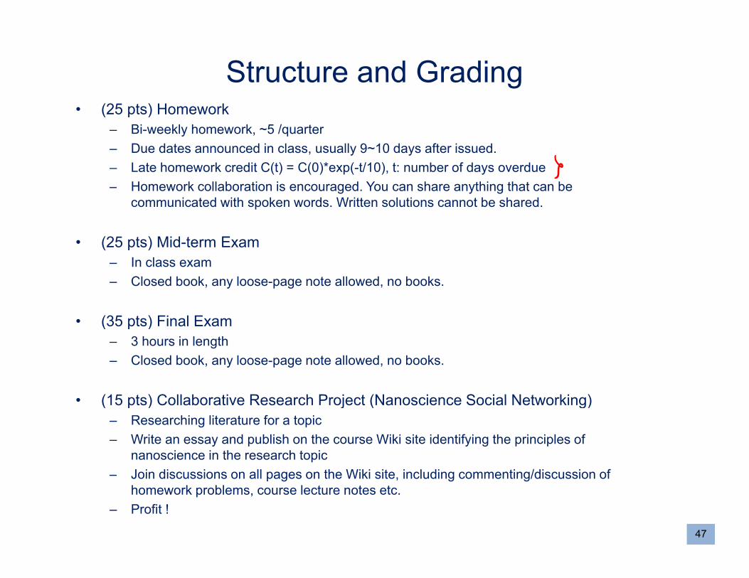
Structure and Grading(25 pts) Homework• (25 pts) Homework
– Bi-weekly homework, ~5 /quarter– Due dates announced in class, usually 9~10 days after issued. – Late homework credit C(t) = C(0)*exp(-t/10), t: number of days overdue– Homework collaboration is encouraged. You can share anything that can be
communicated with spoken words. Written solutions cannot be shared.
• (25 pts) Mid-term Exam– In class exam– Closed book, any loose-page note allowed, no books.
• (35 pts) Final Exam(35 pts) Final Exam– 3 hours in length– Closed book, any loose-page note allowed, no books.
• (15 pts) Collaborative Research Project (Nanoscience Social Networking)• (15 pts) Collaborative Research Project (Nanoscience Social Networking)– Researching literature for a topic– Write an essay and publish on the course Wiki site identifying the principles of
nanoscience in the research topicJ i di i ll th Wiki it i l di ti /di i f– Join discussions on all pages on the Wiki site, including commenting/discussion of homework problems, course lecture notes etc.
– Profit !
47
Thursday, September 23, 201012:39 PM
L1 Sep 23 Page 1
L1 Sep 23 Page 2
L1 Sep 23 Page 3