Embed Size (px)
Citation preview
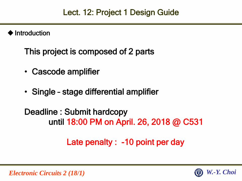
Electronic Circuits 2 (18/1) W.-Y. Choi
Lect. 12: Project 1 Design Guide
Introduction
This project is composed of 2 parts
• Cascode amplifier
• Single – stage differential amplifier
Deadline : Submit hardcopy
until 18:00 PM on April. 26, 2018 @ C531
Late penalty : -10 point per day
Electronic Circuits 2 (18/1) W.-Y. Choi
Lect. 12: Project 1 Design Guide
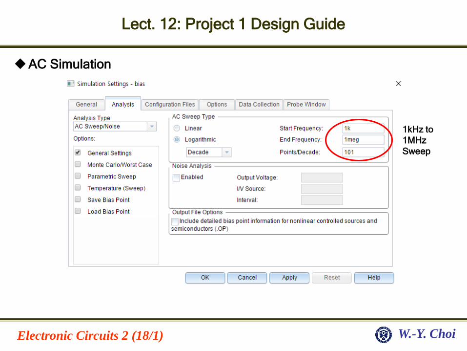
AC Simulation
1kHz to
1MHz
Sweep
Electronic Circuits 2 (18/1) W.-Y. Choi
Lect. 12: Project 1 Design Guide
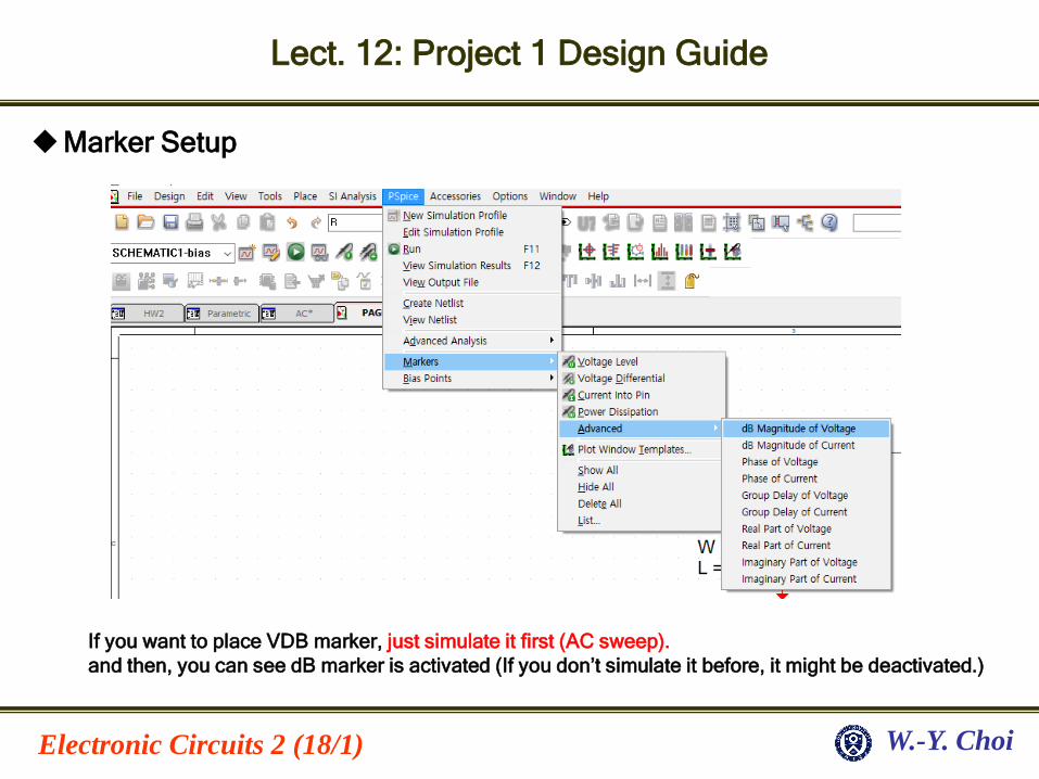
Marker Setup
If you want to place VDB marker, just simulate it first (AC sweep).
and then, you can see dB marker is activated (If you don’t simulate it before, it might be deactivated.)
Electronic Circuits 2 (18/1) W.-Y. Choi
Lect. 12: Project 1 Design Guide
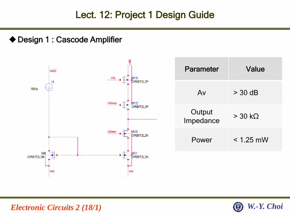
Design 1 : Cascode Amplifier
Parameter Value
Av > 30 dB
Output
Impedance> 30 kΩ
Power < 1.25 mW
Electronic Circuits 2 (18/1) W.-Y. Choi
Lect. 12: Project 1 Design Guide
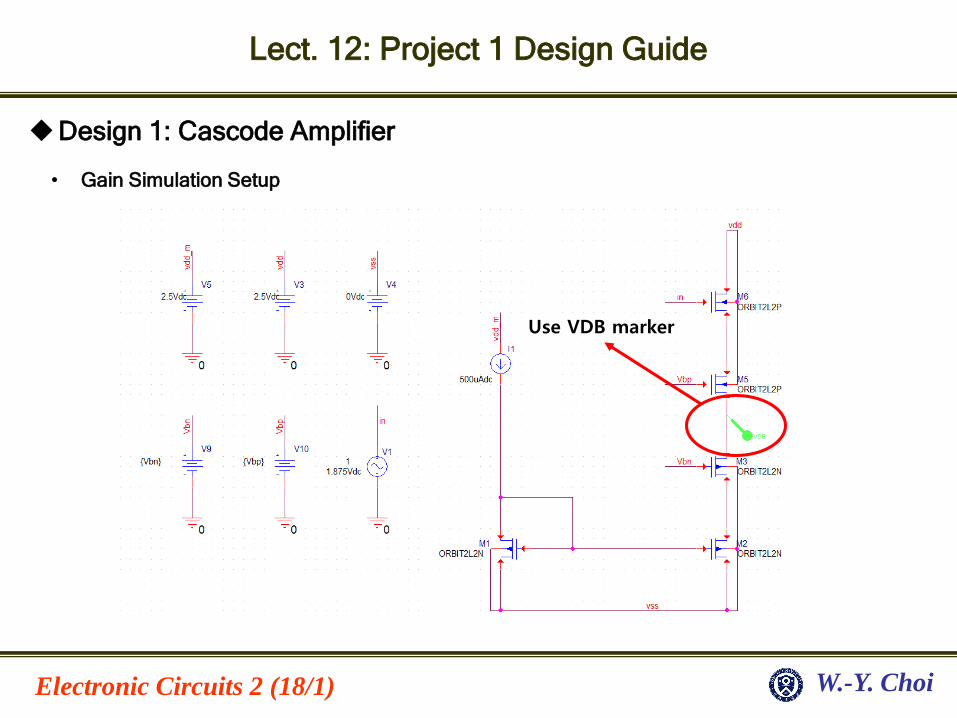
Design 1: Cascode Amplifier
• Gain Simulation Setup
Use VDB marker
Electronic Circuits 2 (18/1) W.-Y. Choi
Lect. 12: Project 1 Design Guide
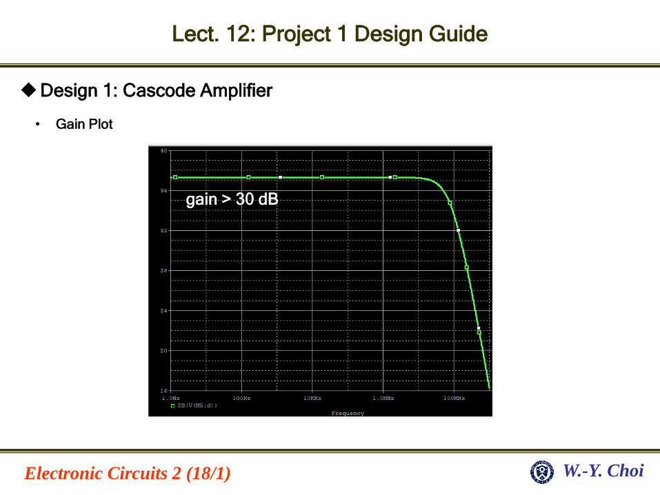
Design 1: Cascode Amplifier
• Gain Plot
gain > 30 dB
Electronic Circuits 2 (18/1) W.-Y. Choi
Lect. 12: Project 1 Design Guide
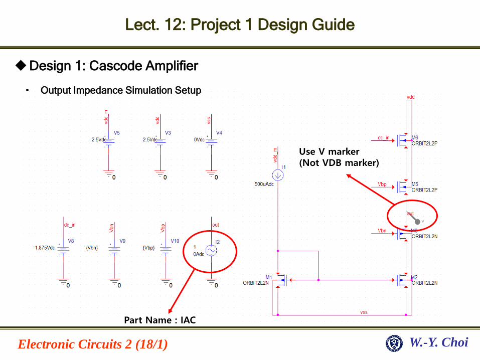
Design 1: Cascode Amplifier
Part Name : IAC
Use V marker (Not VDB marker)
• Output Impedance Simulation Setup
Electronic Circuits 2 (18/1) W.-Y. Choi
Lect. 12: Project 1 Design Guide
Design 1: Cascode Amplifier
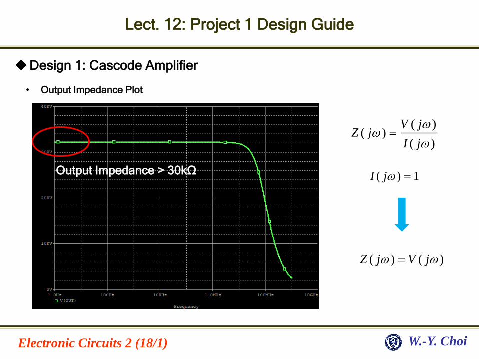
• Output Impedance Plot
( )( )
( )
V jZ j
I j
( ) 1I j
( ) ( )Z j V j
Output Impedance > 30kΩ
Electronic Circuits 2 (18/1) W.-Y. Choi
Lect. 12: Project 1 Design Guide
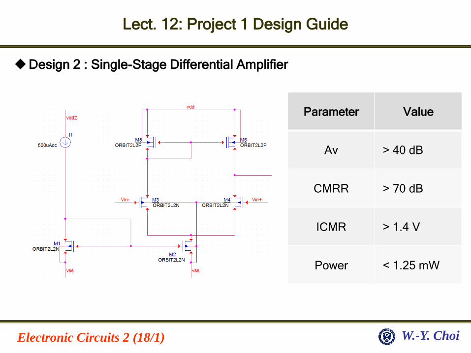
Design 2 : Single-Stage Differential Amplifier
Parameter Value
Av > 40 dB
CMRR > 70 dB
ICMR > 1.4 V
Power < 1.25 mW
Electronic Circuits 2 (18/1) W.-Y. Choi
Lect. 12: Project 1 Design Guide
Design 2 : Single-Stage Differential Amplifier
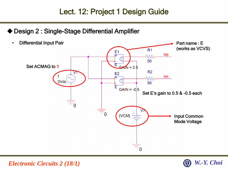
Part name : E
(works as VCVS)
Input Common
Mode Voltage
Set ACMAG to 1
Set E’s gain to 0.5 & -0.5 each
• Differential Input Pair
Electronic Circuits 2 (18/1) W.-Y. Choi
Lect. 12: Project 1 Design Guide
Design 2 : Single-Stage Differential Amplifier
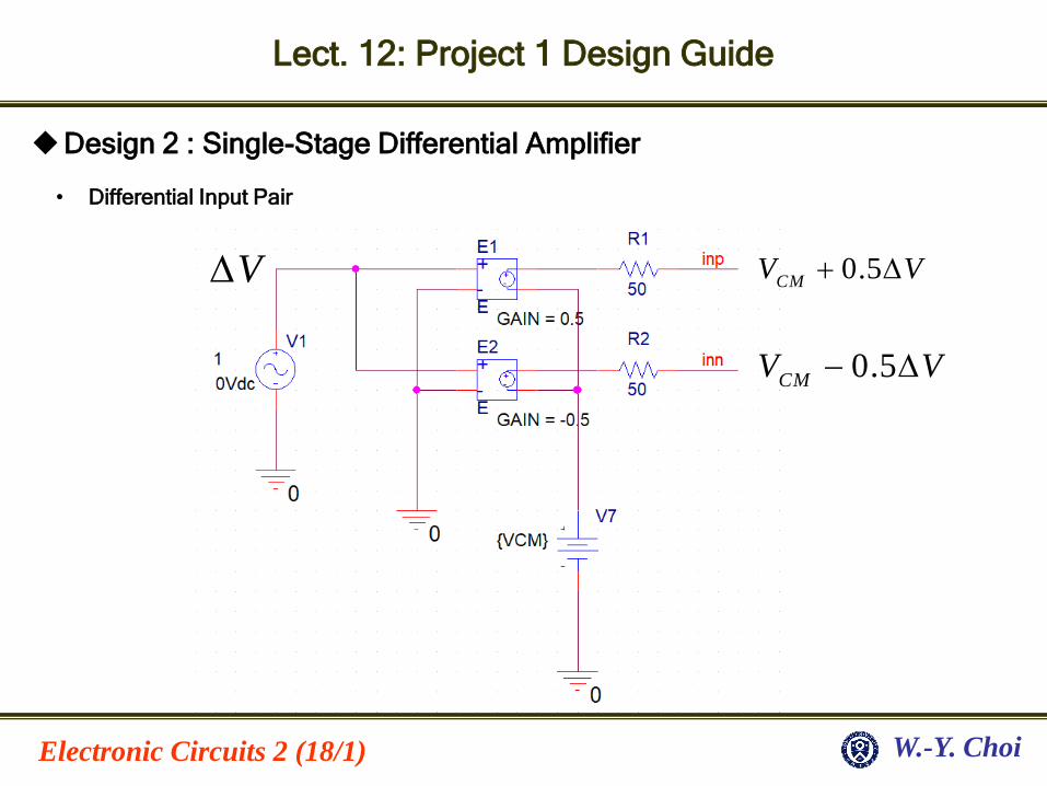
• Differential Input Pair
V 0.5CM
V V
0.5CM
V V
Electronic Circuits 2 (18/1) W.-Y. Choi
Lect. 12: Project 1 Design Guide
Design 2 : Single-Stage Differential Amplifier
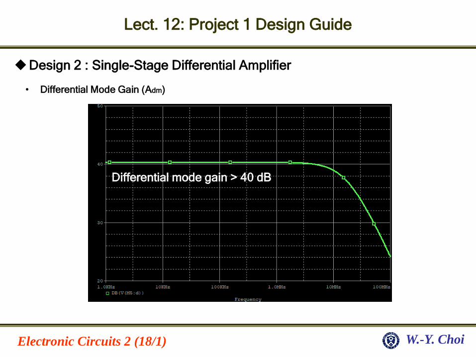
• Differential Mode Gain (Adm)
Differential mode gain > 40 dB
Electronic Circuits 2 (18/1) W.-Y. Choi
Lect. 12: Project 1 Design Guide
Design 2 : Single-Stage Differential Amplifier
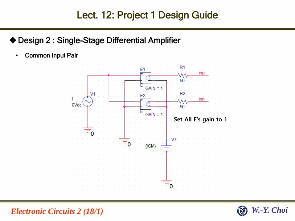
• Common Input Pair
Set All E’s gain to 1
Electronic Circuits 2 (18/1) W.-Y. Choi
Lect. 12: Project 1 Design Guide
Design 2 : Single-Stage Differential Amplifier
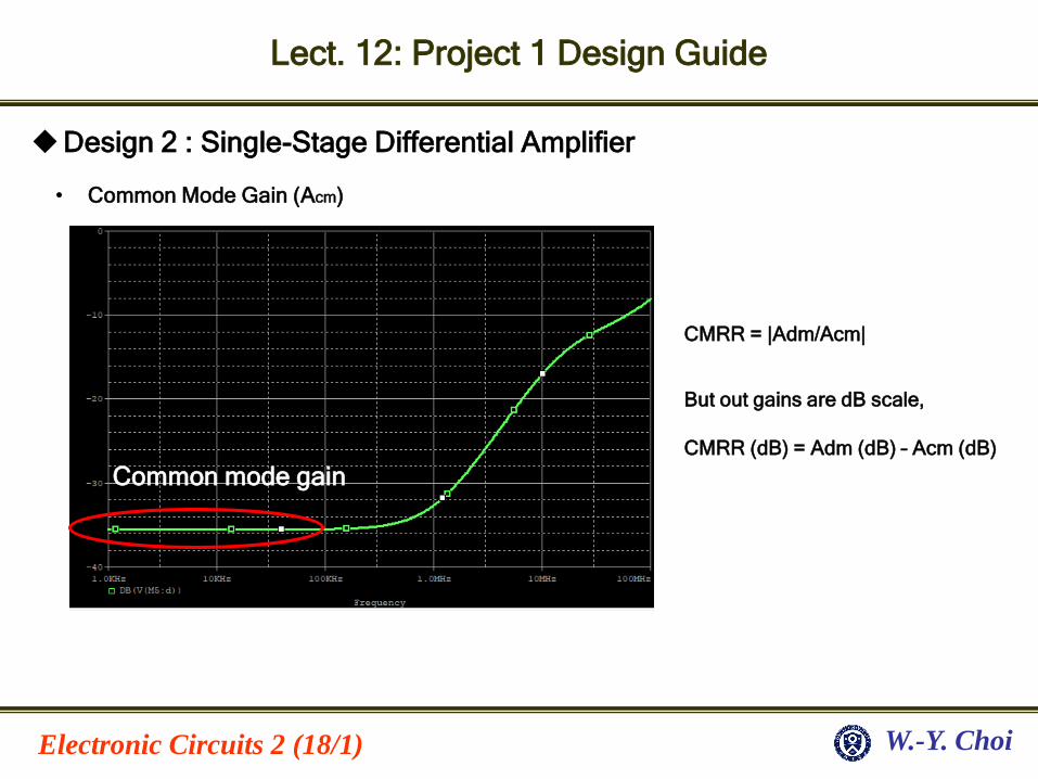
• Common Mode Gain (Acm)
Common mode gain
CMRR = |Adm/Acm|
But out gains are dB scale,
CMRR (dB) = Adm (dB) – Acm (dB)
Electronic Circuits 2 (18/1) W.-Y. Choi
Lect. 12: Project 1 Design Guide
Design 2 : Single-Stage Differential Amplifier
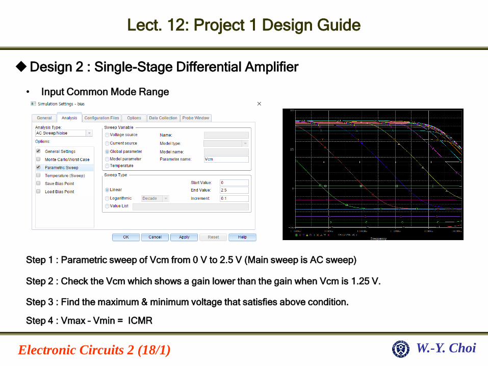
Step 1 : Parametric sweep of Vcm from 0 V to 2.5 V (Main sweep is AC sweep)
Step 2 : Check the Vcm which shows a gain lower than the gain when Vcm is 1.25 V.
Step 3 : Find the maximum & minimum voltage that satisfies above condition.
Step 4 : Vmax – Vmin = ICMR
• Input Common Mode Range
Electronic Circuits 2 (18/1) W.-Y. Choi
Lect. 12: Project 1 Design Guide
Grading Policy
• Cascode Amplifier [25], Single-Stage Differential Amplifier [25], Design Report [50]
• 5 extra point will be given for up to three designs for each part that satisfy all the specification and
produce the highest gain per power (Gain/Power)
• Best designs will be selected from Part I and II each and their designers will be given opportunities
to present their results for 5 extra point (optional)
• All plots I showed you in this lecture must be in your design report. And your design report must have
the method of design each circuit to satisfy specification and the comparison between the simulation
result and analytical solution you learned in class. Report must be written in English.
• Late penalty is -10 point per day.


![Ddi. 1 [lect.] df 0 categories of design](https://img.pdfslide.us/doc/110x75/5561e44ad8b42a9d068b4c9c/ddi-1-lect-df-0-categories-of-design.jpg)