Embed Size (px)
Citation preview
Subscriber access provided by Georgia Tech Library
ACS Nano is published by the American Chemical Society. 1155 Sixteenth StreetN.W., Washington, DC 20036Published by American Chemical Society. Copyright © American Chemical Society.However, no copyright claim is made to original U.S. Government works, or worksproduced by employees of any Commonwealth realm Crown government in the courseof their duties.
Article
Lead-Free NaNbO3 Nanowires for High Output Piezoelectric NanogeneratorJongHoon Jung, Minbaek Lee, Jung-Il Hong, Yong Ding, Chih-Yen Chen, Li-Jen Chou, and Zhong Lin Wang
ACS Nano, Just Accepted Manuscript • DOI: 10.1021/nn2039033 • Publication Date (Web): 18 Nov 2011
Downloaded from http://pubs.acs.org on November 21, 2011
Just Accepted
“Just Accepted” manuscripts have been peer-reviewed and accepted for publication. They are postedonline prior to technical editing, formatting for publication and author proofing. The American ChemicalSociety provides “Just Accepted” as a free service to the research community to expedite thedissemination of scientific material as soon as possible after acceptance. “Just Accepted” manuscriptsappear in full in PDF format accompanied by an HTML abstract. “Just Accepted” manuscripts have beenfully peer reviewed, but should not be considered the official version of record. They are accessible to allreaders and citable by the Digital Object Identifier (DOI®). “Just Accepted” is an optional service offeredto authors. Therefore, the “Just Accepted” Web site may not include all articles that will be publishedin the journal. After a manuscript is technically edited and formatted, it will be removed from the “JustAccepted” Web site and published as an ASAP article. Note that technical editing may introduce minorchanges to the manuscript text and/or graphics which could affect content, and all legal disclaimersand ethical guidelines that apply to the journal pertain. ACS cannot be held responsible for errorsor consequences arising from the use of information contained in these “Just Accepted” manuscripts.
1
Lead-Free NaNbO3 Nanowires for High Output
Piezoelectric Nanogenerator
Jong Hoon Jung,†‡§
Minbaek Lee,†§
Jung-Il Hong,† Yong Ding,
† Chih-Yen Chen, †± Li-Jen Chou,
± and
Zhong Lin Wang†*
†School of Materials Science and Engineering, Georgia Institute of Technology, Atlanta, GA 30332,
USA
‡Department of Physics, Inha University, Incheon 402-751, Republic of Korea
±Department of Materials Science and Engineering, National Tsing-Hua University, Hsinchu 30313,
Taiwan
Jong Hoon Jung ([email protected]), Minbaek Lee ([email protected]), Jung-Il
Hong ([email protected]), Yong Ding ([email protected]), Chih-Yen Chen
([email protected]), Li-Jen Chou ([email protected]), Zhong Lin Wang
RECEIVED DATE
* Address correspondence to [email protected]. § These authors contributed equally to this work.
ABSTRACT
Perovskite ferroelectric nanowires have rarely been used for the conversion of tiny mechanical
vibrations into electricity, in spite of their large piezoelectricity. Here we present the lead-free NaNbO3
Page 1 of 20
ACS Paragon Plus Environment
ACS Nano
123456789101112131415161718192021222324252627282930313233343536373839404142434445464748495051525354555657585960
2
nanowires based piezoelectric device for the high output and cost-effective flexible nanogenerator. The
device consists of a NaNbO3 nanowires-poly(dimethylsiloxane) (PDMS) polymer composite and Au/Cr
coated polymer films. High quality NaNbO3 nanowires can be grown by hydrothermal method at low
temperature and can be poled by an electric field at room temperature. The NaNbO3 nanowire-PDMS
polymer composite device shows an output voltage of 3.2 V and output current of 72 nA (current
density of 16 nA/cm2) under a compressive strain of 0.23%. These results imply that NaNbO3 nanowires
should be quite useful for the large-scale lead-free piezoelectric nanogenerator applications.
KEYWORDS: lead-free, NaNbO3 nanowire, high output, piezoelectric nanogenerator
Page 2 of 20
ACS Paragon Plus Environment
ACS Nano
123456789101112131415161718192021222324252627282930313233343536373839404142434445464748495051525354555657585960

3
Effective conversion of ubiquitous mechanical energy into electricity is one of the most important
issues in scientific community.1,2 In particular, the need for self-powering nanodevices from tiny
vibrations such as air pressure and heart beat have inspired the interest for developing high performance
piezoelectric nanomaterials. Till now, piezoelectric ZnO nanowires are the most outstanding candidate
for nanogenerator (NG).3-6 Among piezoelectric materials, displacive ferroelectrics such as lead
zirconate titanate exhibit very large piezoelectric coefficients.7-9 But the use of ferroelectric material for
harvesting mechanical energy is rare possibly due to the difficulty in forming one-dimensional
nanostructures and the elevated temperature required for the growth.
As for piezoelectric NG using ferroelectric nanowires, Pb(Zr,Ti)O3 and BaTiO3 have been
investigated. Chen et al. synthesized Pb(Zr,Ti)O3 nanofibers by electrospinning using which an output
voltage of 1.63 V and output power of 0.03 µW were achieved.10 Using the aligned Pb(Zr,Ti)O3
nanowires grown by chemical method at relatively low temperature, Xu et al. reported an output voltage
of 0.7 V and current density of 4 µA/cm2, and the lit up of a commercial LED.11 Park et al. synthesized
BaTiO3 thin film by rf sputtering and fabricated NGs by micro-fabrication and soft lithographic printing
techniques.12 By bending the flexible substrate, they obtained output voltage of 1.0 V and current
density of 0.19 µA/cm2. While above results are outstanding, we still need a cost-effective device of
high output power by using easily accessible and non-toxic ferroelectric nanowires.13,14
In this paper, we report the piezoelectric NGs fabricated using lead-free NaNbO3 nanowires. Large
amount of high-quality NaNbO3 nanowires can be produced after one time reaction at low temperature.
By forming a composite of NaNbO3 nanowires with poly(dimethylsiloxane) (PDMS) polymer, flexible
NG was fabricated easily after applying a direct poling process. Under a compressive strain of 0.23%,
we obtained very stable and high output piezoelectric signals, i.e. an open circuit voltage of 3.2 V, a
closed circuit current of 72 nA, and a power density of 0.6 mW/cm3 by considering the volume fraction
of NaNbO3 nanowire inside PDMS polymer.
Page 3 of 20
ACS Paragon Plus Environment
ACS Nano
123456789101112131415161718192021222324252627282930313233343536373839404142434445464748495051525354555657585960
4
RESULTS AND DISCUSSION
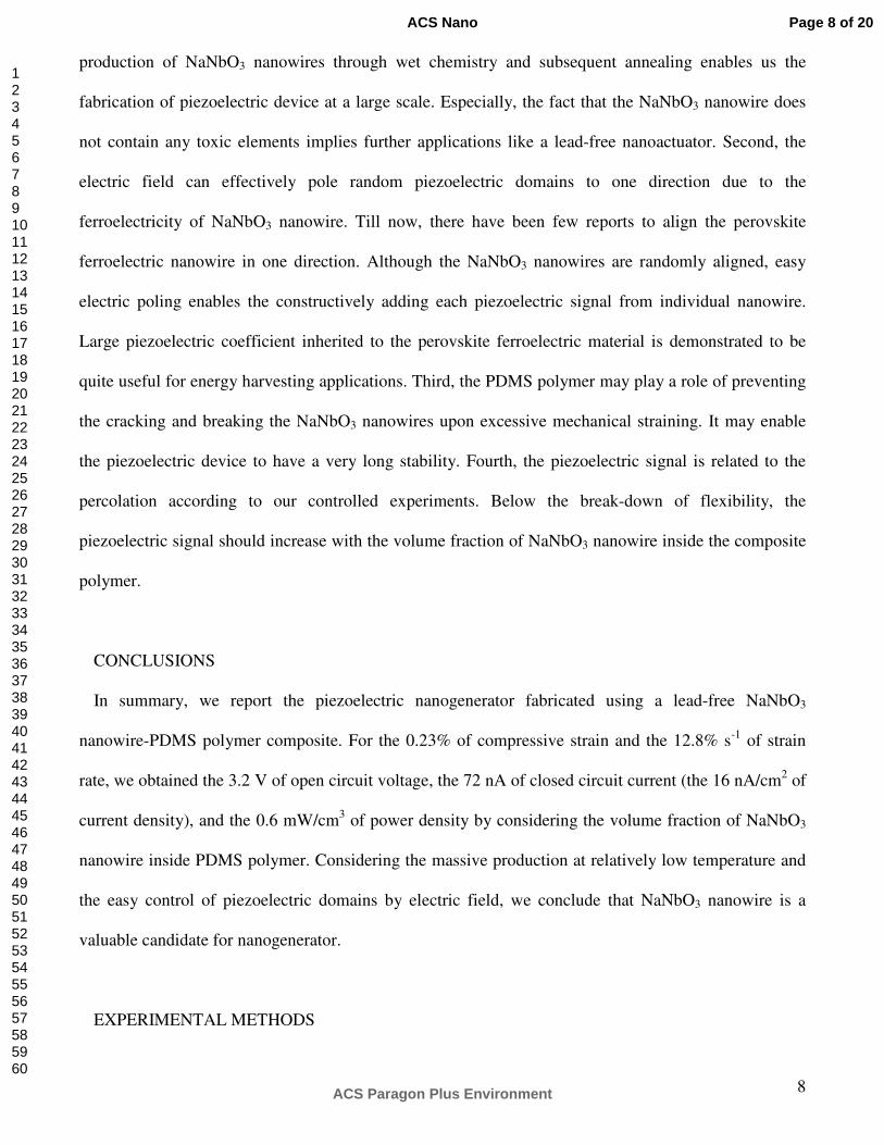
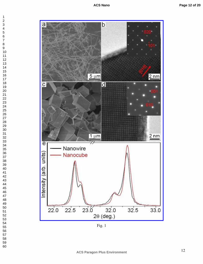
There are two different morphologies of NaNbO3 with nearly the same lattice constant and symmetry
(Figure 1). As described in experimental section, nanowire is formed at short reaction time and
nanocube is at long reaction time by simple hydrothermal method. As grown Na2Nb2O6-H2O nanowires
are successively transformed into NaNbO3 nanowires with the increase of annealing temperature as
confirmed by in-situ x-ray diffraction measurement (supporting information, Figure S1a).15,16 Figure
1a,c show scanning electron microscopy (SEM) images of nanowires and nanocubes, respectively. The
NaNbO3 nanowires have several tens of µm in length and ~200 nm in diameter. On the other hand, the
NaNbO3 nanocubes have 0.5-1.0 µm in lengths. Figure 1b,d show transmission electron microscopy
(TEM) images of a nanowire and a nanocube, respectively. Both nanowire and nanocube show clear
lattice fringes and electron diffraction patterns (insets of Figure 1b,d); suggesting their crystalline
quality. Dark field images show that there are twins along the growth direction for nanowire and in facet
for nanocube (supporting information, Figure S2). X-ray diffraction and electron diffraction give lattice
parameters of a=5.567 Å, b=7.764 Å, c=5.515 Å, and symmetry of P21ma for both annealed nanowires
and as-grown nanocubes (Figure 1e).
Having a P21ma ferroelectric symmetry rather than Pbcm antiferroelectric symmetry in NaNbO3
nanostructures is crucial for NG application, since the former exhibits large piezoelectricity while the
latter does not. Bulk crystalline NaNbO3 has long been indexed as Pbcm symmetry with a=5.506 Å,
b=5.566 Å, c=15.520 Å lattice constants.17 The antiferroelectric Pbcm symmetry is also known to be
changed into ferroelectric P21ma symmetry by applying electric field.18 However, the exceptionally long
c-axis has been questioned by several sophisticate experiments.19-21 Especially, Shiratori et al. reported
that the antiferroelectric Pbcm symmetry in bulk changes into the ferroelectric P21ma symmetry in
submicron sized NaNbO3.22 By accepting the interesting size effect in NaNbO3 nanowires and
nanocubes, we further performed the Rietveld analysis for high-resolution x-ray diffraction pattern
(supporting information, Figure S1b). The obtained x-ray diffraction results can be better fitted by
Page 4 of 20
ACS Paragon Plus Environment
ACS Nano
123456789101112131415161718192021222324252627282930313233343536373839404142434445464748495051525354555657585960
5
P21ma than Pbcm symmetry, as evidenced by smaller fitting error.
Having the ferroelectricity (and inherited piezoelectricity) of NaNbO3 nanowires, we use them for
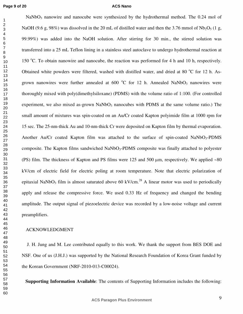
fabricating a NG. Lead-free NaNbO3 nanowires can be obtained at a relatively large quantity. As shown
the photograph of obtained nanowires (Figure 2a), one time reaction in 25-mL-sized vessel can produce
more than 1.2 g of NaNbO3 nanowires without any different morphologies and impurities.
Due to the merit of ferroelectricity (piezoelectricity) and the demerit of random alignment, we formed
a composite of the NaNbO3 nanowire and PDMS polymer in a volume ratio of 1:100 to imbue our NGs
with flexibility. The piezoelectric device mainly consists of four layers as schematically shown in
Figure 2b. The Au/Cr coated Kapton films act as top and bottom electrodes, the NaNbO3 nanowire
mixed with PDMS composite serves as a source of piezoelectric potential, and the thick polyester (PS)
film works as a main driving source of strain. Due to the use of all polymer layers in our NG, the device
could be bent and released for the generation of electricity (inset of Figure 2b). Top view of NaNbO3
nanowire-PDMS polymer composite shows that the nanowires were randomly oriented and well-
dispersed without aggregations (left panel of Figure 2c). For 100×100 µm2 area, we observed 150-200
numbers of nanowires. Cross-section view of the device shows ~100 µm thick NaNbO3-PDMS
composite (right panel of Figure 2c) in which upper and lower layers are Au/Cr coated Kapton films.
Now let us briefly discuss the power generation mechanism. The spontaneous electric dipoles in
NaNbO3, originated from Nb5+ ion movement in NbO6 octahedra, can have six possible orientations
along <001> directions. As shown in Figure 1b, the growth direction of NaNbO3 nanowire is not
parallel to any crystallographic axes. Therefore, the electric dipoles are neither parallel nor
perpendicular to the growth direction of nanowire. Furthermore, the nanowires are randomly oriented
inside the PDMS polymer. When the high electric field is applied, the electric dipoles (black arrows)
would tend to align along the electric field direction (upper panel of Figure 2d). Some ferroelectric
domains (hence piezoelectric domains) will align along the electric field direction, while some domains
may tilt from the electric field direction. However, all of domains have electric dipole components along
Page 5 of 20
ACS Paragon Plus Environment
ACS Nano
123456789101112131415161718192021222324252627282930313233343536373839404142434445464748495051525354555657585960
6
the electric field direction (green arrows). For each NaNbO3 nanowire, we simply considered the same
electric dipole component along the electric field direction. If we apply a compressive force F(t) parallel
to the plane, the NaNbO3 nanowires are under compressive strain (lower panel of Figure 2d). The strain-
induced electric polarization will align to the dipole direction; hence the piezoelectric potential inside
the nanowire is higher at the bottom electrode region than at the top electrode region. In order to screen
the piezoelectric potential, positive and negative charges will be accumulated at the top and bottom
electrodes, respectively. If the compressive strain is released, the piezoelectric potential should be
diminished and the accumulated charges will move back to the opposite direction. Therefore, the
continuously applying and releasing the compressive strain results in the alternating voltage and current,
as similarly discussed in ZnO nanowire based NGs.23,24
The NaNbO3 nanowire-PDMS polymer composite is sandwiched by two Kapton films and a PS
supporting film is placed at the bottom. When we bend the piezoelectric device, a strain neutral line is
located near the PS film. Therefore, the NaNbO3 nanowire-PDMS polymer composite is subject to
compressive strain. From the given Young’s modulus and thickness of each layer, we can calculate the
position of strain neutral line and strain value as shown in supporting information, Figure S3. Since the
thickness of NaNbO3 nanowire-PDMS polymer composite is not thin enough, there should be a
distribution of strain value. To quantitate the value of strain, we determined the strain of composite as
the constant value at the middle of the NaNbO3 nanowire-PDMS polymer composite layer. Since the
Young’s modulus of PDMS (360-870 kPa) is smaller than that of NaNbO3 (80-104 GPa),25,26 the actual
strain of NaNbO3 should be quite small as compared with the strain value of NaNbO3-PDMS composite
listed in the following.
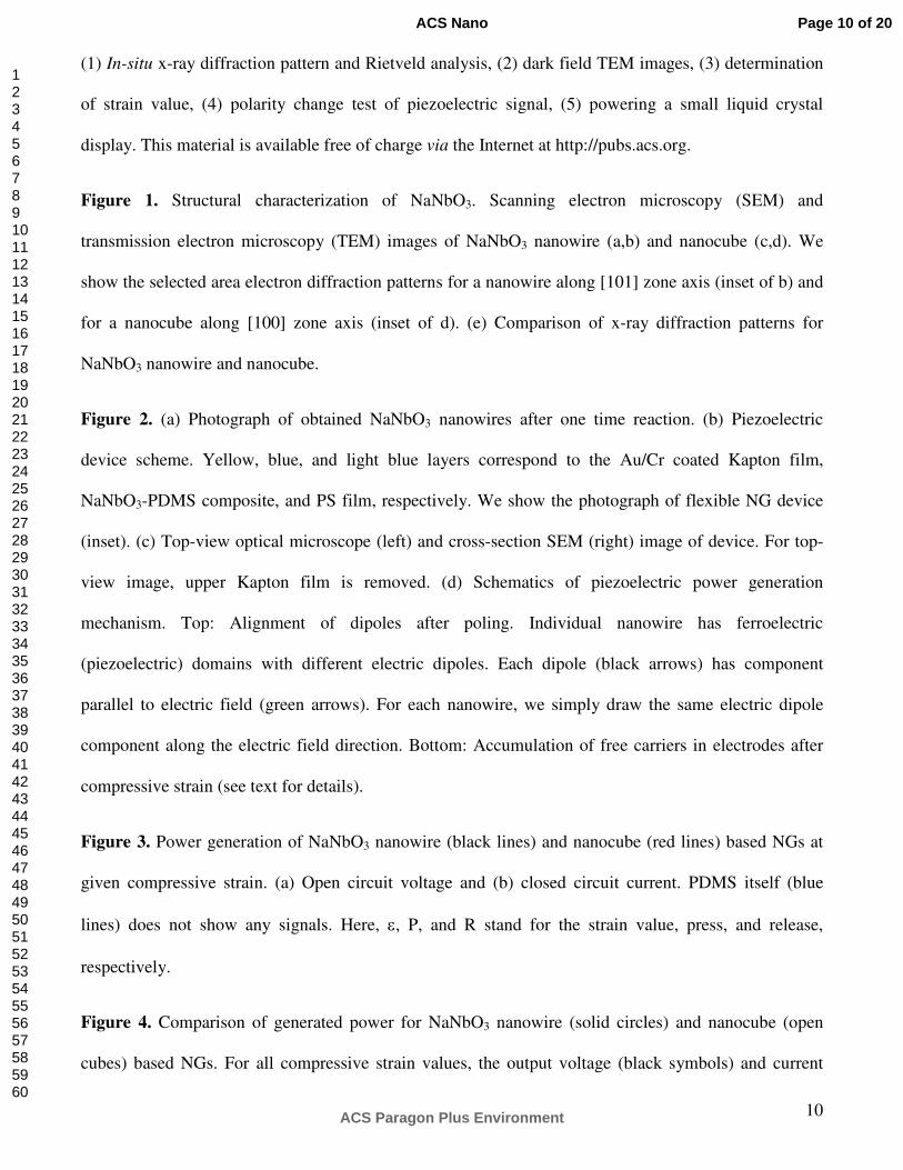
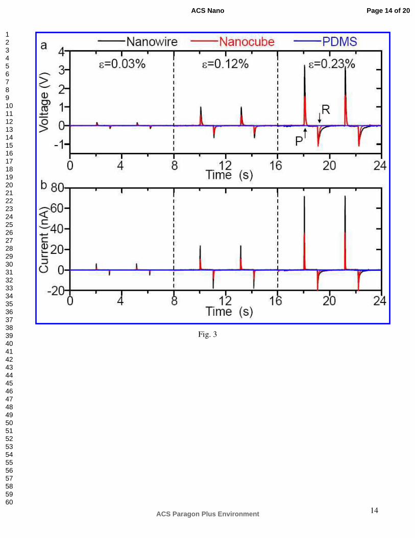
Figure 3a,b show the strain dependences of generated open circuit voltage and closed circuit current,
respectively. To confirm that the obtained signal comes from the piezoelectricity of NaNbO3, we
performed the polarity change test (supporting information, Figure S4).27 In addition, we observed
negligible signals for the device without any electric poling. The generated voltage and current are
Page 6 of 20
ACS Paragon Plus Environment
ACS Nano
123456789101112131415161718192021222324252627282930313233343536373839404142434445464748495051525354555657585960
7
proportional to the applied strain. The different values of voltage and current between press (P) and
release (R) are due to the difference in straining rate when applying and releasing the strain. As clearly
seen, for example, the time interval of generated current for press is almost four times shorter than that
for release. We confirmed that the area in the current-time curve, which related to the total transported
charges, is nearly the same for pressing and releasing. At the strain value of 0.23% and strain rate of
12.8% s-1, the output voltage and current (current density) are estimated to be ~3.2 V and ~72 nA (~16
nA/cm2), respectively, which is enough to power a small liquid crystal display (LCD) (supporting
information, Figure S5). Since NaNbO3 nanowire is mixed with PDMS with a volume ratio of 1:100, we
can assume that the generated power solely from NaNbO3 nanowire is ~0.6 mW/cm3. These values are
higher or comparable to the previous Pb(Zr,Ti)O3 and BaTiO3 based piezoelectric device.10-12
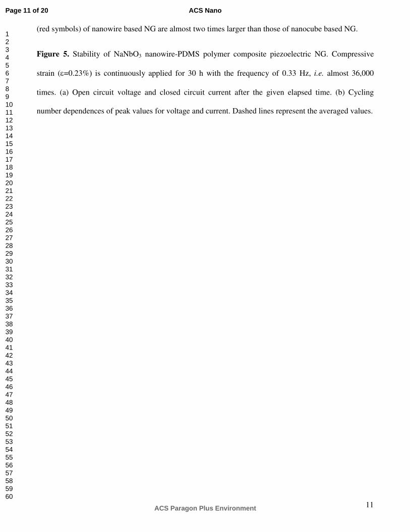
To understand the large output power of NaNbO3 nanowire based NGs, we performed two control
experiments. First, we tested the power generation only from PDMS polymer without NaNbO3
nanowire. The output voltage and current are negligible under the same experimental conditions (strain,
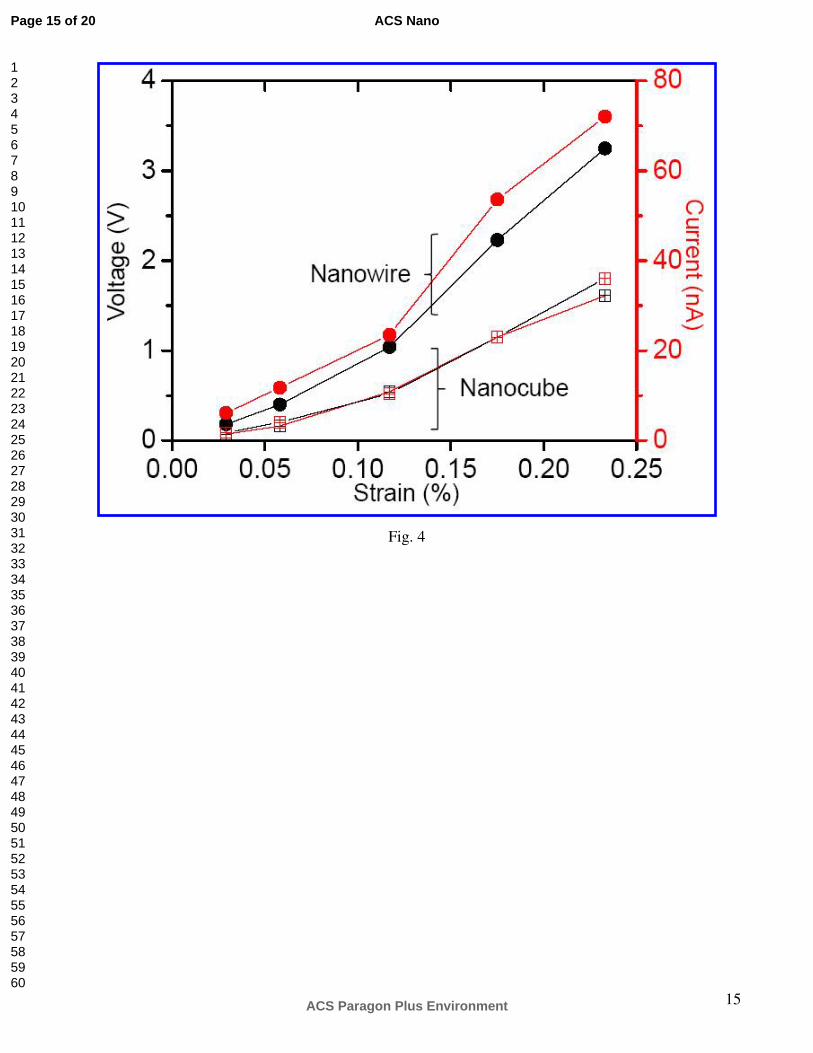
strain rate, and poling voltage). Second, we tested the power generation from NaNbO3 nanocubes based
NG fabricated using the same procedure. Under the same experimental conditions listed above and the
same mixing ratio with PDMS, the output voltage and current from nanocube based NG is almost half
of that from nanowire based NG for all strain values (Figure 4). Since one-dimensional nanowires are
superior to zero-dimensional nanocubes in percolation, a nanowire-based NG could effectively delivers
generated piezoelectric potentials to the outside electrodes compared to a nanocube-based one.
We tested the stability of the NaNbO3 nanowire based piezoelectric NG by continuously applying and
releasing the compressive strain. During almost 30 h, we continuously applied ~36,000 cycles of
straining. While there is some fluctuations, the output voltage and current are very stable (Figure 5a,b).
The mean and standard deviation of output voltage (current) are 3.06 V (70.0 nA) and 0.18 V (3.84 nA),
respectively.
There are several merits for the NaNbO3 nanowire-PDMS composite based NG. First, a massive
Page 7 of 20
ACS Paragon Plus Environment
ACS Nano
123456789101112131415161718192021222324252627282930313233343536373839404142434445464748495051525354555657585960
8
production of NaNbO3 nanowires through wet chemistry and subsequent annealing enables us the
fabrication of piezoelectric device at a large scale. Especially, the fact that the NaNbO3 nanowire does
not contain any toxic elements implies further applications like a lead-free nanoactuator. Second, the
electric field can effectively pole random piezoelectric domains to one direction due to the
ferroelectricity of NaNbO3 nanowire. Till now, there have been few reports to align the perovskite
ferroelectric nanowire in one direction. Although the NaNbO3 nanowires are randomly aligned, easy
electric poling enables the constructively adding each piezoelectric signal from individual nanowire.
Large piezoelectric coefficient inherited to the perovskite ferroelectric material is demonstrated to be
quite useful for energy harvesting applications. Third, the PDMS polymer may play a role of preventing
the cracking and breaking the NaNbO3 nanowires upon excessive mechanical straining. It may enable
the piezoelectric device to have a very long stability. Fourth, the piezoelectric signal is related to the
percolation according to our controlled experiments. Below the break-down of flexibility, the
piezoelectric signal should increase with the volume fraction of NaNbO3 nanowire inside the composite
polymer.
CONCLUSIONS
In summary, we report the piezoelectric nanogenerator fabricated using a lead-free NaNbO3
nanowire-PDMS polymer composite. For the 0.23% of compressive strain and the 12.8% s-1 of strain
rate, we obtained the 3.2 V of open circuit voltage, the 72 nA of closed circuit current (the 16 nA/cm2 of
current density), and the 0.6 mW/cm3 of power density by considering the volume fraction of NaNbO3
nanowire inside PDMS polymer. Considering the massive production at relatively low temperature and
the easy control of piezoelectric domains by electric field, we conclude that NaNbO3 nanowire is a
valuable candidate for nanogenerator.
EXPERIMENTAL METHODS
Page 8 of 20
ACS Paragon Plus Environment
ACS Nano
123456789101112131415161718192021222324252627282930313233343536373839404142434445464748495051525354555657585960
9
NaNbO3 nanowire and nanocube were synthesized by the hydrothermal method. The 0.24 mol of
NaOH (9.6 g, 98%) was dissolved in the 20 mL of distilled water and then the 3.76 mmol of Nb2O5 (1 g,
99.99%) was added into the NaOH solution. After stirring for 30 min., the stirred solution was
transferred into a 25 mL Teflon lining in a stainless steel autoclave to undergo hydrothermal reaction at
150 oC. To obtain nanowire and nanocube, the reaction was performed for 4 h and 10 h, respectively.
Obtained white powders were filtered, washed with distilled water, and dried at 80 oC for 12 h. As-
grown nanowires were further annealed at 600 oC for 12 h. Annealed NaNbO3 nanowires were
thoroughly mixed with poly(dimethylsiloxane) (PDMS) with the volume ratio of 1:100. (For controlled
experiment, we also mixed as-grown NaNbO3 nanocubes with PDMS at the same volume ratio.) The
small amount of mixtures was spin-coated on an Au/Cr coated Kapton polyimide film at 1000 rpm for
15 sec. The 25-nm-thick Au and 10-nm-thick Cr were deposited on Kapton film by thermal evaporation.
Another Au/Cr coated Kapton film was attached to the surface of spin-coated NaNbO3-PDMS
composite. The Kapton films sandwiched NaNbO3-PDMS composite was finally attached to polyester
(PS) film. The thickness of Kapton and PS films were 125 and 500 µm, respectively. We applied ~80
kV/cm of electric field for electric poling at room temperature. Note that electric polarization of
epitaxial NaNbO3 film is almost saturated above 60 kV/cm.28 A linear motor was used to periodically
apply and release the compressive force. We used 0.33 Hz of frequency and changed the bending
amplitude. The output signal of piezoelectric device was recorded by a low-noise voltage and current
preamplifiers.
ACKNOWLEDGMENT
J. H. Jung and M. Lee contributed equally to this work. We thank the support from BES DOE and
NSF. One of us (J.H.J.) was supported by the National Research Foundation of Korea Grant funded by
the Korean Government (NRF-2010-013-C00024).
Supporting Information Available: The contents of Supporting Information includes the following:
Page 9 of 20
ACS Paragon Plus Environment
ACS Nano
123456789101112131415161718192021222324252627282930313233343536373839404142434445464748495051525354555657585960
10
(1) In-situ x-ray diffraction pattern and Rietveld analysis, (2) dark field TEM images, (3) determination
of strain value, (4) polarity change test of piezoelectric signal, (5) powering a small liquid crystal
display. This material is available free of charge via the Internet at http://pubs.acs.org.
Figure 1. Structural characterization of NaNbO3. Scanning electron microscopy (SEM) and
transmission electron microscopy (TEM) images of NaNbO3 nanowire (a,b) and nanocube (c,d). We
show the selected area electron diffraction patterns for a nanowire along [101] zone axis (inset of b) and
for a nanocube along [100] zone axis (inset of d). (e) Comparison of x-ray diffraction patterns for
NaNbO3 nanowire and nanocube.
Figure 2. (a) Photograph of obtained NaNbO3 nanowires after one time reaction. (b) Piezoelectric
device scheme. Yellow, blue, and light blue layers correspond to the Au/Cr coated Kapton film,
NaNbO3-PDMS composite, and PS film, respectively. We show the photograph of flexible NG device
(inset). (c) Top-view optical microscope (left) and cross-section SEM (right) image of device. For top-
view image, upper Kapton film is removed. (d) Schematics of piezoelectric power generation
mechanism. Top: Alignment of dipoles after poling. Individual nanowire has ferroelectric
(piezoelectric) domains with different electric dipoles. Each dipole (black arrows) has component
parallel to electric field (green arrows). For each nanowire, we simply draw the same electric dipole
component along the electric field direction. Bottom: Accumulation of free carriers in electrodes after
compressive strain (see text for details).
Figure 3. Power generation of NaNbO3 nanowire (black lines) and nanocube (red lines) based NGs at
given compressive strain. (a) Open circuit voltage and (b) closed circuit current. PDMS itself (blue
lines) does not show any signals. Here, ε, P, and R stand for the strain value, press, and release,
respectively.
Figure 4. Comparison of generated power for NaNbO3 nanowire (solid circles) and nanocube (open
cubes) based NGs. For all compressive strain values, the output voltage (black symbols) and current
Page 10 of 20
ACS Paragon Plus Environment
ACS Nano
123456789101112131415161718192021222324252627282930313233343536373839404142434445464748495051525354555657585960
11
(red symbols) of nanowire based NG are almost two times larger than those of nanocube based NG.
Figure 5. Stability of NaNbO3 nanowire-PDMS polymer composite piezoelectric NG. Compressive
strain (ε=0.23%) is continuously applied for 30 h with the frequency of 0.33 Hz, i.e. almost 36,000
times. (a) Open circuit voltage and closed circuit current after the given elapsed time. (b) Cycling
number dependences of peak values for voltage and current. Dashed lines represent the averaged values.
Page 11 of 20
ACS Paragon Plus Environment
ACS Nano
123456789101112131415161718192021222324252627282930313233343536373839404142434445464748495051525354555657585960
12
Fig. 1
Page 12 of 20
ACS Paragon Plus Environment
ACS Nano
123456789101112131415161718192021222324252627282930313233343536373839404142434445464748495051525354555657585960

13
Fig. 2
Page 13 of 20
ACS Paragon Plus Environment
ACS Nano
123456789101112131415161718192021222324252627282930313233343536373839404142434445464748495051525354555657585960
14
Fig. 3
Page 14 of 20
ACS Paragon Plus Environment
ACS Nano
123456789101112131415161718192021222324252627282930313233343536373839404142434445464748495051525354555657585960
15
Fig. 4
Page 15 of 20
ACS Paragon Plus Environment
ACS Nano
123456789101112131415161718192021222324252627282930313233343536373839404142434445464748495051525354555657585960

16
Fig. 5
Page 16 of 20
ACS Paragon Plus Environment
ACS Nano
123456789101112131415161718192021222324252627282930313233343536373839404142434445464748495051525354555657585960
17
REFERENCES AND NOTES
1. Dresselhaus, M. S.; Thomas, I. L. Alternative Energy Technologies. Nature 2001, 414, 332-337.
2. Wang, Z. L. Self Powered Nanotech. Sci. Am. 2008, 298, 82-87.
3. Wang, Z. L.; Song, J. H. Piezoelectric Nanogenerators Based on Zinc Oxide Nanowire Arrays.
Science 2006, 312, 242–246.
4. Wang, X. D.; Song, J. H.; Wang, Z. L. Direct-Current Nanogenerator Driven by Ultrasonic Waves.
Science 2007, 316, 102-105.
5. Qin, Y.; Wang, X. D.; Wang, Z. L. Microfibre–Nanowire Hybrid Structure for Energy Scavenging.
Nature 2008, 451, 809-813.
6. Choi, D.; Choi, M.-Y.; Choi, W. M.; Shin, H.-J.; Park, H. K.; Seo, J.-S.; Park, J.; Yoon, S. M.; Chae,
S. J.; Lee, Y. H.; et al. Fully Rollable Transparent Nanogenerators Based on Graphene Electrodes. Adv.
Mater. 2010, 22, 2187-2192.
7. Suyal, G.; Colla, E.; Gysel, R.; Cantoni, M.; Setter, N. Piezoelectric Response and Polarization
Switching in Small Anisotropic Perovskite Particles. Nano Lett. 2004, 4, 1339-1342.
8. Yun, W. S.; Urban, J. J.; Gu, Q.; Park, H. Ferroelectric Properties of Individual Barium Titanate
Nanowires Investigated by Scanned Probe Microscopy. Nano Lett. 2002, 2, 447-450.
9. Rørvik, P. M.; Grande, T.; Einarsrud, M.-A. One-Dimensional Nanostructures of Ferroelectric
Perovskites. Adv. Mater. 2011, 23, 4007-4034.
10. Chen, X.; Xu, S.; Yao, N.; Shi, Y. 1.6 V Nanogenerator for Mechanical Energy Harvesting Using
PZT Nanofibers. Nano Lett. 2010, 10, 2133–2137.
Page 17 of 20
ACS Paragon Plus Environment
ACS Nano
123456789101112131415161718192021222324252627282930313233343536373839404142434445464748495051525354555657585960

18
11. Xu, S.; Hansen, B. J.; Wang, Z. L. Piezoelectric-Nanowire-Enabled Power Source for Driving
Wireless Microelectronics. Nature Comms.2010, 1, 93.
12. Park, K-I.; Xu, S.; Liu, Y.; Hwang, G. T.; Kang, S. J. L.; Wang, Z. L.; Lee, K. J. Piezoelectric
BaTiO3 Thin Film Nanogenerator on Plastic Substrates. Nano Lett. 2010, 10, 4939–4943.
13. Cross, L. E. Materials Science: Lead-Free at Last. Nature 2004, 432, 24-25.
14. Saito, Y.; Takao, H.; Tani, T.; Nonoyama, T.; Takatori, K.; Homma, T.; Nagaya, T.; Nakamura, M.
Lead-Free Piezoceramics. Nature 2004, 432, 84-87.
15. Zhu, H. Y.; Zheng, Z. F.; Gao, X. P.; Huang, Y. N.; Yan, Z. M.; Zou, J.; Yin, H. M.; Zou, Q. D.;
Kable, S. H.; Zhao, J. C.; et al. Structural Evolution in a Hydrothermal Reaction between Nb2O5 and
NaOH Solution: From Nb2O5 Grains to Microporous Na2Nb2O6-2/3H2O Fibers and NaNbO3 Cubes. J.
Am. Chem. Soc. 2006, 128, 2373-2384.
16. Liu, L.; Li, B.; Yu, D.; Cui, Y.; Zhou, X.; Ding, W. Temperature-Induced Solid-Phase Oriented
Rearrangement Route to the Fabrication of NaNbO3 Nanowires. Chem. Commun. 2010, 46, 427-429.
17. Sakowski-Cowley, A. C.; Lukaszewicz, K.; Megaw, H. D. The Structure of Sodium Niobate at
Room Temperature, and the Problem of Reliability in Pseudosymmetric Structures. Acta Crystallogr.
1969, B25, 851-865.
18. Ulinzheev, A. V.; Leiderman, A. V.; Smotrakov, V. G.; Topolov, V. Yu.; Fesenko, O. E. Phase
Transitions Induced in NaNbO3 Crystals by Varying the Direction of an External Electric Field. Phys.
Solid State 1997, 39, 972-974.
19. Johnston, K. E.; Tang, C. C.; Parker, J. E.; Knight, K. S.; Lightfoot, P.; Ashbrook, S. E. The Polar
Phase of NaNbO3: A Combined Study by Powder Diffraction, Solid-State NMR, and First-Principles
Calculations. J. Am. Chem. Soc. 2010, 132, 8732-8746.
Page 18 of 20
ACS Paragon Plus Environment
ACS Nano
123456789101112131415161718192021222324252627282930313233343536373839404142434445464748495051525354555657585960
19
20. Yan, C.; Nikolova, L.; Dadvand, A.; Harnagea, C.; Sarkissian, A.; Perepichka, D. F.; Xue, D.;
Rosei F. Multiple NaNbO3/Nb2O5 Heterostructure Nanotubes: A New Class of
Ferroelectric/Semiconductor Nanomaterials. Adv. Mater. 2010, 22, 1741–1745.
21. Yuzyuk, Yu. I.; Shakhovoy, R. A.; Raevskaya, S. I.; Raevski, I. P.; Marssi, M. E.; Karkut, M. G.;
Simon, P. Ferroelectric Q-Phase in a NaNbO3 Epitaxial Thin Film. Appl. Phys. Lett. 2010, 96, 222904.
22. Shiratori, Y.; Magrez, A.; Dornseiffer, J.; Haegel, F.-H.; Pithan, C.; Waser, R. Polymorphism in
Micro-, Submicro-, and Nanocrystalline NaNbO3. J. Phys. Chem. B 2005, 109, 20122-20130.
23. Zhang, Y.; Liu, Y.; Wang, Z. L. Fundamental Theory of Piezotronics. Adv. Mater. 2011, 23,
3004-3013.
24. Hu, Y. F.; Zhang, Y.; Xu, C.; Zhu, G.; Wang, Z. L. High-Output Nanogenerator by Rational
Unipolar Assembly of Conical Nanowires and Its Application for Driving a Small Liquid Crystal
Display. Nano Lett. 2010, 10, 5025-5031.
25. Egerton, L.; Dillon, D. M. Piezoelectric and Dielectric Properties of Ceramics in the System
Potassium-Sodium Niobate. J. Am. Ceram. Soc. 1959, 42, 438-442.
26. Palatnikov, M. N.; Shcherbina, O. B.; Efremov, V. V.; Sidorov, N. V.; Salak, A. N. Microstructure
and Elastic Modulus of Ceramic LixNa1 – xNbO3 Perovskite Solid Solutions Prepared at 6 GPa. Inorg.
Mater. 2010, 46, 1348-1352.
27. Yang, R.; Qin, Y.; Dai, L.; Wang, Z. L. Power Generation with Laterally-Packaged Piezoelectric
Fine Wires. Nat. Nanotech. 2009, 4, 34-39.
28. Mino, T.; Kuwajima, S.; Suzuki, T.; Kanno, I.; Kotera, H.; Wasa, K. Piezoelectric Properties of
Epitaxial NaNbO3 Thin Films Deposited on (001)SrRuO3/Pt/MgO Substrates. Jpn. J. Appl. Phys. 2007,
46, 6960-6963.
Page 19 of 20
ACS Paragon Plus Environment
ACS Nano
123456789101112131415161718192021222324252627282930313233343536373839404142434445464748495051525354555657585960

20
TOC
We present a piezoelectric nanogenerator device fabricated using a lead-free NaNbO3 nanowire and
poly(dimethylsiloxane) (PDMS) polymer composite. Under the compressive strain of 0.23%, the device
shows high output voltage of 3.2 V and current of 72 nA. Due to the merits of the massive production at
relatively low temperature and the easy control of piezoelectric domains by electric field, NaNbO3
nanowire should be quite useful for the large-scale high output piezoelectric nanogenerator applications.
Page 20 of 20
ACS Paragon Plus Environment
ACS Nano
123456789101112131415161718192021222324252627282930313233343536373839404142434445464748495051525354555657585960


![Bending piezoelectric nanowires: application to force ...€¦ · [6] D. Lincot, “Solution growth of functional zinc oxide films and nanostructures,” MRS Bull., vol. 35, no. October,](https://img.pdfslide.us/doc/110x75/5ea804eb2022bf2e5242886b/bending-piezoelectric-nanowires-application-to-force-6-d-lincot-aoesolution.jpg)