Embed Size (px)
Citation preview
Label-free sensing with semiconducting nanowires
A Dissertation Presented to the Faculty of the Graduate School
of Yale University
in Candidacy for the Degree of Doctor of Philosophy
by Eric Stern
Dissertation Director: Prof. Mark A. Reed
May 2007
1
Abstract
Label-free sensing with semiconducting nanowires
Eric Stern
2007
Nanoscale electronic devices have the potential to achieve exquisite sensitivity as sensors
for the direct detection of molecular interactions, thereby decreasing diagnostics costs
and enabling previously impossible sensing in disparate field environments.
Semiconducting nanowire-field effect transistors (NW-FETs) hold particular promise,
though contemporary NW approaches are inadequate for realistic applications. We
present here a novel approach using complementary metal-oxide-semiconductor (CMOS)
technology that has not only achieved unprecedented sensitivity, but simultaneously
facilitates system-scale integration of nanosensors for the first time. This approach
enables a wide range of label-free biochemical and macromolecule sensing applications,
including cell type discrimination through the monitoring of live, stimulus-induced
cellular response, and specific protein and complementary DNA recognition assays. An
important achievement is the introduction of real-time, unlabeled detection capability,
allowing for fundamental studies of cellular activation, and specific macromolecule
interactions at concentrations (<femtomolar) orders of magnitude lower than other
commonly available techniques.
2

© 2007 by Eric Stern All Rights Reserved.
3

To Alan Stern, who taught me more about life, family, hard work—and in turn myself—over the
past four years than I ever thought I’d know
4

Acknowledgements
There are more people than I can count who helped make this work possible. I owe a
huge debt of gratitude to my advisor, collaborators, and coworkers, as well as to my
family and friends (those categories are not mutually exclusive). And, of course, I am
indebted to the agencies sponsoring the graduate fellowships I was fortunate enough to be
awarded, the Department of Homeland Security and the National Science Foundation.
First and foremost I thank Prof. Mark Reed, my boss, for keeping me in his laboratory at
Yale for another four years and for being not only merely a truly exceptional mentor (and
bill-payer) but also a good, trusted friend. My last four years have been one of the most
spectacular periods of my life due primarily to the countless hours I spent in the Becton
Center under his tutelage. I have had a truly unbelievable experience working in his
laboratory and plan to maintain a close collaboration, at the very least, for a long time to
come.
I also thank all my committee members for their exceptional support for my work and for
their advice and friendship. From the outset of my project, Prof. Fred Sigworth raised a
number of critical concerns. Without accounting for his crucial observations, which
required countless conversations throughout the course of the work, the project quite
simply would not have worked. Also from the outset of my graduate career, I was
fortunate enough to have a second laboratory, Prof. David LaVan’s, opened to me. The
chemical reactions and surface characterizations I performed in this second home, as well
5
as the conversations I had with Prof. LaVan, were critical at every step of my project.
Although my interactions with Prof. Tarek Fahmy began later in the course of my work,
this collaboration has proven to be the most fruitful of my life. Seemingly not a single
experiment has been performed by me in the last year (many, incidentally, in his
laboratory) without thorough discussions (generally after midnight) with Prof. Fahmy and
I look forward to many more such conversations in the future as a postdoctoral researcher
in his lab.
Many of the current and former Reed group members have not only helped incredibly
with my work but shaped me as a scientist as well. Professors Ilona Kretzschmar (City
College of New York) and Guosheng Cheng (Suzhou University) were not only
instrumental in teaching me to perform engineering research but also taught me the value
of collaboration. Without them, much of the work presented here could not have even
been started. James Klemic helped me through my work every step along the way not
only scientifically but also has a good friend. Professor Takhee Lee (Gwangju Institute
of Science and Technology) and Doctors Menno de Jong and Glenn Martin, though
present for only a brief period during my thesis work, taught me an incredible amount
about research and the required work ethic. Aleksandar Vacic, though only present at the
tail end of the work, was instrumental for the theoretical studies and I leave knowing the
nanobars are in great hands with him and David Routenberg, who helped me through
many of the rough spots and performed some of the most exciting and important device
physics experiments. Additionally, Dr. Marleen van der Veen’s infectious personality
and work ethic helped reinvigorate me during the last months of the work and she should
6

join Alek and David as a member of a very high-flying Reed group team in the future.
Doctors Jia Chen and Jeff Sleight, though graduated before I showed up, provided
exceptional help with many experiments. Additionally, Doctors Elena Cimpoiasu, Nilay
Pradhan, Wenyong Wang, Xiaohui Li, and Jie Su, in addition to Stan Guthrie, Ryan
Munden, and Aric Sanders contributed to sample growth and device measurements.
Matthew Phillips, though only present transiently, provided strong encouragement.
I have been blessed with having some truly exceptional undergraduates working for me
over time who have greatly contributed to the results. Daniel Turner-Evans began just as
the work got exciting and his fingerprints are all over the work presented here. Robin
Wagner single-handedly laid the groundwork not only for my final experiments but for
much of the future work I hope to accomplish. Carl Dietz and Eric Steinlauf, though in
lab just a bit too early to catch the most exciting work, contributed greatly to my original
understanding of the sensors. Burt Helm, Elizabeth Broomfield, Shin Rong Lee, Jamie
Capo, and Maria (Gaby) Oronchea (not under my direct supervision) also performed
some interesting and critical experiments.
As a very fortunate pseudo-member of the Fahmy group for the final semesters of my
work, I have had the opportunity to work with his exceptional students and very much
look forward to continuing these relationships. Erin Steenblock provided samples, a
watchful eye, and good luck for some of my final experiments and traveled more miles
with me than any other collaborator. Jason Park, Stacey Demento, Jason Criscione, and
Tarek Fadel have provided great encouragement and much of the work we have recently
7
collaborated on will come to spectacular fruition under their direction. And the members
of the Fahmy group undergraduate army, Michaela Panter, Karlo Perica, Karen Chen,
Katie Allen, Gilbert Addo, Atu Agawu, Jeffrey Reitman, and Sean Mehra, have also
contributed not only to the work but to making it fun.
There are many professors in addition to my committee members whose advice and
support was instrumental and who have helped make my Yale graduate experience
exceptional. Yale Professors T. P. Ma, Jung Han, Jerry Woodall, Peter Kindlmann,
Yiorgos Makris, Eugenio Culurciello, Hur Koser, and Robert Schoelkopf helped at many
steps with device design and fabrication. Yale Professors Mark Saltzman, Michael
Levene, Ron Breaker, Michael Snyder, Andrew Hamilton, Eric Dufresne, John Wood,
Glenn Micalizio, Erin Lavik, and Dennis Spencer helped throughout my work with
functionalization and sensing. I also enjoyed very fruitful collaborations with Professors
Tadeusz Malinski of Ohio University and Chonwu Zhou of the University of Southern
California, and Dr. Jack Yu of the Medical College of Georgia. Professors Jonathan
Schneck (Johns Hopkins University), Herman Eisen (Massachusetts Institute of
Technology), and Ruslan Medzhitov provided critical samples for cellular response
measurements. Additionally, I am indebted to Profs. James Duncan, Fahmeed Hyder,
Saltzman, and Fahmy for selecting me as a Teaching Assistant for their classes and to
Prof. Levene for allowing me to be a guest lecturer in the Senior Seminar.
There are countless Yale researchers in addition to my group memebers whose advise,
assistance, and support was essential to my progress. I will try to name them all, but so
8
many people have been helpful throughout time that I apologize in advance if I forget
some. In my eyes Thomas Boone and Robert Koudelka were always the ideal graduate
students and have always been a great example for me and both workers and friends.
Pauline Wyrembak single-handedly made functionalization possible by providing every
molecule I needed. James Hyland helped minimize the drudgery of the Yale cleanroom
and seemingly provided key suggestions every day and Christopher Tillinghast and
Michael Young allowed that advice to be useful by keeping the cleanroom up and
running (and also gave many critical suggestions themselves). Doctor Kathryn Klemic in
addition to James Bertram, Steven Jay, Benjamin Boese, and Alexis de Kerchove assisted
with (and oftentimes did) crucial studies that made some papers possible. Doctors Luigi
Frunzio, Jun-Fei Zheng, Hironori Tsukamoto, George Cui, Zhenting Jiang, and Sharon
Cui and Matthew Reese and David Schuster gave me many processing and metrology
tips throughout the course of the work. Tania Henry, Manisha Gupta, Sara Hashmi,
Joseph McManis, Yanxiang Liu, Weipeng Li, Chun-Chen Yeh, Joseph Schreier, Tolga
Kaya, Dechao Guo, Bozidar Marinkovic, Ayse Kose, Jason Hoffman, Liyang Song,
Miaomiao Wang, Chad Rigetti, Veronica Savu, Ning Li, and Sun Il Shim all look great in
bunny suits and helped make working in the cleanroom almost fun. I also had many
fruitful discussions that helped both the work succeed and time pass with Drs. Peter
Fong, Jeremy Blum, and Hung Te Hsieh in addition to Millicent Ford, Jeffrey
McCutcheon, Sara Royce-Hynes, Andrew Sawyer, Jennifer Saucier-Sawyer, Thomas
Chia, Andrew Barthel, Richard Torres, Zai Yuan Ren, and Qian Sun.
9
Many researchers and companies outside Yale played significant roles in my project.
Robert Ilic, Daron Westly, Meredith Metzler, and Vincent Genova of the CNF taught me
real processing and their help and suggestions made the sensor fabrication possible.
Doctor Ling Xie and John Tsakirgis of the Harvard Cleanroom provided much-needed
fabrication assistance when the Yale Cleanroom was down. Doctors Emanuel Tutuc and
Robert Klie made and measured samples, respectively, that added incredible dimensions
to my work. Alec Flyer made some of the most critical functionalization suggestions that
enabled the work to continue. Additionally, a number of companies routinely went well
out of their way to help me meet my deadlines: CAD Art Servies, Benchmark
Technologies, nTEK, and Innovion.
The support of Yale’s staff also made the projects possible. Many of the apparatuses on
or in which experiments were run were built by Vincent, Nick, or Russel Bernardo. No
progress towards academic completion would ever occur without Cara Gibilisco and no
reagents or supplies would ever show up without the dedication of Vivian Smart, Arlene
Ciociola, Patricia Kakalow, Deanna Lomax, Elna Godburn, Senen Antunez and Susan
Johns. And the company of the Becton custodial staff at all times of the day and night
always helped to keep me going.
Additionally, I owe a huge debt of gratitude to Dean Paul Fleury, Claudia Merson, and
Bridget Calendo for making the Yale Engineering Futures in Science Research
Fellowship (YEFSRF) a reality and to them and Prof. Levene, Dr. Joanna Price, and
Steven Jay for continuing it. And I am very thankful to the students in my classes for
10

supporting me as a TA while I learned the ropes and for (mostly) doing great work that
made my life incredibly easy.
And since altruism isn’t always the name of the game, I owe a huge debt of gratitude to
all the Yale Office of Cooperative Research employees, especially James Boyle.
Without the constant support of my family and friends I never could have dealt with the
(constant) setbacks and the eventual success would mean nothing. Words truly can’t
express how lucky I feel to have had them there every step along the way. My Mom and
Dad started me in this game and, man, do I love it—and what other parents would also
serve as the final evaluator of all papers? The constant love and support of (and interest
in my work) my Grandma and Grandpa, my Uncle Don and Aunt Antje, and my cousins
Bobby and Elizabeth, mean more than I can ever express. My brother, Alan, is the best
brother a guy could ever ask for and my best friend and I can’t wait to get to Boston in
good part because he’s there. My fill-in-something-here, Laura, was there every step
along the way and made me who I am today as both a person and a scientist—nearly
every piece of data here was taken with her on the phone or in my office and most
definitely in my heart; the last datafiles, named “tnxljg__” say it all. And the friendship
and support her parents, Mr. and Mrs. Greer, both means and has taught me more than I
can explain. My best friends James, Steve, Mike, Rob, Park, Pauline, and Jen D, kept me
going day-in and day-out and made grad school one of the best experiences of my life
outside the lab as well as in it. And the friendship and support of Rachael and Sarah Mc,
along with Jeremiah, Cutch, BD, Zak, Vip, Cogs, Fong, Tarek, Tom C, Andy, Rick,
11

Marc, Raul, Jan, Andy S, Dwayne, Chu, Rasika, Tom B, Rob K, Jimmy, Diego, Bill,
Ashley, Elnaz, Tara, Carey, Julie, Sara, Rachel, Lauren H, Amy, Jen G, Jenny, Giggles,
Vomit, Chillable, Stace, Erin, Vivian, Rutkow, Flyer, Cole, Moral, Dan, Jesse, Goldy,
Lusty, the rest of the jellydonut crowd, and everyone else has made time fly. Thank you!
And I also thank Gourmet Heaven for serving a spectacular sandwich just about every
other night for the past two-and-a-half years, GPSCY and Thai Taste for Thursday nights,
and Anna Liffey’s and Solo cups for Fridays.
12
Contents
List of Tables …………………………………………………………………….. 15 List of Figures ……………………………………………………………………. 16 1 Introduction ……………………………………………………………… 18 References …………………………………….……..……………. 27 2 Theoretical Considerations …………………………………………….... 39 2.1 Importance of Device Scaling on Sensitivity ...……........................ 39 2.2 pH Response …………………………...……………..…………… 41 2.3 Functionalization and Molecular Binding Considerations ……..…. 44 2.4 Chamber Design and Solution Exchange Considerations ………… 49 2.5 Debye Screening Considerations ………………………………….. 54 2.6 Conclusions ………………………………………………………... 56 References …………………………………….……..……………. 57 3 Nanobar Fabrication and Characterization …...……………………….. 61 3.1 Nanobar Fabrication ……..………………………………………... 61 3.2 Nanobar Characterization …………………………………………. 68 3.3 Conclusions ……………………………………………………….. 72 References …………………………………….……..……………. 74 4 Functionalization Techniques for Protein and DNA Conjugation ….... 79 4.1 Introduction ……………………………………………………….. 79 4.2 Oxidative Electropolymerization-Based Functionalization ………. 80 4.3 Electrically-Directed Silicon Functionalization …………………... 86 4.4 Silicon-Specific, Non-Electrically Directed Functionalization …… 88 4.5 Non-Silicon-Specific, Non-Electrically Directed Functionalization 91 4.6 Conclusions ……………………………………………………….. 92 References …………………………………….……..……………. 93
13
5 Nanobar Sensing ……………………………………….………………… 99 5.1 Introduction ……………………………………………………….. 99 5.2 Unfunctionalized NB Sensing …………………………………….. 100 5.3 Unfunctionalized NB Sensing of Specific Cellular Responses …… 105 5.4 Silicon-Specific NB Functionalization ……………………………. 112
5.5 Nanobar Sensor Characterization …………………………………. 116 5.6 Nanobar Sensing of Unlabeled Proteins and DNA ………………... 125 5.7 Conclusions ……………………………………………………….. 130 References …………………………………….……..……………. 131 6 Conclusions ………………………………………………………………. 139 References …………………………………….……..……………. 142 Appendix I: Functionalization Methods ………………………………………... 144 Appendix II: Sensing Methods ………………………………………………….. 168 Appendix III: Nanowire-Field Effect Transistors ……...……………………… 181
14

List of Tables Table 2.1 …………………... 56 Table 4.1 …………………... 90
15

List of Figures Figure 2.1 …………………. 40 Figure 4.9 ..………………... 90 Figure 2.2 …………………. 46 Figure 4.10 ………………... 92 Figure 2.3 …………………. 50 Figure 5.1 ..………………... 101 Figure 2.4 …………………. 52 Figure 5.2 ..………………... 103 Figure 2.5 …………………. 53 Figure 5.3 ..………………... 104 Figure 3.1 …………………. 63 Figure 5.4 ..………………... 107 Figure 3.2 …………………. 65 Figure 5.5 ..………………... 108 Figure 3.3 …………………. 66 Figure 5.6 ..………………... 110 Figure 3.4 …………………. 67 Figure 5.7 ..………………... 112 Figure 3.5 …………………. 68 Figure 5.8 ..………………... 113 Figure 3.6 …………………. 70 Figure 5.9 ..………………... 114 Figure 3.7 …………………. 71 Figure 5.10 ………………... 115 Figure 3.8 …………………. 72 Figure 5.11 ………………... 116 Figure 4.1 …………………. 81 Figure 5.12 ………………... 117 Figure 4.2 …………………. 82 Figure 5.13 ………………... 118 Figure 4.3 …………………. 83 Figure 5.14 ………………... 119 Figure 4.4 …………………. 84 Figure 5.15 ………………... 120 Figure 4.5 …………………. 85 Figure 5.16 ………………... 122 Figure 4.6 …………………. 87 Figure 5.17 ………………... 123 Figure 4.7 …………………. 88 Figure 5.18 ………………... 124 Figure 4.8 …………………. 89 Figure 5.19 ………………... 126
16

Figure 5.20 ..………………. 126 Figure 5.22 .……………….. 128 Figure 5.21 ..………………. 127 Figure 5.23 .……………….. 129
17
Chapter 1: Introduction
The importance of sensing chemicals and biochemicals in disparate field environments
cannot be underestimated in today’s world [1-13]. Sensing small numbers of molecules
exactly, effectively, and expeditiously is paramount for army defense and homeland
security [1-3], clinical screening and diagnoses [4-8], drug discovery [9,10], and basic
research assays [7,8,10,11]. For each of these applications, it is highly desirable that an
ultrasensitive, small, versatile, robust, low-power, easy-to-use, inexpensive, variable-
sensitivity sensor be created [1,4,11-13]. In spite of the critical demand for such a sensor,
no single technology has yet shown the capability to meet all of these requirements [11-
29].
Sensors can be roughly grouped into two major categories: those that identify molecules
spectroscopically [30-35], or those that use a direct or indirect means of sensing a
specific molecule [36-47]. The detection of small molecules is readily achieved with
sensors in the first category and, due to the success of such technologies, many are now
being scaled down. In spectroscopic approaches, the aforementioned desirable
requirements have stimulated the development of miniaturized gas chromatographs [32],
Fourier transform infrared spectrometers [33], mass spectrometers [32,34], and solid-state
gas-phase sensors [37,40,41]. However, many of these techniques face lower limits on
size due to scaling limitations and lower limits on power dissipation because of the
fundamental physical phenomena by which they operate [12]. Furthermore, these
18
methods are generally incapable of sensing large molecular species, such as proteins and
viruses [11-16].
In contrast, the macromolecular sensing required for biological research and clinical
applications is predominantly achieved by specific-molecule detection methods [39-44]
because these molecules are often too complex for spectroscopic recognition [11-16].
Specific-molecule detection techniques can be further divided into those solely reliant
upon chemical means for detection [43,44], and those that convert the chemical signal
into an electrical one [39-42]. Methods in the former category—such as enzyme-linked
immunosorbent [43] and immunoblotting [44] assays, or fluorescence/radioisotope/dye
labeling [45]—are significantly more sensitive but are of marginal utility outside the
laboratory environment (with some exceptions, such as home pregnancy tests) [11-16].
As sensing in disparate field environments becomes increasingly critical, development
has begun on a number of label-free, specific-molecule technologies for converting
chemical signals to electrical ones without the need for complex sample preparation [17-
29]. The most established approaches are metallic potentiometric [46] and amperometric
[24] sensors, which sense ions electrochemically in solution; solid state [37,47]
conductance sensors, which sense gas-phase ions and small molecules by measuring the
absorption-induced conductance change of a material; and chemical field effect
transistors (chemFETs; a type of ion sensitive field effect transistor, ISFET), which sense
ions in solution by charge modification of the gate of a FET [42,48]. Though each of
these techniques has been successful for various applications—metallic potentiometric
19
and amperometric sensors for small molecules and ions [48,49], solid-state gas sensors
for chlorine and fluorine [37], and chemFETs for glucose and other small molecules
[48,50,51]—none are very sensitive (detection limits are generally parts per million).
One method that has successfully overcome this sensitivity barrier and currently serves as
the standard for unlabeled sensing is surface plasmon resonance [52]. In this approach,
an antibody of the protein to be sensed is attached to a thin gold film. The angular
reflection of a laser beam off the backside of the gold is dependent on the local dielectric
constant; binding of the protein changes the dielectric constant, and thus deflects the laser
beam. However this technique has not met with success outside research environments
due to its price, size, high-power, and mechanical alignment issues.
The lack of a scalable, inexpensive, label-free sensing technology has resulted in a
number of new methods that are currently under development. A few of note are
cantilever-sensors, which sense the binding of a desired molecule to a thin catilever by
measuring the deflection of the beam with a laser or piezoresistive elements [19,53];
fiber-optic sensors, which sense the binding of nanoparticle-linked antibodies to a protein
after that protein binds a specific antibody conjugated to a fiber-optic strand [23];
waveguide sensors, which sense the presence of a specifically bound protein to an
antibody film on a chip between two waveguides [21,22]; and nanoparticle-solution
sensors, in which the binding of a specific protein to an antibody-coated nanoparticle
results in the attachment of a second nanoparticle, resulting in a color change [20,54,55].
Though each of these methods has shown promise, none simultaneously meets the
20
requirements in terms of sensitivity, versatility, and power consumption. Only the
cantilevers enable label-free sensing, a key requirement for many applications [1,3-13].
Due to these shortcomings, researchers have returned to the solid state condutance
sensors and chemFETs and sought to increase their sensitivity and versatility by reducing
the lateral dimensions of the devices in order to maximize the effect of surface charge on
device transport. When modified indium oxide (In2O3) FET sensors are scaled down to a
quasi-one-dimensional single-crystal nanowire (NW) [59,60], the resulting device can
achieve a NO2 sensitivity of ~1 ppb [61,62] as compared to ~1 ppm for larger devices
[56-58] , a three-order-of-magnitude increase in sensitivity. The cause of this sensitivity
increase is the maximized surface area-to-volume ratio of the NW-FET: the geometry of
the NW restricts current flow to a much thinner region than in the bulk, and thus
adsorbed molecules on the surface exert more significant effects [63-65]. Though
multiple successful demonstrations have been performed with NWs [66-70], carbon
nanotubes (CNTs) [71,72], and electrospun nanofibers [73], the drawback of this sensing
approach lies in the lack of versatility: only small, gas-phase molecules can be
distinguished. By configuring NW-FETs as solution-phase sensors, a nanoscale
chemFET is created, which is the focus of this work.
Before discussing one-dimensional chemFETs, the bulk chemFET sensing mechanism is
discussed. As described above, this device mimics a traditional FET with ions serving as
the gate [42,50]. In a FET the gate potential controls the channel conductance: for a
given source-drain voltage (VSD), modulating the gate voltage (VGD) will change the
21
source-drain current (ISD) [74]. The ratio of the source-drain current to the gate voltage is
defined as the transconductance [74]. In order to sense a neutral molecule, an enzyme
that produces ions as a result of catalyzing a reaction with the neutral molecule is tethered
to the surface of the device, and the generated ions create a gate potential change which
modulates the FET ISD. For example in a glucose sensor, glucose oxidase produces
gluconic acid (plus hydrogen peroxide) which dissociates into gluconate plus a proton*,
and the resulting decrease in pH (increase in hydrogen ion concentration) modifies VGD
[75]. The shortcomings of a chemFET are patent: the sensitivity is limited (because of
the large channel), the versatility is low (devices can only be sensitive to a single
chemical species and must be physically isolated), and enzymatic activity is required for
device functionality (so robustness and shelf-life are important concerns).
Scaling the chemFET to quasi-one dimension by using a semiconducting NW, first
demonstrated by Lieber and coworkers [76], has the potential to produce a label-free
sensor capable of overcoming these problems. As with the quasi-one-dimensional solid
state conductance sensors, the NW increases the surface-to-volume ratio, thus increasing
device sensitivity to the point that charged molecules can be directly sensed, thereby
elminiating the reliance on enzymatic activity. By tethering an antibody/aptamer [77,78]
or single stranded- (ss)-DNA [77] to the surface of the NW-FET, the presence of a
specific protein [79-83] or complementary ss-DNA [18,83-85] can be sensed by the
change in NW conductivity. Furthermore, RNAses that self-cleave when bound to a
specific ligand could be used to sense neutral molecules [86]. It is worth noting that we
* In more advanced systems, a platinum electrode is utilized to oxidize the hydrogen peroxide, thereby producing two additional protons per original glucose molecule [75].
22
chose not to pursue employing CNTs as biosensors in spite of prior claims [87,88] for
two primary reasons. First, previous work has shown that the metal-CNT Schottky
barrier contacts, rather than the CNTs themselves, are responsible for the observed
molecule-induced effects [89], eliminating many of the size scale benefits. Second,
current production methods cannot produce uniform semiconducting CNT material—
only two-thirds are semiconducting, with the remaining one-third metallic—and the tube
bandstructure is dependent on diameter and chirality, rendering deterministic device
design and realization impractical [90,91].
As previously discussed, chemFETs are inherently low-power, easy-to-use, and
inexpensive [42,50]. Nanowire-FETs are ultrasensitive [18,76,83], and by incorporating
multiple NWs sensitized to different molecules on the same chip, versatility in sensing is
achieved [80]. Lastly, by adding a backgate for tuning the semiconductor to regions of
greater or lesser transconductance [74], variable sensitivity can be achieved. Thus the
NW-FET sensor (hereafter referred to simply as a NW-FET) has the potential to meet the
seven sensing requirements outlined at the outset of this chapter. In spite of this promise,
NW-FET-based sensing has yet to become an established technique, primarily due to a
lack of available devices caused by the variability in material, and issues of hybrid device
fabrication.
The goal of this thesis was to create a NW-FET approach that would overcome these
obstacles and thereby enable NW-FETs to be a robust, reliable technology. There were
three primary steps in this process: first, creating high-quality NW-FET devices; second,
23
developing surface functionalization techniques for robust bioconjugation to the NW-
FETs; and third, unambiguously demonstrating label-free, specific NW-FET sensing.
Theoretical considerations are discussed in Chapter 2; device processing and
characterization are presented in Chapter 3; surface functionalization is considered in
Chapter 4; and sensing results are demonstrated in Chapter 5.
Initial attempts at creating devices suitable for sensing utilized grown GaN NWs [92-93].
We developed a high-throughput method to fabricate and characterize devices [94,95] but
found that even after optimization of growth parameters, the GaN NW material quality
was unacceptable[96]. We subsequently attempted InN [97] and In2O3 [98] NWs, but
again the material quality was suboptimal. These results, in conjunction with the yield
loss due to the inherent randomness of this method led us to pursue a different, novel
approach to creating NW-FETs.
We developed a “top-down” technique [18,85] for device fabrication that enabled
nanoscale FETs, termed nanobars (NBs)† to be realized with traditional optical
lithographic methods [99]. This approach uses crystalline silicon-on-insulator material
[18,85,100] for NB fabrication, eliminating the need for poorly understood grown NW
material, while simultaneously eliminating the need for grown NW alignment [99].
With devices realized, we next created a technique for sensor-specific, selective
functionalization of consecutively arrayed devices [101], necessary for achieving high-
† It should be noted that while devices fabricated with “top-down” lithographic techniques are termed nanobars (NBs) throughout this document, we refer to them as nanowires or nanowire-like devices in peer-reviewed publications.
24
density multiple-molecule sensing [80,83]. In spite of its success functionalizing oxide
semiconductors and metals, this method has not yet successfully worked for NB
functionalization. Device-specific functionalization utilizing previously demonstrated
approaches [102-103] also proved unsuitable, leading us to use an established selective—
but not device-specific—method [104,105] and later a more general technique [76,106]
for NB functionalization [99,107].
To correctly characterize sensor performance, we designed a sensor fluid-exchange
system to overcome diffusion limitations present in previously utilized systems [99,108].
We demonstrated that unfunctionalized NBs can perform as highly sensitive pH
detectors, and that sensitivity scales with dimension and carrier density [99]. These
sensors were then used in a novel application, as detectors for stimulus-induced live
cellular responses; we demonstrated that the sensors could be utilized to discriminate
specific cell types from samples containing as few as ~200 active cells [99,109].
We characterized functionalized NB sensitivity using the biotin-avidin/streptavidin
system [110] and showed that biotinylated NBs sense the presence of avidin and
streptavidin based on their intrinsic charge. We further demonstrated the ability of such
devices to robustly detect streptavidin at concentrations as low as 10 femtomolar (10 fM,
10-14 M) [99], with a noise floor < 0.1 fM. Complementary sensing with p- and n-type
devices [74], necessary for on-chip error detection [18,81], was demonstrated with
streptavidin [99], further illustrating the potential utility of the NBs. We also studied the
25
sensor response [107] to solution-phase ionic charge screening (Debye screening) [111] ,
characterizing this critical dependence for the first time in such systems.
Lastly, we studied the ability of protein- and DNA-functionalized NBs to sense specific
proteins and DNA oligomers, respectively. We used devices selectively functionalized
with antibodies for immunodetection at 100 fM concentrations [99] and others
functionalized with DNA oligomers to measure specific DNA hybridization at 10
picomolar concentrations [107]. We demonstrated Debye screening with DNA-
functionalized devices and used our understanding of this principle to interrogate protein
denaturation (unfolding) [77] with NBs [107], a novel application for these devices.
26
References
1. Carrano, J. in Public Release #2435 (DARPA, 24 June 2004).
2. Mueller, J. Why al Qaeda hasn’t hit the U.S. again. Foreign Affairs 85, 2-8
(2006).
3. Lim, D. V., Simpson, M. M., Kearns, E. A. & Kramer, M. F. Current and
developing technologies for monitoring agents of bioterrorism and biowarfare.
Clin. Microbiol. Rev. 18, 583-607 (2005).
4. Ligler, F. S. & Erickson, J. S. Bioengineering: diagnosis on disc. Nature 440,
159-160 (2006).
5. Burgess, D. C. H., Wasserman, J. & Dahl, C. A. Global health diagnostics. Nature
444, 1-2 (2006).
6. Dawson, E. D. et al. Identification of A/H5N1 influenza viruses using a single
gene diagnostic microarray. Anal. Chem. 79, 378-384 (2007).
7. Bowtell, D. D. L. Options available—from start to finish—for obtaining
expression data by microarray. Nature Gen. (Supp.) 21, 25-32 (1999).
8. Schena, M., Shalon, D., Davis, R. W. & Brown, P. O. Quantitative monitoring of
gene expression patterns with a complementary DNA microarray. Science 270,
467-470 (1995).
9. Debouck, C. & Goodfellow, P. N. DNA microarrays in drug discovery and
development. Nature Gen. (Supp.) 21, 48-50 (1999).
10. Cretich, M., Damin, F., Pirri, G. & Chiari, M. Protein and peptide arrays: recent
trends and new directions. Biomolec. Eng. 23, 77-88 (2006).
27
11. Janasek, D., Franzke, J. & Manz, A. Scaling and the design of miniaturized
chemical-analysis systems. Nature 442, 374-380 (2006).
12. Madou, M. J. & Cubicciotti, R. Scaling issues in chemical and biological sensors.
Proc. IEEE 91, 830-838 (2003).
13. Iqbal, S. S. et al. A review of molecular recognition technologies for detection of
biological threat agents. Biosens. Bioelec. 15, 549-578 (2000).
14. Kling, J. Moving diagnostics from the bench to the bedside. Nature Biotech.
(news) 24, 891-893 (2006).
15. Frangioni, J. V. Translating in vivo diagnostics into clinical reality. Nature
Biotech. 24, 909-913 (2006).
16. Rimm, D. L. What brown cannot do for you. Nature Biotech. 24, 914-916 (2006).
17. Ramachandran, N., Larson, D. N., Stark, P. R. H., Hainsworth, E. & LaBaer, J.
Emerging tools for real-time label-free detection of interactions on functional
protein microarrays. Febs J. 272, 5412-5425 (2005).
18. Cheng, M. M.-C. et al. Nanotechnologies for biomolecular detection and medical
diagnostics. Curr. Op. Chem. Biol. 10, 11-19 (2006).
19. Pinnaduwage, L. A. Explosives: a microsensor for trinitrotoluene vapour. Nature
425, 474-474 (2003).
20. Keating, C. D. Nanoscience enables ultrasensitive detection of Alzheimer’s
biomarker. Proc. Natl. Acad. Sci. U.S.A. 102, 2263-2264 (2005).
21. Hunt, W. D., Stubbs, D. D. & Lee, S.-H. Time-dependent signatures of acoustic
wave biosensors. Proc. IEEE 91, 890-901 (2003).
28
22. Lim, D. V. Detection of microorganisms and toxins with evanescent wave fiber-
optic biosensors. Proc. IEEE 91, 902-907 (2003).
23. Konry, T., Novoa, A., Cosnier, S. & Marks, R. S. Development of an
“electroptode” immunosensor: indium tin oxide-coated optical fiber tips
conjugated with an electropolymerized thin film with conjugated cholera toxin B
subunit. Anal. Chem. 75, 2633-2639 (2003).
24. Caruana, D. J. & Heller, A. Enzyme-amplified amperometric detection of
hybridization and of a single base pair mutation in an 18-base oligonucleotide on
a 7-μm-diameter microelectrode. J. Am. Chem. Soc. 121, 769-774 (1999).
25. Fan, C., Plaxco, K. W. & Heeger, A. J. Electrochemical interrogation of
conformational changes as a reagentless method for the sequence-specific
detection of DNA. Proc. Natl. Acad. Sci. U.S.A. 100, 9134-9137 (2003).
26. Kojima, K. et al. Electrochemical protein chip with arrayed immunosensors with
antibodies immobilized in a plasma-polymerized film. Anal. Chem. 75, 1116-
1122 (2003).
27. Yang, L.-M. C. et al. Virus electrodes for universal biodetection. Anal. Chem. 78,
3265-3270 (2006).
28. Lasseter, T. L., Cai, W. & Hamers, R. J. Frequency-dependent electrical detection
of protein binding events. Analyst 129, 3-8 (2004).
29. Craighead, H. Future lab-on-a-chip technologies for interrogating individual
molecules. Nature 442, 387-393 (2006).
30. Macomber, R. S. NMR Spectroscopy. 1st Edn. (John Wiley & Sons, New York,
2001).
29
31. Cavanagh, J., Fairbrother, W. J., Palmer, A. G. III, Skelton, N. J. & Rance, M.
Protein NMR Spectroscopy: Principles and Practice. (Academic Press, New
York, 2006).
32. Odham, G. Ed. Gas Chromatography-Mass Spectroscopy: Applications in
Microbiology. (Springer, London, 1984).
33. Beer, R. Remote Sensing by Fourier Transform Spectroscopy. (Wiley-
Interscience, London, 1992).
34. Gross, J. H. Mass Spectroscopy: A Textbook. (Springer, London, 2006).
35. Hollas, J. M. Modern Spectroscopy. 4th Edn. (Wiley, New York, 2004).
36. Jones, J. G. & Zhou, D. M. A first look at biosensors. Biotech. Adv. 12, 693-701
(1994).
37. Madou, M. J. & Morrison, S. R. Chemical Sensing with Solid State Devices.
(Academic Press, New York, 1989).
38. Mallouk, T. E. & Harrison D. J. Eds. Interfacial Design and Chemical Sensing.
(American Chemical Society, New York, 1994).
39. Boisde, G. & Harmer, A. Chemical and Biochemical Sensing with Optical Fibers
and Waveguides. (Artech House Publishers, London, 1996).
40. Thompson, M. & Stone, D. C. Surface-Launched Acoustic Wave Sensors:
Chemical Sensing and Thin-Film Characterization. (Wiley-Interscience, New
York, 1997).
41. Lieberman, R. A. Ed. Biochemical and Biomolecular Sensing. (SPIE, London,
2000).
30
42. Dzyadevych, S. V. et al. Biosensors based on enzyme field-effect transistors for
determination of some substrates and inhibitors. Anal. Bioanal. Chem. 377, 496-
506 (2003).
43. Crowther, J. R. Elisa: Theory and Practice. (Humana Press, New York, 1995).
44. Kricka, L. J. Nonisotoic Probing, Blotting, and Sequencing. 2nd Edn. (Academic
Press, New York, 1995).
45. Marks, K. M. & Nolan, G. P. Chemical labeling strategies for cell biology. Nature
Meth. 3, 591-596 (2006).
46. Antonisse, M. M. G. & Reinhoudt, D. N. Potentiometric anion selective sensors.
Electroanal. 11, 1035-1048 (1999).
47. Grate, J. W. & Nelson, D. A. Sorptive polymeric materials and photopatterned
films for gas phase chemical microsensors. Proc. IEEE 91, 881-889 (2003).
48. Wang, J. Analytical electrochemistry. 3rd Edn. (Wiley, New York, 2006).
49. Situmorang, M., Hibbert, D. B., Gooding, J. J. & Barnett, D. A sulfite biosensor
fabricated using electrodeposited polytyramine: application to wine analysis.
Analyst 124, 1775-1779 (1999).
50. Yuqing, M., Jianguo, G. & Jianrong, C. Ion sensitive field effect transducer-based
biosensors. Biotechnol. Adv. 21, 527-534 (2003).
51. Miao, Y. Q., Guan, J. G. & Chen, J. R. Ion sensitive field effect transducer based
biosensors. Biotechnol. Adv. 21, 527-534 (2003).
52. Boozer, C., Kim, G., Cong, S., Guan, H. & Londergan, T. Looking towards label-
free biomolecular interaction analysis in a high-throughput format: a review of
31
new surface plasmon resonance technologies. Curr. Opin. Biotechnol. 17, 400-
405 (2006).
53. Hansen, K. M. & Thundat, T. Microcantilever biosensors. Methods 37, 57-64
(2005).
54. Georganopoulou, D. G. et al. Nanoparticle-based detection in cerebral spinal fluid
of a soluble pathogenic biomarker for Alzheimer’s disease. Proc. Natl. Acad. Sci.
U.S.A. 102, 2273-2276 (2005).
55. Rosi, N. L. & Mirkin, C. A. Nanostructures in biodiagnostics. Chem. Rev. 105,
1547-1562 (2005).
56. Steffes, H., Imawan, C., Solzbacher, F. & Obermeier, E. Enhancement of NO2
sensing properties of In2O3-based thin films using an Au or Ti surface
modification. Sens. Act. B 78, 106-112 (2001).
57. Shieh, J., Feng, H. M., Hon, M. H. & Juang, H. Y. WO3 and W-Ti-O thin-film gas
sensors prepared by sol-gel dip-coating. Sens. Act. B 86, 75-80 (2002).
58. Winter, R., Scharnagl, K., Fuchs, A., Doll, T. & Eisele, I. Molecular beam
evaporation-grown indium oxide and indium aluminum films for low-temperature
gas sensors. Sens. Act. B 66, 85-87 (2000).
59. Rao, C. N. R., Deepak, F. L., Gundiah, G. & Govindaraj, A. Inorganic nanowires.
Prog. Solid State Chem. 31, 5-147 (2003).
60. Xia, Y. et al. One-dimensional nanostructures: synthesis, characterization, and
applications. Adv. Mater. 15, 353-389 (2003).
61. Zhang, D. et al. Detection of NO2 down to ppb levels using individual and
multiple In2O3 nanowire devices. Nano Lett. 4, 1919-1924 (2004).
32
62. Li, C. et al. In2O3 nanowires as chemical sensors. Appl. Phys. Lett. 82, 1613-1615
(2003).
63. Fan, Z. & Lu, J. G. Chemical sensing with ZnO nanowire field-effect transistor.
IEEE Trans. Nanotech. 5, 393-396 (2006).
64. Lu, W., Xiang, J., Timko, B. P., Wu, Y. & Lieber, C. M. One-dimensional hole
gas in germanium/silicon nanowire heterostructures. Proc. Natl. Acad. Sci. U.S.A.
102, 10046-10051 (2005).
65. Liu, F. et al. One-dimensional transport of In2O3 nanowires. Appl. Phys. Lett. 86,
Art. No. 213101 (2005).
66. Zhou, X. T. et al. Silicon nanowires as chemical sensors. Chem. Phys. Lett. 369,
220-224 (2003).
67. Kolmakov, A. & Moskovits, M. Chemical sensing and catalysis by one-
dimensional metal-oxide nanostructures. Annu. Rev. Mater. Res. 34, 151-180
(2004).
68. Fan, Z. & Lu, J. G. Gate-refreshable nanowire chemical sensors. Appl. Phys. Lett.
86, Art. No. 123510 (2005).
69. Zhang, Y. et al. Zinc oxide nanorod and nanowire for humidity sensor. Appl. Surf.
Sci. 242, 212-217 (2005).
70. Wan, Q. et al. Fabrication and ethanol sensing characteristics of ZnO nanowire
gas sensors. Appl. Phys. Lett. 84, 3654-3656 (2004).
71. Moulton, S. E., Minett, A. I. & Wallace, G. G. Carbon nanotube based electronic
and electrochemical sensors. Sens. Lett. 3, 183-193 (2005).
33
72. Trojanowicz, M. Analytical applications of carbon nanotubes: a review. Trends
Anal. Chem. 25, 480-489 (2006).
73. Liu, H., Kameoka, J., Czaplewski, D. A. & Craighead, H. G. Polymeric nanowire
chemical sensor. Nano Lett. 4, 671-675 (2004).
74. Sze, S. M. Physics of Semiconductor Devices. 2nd Edn. (John Wiley & Sons, New
York, 1981).
75. Park, J., Kim, C.-S., Zhang, S. & Choi, M. Glucose oxidase (GOD)-coupled
amperometric microsensor with integrated electrochemical actuation system.
Proc. Instrum. Meas. Tech. Conf. 17-19 May, 134-138 (2005).
76. Cui, Y., Wei, Q., Park, H. & Lieber, C. M. Nanowire nanosensors for highly
sensitive and selective detection of biological and chemical species. Science 293,
1289-1292 (2001).
77. Voet, D. & Voet, J. G. Biochemistry. 2nd Edn. (John Wiley & Sons, New York,
1995).
78. Jayasena, S. D. Aptamers: an emerging class of molecules that rival antibodies in
diagnostics. Clin. Chem. 45, 1628-1650 (1999).
79. Wang, W. U., Chen, C., Lin, K.-h., Fang, Y. & Lieber, C. M. Label-free detection
of small-molecule-protein interactions by using nanowire nanosensors. Proc.
Natl. Acad. Sci. U.S.A. 102, 3208-3212 (2005).
80. Zheng, G., Patolsky, F., Cui, Y., Wang, W. U. & Lieber, C. M. Multiplexed
electrical detection of cancer markers with nanowire sensor arrays. Nature
Biotech. 23, 1294-1301 (2005).
34
81. Li, C. et al. Complementary detection of prostate-specific antigen using In2O3
nanowires and carbon nanotubes. J. Am. Chem. Soc. 127, 12484-12485 (2005).
82. Patolsky, F. et al. Electrical detection of single viruses. Proc. Natl. Acad. Sci.
U.S.A. 101, 14017-14022 (2004).
83. Patolsky, F. & Lieber, C. M. Nanowire nanosensors. Mater. Today Apr, 20-28
(2005).
84. Hahm, J.-i. & Lieber, C. M. Direct ultrasensitive electrical detection of DNA and
DNA sequence variations using nanowire nanosensors. Nano Lett. 4, 51-54
(2004).
85. Li, Z. et al. Sequence-specific label-free DNA sensors based on silicon
nanowires. Nano Lett. 4, 245-247 (2004).
86. Zivarts, M., Liu, Y. & Breaker, R. R. Engineered allosteric ribozymes that
respond to specific divalent metal ions. Nucl. Acid. Res. 33, 622-631 (2005).
87. Gruner, G. Carbon nanotube transistors for biosensing applications. Anal.
Bioanal. Chem. 384, 322-335 (2006).
88. Katz, E. & Willner, I. Biomolecule-functionalized carbon nanotubes: applications
in nanobioelectronics. ChemPhysChem 5, 1085-1104 (2004).
89. Chen, R. J. et al. An investigation of the mechanisms of electronic sensing of
protein adsorption on carbon nanotube devices. J. Am. Chem. Soc. 126, 1563-
1568 (2004).
90. Smalley, R. E. et al. Single wall carbon nanotube amplification: en route to a
type-specific growth mechanism. J. Am. Chem. Soc. 128, 15824-15829 (2006).
35
91. Zhang, G. et al. Selective etching of metallic carbon nanotubes by gas-phase
reaction. Science 314, 974-977 (2006).
92. Cheng, G. et al. Current rectification in a single GaN nanowire with a well-
defined p-n junction. Appl. Phys. Lett. 83, 1578-1580 (2003).
93. Huang, Y., Duan, X., Cui, Y. & Lieber, C. M. Gallium nitride nanowire
nanodevices. Nano Lett. 2, 101-104 (2002).
94. Stern, E. et al. Methods for fabricating Ohmic contacts to nanowires and
nanotubes. J. Vac. Sci. Technol. B 24, 231-236 (2006).
95. Stern, E., Cheng, G., Young, M. P. & Reed, M. A. Specific contact resistivity of
nanowire devices. Appl. Phys. Lett. 88, Art. No. 053106 (2006).
96. Stern, E. et al. Electrical characterization of single GaN nanowires. Nanotech. 16,
2941-2953 (2005).
97. Cheng, G., Stern, E., Turner-Evans, D. & Reed, M. A. Electronic properties of
InN nanowires. Appl. Phys. Lett. 87, Art. No. 253103 (2005).
98. Stern, E. et al. Comparison of laser-ablation and hot-wall chemical vapour
deposition techniques for nanowires fabrication. Nanotech. 17, S246-S252 (2006).
99. Stern, E. et al. Label-free immunodetection with CMOS-compatible
semiconducting nanowires. Nature 445, 519-522 (2007).
100. Celler, G. K. & Cristoloveanu, S. Frontier of silicon-on-insulator. J. Appl.
Phys. 93, 4955-4978 (2003).
101. Stern, E. et al. Electropolymerization on microelectrodes:
functionalization technique for selective protein and DNA conjugation. Anal.
Chem. 78, 6340-6346 (2006).
36
102. Yousaf, M. N. & Mrksich, M. Diels-Alder reaction for the selective
immobilization of protein to electroactive self-assembled monolayers. J. Am.
Chem. Soc. 121, 4286-4287 (1999).
103. Bunimovich, Y. L. et al. Electrochemically programmed, spatially
selective biofunctionalization of silicon wires. Langmuir 20, 10630-10638 (2004).
104. Strother, T., Hamers, R. J. & Smith, L. M. Covalent attachment of
oligodeoxyribonucleotides to amine-modified Si (001) surfaces. Nucl. Acid. Res.
28, 3535-3541 (2000).
105. Streifer, J. A., Kim, H., Nichols, B. M. & Hamers, R. J. Covalent
functionalization and biomolecular recognition properties of DNA-modified
silicon nanowires. Nanotech. 16, 1868-1873 (2005).
106. Lindroos, K., Liljedahl, U., Raitio, M. & Syvanen, A.-C. Minisequencing
on oligonucleotide microarrays: comparison of immobilisation chemistries. Nucl.
Acid. Res. 29, Art. No. e69 (2001).
107. Stern, E. et al. Critical dependence of nanowire field effect transistors on
Debye screening length. Submitted.
108. Sheehan, P.E. & Whitman, L. J. Detection limits for nanoscale biosensors.
Nano Lett. 5, 803-807 (2005).
109. Stern, E., Steenblock, E. R., Reed, M. A. & Fahmy, T. M. Label-free
detection of antigen-specific T cell immune responses with semiconducting
nanowires. Submitted.
110. Hermanson, G. T. Bioconjugate techniques. (Elsevier Science &
Technology Books, New York, 1996).
37

111. Israelachvili, J. N. Intermolecular and surface forces with applications to
colloidal and biological systems. (Academic Press, New York, 1985).
38
Chapter 2: Theoretical Considerations
2.1 Importance of Device Scaling on Sensitivity
We first discuss the importance of dimensional scaling on FET sensitivity to bound
surface charge [1]. We define device sensitivity as the change in device current (ΔID)
induced by the binding of molecular species, normalized by the initial device current
(ID,0) for constant source-drain voltage (VDS):
Sensitivity ≡ DSDS VD
DD
VD
D
III
II
0,
0,
0,
−=
Δ . (2.1)
The device current normalization is necessary to compare devices with different
dimensions [2-4]. We model the NW-FET as a cylinder, thus the device current can be
written as [3,4]:
DSD VqnLRI μπ
0
2
= , (2.2)
where R and L are the NW radius and length, respectively (Fig. 2.1); n0 is the initial
carrier concentration; q is the elementary charge; and μ is the carrier mobility.
39
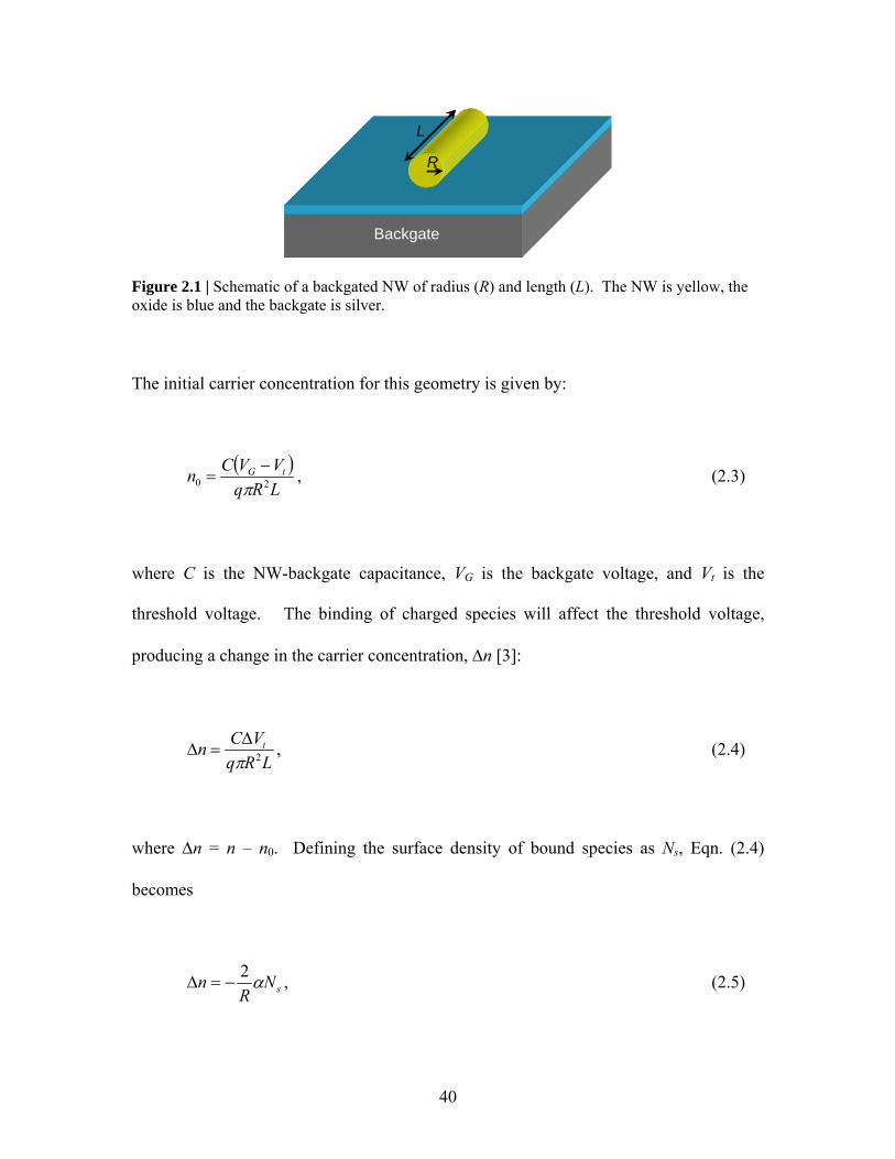
R
L
Backgate
R
L
Backgate
Figure 2.1 | Schematic of a backgated NW of radius (R) and length (L). The NW is yellow, the oxide is blue and the backgate is silver.
The initial carrier concentration for this geometry is given by:
( )LRqVVCn tG
20 π−
= , (2.3)
where C is the NW-backgate capacitance, VG is the backgate voltage, and Vt is the
threshold voltage. The binding of charged species will affect the threshold voltage,
producing a change in the carrier concentration, Δn [3]:
LRq
VCn t2π
Δ=Δ , (2.4)
where Δn = n – n0. Defining the surface density of bound species as Ns, Eqn. (2.4)
becomes
sNR
n α2−=Δ , (2.5)
40
where the charge-transfer coefficient α denotes the number of electrons captured by the
bound molecule. Combining this result with the sensitivity definition in Eqn. (2.1) gives
00,
2nN
RII s
VD
D
DS
α⋅=
Δ . (2.6)
Thus, the NW-FET sensitivity is strongly dependent on device diameter, scaling with the
inverse of the NW radius, for a device of a given length and a constant space charge
density. This demonstrates the importance of minimizing device size in order to
maximize sensitivity, while maintaining high-quality material properties and device
transfer characteristics.
2.2 pH Response
The protonation and deprotonation (and double-protonation) of the silanol groups of
silicon oxide enables properly configured FETs to serve as hydrogen ion sensitive FETs,
or ISFETs [5-7]. We now apply this concept to NW FETs, and explore the dependence
of the electrostatic potential at the device surface (ψ0) on changes in solution pH,
following Ref. 7.
Surface silanol groups can be deprotonated (negative), protonated (neutral), or doubly-
protonated (positive):
41
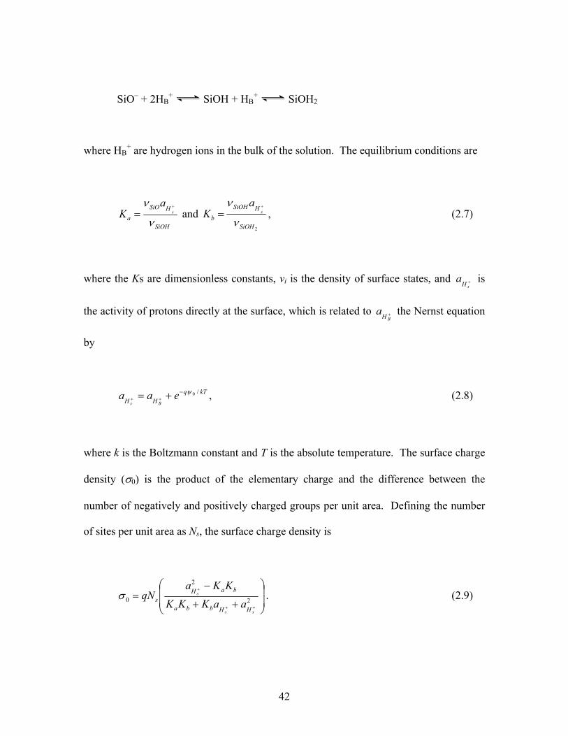
SiO– + 2HB+ SiOH + HB
+ SiOH2
where HB+ are hydrogen ions in the bulk of the solution. The equilibrium conditions are
SiOH
HSiO
as
aK
ν
ν +
= and 2SiOH
HSiOH
bs
aK
ν
ν +
= , (2.7)
where the Ks are dimensionless constants, vi is the density of surface states, and is
the activity of protons directly at the surface, which is related to the Nernst equation
by
+sH
a
+BH
a
, (2.8) kTqHH
eaaBs
/0ψ−+= ++
where k is the Boltzmann constant and T is the absolute temperature. The surface charge
density (σ0) is the product of the elementary charge and the difference between the
number of negatively and positively charged groups per unit area. Defining the number
of sites per unit area as Ns, the surface charge density is
⎟⎟
⎠
⎞
⎜⎜
⎝
⎛
++
−=
++
+
2
2
0
ss
s
HHbba
baHs aaKKK
KKaqNσ . (2.9)
42
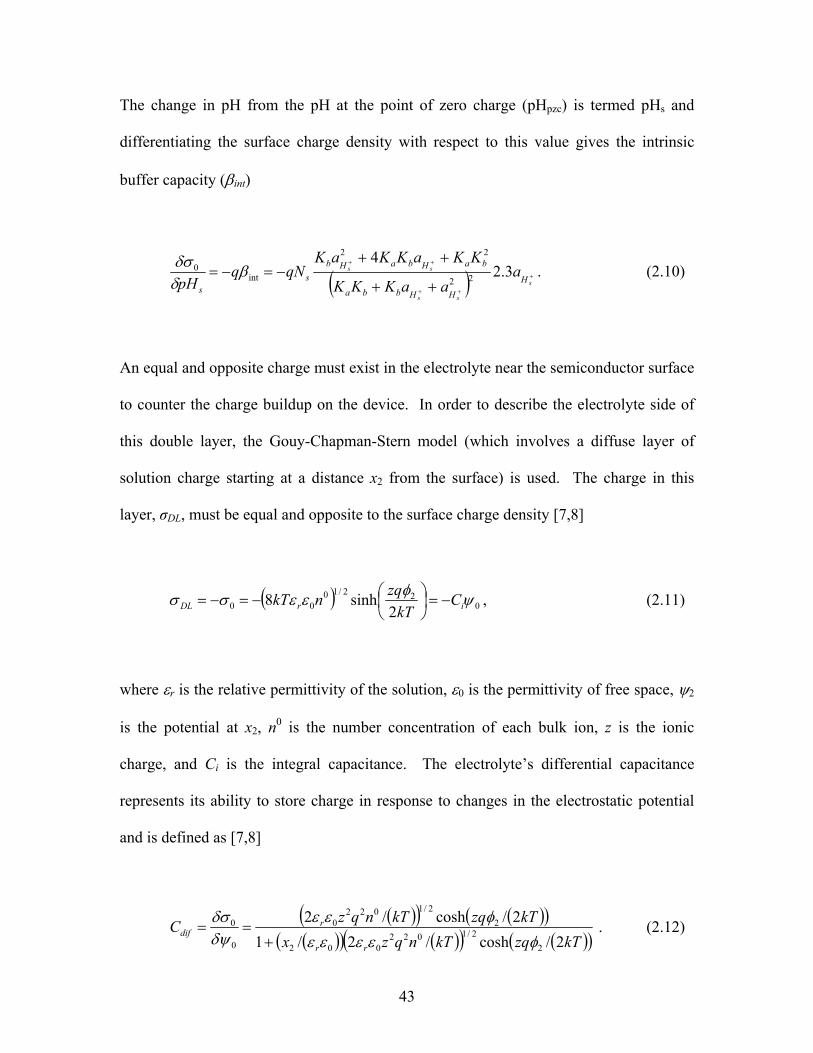
The change in pH from the pH at the point of zero charge (pHpzc) is termed pHs and
differentiating the surface charge density with respect to this value gives the intrinsic
buffer capacity (βint)
( ) +
++
++
++
++−=−=
s
ss
ss
HHHbba
baHbaHbs
s
aaaKKK
KKaKKaKqNq
pH3.2
422
22
int0 β
δδσ . (2.10)
An equal and opposite charge must exist in the electrolyte near the semiconductor surface
to counter the charge buildup on the device. In order to describe the electrolyte side of
this double layer, the Gouy-Chapman-Stern model (which involves a diffuse layer of
solution charge starting at a distance x2 from the surface) is used. The charge in this
layer, σDL, must be equal and opposite to the surface charge density [7,8]
( ) 022/10
00 2sinh8 ψφεεσσ irDL C
kTzqnkT −=⎟
⎠⎞
⎜⎝⎛−=−= , (2.11)
where εr is the relative permittivity of the solution, ε0 is the permittivity of free space, ψ2
is the potential at x2, n0 is the number concentration of each bulk ion, z is the ionic
charge, and Ci is the integral capacitance. The electrolyte’s differential capacitance
represents its ability to store charge in response to changes in the electrostatic potential
and is defined as [7,8]
( )( ) ( )( )( )( ) ( )( ) ( )( )kTzqkTnqzx
kTzqkTnqzCrr
rdif
2/cosh/2/12/cosh/2
22/1022
002
22/1022
0
0
0
φεεεεφεε
δψδσ
+== . (2.12)
43
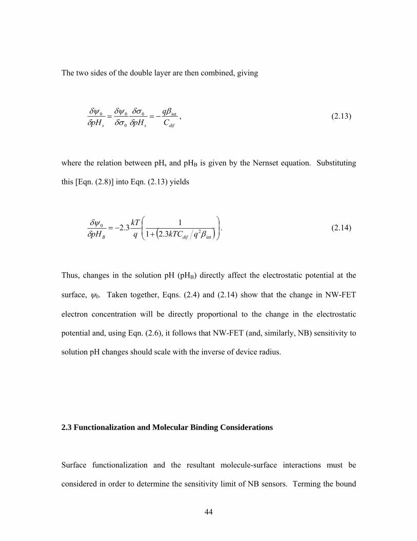
The two sides of the double layer are then combined, giving
difss C
qpHpH
int0
0
00 βδδσ
δσδψ
δδψ
−== , (2.13)
where the relation between pHs and pHB is given by the Nernset equation. Substituting
this [Eqn. (2.8)] into Eqn. (2.13) yields
( )⎟⎟⎠
⎞⎜⎜⎝
⎛
+−=
int2
0
3.2113.2
βδδψ
qkTCqkT
pH difB
. (2.14)
Thus, changes in the solution pH (pHB) directly affect the electrostatic potential at the
surface, ψ0. Taken together, Eqns. (2.4) and (2.14) show that the change in NW-FET
electron concentration will be directly proportional to the change in the electrostatic
potential and, using Eqn. (2.6), it follows that NW-FET (and, similarly, NB) sensitivity to
solution pH changes should scale with the inverse of device radius.
2.3 Functionalization and Molecular Binding Considerations
Surface functionalization and the resultant molecule-surface interactions must be
considered in order to determine the sensitivity limit of NB sensors. Terming the bound
44
molecular species the receptor and the solution-phase molecule the ligand, it is critical to
understand the number of receptors present, the number of ligands introduced, and the
resultant potential for binding events to occur. This section treats this problem by
considering only functionalized surface area and the next section adds fluid flow
considerations.
To the best of our knowledge, all previous silicon NW-FET sensing studies relied on
hydroxyl-reactive schemes for device functionalization [9-15]. These approaches require
the formation of a covalent bond between a surface oxygen atom (present at the silicon
oxide surface) and the silicon atom in the functionalization molecule [16]. This reaction
mechanism will thereby functionalize all silicon oxide surfaces (and most oxide surfaces
in general [16]); since most NW-FET device embodiments [9-15] use an underlying
silicon oxide layer, the entire wafer surface area—not only the NW-FETs—will be
functionalized. Thus, it is imperative to consider binding competition in order to assess
the number of molecules that will reach the NB surface.
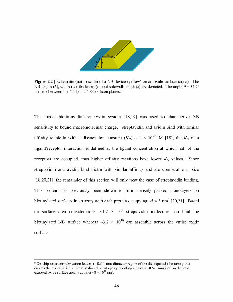
We begin by determining the relative surface area of a NB (yellow, Fig. 2.2) to that of the
NB plus the exposed underlying oxide (yellow and aqua regions, Fig. 2.2). On each die,
the NB surface area‡ is 3 × 10⁷ nm2, whereas the total exposed chip surface area§ is ~8 ×
1011 nm2. Thus, the ratio of exposed oxide to device surface area is ~25,000 : 1.
‡ For a typical NB, w = 50 nm, L = 20 μm, and t = 40 nm. Since we wish to determine the total surface area, we convert the thickness to the sidewall length, s ~ 50 nm, using θ = 54.7º for the angle between the (100) and (111) planes [17] (see Chap. 3 for device fabrication explanation and details). Thus, for a single 2-point device, the surface area is 3 × 10⁶ nm2. However, each die contains four devices, each with four or six leads, so there is approximately tenfold this device surface area exposed per die, 3 × 10⁷ nm2.
45
w
ts
L
θ
w
ts
L
θ
Figure 2.2 | Schematic (not to scale) of a NB device (yellow) on an oxide surface (aqua). The NB length (L), width (w), thickness (t), and sidewall length (s) are depicted. The angle θ = 54.7º is made between the (111) and (100) silicon planes.
The model biotin-avidin/streptavidin system [18,19] was used to characterize NB
sensitivity to bound macromolecular charge. Streptavidin and avidin bind with similar
affinity to biotin with a dissociation constant (KD) ~ 1 × 10-15 M [18]; the KD of a
ligand/receptor interaction is defined as the ligand concentration at which half of the
receptors are occupied, thus higher affinity reactions have lower KD values. Since
streptavidin and avidin bind biotin with similar affinity and are comparable in size
[18,20,21], the remainder of this section will only treat the case of streptavidin binding.
This protein has previously been shown to form densely packed monolayers on
biotinylated surfaces in an array with each protein occupying ~5 × 5 nm2 [20,21]. Based
on surface area considerations, ~1.2 × 10⁶ streptavidin molecules can bind the
biotinylated NB surface whereas ~3.2 × 10¹⁰ can assemble across the entire oxide
surface.
§ On-chip reservoir fabrication leaves a ~0.5-1 mm-diameter region of the die exposed (the tubing that creates the reservoir is ~2.0 mm in diameter but epoxy puddling creates a ~0.5-1 mm rim) so the total exposed oxide surface area is at most ~8 × 10¹¹ nm2.
46
At a streptavidin concentration of 10 fM, the lowest used in our sensing measurements
[19], a 100 μL volume contains ~6 × 10⁵ molecules. At this (and higher) concentrations,
each streptavidin molecule can be assumed to nonreversibly bind the biotinylated surface
due to KD ~ 1 fM. Additionally, the KD of a surface-bound-receptor/ligand interaction is
well below that of the solution-phase KD for the same species due primarily to the
enhancement of the ligand concentration near the surface as a result of bound
receptor/ligand pairs [22-24]. Thus, the nonreversible binding assumption is valid for a
10 fM streptavidin concentration.
Because of the relative surface area considerations, a functionalization scheme that
biotinylates all oxide surfaces yields a ~1/25000 chance that a streptavidin molecule will
bind specifically on the NB. Assuming all molecules bind with equal affinity (neglecting
potential complications of nanoscale seeding affects [25]), a binomial distribution can be
used to estimate the probability of the number of molecules binding on the NB:
knk ppknk
npnkf −−−
= )1()!(!
!),;( , (2.15)
where n is the number of molecules (6 × 10⁵), p is the probability of NB binding
(0.0004), and k is the number of molecules bound to the NB. Using these values, it is
most likely that k ~ 240 streptavidin molecules will bind, which represents only ~2%
coverage of the NB surface area. Thus it is clear that nonspecific functionalization
undermines the benefits of nanoscale-induced sensitivity by preventing effective
molecule-sensor binding. This finding led us to pursue a silicon-specific
47
functionalization technique, which was employed for concentration critical measurements
[19].
The case of specific protein-protein recognition with selectively functionalized NBs is
considered next, using the immunoglobulin G (IgG) system [27]. The ~10 × 10 nm2
[18,26] molecular footprint of anti-IgG antibodies (the receptors) enables at most ~3 ×
105 molecules to bind on all NB surfaces. It should be noted that the maximum number
of bound IgG molecules (the ligands) is expected to be significantly lower due to the
shielding of receptor binding sites due to the random attachment of the receptors during
covalent functionalization [24]—only antibodies with accessible F(ab’)2 domains will
successfully bind antigens [27]. At the 100 fM IgG concentration used in our sensing
measurements [19], a 100 μL volume contains ~6 × 10⁶ molecules. The solution-phase
KD of anti-IgG/IgG interaction is ~10-9 M [27], implying that only ~1 in 5 × 10⁴ or ~120
molecules will be bound**. The number of bound IgGs should be significantly greater
because of the decrease in KD at the sensor surface [22-24]. Thus, provided a silicon-
specific functionalization approach is utilized, it can be assumed that IgGs will bind to all
exposed anti-IgG receptors on the NBs.
Although specific functionalization is desirable for maximum sensitivity, there are
numerous applications where ultrasensitivity is unnecessary, and thus a nonspecific
functionalization approach [28] can be used. Because previous considerations implied a
decrease in sensitivity by ~1/25000, we reduced the available silicon oxide surface area
** Nonreversible binding can be assumed for this system on timescales of ~1-10 mins [24].
48
by selective masking [28], and achieved a 1/333 relative ratio††. We now apply this
approach to a test system, complementary DNA pairing, and demonstrate that a 10 pM
concentration is sufficient for NB sensing. One-hundred microliters of 10 pM probe
single stranded- (ss)-DNA (complementary to a surface-bound ss-DNA) was added, thus
~3 × 10⁹ molecules were present. Since DNA hybridization can be assumed to be
nonreversible at room temperature‡‡, there should be a ~33% coverage of the NB surface;
assuming a DNA 20-mer footprint of ~2.5 × 2.5 nm2, it follows that ~1.6 × 10⁵ molecules
of ~4.8 × 10⁶ possible molecules will be bound.
Taken together, these data demonstrate that silicon-specific functionalization approaches
are critical to achieve femtomolar ligand detection with NB sensors, though nonspecific
functionalization is adequate for sensing picomolar ligand concentrations.
2.4 Chamber Design and Solution Exchange Considerations
In the above section we assumed that all ligands present after solution exchange would be
available to bind to the sensor surface. Previous studies with NW-FET sensing relied on
microchannels [29] for solution exchange [9-15] but theoretical studies suggested that
mass transport [30] in such systems would be diffusion-limited due to the laminar flow †† Thus, we protected the oxide surface with layer of photoresist and opened ~50 × 50 μm2 vias over active devices, leaving a functionalized surface area of ~1 × 10¹⁰ nm2 per die. ‡‡ The energy of a hydrogen bond is 1-5 kcal/mol [30], there are 2.5 hydrogen bonds per DNA basepair (2
for A-T, 3 for G-C), and we used a 20-mer, so: 37)300)(987.1()20)(5.2)(101(
10~3
−×−
= eKD .
49

through the microchannels [31,32]. We first apply the analytical solutions obtained by
the authors in Refs. 31 and 32 to the case of NB sensors and show that microfluidic
systems are impractical for nanosensors. We then discuss the theory behind our fluid
handling design and demonstrate that this setup is ideal for molecular transport to the
NBs.
The accumulation of molecules on the surface of a NW (approximated as a hemicylinder
of length L and radius a) based on solution flow through a microchannel above the device
(Fig. 2.3) is given by [31]
∫∞ −
+−
=0
320
20
0
)()(14)(
2
udu
auYauJeCLNtN
tDuA
π, (2.16)
where J0 and Y0 are Bessel functions, NA is Avogadro’s number, D is the diffusion
coefficient, the C0 is the ligand concentration.
Figure 2.3 | Schematic (not to scale) of a NW (red) in a flow channel. The arrows indicate the direction of flow.
Equation (2.16) is solved analytically in Refs. 31 and 32 to yield the molecular flux to the
NW surface:
50
( ) ( )⎟⎟⎠
⎞⎜⎜⎝
⎛−
−⎟⎟⎠
⎞⎜⎜⎝
⎛−
=s
s
sA Pn
PPn
CDLNJll 885.4
09266.01885.4
20
π , (2.17)
for Ps < 1, where
2
26DwhQWPs = . (2.18)
Here, Q is the volumetric flow rate, w is the width of the microchannel, h is the
microchannel height, and W = πa [31]. Using D = 150 μm2/s [31], L = 20 μm, a = 25
nm, w = 500 μm, and h = 100 μm to best approximate the NB geometry, we plot the
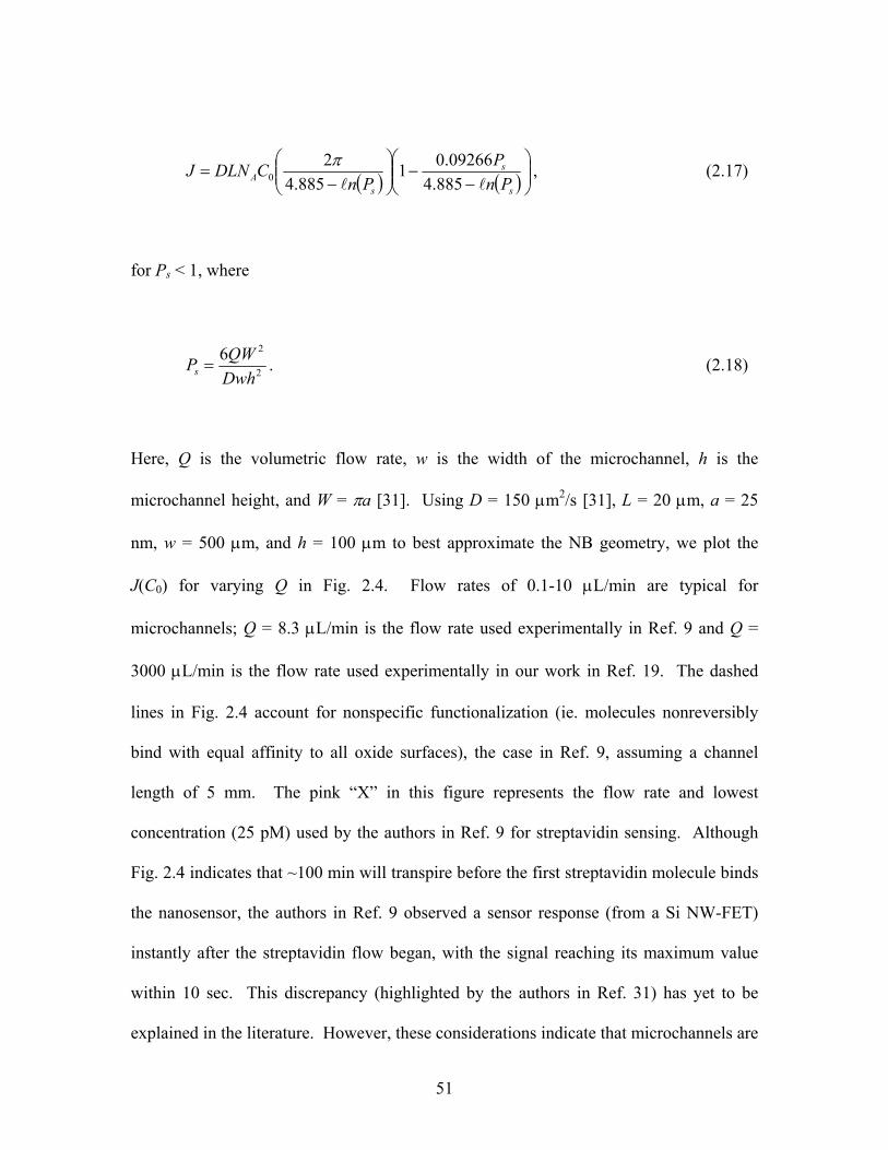
J(C0) for varying Q in Fig. 2.4. Flow rates of 0.1-10 μL/min are typical for
microchannels; Q = 8.3 μL/min is the flow rate used experimentally in Ref. 9 and Q =
3000 μL/min is the flow rate used experimentally in our work in Ref. 19. The dashed
lines in Fig. 2.4 account for nonspecific functionalization (ie. molecules nonreversibly
bind with equal affinity to all oxide surfaces), the case in Ref. 9, assuming a channel
length of 5 mm. The pink “X” in this figure represents the flow rate and lowest
concentration (25 pM) used by the authors in Ref. 9 for streptavidin sensing. Although
Fig. 2.4 indicates that ~100 min will transpire before the first streptavidin molecule binds
the nanosensor, the authors in Ref. 9 observed a sensor response (from a Si NW-FET)
instantly after the streptavidin flow began, with the signal reaching its maximum value
within 10 sec. This discrepancy (highlighted by the authors in Ref. 31) has yet to be
explained in the literature. However, these considerations indicate that microchannels are
51
ineffective at bringing sufficient numbers of molecules to nanosensor surfaces and led us
to design a different setup for solution exchange.
10-15 10-14 10-13 10-12 10-11 10-10 10-91E-6
1E-4
0.01
1
100
10000
1000000
1E8
1E10
1E12#
Mol
ecul
es/M
in
C0 (M)
XX
XX
Silicon-specificfunctionalization
Nonspecificfunctionalization
Ref. 9
Our work
10-15 10-14 10-13 10-12 10-11 10-10 10-91E-6
1E-4
0.01
1
100
10000
1000000
1E8
1E10
1E12#
Mol
ecul
es/M
in
C0 (M)
XX
XX
Silicon-specificfunctionalization
Nonspecificfunctionalization
Ref. 9
Our work
Figure 2.4 | Theoretical plot of the number of molecules per minute irreversibly binding to a representative NB surface in a flow channel versus ligand concentration. The flow rates are listed. The pink and purple X’s denotes the experimental parameters used by the authors in Ref. 9 and us in Ref. 19, repectively, for the lowest limit of streptavidin detection.
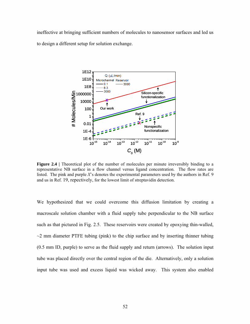
We hypothesized that we could overcome this diffusion limitation by creating a
macroscale solution chamber with a fluid supply tube perpendicular to the NB surface
such as that pictured in Fig. 2.5. These reservoirs were created by epoxying thin-walled,
~2 mm diameter PTFE tubing (pink) to the chip surface and by inserting thinner tubing
(0.5 mm ID, purple) to serve as the fluid supply and return (arrows). The solution input
tube was placed directly over the central region of the die. Alternatively, only a solution
input tube was used and excess liquid was wicked away. This system also enabled
52
continual mixing (equivalent to pippetting up-and-down) throughout the course of
sensing measurements.
aa
Figure 2.5 | a, Schematic of the solution chamber (~2 mm diameter) superimposed on an optical micrograph of a section of wafer containing multiple devices. Rigid, thin-walled tubing (pink) creates a reservoir into which softer, Tygon tubing (purple) serves as the fluid supply and return (arrows). b, Optical micrograph of a NB sensor array with fluid reservoir attached and source and drain contacted.
The flux of molecules to a surface is given by the mass transport equation:
020
2
Cudz
CdDJ zz +−= , (2.18)
where uz is the velocity in the z-direction. Since the solution flow is perpendicular to the
sensor surface, we hypothesized that convection and not diffusion would be the primary
determinant of mass-transport. In order to validate this, we calculated the Schmidt and
Reynolds numbers for the system [30]. The Schmidt number, defined as u/D, gives the
ratio of viscous to diffusive transport and is a property of the fluid/solute system. For
proteins in aqueous solutions, is number is ~104-105 [30]. The Reynolds number, u·d/v,
53
where d is the tube diameter and v is the kinematic viscosity, gives the ratio of inertial to
viscous forces and is system-specific [30]. A solution exchange rate of 50 μL/s (3000
μL/min) was used for sensing measurements, yielding a Reynolds number of 125 for the
0.5 mm-diameter input tube. Taken together, these values suggest that diffusion can be
neglected in this system due to the fact that the perpendicular convection will bring all
molecules directly to the sensor surface. Thus, we simplify Eqn. (2.18) to:
. (2.19) 0CuJ zz =
Because we are only considering flow in the z-direction and have neglected diffusion, we
must account for the fact that the NBs cover only 0.0015% of the cross-sectional area of
the inlet tube by multiplying the right-hand side of Eqn. (2.19) by this factor. We plot
J(C0) for Q = 3000 μL/min in Fig. 2.4 (solid cyan line). These data indicate that we have
overcome the diffusion limitation inherent in microchannels and have successfully
created a fluid-exchange system that can rapidly transport a sufficient number of
molecules to the NB surface to enable sensing within seconds.
2.5 Debye Screening Considerations
As described above, NW-FET and NB sensors work similarly to conventional chemical
field effect transistors (chemFETs) [5-7], sensing the presence of bound species by their
intrinsic charge [1,9-15,19]. When specific receptor molecules (ie. biotin, antibodies,
54
ssDNA) are conjugated to the NB surface in order to sense specific ligands, the ligands
are removed from the sensor surface by at least the length of the receptor, generally 10-
100 Å. Since the receptors are dissolved in the solution, an understanding of the
screening of molecular charge by dissolved ions (Debye screening) is paramount to
interpreting device results. The charge of solution-based molecules and macromolecules
is screened by dissolved ions: a negative species such as streptavidin or DNA will be
surrounded by positively charged ions due to electrostatic interactions. Beyond a certain
distance, termed the Debye length (λD), Coulomb interactions can be ignored because the
positively-charged cloud of ions will cancel out the negative charge inherent to the DNA,
rendering the species charge-neutral [33]. Thus, at distances beyond λD, the molecular
charge is effectively screened by the dissolved ions. For aqueous solutions at room
temperature, this length is given by
∑
=
iiiB
Dzl 24
1ρπ
λ , (2.20)
where lB is the Bjerrum length = 0.7 nm, ΣB i is the sum over all ion species, and ρi and zi
are the density (6.02 × 10 cm ) and the valence, respectively, of ion species i [ ]. In
our sensing measurements we used dilutions of phosphate buffered saline (PBS); these
dilutions were made relative to 1X PBS, which contains 150 mM NaCl, 3 mM KCl, and
10 mM phosphate salts (monobasic and dibasic). The calculated values of λ
20 -3 33
D for the five
solutions used in sensing measurements are given below in Table 2.1. These values show
that for functionalized NW-FET and NB measurements (those relying on a receptor-
55
ligand binding event), careful consideration must be given to buffer ionic strength so as
not to screen the ligand.
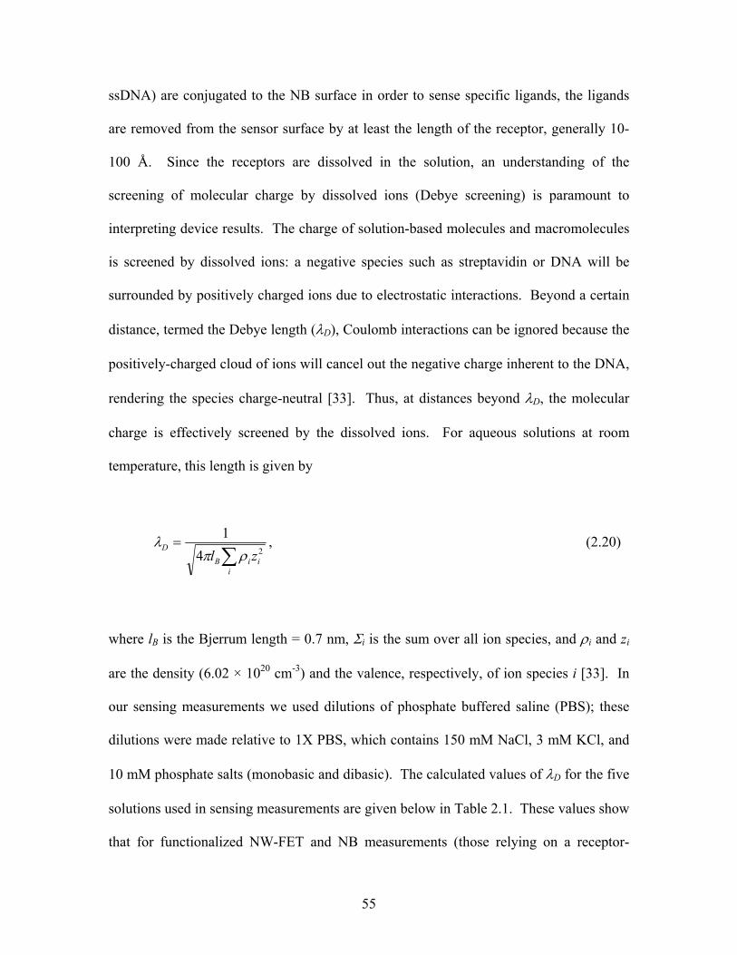
[PBS] λD (nm)
1X 0.7 0.1X 2.3 0.05X 3.3 0.01X 7.3 0.001X 23.2 Table 2.1 | Calculated Debye screening lengths (λD) for varying concentrations of PBS.
2.6 Conclusions
These theoretical analyses highlighted four primary considerations for our experimental
setup. First, in order to maximize sensitivity (pH and otherwise) we had to minimize the
cross-sectional area of the sensor. This consideration led to the design and realization of
the NBs, discussed in Chap. 3. Second, to harness the NB’s potential sensitivity based on
scaling, it was critical to develop a silicon-specific functionalization scheme, which is
described in Chap. 4. Third, a solution-exchange system other than a microchannel was
necessary to deliver the required number of molecules to enable rapid, ultrasensitive NB
sensing. We addressed this constraint by creating the reservoir described above. Fourth,
the Debye screening study highlighted the importance of choosing appropriate buffers for
sensing measurements, a point that is considered throughout the sensing measurements
described in Chap. 5.
56
References
1. Patolsky, F., Zheng, G. & Lieber, C. M. Nanowire-based biosensors. Anal. Chem.
78, 426-4269 (2006).
2. Kranti, A., Rashmi, Haldar, S. & Gupta, R. S. Design and optimization of vertical
surrounding gate MOSFETs for enhanced transconductance-to-current ratio
(gm/Ids). Solid-State Elec. 47, 155-159 (2003).
3. Fan, Z. & Lu, J. G. Gate-refreshable nanowire chemical sensors. Appl. Phys. Lett.
86, Art. No. 123510 (2005).
4. Fan, Z. & Lu, J. G. Chemical sensing with ZnO nanowire field-effect transistor.
IEEE Trans. Nanotech. 5, 393-396 (2006).
5. Dzyadevych, S. V. et al. Biosensors based on enzyme field-effect transistors for
determination of some substrates and inhibitors. Anal. Bioanal. Chem. 377, 496-
506 (2003).
6. Bousse, L., de Rooij, N. F. & Bergveld, P. Operation of chemically sensitive
field-effect sensors as a function of the insulator-electrolyte interface. IEEE
Trans. Elect. Dev. ED-30, 1263-1270 (1983).
7. van Hal, R. E. G., Eijkel, J. C. T. & Bergveld, P. A novel description of ISFET
sensitivity with the buffer capacity and double-layer capacitance as key
parameters. Sens. Act. B 24-25, 201-205 (1995).
8. Yates, D. E., Levine, S. & Healy, T. W. Site-binding model of the electrical
double layer at the oxide/water interface. J. Chem. Soc. Faraday Trans. 70, 1807-
1818 (1974).
57
9. Cui, Y., Wei, Q., Park, H. & Lieber, C. M. Nanowire nanosensors for highly
sensitivie and selective detection of biological and chemical species. Science 293,
1289-1292 (2001).
10. Wang, W. U., Chen, C., Lin, K.-h., Fang, Y. & Lieber, C. M. Label-free detection
of small-molecule-protein interactions by using nanowire nanosensors. Proc. Nat.
Acad. Sci. 102, 3208-3212 (2005).
11. Zheng, G., Patolsky, F., Cui. Y., Wang, W. U. & Lieber, C. M. Multiplexed
electrical detection of cancer markers with nanowire sensor arrays. Nat. Biotech.
23, 1294-1301 (2005).
12. Hahm, J.-i. & Lieber, C. M. Direct ultrasensitivie electrical detection of DNA and
DNA sequence variations using nanowire nanosensors. Nano Lett. 4, 51-54
(2004).
13. Li, Z., Chen, Y., Li, X., Kamins, T. I., Nauka, K., & Williams, R. S. Sequence-
specific label-free DNA sensors based on silicon nanowires. Nano Lett. 4, 245-
247 (2004).
14. Cheng, M. M.-C. et al. Nanotechnologies for biomolecular detection and medical
diagnostics. Curr. Op. Chem. Biol. 10, 11-19 (2006).
15. Patolsky, F., Zheng, G., Hayden, O., Lakadamyali, M., Zhuang, X. & Lieber, C.
M. Electrical detection of single viruses. Proc. Nat. Acad. Sci. 101, 14017-14022
(2004).
16. Filler, M. A. & Bent, S. F. The surface as molecular reagent: organic chemistry at
the semiconductor interface. Prog. Surf. Sci. 73, 1-56 (2003).
58
17. Madou, M. J. Fundamentals of Microfabrication. 2nd Edn. (CRC, New York,
2002).
18. Hermanson, G. T. Bioconjugate Techniques (Elsevier Science & Technology
Books, New York, 1996).
19. Stern, E. et al. Label-free immunodetection with CMOS-compatible
semiconducting nanowires. Nature 445, 519-522 (2007).
20. Avila-Sakar, A. J. & Chiu, W. Visualization of β-sheets and side-chain clusters in
two-dimensional periodic arrays of streptavidin on phospholipids monolayers by
electron crystallography. Biophys. J. 70, 57-68 (1996).
21. Darst, S. A. et al. Two-dimensional crystals of streptavidin on biotinylated lipid
layers and their interactions with biotinylated macromolecules. Biophys. J. 59,
387-396 (1991).
22. Andersen, P. S., Menne, C., Mariuzza, R. A., Geisler, C. & Karjalainen, K. A
response calculus for immobilized T cell receptor ligands. J. Biol. Chem. 276,
49125-49132 (2001).
23. Bell, G. I. Models for the specific adhesion of cells to cells. Science 200, 618-627
(1978).
24. O’Shannessy, D. J. & Winzor, D. J. Interpretation of deviations from pseudo-first-
order kinetic behavior in the characterization of ligand binding to biosensor
technology. Anal. Biochem. 236, 275-283 (1996).
25. Gupta, A. K. et al. Anomalous resonance in a nanomechanical biosensor. Proc.
Natl. Acad. Sci. U.S.A. 103, 13362-13367 (2006).
59
26. Chiu, W., Avila-Sakar, A. J. & Schmid, M. F. Electron crystallography of
macromolecular periodic arrays on phospholipids monolayers. Adv. Biophys. 34,
161-172 (1997).
27. Voet, D. & Voet, J. G. Biochemistry. 2nd Edn. (John Wiley & Sons, New York,
1995).
28. Stern, E. et al. Critical dependence of nanowire field effect transistors on Debye
screening length. Manuscript in preparation.
29. Duffy, D. C., McDonald, J. C., Schueller, O. J. A. & Whitesides, G. M. Rapid
prototyping of microfluidic systems in poly(dimethylsiloxane). Anal. Chem. 70,
4974-4984 (1998).
30. Truskey, G. A., Yuan, F. & Katz, D. F. Transport Phenomena in Biological
Systems. (Pearson Prentice Hall, New Jersey, 2004.)
31. Sheehan, P. E. & Whitman, L. J. Detection limits for nanoscale biosensors. Nano
Lett. 5, 803-807 (2005).
32. Zhang, W., Stone, H. A. & Sherwood, J. D. Mass transfer at a microelectrode in
channel flow. J. Phys. Chem. 100, 9462-9464 (1996).
33. Israelachvili, J. Intermolecular & Surface Forces. 2nd Ed. (Academic Press,
London, 1991).
60
Chapter 3: Nanobar Fabrication and Characterization
3.1 Nanobar Fabrication [19]
In order to avoid the integration and fabrication issues inherent with grown, bottom-up-
fabricated NW devices [1-18], we designed a process to create semiconducting NWs—
termed nanobars (NBs)—with a traditional, top-down approach [19]. Although top-
down approaches have been demonstrated previously [20-26], those configured for
sensing showed disappointing performance in previous studies [20,21], most likely due to
process-induced material degradation. We used ultra-thin silicon-on-insulator (UT-SOI)
wafers as starting substrates [20,21,27], since these require only lateral (i.e., in-plane, 2D)
active layer definition to achieve the nanometer dimensions needed for a NW-type device
[17,18]. In order to avoid reactive-ion etching (RIE) [28] of the active silicon layer,
which unacceptably degraded device performance [20,21], but achieve the nanometer-
scale dimensions necessary for sensitivity [19], we developed a fabrication process using
an anisotropic wet etch {specifically, tetramethylammonium hydroxide, TMAH, which
etches Si (111) planes ~100 times more slowly than all other planes [17,18,29]}. This
approach allows retention of pattern definition (of a masking oxide layer), and smoothes
edge imperfections not aligned to the (111) plane [17,18]. Previous work on TMAH-
defined electronic devices [30] has shown excellent retention of electrical properties
[17,31], although not in configurations suitable for sensing. This approach uses
commercially available materials {(100) SOI wafers [32]} which yield trapezoidal cross-
61
section NWs with dominant Si (111) exposed planes, the preferred surface for selective
surface functionalization [32].
Devices used in this work were fabricated from three SOI wafers, with active Si layers
thinned to 25, 40, 80 nm by iterative oxidation/wet etching steps. We chose these
thicknesses because previous studies had shown that the transport properties of active
silicon layers are constant throughout this range [33]. All wafers were UNIBOND SOI
[27] but two sets were used: 4” wafers purchased from Silicon Quest were used for the 40
and 80 nm devices, while 8” SOI wafers purchased from SOITEC USA (and laser cut to
4” by Silicon Quest) were used for the 25 nm devices. No significant difference in
device quality was observed between the two wafer sets.
The fabrication steps are outlined in Fig. 3.1. Wafers were RCA cleaned prior to
oxidation steps and were cleaned with 3:1 sulfuric acid:hydrogen peroxide (piranha) prior
to all other lithographic steps save the final step, prior to which they were cleaned with
acetone and methanol [28]. All optical masks were purchased from Benchmark
Technologies (it should be noted that experimental design utilizied transparency masks
purchased from Cad Art Services, Inc.) and all optical lithographic steps were performed
using either an EV Group 600 or 620. In Step 1, the active layer of the wafer was thinned
to the desired height by subsequent wet thermal oxidation (MRL Industries Furnace) and
wet chemical etching. The active silicon thickness at this point was ~20 nm thicker than
the final desired thickness to account for the silicon thinning inherent in the masking
oxide growth (Step 5).
62
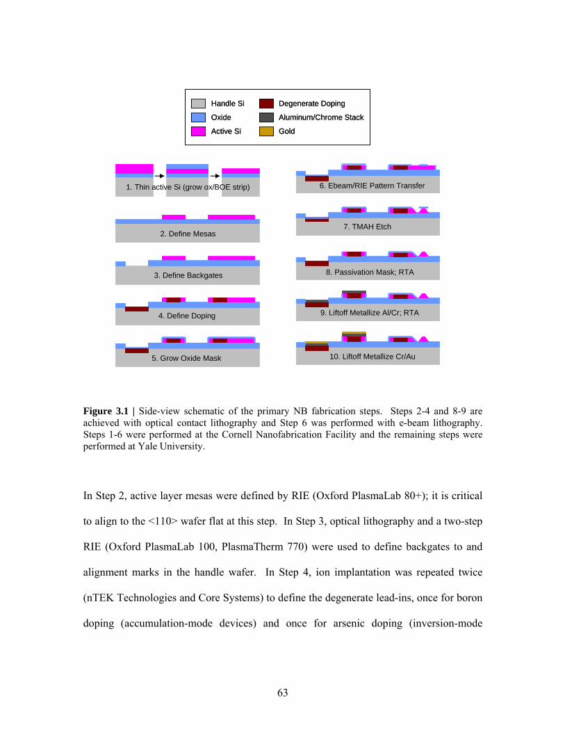
2. Define Mesas
4. Define Doping 9. Liftoff Metallize Al/Cr; RTA
10. Liftoff Metallize Cr/Au
7. TMAH Etch
6. Ebeam/RIE Pattern Transfer
8. Passivation Mask; RTA
5. Grow Oxide Mask
3. Define Backgates
1. Thin active Si (grow ox/BOE strip)
Handle Si
Oxide
Active Si
Degenerate Doping
Aluminum/Chrome Stack
Gold
Handle Si
Oxide
Active Si
Degenerate Doping
Aluminum/Chrome Stack
Gold
Figure 3.1 | Side-view schematic of the primary NB fabrication steps. Steps 2-4 and 8-9 are achieved with optical contact lithography and Step 6 was performed with e-beam lithography. Steps 1-6 were performed at the Cornell Nanofabrication Facility and the remaining steps were performed at Yale University.
In Step 2, active layer mesas were defined by RIE (Oxford PlasmaLab 80+); it is critical
to align to the <110> wafer flat at this step. In Step 3, optical lithography and a two-step
RIE (Oxford PlasmaLab 100, PlasmaTherm 770) were used to define backgates to and
alignment marks in the handle wafer. In Step 4, ion implantation was repeated twice
(nTEK Technologies and Core Systems) to define the degenerate lead-ins, once for boron
doping (accumulation-mode devices) and once for arsenic doping (inversion-mode
63
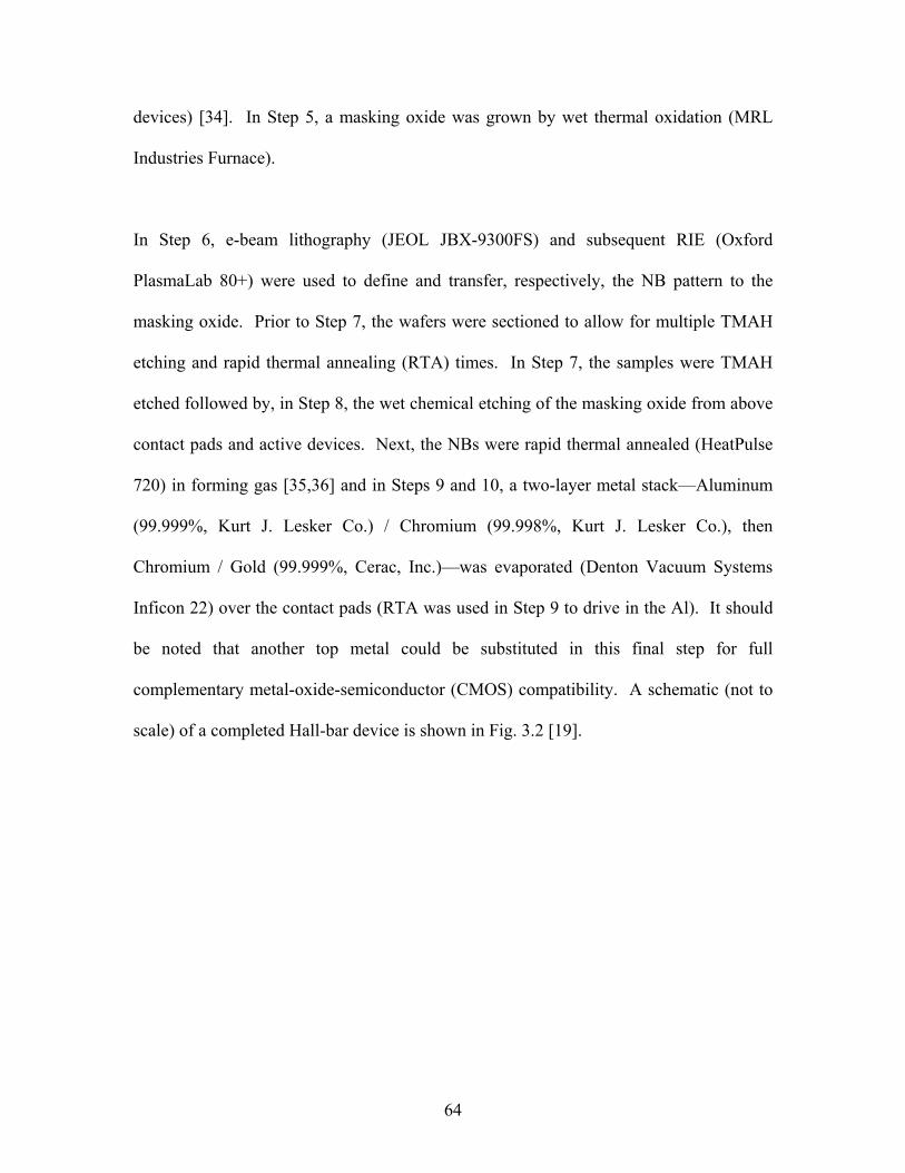
devices) [34]. In Step 5, a masking oxide was grown by wet thermal oxidation (MRL
Industries Furnace).
In Step 6, e-beam lithography (JEOL JBX-9300FS) and subsequent RIE (Oxford
PlasmaLab 80+) were used to define and transfer, respectively, the NB pattern to the
masking oxide. Prior to Step 7, the wafers were sectioned to allow for multiple TMAH
etching and rapid thermal annealing (RTA) times. In Step 7, the samples were TMAH
etched followed by, in Step 8, the wet chemical etching of the masking oxide from above
contact pads and active devices. Next, the NBs were rapid thermal annealed (HeatPulse
720) in forming gas [35,36] and in Steps 9 and 10, a two-layer metal stack—Aluminum
(99.999%, Kurt J. Lesker Co.) / Chromium (99.998%, Kurt J. Lesker Co.), then
Chromium / Gold (99.999%, Cerac, Inc.)—was evaporated (Denton Vacuum Systems
Inficon 22) over the contact pads (RTA was used in Step 9 to drive in the Al). It should
be noted that another top metal could be substituted in this final step for full
complementary metal-oxide-semiconductor (CMOS) compatibility. A schematic (not to
scale) of a completed Hall-bar device is shown in Fig. 3.2 [19].
64
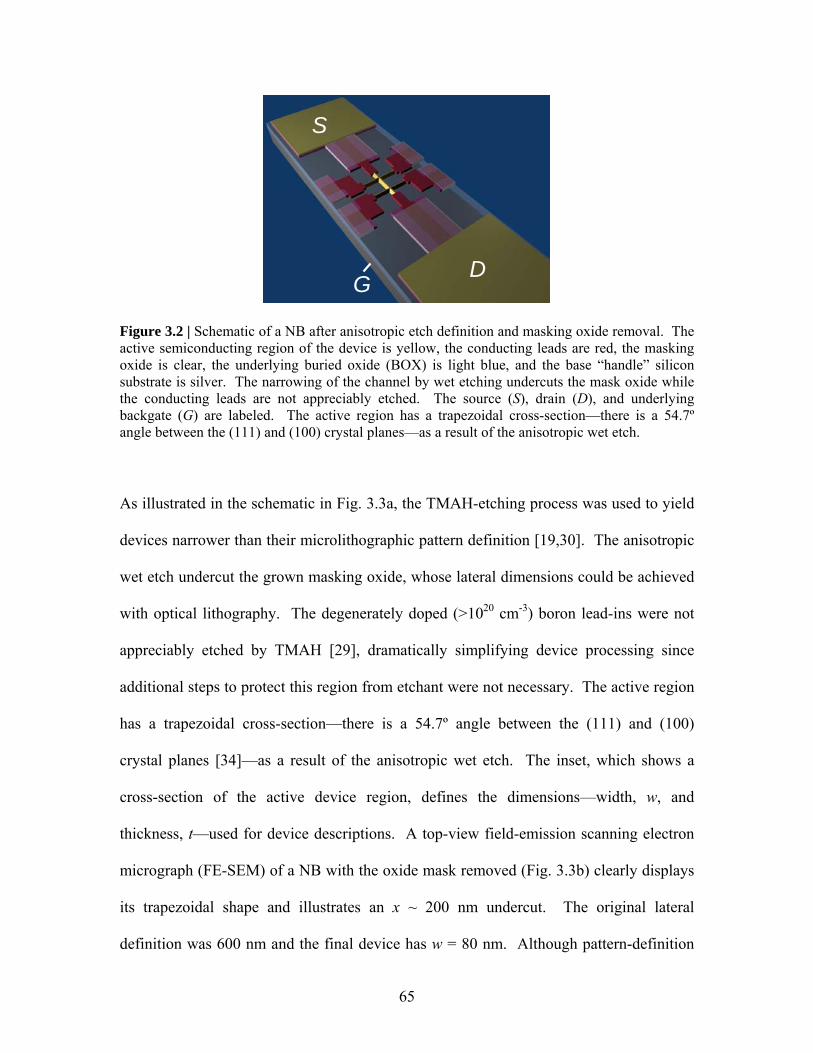
S
DG
S
DG
Figure 3.2 | Schematic of a NB after anisotropic etch definition and masking oxide removal. The active semiconducting region of the device is yellow, the conducting leads are red, the masking oxide is clear, the underlying buried oxide (BOX) is light blue, and the base “handle” silicon substrate is silver. The narrowing of the channel by wet etching undercuts the mask oxide while the conducting leads are not appreciably etched. The source (S), drain (D), and underlying backgate (G) are labeled. The active region has a trapezoidal cross-section—there is a 54.7º angle between the (111) and (100) crystal planes—as a result of the anisotropic wet etch.
As illustrated in the schematic in Fig. 3.3a, the TMAH-etching process was used to yield
devices narrower than their microlithographic pattern definition [19,30]. The anisotropic
wet etch undercut the grown masking oxide, whose lateral dimensions could be achieved
with optical lithography. The degenerately doped (>1020 cm-3) boron lead-ins were not
appreciably etched by TMAH [29], dramatically simplifying device processing since
additional steps to protect this region from etchant were not necessary. The active region
has a trapezoidal cross-section—there is a 54.7º angle between the (111) and (100)
crystal planes [34]—as a result of the anisotropic wet etch. The inset, which shows a
cross-section of the active device region, defines the dimensions—width, w, and
thickness, t—used for device descriptions. A top-view field-emission scanning electron
micrograph (FE-SEM) of a NB with the oxide mask removed (Fig. 3.3b) clearly displays
its trapezoidal shape and illustrates an x ~ 200 nm undercut. The original lateral
definition was 600 nm and the final device has w = 80 nm. Although pattern-definition
65
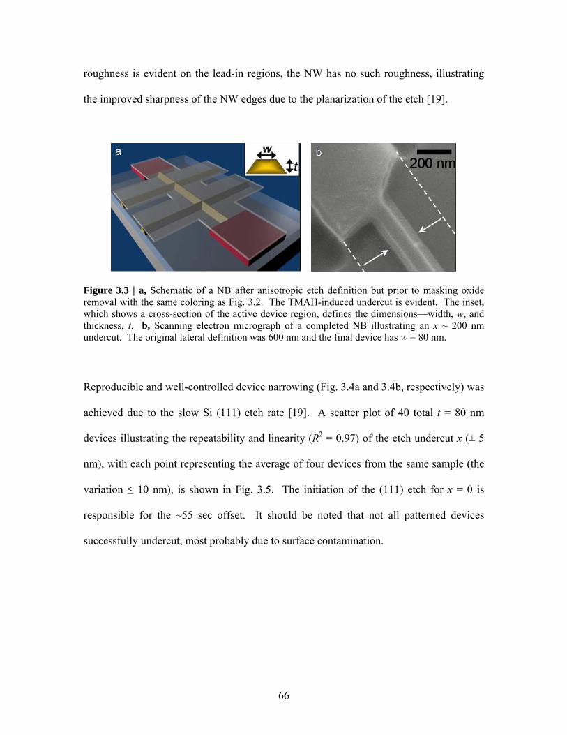
roughness is evident on the lead-in regions, the NW has no such roughness, illustrating
the improved sharpness of the NW edges due to the planarization of the etch [19].
Figure 3.3 | a, Schematic of a NB after anisotropic etch definition but prior to masking oxide removal with the same coloring as Fig. 3.2. The TMAH-induced undercut is evident. The inset, which shows a cross-section of the active device region, defines the dimensions—width, w, and thickness, t. b, Scanning electron micrograph of a completed NB illustrating an x ~ 200 nm undercut. The original lateral definition was 600 nm and the final device has w = 80 nm.
Reproducible and well-controlled device narrowing (Fig. 3.4a and 3.4b, respectively) was
achieved due to the slow Si (111) etch rate [19]. A scatter plot of 40 total t = 80 nm
devices illustrating the repeatability and linearity (R2 = 0.97) of the etch undercut x (± 5
nm), with each point representing the average of four devices from the same sample (the
variation ≤ 10 nm), is shown in Fig. 3.5. The initiation of the (111) etch for x = 0 is
responsible for the ~55 sec offset. It should be noted that not all patterned devices
successfully undercut, most probably due to surface contamination.
66
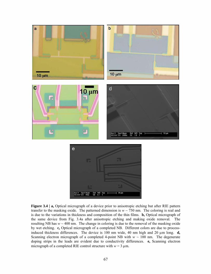
Figure 3.4 | a, Optical micrograph of a device prior to anisotropic etching but after RIE pattern transfer to the masking oxide. The patterned dimension is w ~ 750 nm. The coloring is real and is due to the variations in thickness and composition of the thin films. b, Optical micrograph of the same device from Fig. 3.4a after anisotropic etching and making oxide removal. The resulting NB has w ~ 400 nm. The change in coloring is due to the removal of the masking oxide by wet etching. c, Optical micrograph of a completed NB. Different colors are due to process-induced thickness differences. The device is 100 nm wide, 40 nm high and 20 μm long. d, Scanning electron micrograph of a completed 4-point NB with w ~ 100 nm. The degenerate doping strips in the leads are evident due to conductivity differences. e, Scanning electron micrograph of a completed RIE control structure with w = 3 μm.
67
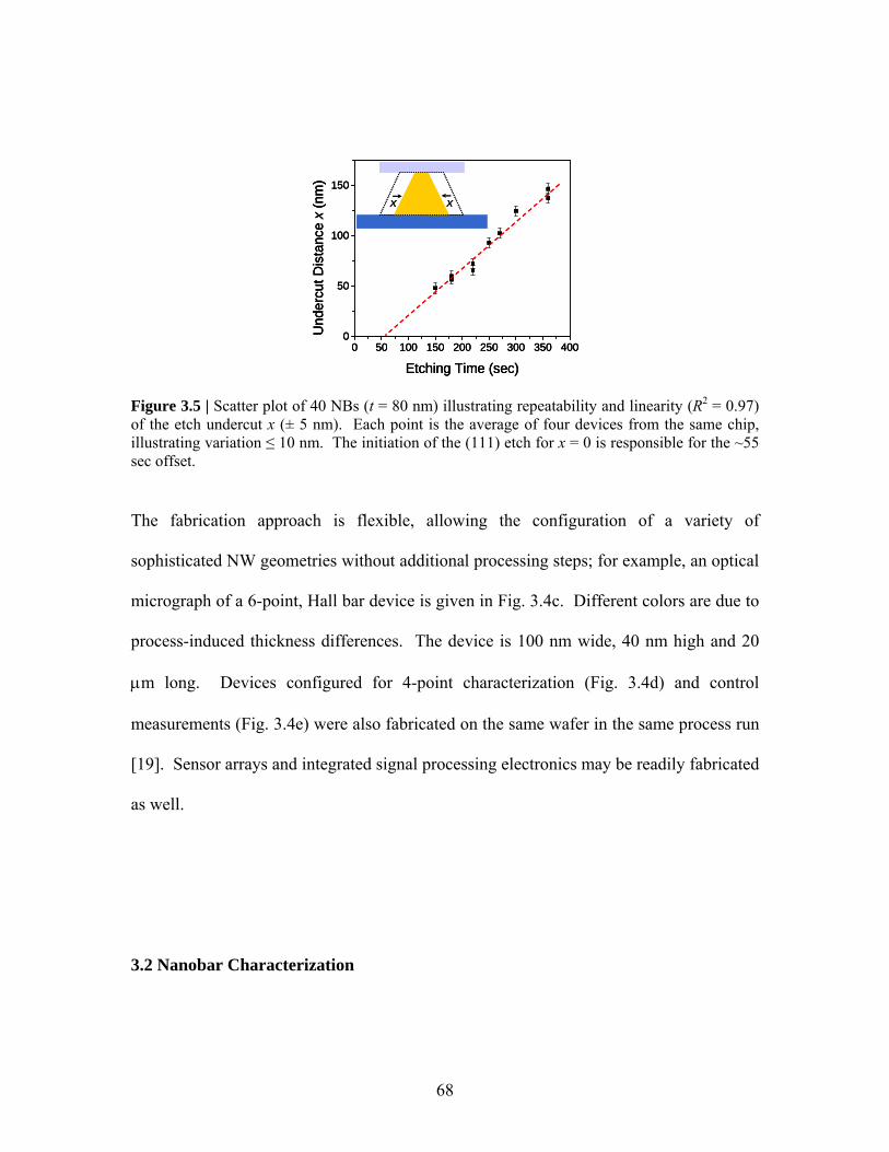
0 50 100 150 200 250 300 350 4000
50
100
150
Und
ercu
t Dis
tanc
e x
(nm
)
Etching Time (sec)
x x
0 50 100 150 200 250 300 350 4000
50
100
150
Und
ercu
t Dis
tanc
e x
(nm
)
Etching Time (sec)0 50 100 150 200 250 300 350 400
0
50
100
150
Und
ercu
t Dis
tanc
e x
(nm
)
Etching Time (sec)
x x
Figure 3.5 | Scatter plot of 40 NBs (t = 80 nm) illustrating repeatability and linearity (R2 = 0.97) of the etch undercut x (± 5 nm). Each point is the average of four devices from the same chip, illustrating variation ≤ 10 nm. The initiation of the (111) etch for x = 0 is responsible for the ~55 sec offset.
The fabrication approach is flexible, allowing the configuration of a variety of
sophisticated NW geometries without additional processing steps; for example, an optical
micrograph of a 6-point, Hall bar device is given in Fig. 3.4c. Different colors are due to
process-induced thickness differences. The device is 100 nm wide, 40 nm high and 20
μm long. Devices configured for 4-point characterization (Fig. 3.4d) and control
measurements (Fig. 3.4e) were also fabricated on the same wafer in the same process run
[19]. Sensor arrays and integrated signal processing electronics may be readily fabricated
as well.
3.2 Nanobar Characterization
68
All electrical measurements were performed with an HP4156B Semiconductor Parameter
Analyzer (SPA). Device transconductance was calculated by the linear best-fit to the
source-drain current-to-source-drain voltage [ISD(VGD)] dependence. The capacitance
was calculated using the measured geometrical parameters. For consistency, all NB
mobilities are calculated in the pre-saturation regime according to [15,34]
SDVGD
SDSD V
IVLC
∂∂
⎟⎠⎞
⎜⎝⎛=
−1
2μ , (3.1)
where
)/4ln(2 0
dhLC πεε
= , (3.2)
L is the source-drain NW length, h is the oxide thickness, d is the NW diameter, and VGD
is the gate-drain voltage.
Electrical characterization verified that the NB fabrication approach produced high
quality semiconducting devices. The ISD(VSD) dependencies for varying VGD are given in
Figs. 3.6a and 3.6b for representative p-type and n-type devices, respectively. Figure
3.6a shows the ISD(VSD) dependence for varying VGD from 0 to -40V in -1V steps
(indicated by the red arrow) for a (w = 50 nm, t = 25 nm) device, demonstrating p-type
accumulation mode behavior. Figure 3.6b shows the ISD(VSD) dependence for varying
69
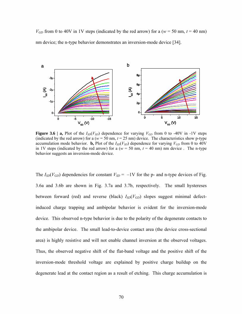
VGD from 0 to 40V in 1V steps (indicated by the red arrow) for a (w = 50 nm, t = 40 nm)
nm device; the n-type behavior demonstrates an inversion-mode device [34].
0 -5 -10 -15
0
-1µ
-2µ
-3µ
I SD (A
)
VSD (V)
a
0 -5 -10 -15
0
-1µ
-2µ
-3µ
I SD (A
)
VSD (V)0 -5 -10 -15
0
-1µ
-2µ
-3µ
I SD (A
)
VSD (V)
a
b
0 5 10 15
0
2µ
4µ
6µ
8µ
I SD (A
)
VSD (V)0 5 10 15
0
2µ
4µ
6µ
8µ
I SD (A
)
VSD (V)
b
0 5 10 15
0
2µ
4µ
6µ
8µ
I SD (A
)
VSD (V)0 5 10 15
0
2µ
4µ
6µ
8µ
I SD (A
)
VSD (V)
Figure 3.6 | a, Plot of the ISD(VSD) dependence for varying VGD from 0 to -40V in -1V steps (indicated by the red arrow) for a (w = 50 nm, t = 25 nm) device. The characteristics show p-type accumulation mode behavior. b, Plot of the ISD(VSD) dependence for varying VGD from 0 to 40V in 1V steps (indicated by the red arrow) for a (w = 50 nm, t = 40 nm) nm device . The n-type behavior suggests an inversion-mode device.
The ISD(VGD) dependencies for constant VSD = –1V for the p- and n-type devices of Fig.
3.6a and 3.6b are shown in Fig. 3.7a and 3.7b, respectively. The small hystereses
between forward (red) and reverse (black) ISD(VGD) slopes suggest minimal defect-
induced charge trapping and ambipolar behavior is evident for the inversion-mode
device. This observed n-type behavior is due to the polarity of the degenerate contacts to
the ambipolar device. The small lead-to-device contact area (the device cross-sectional
area) is highly resistive and will not enable channel inversion at the observed voltages.
Thus, the observed negative shift of the flat-band voltage and the positive shift of the
inversion-mode threshold voltage are explained by positive charge buildup on the
degenerate lead at the contact region as a result of etching. This charge accumulation is
70
sufficient to invert the contact, thereby decreasing the contact resistance and enabling
inversion-mode behavior at the observed voltages. The presence of these devices on the
RIE-defined control structures indicates that the RIE pattern definition is responsible for
this charge accumulation.
0 -10 -20 -30 -401f
100f
10p
1n
100n
|I SD (A
)|
VGD (V)0 -10 -20 -30 -40
1f
100f
10p
1n
100n
|I SD (A
)|
VGD (V)
a
0 -10 -20 -30 -401f
100f
10p
1n
100n
|I SD (A
)|
VGD (V)0 -10 -20 -30 -40
1f
100f
10p
1n
100n
|I SD (A
)|
VGD (V)
a
b
0 10 20 30 401f
100f
10p
1n
100n
I SD (A
)
VGD (V)0 10 20 30 40
1f
100f
10p
1n
100n
I SD (A
)
VGD (V)
b
0 10 20 30 401f
100f
10p
1n
100n
I SD (A
)
VGD (V)0 10 20 30 40
1f
100f
10p
1n
100n
I SD (A
)
VGD (V)
Figure 3.7 | a, Plot of the |ISD|(VGD) dependence for VSD = -1V for a forward (red) and reverse (black) sweep of a p-type NB. The device hysteresis is seen to be minimal. b, Plot of the ISD(VGD) dependence for VSD = 1V for a forward (red) and reverse (black) sweep of a n-type NB. The device hysteresis is seen to be minimal and ambipolar behavior is evident.
Peak drift mobilities were calculated from the measured ISD(VGD) dependence and a self-
consistent device simulation (Silvaco). We obtain an average mobility value of 54
cm2/V·s across 12 devices, with a maximum of 139 cm2/V·s. These results compare
favorably with p-type silicon doped to 1015 cm-3 (which has a bulk mobility of 450
cm2/V·s [34]) and the known decrease in bulk mobility for anisotropically-defined Si
(111) planes [39-41]. The ability to produce NWs in a Hall bar geometry allowed us to
measure the Hall mobility [34] for the first time in a silicon nanowire-like structure, Fig.
3.8 [19]. The mobility degradation from bulk is due to three scattering mechanisms
induced by the prevalence of the silicon/silicon dioxide interface in the NBs [39,40]. The
71
first is phonon scattering, which is a result of the lattice vibration modes, specifically
surface acoustic and optical phonons. The second, important for lightly-inverted
surfaces, is Coulomb scatting due to charge centers, which include fixed oxide charge,
interface-state charge, and localized charge due to ionized impurities. The third,
important for strongly-inverted surfaces, is surface-roughness scattering induced by the
deviation of the interface from an ideal plane. These surface scattering mechanisms have
been demonstrated to exert a significant, deleterious effect on mobilities, even in the most
state-of-the-art NB-like devices (termed “finFETs” in the literature) [31,39-41].
100
100
Mob
ility
(cm
2 /V-s
)
Temperature (K)
HallDrift
30 300
50
300
100
100
Mob
ility
(cm
2 /V-s
)
Temperature (K)
HallDrift
30 300
50
300
Figure 3.8 | Hall and drift mobilities versus temperature for a (w = 300 nm, t = 25 nm) p-type device.
3.3 Conclusions
72
In this Chapter, we demonstrated the ability to produce high-quality silicon nanodevices
with traditional top-down techniques in a configuration suitable for sensing. The
resulting NBs can be fabricated in a variety of important geometries, including 4-points
and Hall-bars, and p- and n-type devices can be realized on the same chip. An additional
power of the fabrication technique is the ability to realize devices with dimensions
smaller than those patterned, potentially eliminating the reliance on serial write processes
for creating nanoelectronic devices.
73
References
1. Huang, Y., Duan, X., Wei, Q. & Lieber, C. M. Directed assembly of one-
dimensional nanostructures into functional networks. Science 291, 630-633
(2001).
2. Ahn, J.-H. et al. Heterogeneous three-dimensional electronics by use of printed
semiconductor nanomaterials. Science 314, 1754-1757 (2006).
3. Whang, D., Jin, S., Wu, Y. & Lieber, C. M. Large-scale hierarchical organization
of nanowire arrays for integrated nanosystems. Nano Lett. 3, 1255-1259 (2003).
4. Englander, O., Christensen, D., Kim, J., Lin, L. & Morris, S. J. S. Electric-field
assisted growth and self-assembly of intrinsic silicon nanowires. Nano Lett. 5,
705-708 (2005).
5. Goldberger, J., Hochbaum, A. I., Fan, R. & Yang, P. Silicon vertically integrated
nanowire field effect transistors. Nano Lett. 6, 973-977 (2006).
6. Wen, J. G. et al. Self-assembly of semiconducting oxide nanowires, nanorods,
and nanoribbons. Chem. Phys. Lett. 372, 717-722 (2003).
7. Hopkins, D. S., Pekker, D., Goldbart, P. M. & Bezryadin, A. Quantum
interference device made by DNA templating of superconducting nanowires.
Science 308, 1762-1765 (2005).
8. Sirbuly, D. J. et al. Optical routing and sensing with nanowire assemblies. Proc.
Natl. Acad. Sci. U.S.A. 102, 7800-7805 (2005).
9. Mao, C. et al. Viral assembly of oriented quantum dot nanowires. Proc. Natl.
Acad. Sci. U.S.A. 100, 6946-6951 (2003).
74
10. Martensson, T. et al. Nanowire arrays defined by nanoimprint lithography. Nano
Lett. 4, 699-702 (2004).
11. Evoy, S. et al. Dielectrophoretic assembly and integration of nanowire devices
with functional CMOS operating circuitry. Microelec. Eng. 75, 31-42 (2004).
12. Cui, Y. et al. High performance silicon nanowire field effect transistors. Nano
Lett. 3, 149-152 (2003).
13. Cui, Y., Wei, Q., Park, H. & Lieber, C. M. Nanowire nanosensors for highly
sensitive and selective detection of biological and chemical species. Science 293,
1289-1292 (2001).
14. Chung, S.-W., Yu, J.-Y. & Heath, J. R. Silicon nanowire devices. Appl. Phys.
Lett. 76, 2068-2070 (2000).
15. Stern, E. et al. Electrical characterization of single GaN nanowires. Nanotech. 16,
2941-2953 (2005).
16. Stern, E. et al. Methods for fabricating Ohmic contacts to nanowires and
nanotubes. J. Vac. Sci. Technol. B 24, 231-236 (2006).
17. Menard, E., Lee, K. J., Khang, D.-Y., Nuzzo, R. G. & Rogers, J. A. A printable
form of silicon for high performance thin film transistors on plastic substrates.
Appl. Phys. Lett. 84, 5398-5400 (2004).
18. Bruschi, P., Diligenti, A., Piotto, M. Micromachined silicon suspended wires with
submicrometric dimensions. Microelec. Eng. 57-58, 959-965 (2001).
19. Stern, E. et al. Label-free immunodetection with CMOS-compatible
semiconducting nanowires. Nature 445, 519-522 (2007).
75
20. Li, Z. et al. Sequence-specific label-free DNA sensors based on silicon
nanowires. Nano Lett. 4, 245-247 (2004).
21. Cheng, M. M.-C. et al. Nanotechnologies for biomolecular detection and medical
diagnostics. Curr. Op. Chem. Biol. 10, 11-19 (2006).
22. Elibol, O. H., Morisette, D., Akin, D., Denton, J. P. & Bashir, R. Integrated
nanoscale silicon sensors using top-down fabrication. Appl. Phys. Lett. 83, 4613-
4615 (2003).
23. Hu, S. F., Weng, W. C. & Wan, Y. M. Fabrication of silicon nanowire structures
based on proximity effects of electron-beam lithography. Solid State Comm. 130,
111-114 (2004).
24. Snow, E. S., Campbell, P. M. & Perkins, F. K. Nanofabrication with proximal
probes. Proc. IEEE 85, 601-611 (1997).
25. Clement, N. et al. Electronic transport properties of single-crystal silicon
nanowires fabricated using an atomic force microscope. Phys. E 13, 999-1002
(2002).
26. Wang, D., Sheriff, B. A. & Heath, J. R. Silicon p-FETs from ultrahigh density
nanowire arrays. Nano Lett. 6, 1096-1100 (2006).
27. Celler, G. K. & Cristoloveanu, S. Frontier of silicon-on-insulator. J. Appl. Phys.
93, 4955-4978 (2003).
28. Williams, K. R., Gupta, K. & Wasilik, M. Etch rates for micromachining
processing—part II. J. MEMS 12, 761-778 (2003).
29. Tabata, O., Asahi, R., Funabashi, H., Shimaoka, K. & Sugiyama, S. Anisotropic
etching of silicon in TMAH solutions. Sens. Act. A 34, 51-57 (1992).
76
30. Saitoh, M., Murakami, T. & Hiramoto, T. Large Coulomb blockade oscillations at
room temperature in ultranarrow wire channel MOSFETs formed by slight
oxidation process. IEEE Trans. Nanotech. 2, 241-245 (2003).
31. Liu, Y., Ishii, K., Tsutsumi, T., Masahara, M. & Suzuki, E. Ideal rectangular
cross-section Si-fin channel double-gate MOSFETs fabricated using orientation-
dependent wet etching. IEEE Elect. Dev. Lett. 24, 484-486 (2003).
32. Bunimovich, Y. L. et al. Electrochemically programmed, spatially selective
biofunctionalization of silicon wires. Langmuir 20, 10630-10638 (2004).
33. Choi, J.-H., Park, Y.-J. & Min, H.-S. Electron mobility behavior in extremely thin
SOI MOSFET’s. IEEE Elect. Dev. Lett. 16, 527-529 (1995).
34. Sze, S. M. Physics of Semiconductor Devices 2nd Edn. (John Wiley & Sons, New
York, 1981).
35. Lee, J.-S., Choi, Y.-K., Ha, D., King, T.-J. & Bokor, J. Low-frequency noise
characteristics in p-channel finFETs. IEEE Elect. Dev. Lett. 23, 722-724 (2002).
36. Lee, J.-S. et al. Hydrogen annealing effect on BC and low-frequency noise
characteristics in CMOS finFETs. IEEE Elect. Dev. Lett. 24, 186-188 (2003).
37. Stern, E. et al. Electropolymerization on microelectrodes: functionalization
technique for selective protein and DNA conjugation. Anal. Chem. 78, 6340-6346
(2006).
38. Sheehan, P. E. & Whitman, L. J. Detection limits for nanoscale biosensors. Nano
Lett. 5, 803-807 (2005).
77
39. Sun, S. C. & Plummer, J. D. Electron mobility in inversion and accumulation
layers on thermally oxidized silicon surfaces. IEEE J. Solid-State Circuits 15,
562-573 (1980).
40. Gamiz, F. & Fischetti, M. V. Monte Carlo simulation of double-gate silicon-on-
insulator inversion layers: the role of volume inversion. J. Appl. Phys. 89, 5478-
5487 (2001).
41. Liu, Y. X. et al. Electron mobility in multi-FinFET with a (111) channel surface
fabricated by orientation-dependent wet etching. Microelec. Eng. 80, 390-393
(2005).
78
Chapter 4: Functionalization Techniques for Protein
and DNA Conjugation
4.1 Introduction
A promise of nanowire-field effect transistor (NW-FET) sensing is the ability to create an
ultrahigh density array of sensors, each specific for a distinct molecule [1-7]. Due to the
inability of current high-throughput surface functionalization schemes to selectively coat
patterned substrates at micron and nanometer scales [8-17], we explored a number of
schemes to realize selective functionalization. We also explored the well-known 3-
aminopropyltriethoxysilane functionalization method [4,18-21]. While this approach had
the highest functional device yield, its major shortcoming is that it confers amine
functionality to all exposed oxide surfaces, drastically decreasing device sensitivity (see
Chap. 2) [5,18-21].
Selective approaches explored were:
1. A new approach [22] based on the oxidative electropolymerization of derivatized
phenols [23-30], that was successfully shown to functionalize patterned conducting
surfaces down to 1 μm with free amine, aldehyde, and carboxylic acid groups.
79
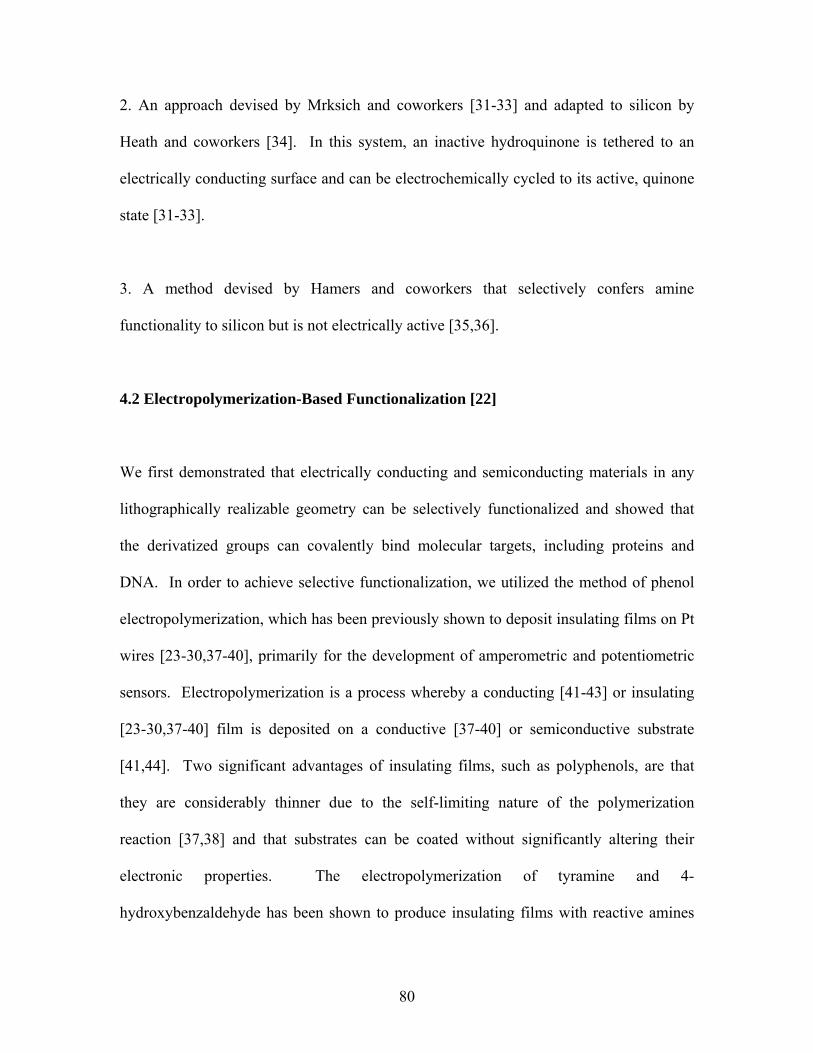
2. An approach devised by Mrksich and coworkers [31-33] and adapted to silicon by
Heath and coworkers [34]. In this system, an inactive hydroquinone is tethered to an
electrically conducting surface and can be electrochemically cycled to its active, quinone
state [31-33].
3. A method devised by Hamers and coworkers that selectively confers amine
functionality to silicon but is not electrically active [35,36].
4.2 Electropolymerization-Based Functionalization [22]
We first demonstrated that electrically conducting and semiconducting materials in any
lithographically realizable geometry can be selectively functionalized and showed that
the derivatized groups can covalently bind molecular targets, including proteins and
DNA. In order to achieve selective functionalization, we utilized the method of phenol
electropolymerization, which has been previously shown to deposit insulating films on Pt
wires [23-30,37-40], primarily for the development of amperometric and potentiometric
sensors. Electropolymerization is a process whereby a conducting [41-43] or insulating
[23-30,37-40] film is deposited on a conductive [37-40] or semiconductive substrate
[41,44]. Two significant advantages of insulating films, such as polyphenols, are that
they are considerably thinner due to the self-limiting nature of the polymerization
reaction [37,38] and that substrates can be coated without significantly altering their
electronic properties. The electropolymerization of tyramine and 4-
hydroxybenzaldehyde has been shown to produce insulating films with reactive amines
80
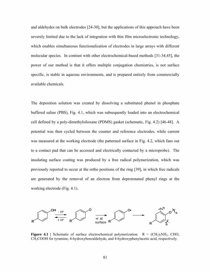
and aldehydes on bulk electrodes [24-30], but the applications of this approach have been
severely limited due to the lack of integration with thin film microelectronic technology,
which enables simultaneous functionalization of electrodes in large arrays with different
molecular species. In contrast with other electrochemical-based methods [31-34,45], the
power of our method is that it offers multiple conjugation chemistries, is not surface
specific, is stable in aqueous environments, and is prepared entirely from commercially
available chemicals.
The deposition solution was created by dissolving a substituted phenol in phosphate
buffered saline (PBS), Fig. 4.1, which was subsequently loaded into an electrochemical
cell defined by a poly-dimethylsiloxane (PDMS) gasket (schematic, Fig. 4.2) [46-48]. A
potential was then cycled between the counter and reference electrodes, while current
was measured at the working electrode (the patterned surface in Fig. 4.2, which fans out
to a contact pad that can be accessed and electrically contacted by a microprobe). The
insulating surface coating was produced by a free radical polymerization, which was
previously reported to occur at the ortho positions of the ring [39], in which free radicals
are generated by the removal of an electron from deprotonated phenyl rings at the
working electrode (Fig. 4.1).
OH
R
O
R
O
R R
O
-e- atsurface+ H+
- H+
(
(
n
n
( nOH
R
O
R
O
R R
O
-e- atsurface+ H+
- H+
(
(
n
n
( n
Figure 4.1 | Schematic of surface electrochemical polymerization. R = (CH2)2NH2, CHO, CH2COOH for tyramine, 4-hydroxybenzaldehyde, and 4-hydroxyphenylacetic acid, respectively.
81
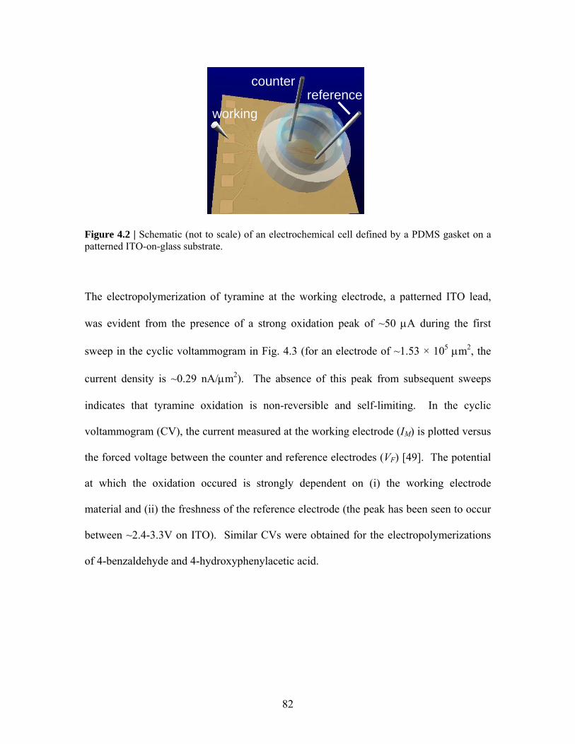
working
counterreference
working
counterreference
Figure 4.2 | Schematic (not to scale) of an electrochemical cell defined by a PDMS gasket on a patterned ITO-on-glass substrate.
The electropolymerization of tyramine at the working electrode, a patterned ITO lead,
was evident from the presence of a strong oxidation peak of ~50 μA during the first
sweep in the cyclic voltammogram in Fig. 4.3 (for an electrode of ~1.53 × 105 μm2, the
current density is ~0.29 nA/μm2). The absence of this peak from subsequent sweeps
indicates that tyramine oxidation is non-reversible and self-limiting. In the cyclic
voltammogram (CV), the current measured at the working electrode (IM) is plotted versus
the forced voltage between the counter and reference electrodes (VF) [49]. The potential
at which the oxidation occured is strongly dependent on (i) the working electrode
material and (ii) the freshness of the reference electrode (the peak has been seen to occur
between ~2.4-3.3V on ITO). Similar CVs were obtained for the electropolymerizations
of 4-benzaldehyde and 4-hydroxyphenylacetic acid.
82
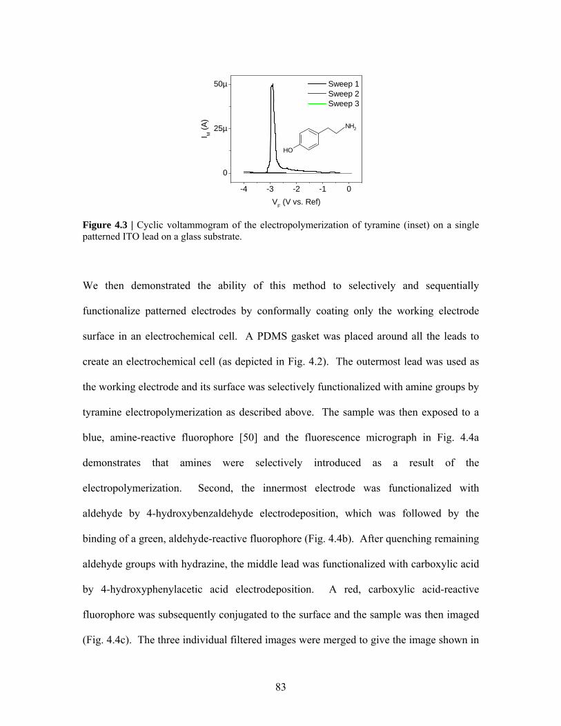
-4 -3 -2 -1 0
0
25µ
50µ
OH
NH2
I M (A
)VF (V vs. Ref)
Sweep 1 Sweep 2 Sweep 3
Figure 4.3 | Cyclic voltammogram of the electropolymerization of tyramine (inset) on a single patterned ITO lead on a glass substrate.
We then demonstrated the ability of this method to selectively and sequentially
functionalize patterned electrodes by conformally coating only the working electrode
surface in an electrochemical cell. A PDMS gasket was placed around all the leads to
create an electrochemical cell (as depicted in Fig. 4.2). The outermost lead was used as
the working electrode and its surface was selectively functionalized with amine groups by
tyramine electropolymerization as described above. The sample was then exposed to a
blue, amine-reactive fluorophore [50] and the fluorescence micrograph in Fig. 4.4a
demonstrates that amines were selectively introduced as a result of the
electropolymerization. Second, the innermost electrode was functionalized with
aldehyde by 4-hydroxybenzaldehyde electrodeposition, which was followed by the
binding of a green, aldehyde-reactive fluorophore (Fig. 4.4b). After quenching remaining
aldehyde groups with hydrazine, the middle lead was functionalized with carboxylic acid
by 4-hydroxyphenylacetic acid electrodeposition. A red, carboxylic acid-reactive
fluorophore was subsequently conjugated to the surface and the sample was then imaged
(Fig. 4.4c). The three individual filtered images were merged to give the image shown in
83
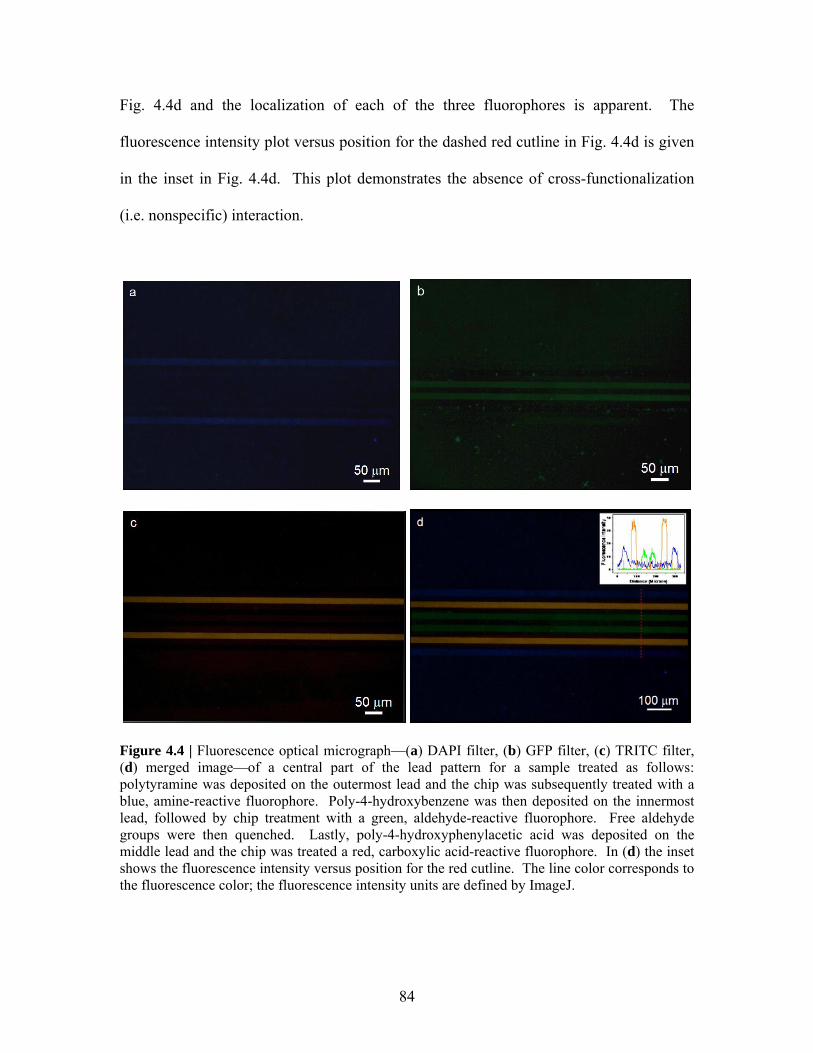
Fig. 4.4d and the localization of each of the three fluorophores is apparent. The
fluorescence intensity plot versus position for the dashed red cutline in Fig. 4.4d is given
in the inset in Fig. 4.4d. This plot demonstrates the absence of cross-functionalization
(i.e. nonspecific) interaction.
Figure 4.4 | Fluorescence optical micrograph—(a) DAPI filter, (b) GFP filter, (c) TRITC filter, (d) merged image—of a central part of the lead pattern for a sample treated as follows: polytyramine was deposited on the outermost lead and the chip was subsequently treated with a blue, amine-reactive fluorophore. Poly-4-hydroxybenzene was then deposited on the innermost lead, followed by chip treatment with a green, aldehyde-reactive fluorophore. Free aldehyde groups were then quenched. Lastly, poly-4-hydroxyphenylacetic acid was deposited on the middle lead and the chip was treated a red, carboxylic acid-reactive fluorophore. In (d) the inset shows the fluorescence intensity versus position for the red cutline. The line color corresponds to the fluorescence color; the fluorescence intensity units are defined by ImageJ.
84
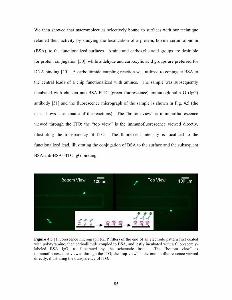
We then showed that macromolecules selectively bound to surfaces with our technique
retained their activity by studying the localization of a protein, bovine serum albumin
(BSA), to the functionalized surfaces. Amine and carboxylic acid groups are desirable
for protein conjugation [50], while aldehyde and carboxylic acid groups are preferred for
DNA binding [20]. A carbodiimide coupling reaction was utilized to conjugate BSA to
the central leads of a chip functionalized with amines. The sample was subsequently
incubated with chicken anti-BSA-FITC (green fluorescence) immunoglobulin G (IgG)
antibody [51] and the fluorescence micrograph of the sample is shown in Fig. 4.5 (the
inset shows a schematic of the reactions). The “bottom view” is immunofluorescence
viewed through the ITO; the “top view” is the immunofluorescence viewed directly,
illustrating the transparency of ITO. The fluorescent intensity is localized to the
functionalized lead, illustrating the conjugation of BSA to the surface and the subsequent
BSA-anti-BSA-FITC IgG binding.
Figure 4.5 | Fluorescence micrograph (GFP filter) of the end of an electrode pattern first coated with polytyramine, then carbodiimide coupled to BSA, and lastly incubated with a fluorescently-labeled BSA IgG, as illustrated by the schematic inset. The “bottom view” is immunofluorescence viewed through the ITO; the “top view” is the immunofluorescence viewed directly, illustrating the transparency of ITO.
85
Thus, we demonstrated that modified phenols could be electrodeposited from aqueous
solution onto lithographically patterned substrates to produce surfaces with free amine,
aldehyde, and carboxylic acid groups capable of conjugating small molecules, proteins,
and DNA oligonucelotides (see Appendix I) with no detectable cross-contamination.
Despite the utility of this approach to confer functionality to patterned electrodes, the
native oxide layer coating exposed silicon surfaces has so far prevented its application to
NBs under ambient conditions. Although only a short buffered oxide etch (BOE) is
needed to remove this native oxide coating, the subsequent washing, solution exchange,
and electrodeposition steps must occur in an inert atmosphere in order to prevent oxide
regeneration. Performing this series of sample manipulations was not possible in the
available laboratories, thus we were forced to pursue a second method for electrically-
directed functionalization. However, it is important to note that, given the proper
facilities, the electrochemical deposition approach described in this section has promise
and could potentially be applied to NB functionalization.
4.3 Electrically-Directed Silicon Functionalization [5]
We first sought to electrically direct NB functionalization by using the previously
reported hydroquinone/quinone scheme [31-34], in which an electrically active molecule
[33] is deposited and electrochemically cycled from its inactive (hydroquinone) to
reactive (quinone) state by applying a potential to the NB. This method was originally
86
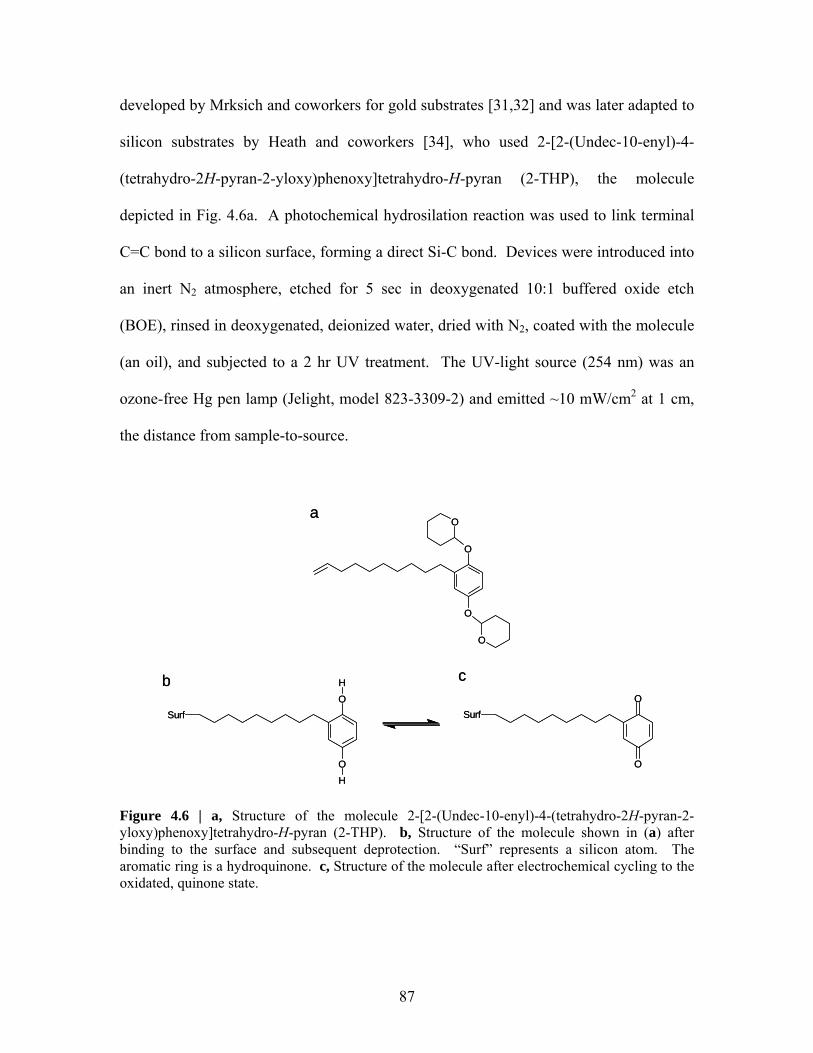
developed by Mrksich and coworkers for gold substrates [31,32] and was later adapted to
silicon substrates by Heath and coworkers [34], who used 2-[2-(Undec-10-enyl)-4-
(tetrahydro-2H-pyran-2-yloxy)phenoxy]tetrahydro-H-pyran (2-THP), the molecule
depicted in Fig. 4.6a. A photochemical hydrosilation reaction was used to link terminal
C=C bond to a silicon surface, forming a direct Si-C bond. Devices were introduced into
an inert N2 atmosphere, etched for 5 sec in deoxygenated 10:1 buffered oxide etch
(BOE), rinsed in deoxygenated, deionized water, dried with N2, coated with the molecule
(an oil), and subjected to a 2 hr UV treatment. The UV-light source (254 nm) was an
ozone-free Hg pen lamp (Jelight, model 823-3309-2) and emitted ~10 mW/cm2 at 1 cm,
the distance from sample-to-source.
SurfO
OH
H
SurfO
O
O
O
O
O
a
b c
SurfO
OH
H
SurfO
O
O
O
O
O
a
b c
Figure 4.6 | a, Structure of the molecule 2-[2-(Undec-10-enyl)-4-(tetrahydro-2H-pyran-2-yloxy)phenoxy]tetrahydro-H-pyran (2-THP). b, Structure of the molecule shown in (a) after binding to the surface and subsequent deprotection. “Surf” represents a silicon atom. The aromatic ring is a hydroquinone. c, Structure of the molecule after electrochemical cycling to the oxidated, quinone state.
87
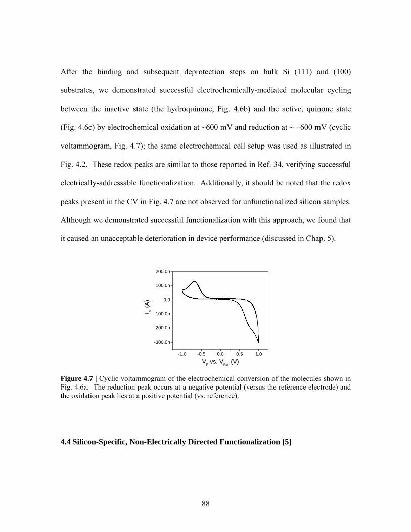
After the binding and subsequent deprotection steps on bulk Si (111) and (100)
substrates, we demonstrated successful electrochemically-mediated molecular cycling
between the inactive state (the hydroquinone, Fig. 4.6b) and the active, quinone state
(Fig. 4.6c) by electrochemical oxidation at ~600 mV and reduction at ~ –600 mV (cyclic
voltammogram, Fig. 4.7); the same electrochemical cell setup was used as illustrated in
Fig. 4.2. These redox peaks are similar to those reported in Ref. 34, verifying successful
electrically-addressable functionalization. Additionally, it should be noted that the redox
peaks present in the CV in Fig. 4.7 are not observed for unfunctionalized silicon samples.
Although we demonstrated successful functionalization with this approach, we found that
it caused an unacceptable deterioration in device performance (discussed in Chap. 5).
-1.0 -0.5 0.0 0.5 1.0
-300.0n
-200.0n
-100.0n
0.0
100.0n
200.0n
I M (A
)
VF vs. VRef (V)
Figure 4.7 | Cyclic voltammogram of the electrochemical conversion of the molecules shown in Fig. 4.6a. The reduction peak occurs at a negative potential (versus the reference electrode) and the oxidation peak lies at a positive potential (vs. reference).
4.4 Silicon-Specific, Non-Electrically Directed Functionalization [5]
88
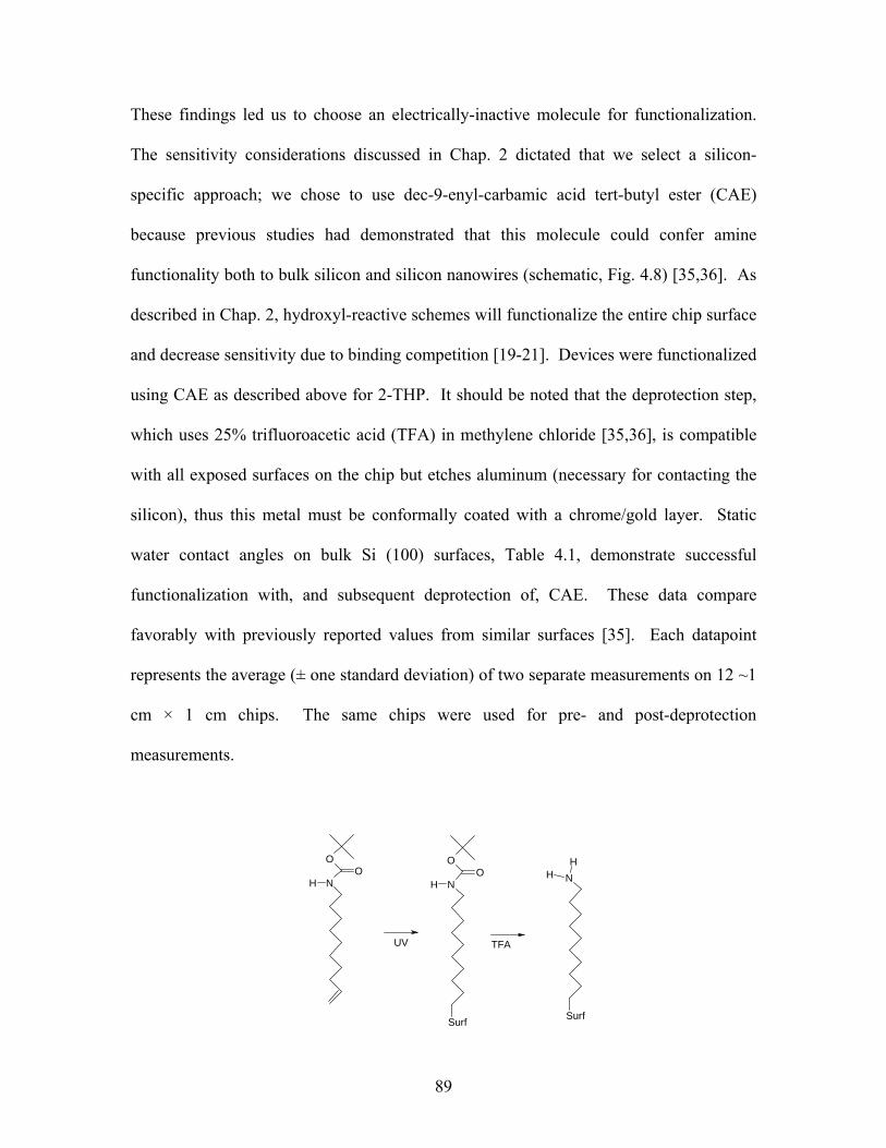
These findings led us to choose an electrically-inactive molecule for functionalization.
The sensitivity considerations discussed in Chap. 2 dictated that we select a silicon-
specific approach; we chose to use dec-9-enyl-carbamic acid tert-butyl ester (CAE)
because previous studies had demonstrated that this molecule could confer amine
functionality both to bulk silicon and silicon nanowires (schematic, Fig. 4.8) [35,36]. As
described in Chap. 2, hydroxyl-reactive schemes will functionalize the entire chip surface
and decrease sensitivity due to binding competition [19-21]. Devices were functionalized
using CAE as described above for 2-THP. It should be noted that the deprotection step,
which uses 25% trifluoroacetic acid (TFA) in methylene chloride [35,36], is compatible
with all exposed surfaces on the chip but etches aluminum (necessary for contacting the
silicon), thus this metal must be conformally coated with a chrome/gold layer. Static
water contact angles on bulk Si (100) surfaces, Table 4.1, demonstrate successful
functionalization with, and subsequent deprotection of, CAE. These data compare
favorably with previously reported values from similar surfaces [35]. Each datapoint
represents the average (± one standard deviation) of two separate measurements on 12 ~1
cm × 1 cm chips. The same chips were used for pre- and post-deprotection
measurements.
NH
OO
NH
OO
Surf
NH
Surf
H
UV TFA
89
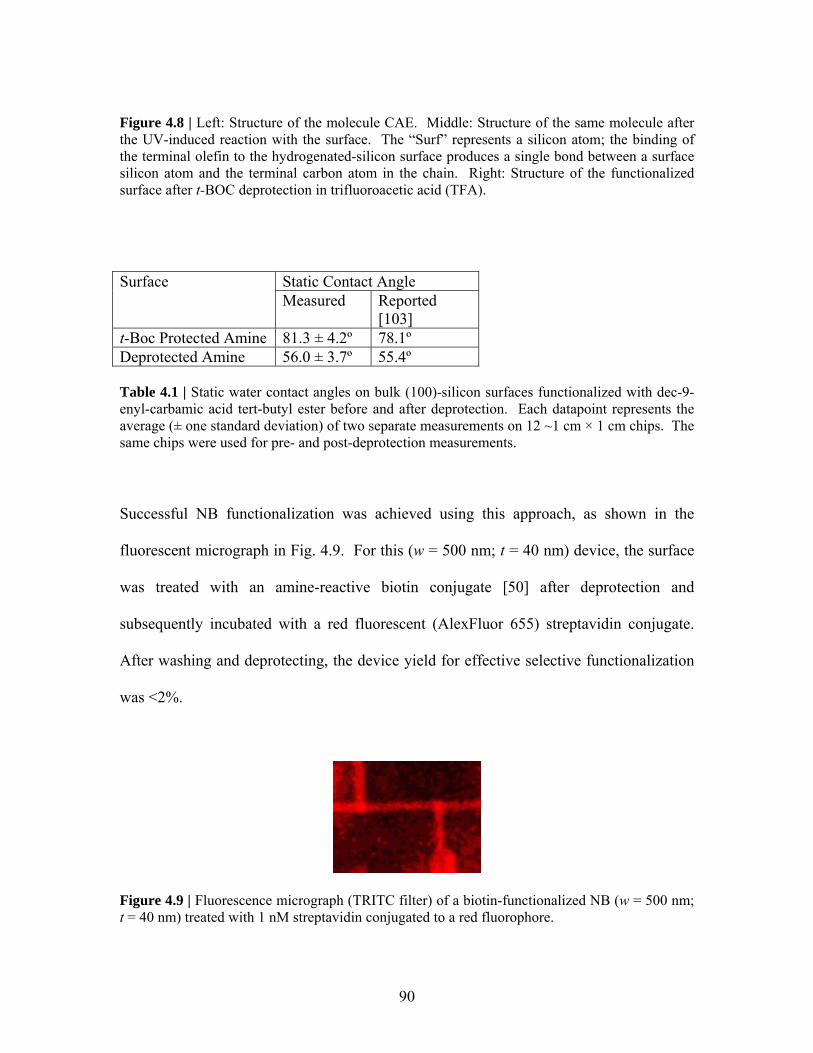
Figure 4.8 | Left: Structure of the molecule CAE. Middle: Structure of the same molecule after the UV-induced reaction with the surface. The “Surf” represents a silicon atom; the binding of the terminal olefin to the hydrogenated-silicon surface produces a single bond between a surface silicon atom and the terminal carbon atom in the chain. Right: Structure of the functionalized surface after t-BOC deprotection in trifluoroacetic acid (TFA).
Static Contact Angle Surface Measured Reported
[103]
t-Boc Protected Amine 81.3 ± 4.2º 78.1º Deprotected Amine 56.0 ± 3.7º 55.4º Table 4.1 | Static water contact angles on bulk (100)-silicon surfaces functionalized with dec-9-enyl-carbamic acid tert-butyl ester before and after deprotection. Each datapoint represents the average (± one standard deviation) of two separate measurements on 12 ~1 cm × 1 cm chips. The same chips were used for pre- and post-deprotection measurements.
Successful NB functionalization was achieved using this approach, as shown in the
fluorescent micrograph in Fig. 4.9. For this (w = 500 nm; t = 40 nm) device, the surface
was treated with an amine-reactive biotin conjugate [50] after deprotection and
subsequently incubated with a red fluorescent (AlexFluor 655) streptavidin conjugate.
After washing and deprotecting, the device yield for effective selective functionalization
was <2%.
Figure 4.9 | Fluorescence micrograph (TRITC filter) of a biotin-functionalized NB (w = 500 nm; t = 40 nm) treated with 1 nM streptavidin conjugated to a red fluorophore.
90
4.5 Non-Silicon-Specific, Non-Electrically Directed Functionalization [21]
Due to poor device yield with the CAE-functionalization approach, we used 3-
aminopropyltriethoxysilane (APTS) to functionalize devices for later studies [4,19-21].
This molecule reacts with free hydroxyls, which are abundant on oxide surfaces, and thus
converts the silanol surface to an amine surface [19-21]. In order to demonstrate
successful surface functionalization, glass slides were cut into 1” × 1” chips and were
treated with a 0.7% (v/v) solution of APTS in hexanes for 1.5 hrs at room temperature
with stirring. The chips were then washed with hexanes, toluene, and chloroform and
sonicated for 20 mins in chloroform. Next, the samples were patterned with an array of
25 μm × 25 μm squares such that the photoresist covered the entire surface except the
squares, Fig. 4.10a. The slide was then treated with an amine-reactive biotin molecule at
pH 8.4 and washed and the photoresist was subsequently removed with acetone. The
chip was next treated with an amine-reactive PEG molecule at pH 8.4 to prevent
nonspecific binding to free amines. After washing, the sample was incubated with a
green fluorescent streptavidin conjugate and was fluorescently imaged, Fig. 4.10b. The
strepavidin is seen to bind selectively to the exposed biotin surfaces, which were defined
by the photoresist pattern, verifying that the APTS approach successfully conferred
amine functionality to the substrate.
91
Figure 4.10 | a, Optical micrograph of a glass slide with photoresist patterned to expose 25 μm × 25 μm squares. b, Fluorescent micrograph (GFP filter) showing the chip in (a) after binding of green fluorescently-conjugated streptavidin.
4.6 Conclusions
We have thus demonstrated methods for conferring electrically active and inactive
chemical functionalities selectively and nonselectively to silicon surfaces. Although a
proper laboratory setup should enable the electropolymerization approach to be applied to
NBs, the sensing studies described in Chap. 5 rely solely on the photochemical
hydrosilation and the APTS approaches to selectively and nonselectively, respectively,
functionalize NB devices. Thus, through these studies we demonstrated sufficient
surface modification control to begin sensing measurements with NBs.
92
References
1. Cheng, M. M.-C. et al. Nanotechnologies for biomolecular detection and medical
diagnostics. Curr. Op. Chem. Biol. 10, 11-19 (2006).
2. Ramachandran, N., Larson, D. N., Stark, P. R. H., Hainsworth, E. & LaBaer, J.
Emerging tools for real-time label-free detection of interactions on functional
protein microarrays. FEBS J. 272, 5412-5425 (2005).
3. Klemic, J. F., Stern, E. & Reed, M. A. Hotwiring biosensors. Nature Biotech. 19,
924-925 (2001).
4. Cui, Y., Wei, Q., Park, H. & Lieber, C. M. Nanowire nanosensors for highly
sensitive and selective detection of biological and chemical species. Science 293,
1289-1292 (2001).
5. Stern, E. et al. Label-free immunodetection with CMOS-compatible
semiconducting nanowires. Nature 445, 519-522 (2007).
6. Wang, J. Carbon-nanotube based electrochemical biosensors: a review.
Electroanal. 17, 7-14 (2005).
7. Law, M., Goldberger, J. & Yang, P. D. Semiconductor nanowires and nanotubes.
Ann. Rev. Mater. Res. 34, 83-122 (2004).
8. Cheung, V. G. et al. Making and reading microarrays. Nature Genet. 21, 15-19
(1999).
9. Houseman, B. T., Huh, J. H., Kron, S. J. & Mrksich, M. Peptide chips for the
quantitative evaluation of protein kinase activity. Nature Biotech. 20, 270-274
(2002).
93
10. Blattler, T. et al. Nanopatterns with biological functions. J. Nanosci.
Nanotechnol. 6, 2237-2264 (2006).
11. Leggett, G. J. Biological nanostructures: platforms for analytical chemistry at the
sub-zeptomolar level. Analyst 130, 259-264 (2005).
12. Bernard, A., Michel, B. & Delamarche, E. Micromosaic immunoassays. Anal.
Chem. 73, 8-12 (2001).
13. LaVan, D. A., George, P. M. & Langer, R. Simple, three-dimensional
microfabrication of electrodeposited structures. Angew. Chem. Int. Ed. 42, 1262-
1265 (2003).
14. Grosjean, L. et al. A polypyrrole protein microarray for antibody-antigen
interaction studies using a label-free detection process. Anal. Biochem. 347, 193-
200 (2005).
15. Stadler, B. M., Huwiler, C. B., Voros, J. & Grandin, H. M. Light-induced in situ
patterning of DNA-tagged biomolecules and nanoparticles. IEEE Trans.
Nanobiosci. 5, 215-219 (2006).
16. Ryan, D. et al. Patterning multiple aligned self-assembled monolayers using light.
Langmuir 20, 9080-9088 (2004).
17. Rossetti, F. F., Bally, M., Michel, R., Textor, M. & Reviakine, I. Interactions
between titanium dioxide and phosphatidyl serine-containing liposomes:
formation and patterning of supported phospholipids bilayers on the surface of a
medically relevant material. Langmuir 21, 6443-6450 (2005).
18. Li, Z. et al. Sequence-specific label-free DNA sensors based on silicon
nanowires. Nano Lett. 4, 245-247 (2004).
94
19. Lindroos, K., Liljedahl, U., Raitio, M. & Syvanen, A.-C. Minisequencing on
oligonucleotide microarrays: comparison of immobilisation chemistries. Nucl.
Acid. Res. 29, Art. No. e69 (2001).
20. Taylor, S., Smith, S., Windle, B. & Guiseppi-Elie, A. Impact of surface chemistry
and blocking strategies on DNA microarrays. Nulc. Acid. Res. 31, Art. No. e87
(2003).
21. Stern, E. et al. Critical dependence of nanowire field effect transistors on Debye
screening length. Manuscript in preparation.
22. Stern, E. et al. Electropolymerization on microelectrodes: functionalization
technique for selective protein and DNA conjugation. Anal. Chem. 78, 6340-6346
(2006).
23. Adamcova, Z. & Dempirova, L. Film-forming electropolymerization. Prog. Org.
Coat. 16, 295-320 (1989).
24. Pham, M.-C., Lacaze, P.-C. & Dubois, J.-E. Obtaining thin films of “reactive
polymers” on metal surfaces by electrochemical polymerization part I. Reactivity
of functional groups in a carbonyl substituted polyphenylene oxide film. J.
Electroanal. Chem. 86, 147-157 (1978).
25. Pham, M.-C., Dubois, J.-E. & Lacaze, P.-C. Obtaining thin films of “reactive
polymers” on metal surfaces by electrochemical polymerization part II. Alcohol
substituted polyphenylene oxide films. J. Electroanal. Chem. 99, 331-340 (1979).
26. Dubois, J.-E., Lacaze, P.-C. & Pham, M. C. Obtaining thin films of “reactive
polymers” on metal surfaces by electrochemical polymerization part III. Amino-
95
substituted polyphenylene oxide films. Application to preparation of ferrocene
electroactive films. J. Electroanal. Chem. 117, 233-241 (1981).
27. Situmorang, M., Gooding, J. J., Hibbert, D. B. & Barnett, D. Electrodeposited
polytyramine as an immobilisation matrix for enzyme biosensors. Biosens.
Bioelec. 13, 953-962 (1998).
28. Situmorang, M., Gooding, J. J. & Hibbert, D. B. Immobilisation of enzyme
throughout a polytyramine matrix: a versatile procedure for fabricating
biosensors. Anal. Chim. Acta 394, 211-223 (1999).
29. Situmorang, M., Hibbert, D. B., Gooding, J. J. & Barnett, D. A sulfite biosensor
fabricated using electrodeposited polytyramine: application to wine analysis.
Analyst 124, 1775-1779 (1999).
30. Situmorang, M., Gooding, J. J., Hibbert, D. B. & Barnett, D. The development of
a pyruvate biosensor using electrodeposited polytyramine. Electroanal. 14, 17-21
(2002).
31. Yousaf, M. N. & Mrksich, M. Diels-Alder reaction for the selective
immobilization of protein to electroactive self-assembled monolayers. J. Am.
Chem. Soc. 121, 4286-4287 (1999).
32. Yeo, W.-S., Yousaf, M. N. & Mrksich, M. Dynamic interfaces between cells and
surfaces: electroactive substrates that sequentially release and attach cells. J. Am.
Chem. Soc. 125, 14994-14995 (2003).
33. Hong, H.-G. & Park, W. Electrochemical characteristics of hydroquinone-
terminated self-assembled monolayers on gold. Langmuir 17, 2485-2492 (2001).
96
34. Bunimovich, Y. L. et al. Electrochemically programmed, spatially selective
biofunctionalization of silicon wires. Langmuir 20, 10630-10638 (2004).
35. Strother, T., Hamers, R. J. & Smith, L. M. Covalent attachment of
oligodeoxyribonucleotides to amine-modified Si (001) surfaces. Nucl. Acid. Res.
28, 3535-3541 (2000).
36. Streifer, J. A., Kim, H., Nichols, B. M. & Hamers, R. J. Covalent
functionalization and biomolecular recognition properties of DNA-modified
silicon nanowires. Nanotech. 16, 1868-1873 (2005).
37. Bruno, F., Pham, M. C. & Dubois, J. E. Polaromicrotribometric study of
polyphenylene oxide film formation on metal electrodes by electrolysis of
disubstituted phenols. Electrochim. Acta 22, 451-457 (1977).
38. Eddy, S. et al. The modification of enzyme electrode properties with non-
conducting electropolymerised films. Biosens. Bioelectron. 10, 831-839 (1995).
39. Long, D. D., Marx, K. A. & Zhou, T. Amperometric hydrogen peroxide sensor
electrodes coated with electropolymerized tyrosine derivative and phenolic films.
J. Electroanal. Chem. 501, 107-113 (2001).
40. Guenbour, A., Kacemi, A. & Benbachir, A. Corrosion protection of copper by
polyaminophenol films. Prog. Org. Coat. 39, 151-155 (2000).
41. Konry, T., Novoa, A., Cosnier, S. & Marks, R. S. Development of an
“elecgtroptode” immunosensor: indium tin oxide-coated optical fiber tips
conjugated with anelectropolymerized thin film with conjugated cholera toxin B
subunit. Anal. Chem. 75, 2633-2639 (2003).
97
42. Cosnier, S. Biosensors based on electropolymerized films: new trends. Anal.
Bioanal. Chem. 377, 507-520 (2003).
43. Adamcova, Z. & Ludmila, D. Film-forming electropolymerization. Prog. Org.
Coat. 16, 295-320 (1989).
44. Moreno, J. D. et al. A galvanostatic study of the electrodeposition of polypyrrole
into porous silicon. Thin Solid Films 348, 152-156 (1999).
45. Curreli, M. et al. Selective functionalization of In2O3 nanowire mat devices for
biosensing applications. J. Am. Chem. Soc. 127, 6922-6923 (2005).
46. Duffy, D. C., McDonald, J. C., Schueller, O. J. A. & Whitesides, G. M. Rapid
prototyping of microfluidic systems in poly(dimethylsiloxane). Anal. Chem. 70,
4974-4984 (1998).
47. Li, X., Klemic, K. G., Reed, M. A. & Sigworth, F. J. Microfluidic system for
planar patch clamp electrode arrays. Nano Lett. 6, 815-819 (2006).
48. Whitesides, G. M. et al. Soft lithography in biology and biochemistry. Annu. Rev.
Biomed. Eng. 3, 335-373 (2001).
49. Bard, A. J. Electrochemical Methods – Fundamentals and Applications. 2nd Edn.
(John Wiley & Sons, New York, 2000).
50. Hermanson, G. T. Bioconjugate Techniques. (Academic Press, New York, 1996).
51. Voet, D. & Voet, J. G. Biochemistry. 2nd Edn. (John Wiley & Sons, New York,
1995).
98
Chapter 5: Nanobar Sensing
5.1 Introduction
We now discuss sensing results obtained with the devices and techniques described in the
previous chapters. We showed that the nanobars (NBs) are highly sensitive to bound
molecular charge, enabling the detection of specific label-free reagents [1-5]. Successful
sensing demonstrations with nanowire-field effect transistors (NW-FETs) had previously
been performed for ions [1], small molecules [6], proteins [7-11], DNA [12-14], and
viruses [15,16]. We began by using unfunctionalized NBs as pH sensors, enabling the
monitoring of real-time stimulus-induced cellular response without labels. Then, we
characterized functionalized devices as sensors with streptavidin and avidin and
subsequently utilized these devices to detect specific proteins and single stranded- (ss)-
DNAs.
First, the silanol-group termination of the native oxide coating of the NBs was exploited
in using the devices as hydrogen ion sensors. As discussed in Chap. 2, it has been shown
both for bulk and NW-FET devices that these silanol groups can be protonated and
deprotonated by varying solution pH, thereby gating the underlying device and
modulating the source-drain current [1-5]. We demonstrate the ability the NBs to sense
pH in a physiologically relevant range and utilize this property to measure monitor real-
time cellular response of activation-induced changes in extracellular pH [4,5].
99
Additionally, we showed that the sensitivity of a single NB device can be modulated by
accessing different transconductance regions [4].
We then utilized functionalized devices to sense specific proteins and DNA. We first
used biotinylated [3,4,17] NBs to illustrate that the NBs are sensitive to both the
magnitude and sign of adsorbed proteins (streptavidin and avidin), that complementary
detection with p- and n-type devices is possible, that the ionic strength of the solution can
be used to screen the charge, and that selectively functionalized devices can sense the
presence of <10 fM streptavidin [4,5]. We then demonstrated sensitivity to <100 fM
complementary DNA 20-mers and to <100 fM immunoglobulin G and A [4,18].
5.2 Unfunctionalized NB Sensing [4]
We begin by discussing the use of unfunctionalized NBs as hydrogen ion sensors [1-5].
The response of a large (w = 1000 nm, t = 80 nm) and small (w = 100 nm, t = 25 nm)
device to five solutions with pH varying from 6.0-8.0 (shown in blue) is displayed in Fig.
5.1. Consistent with p-type semiconducting behavior, the source-drain conduction
decreases as the acidity of the solution increases. Each device displays small hystereses
and high reproducibility (the average current levels repeat to <15%). Using the
sensitivity definition given in Eqn. (2.1), the measured sensitivity of the large NB is 10.3
and that of the small device is 43.1 for the pH range from 6.0 to 8.0.
100
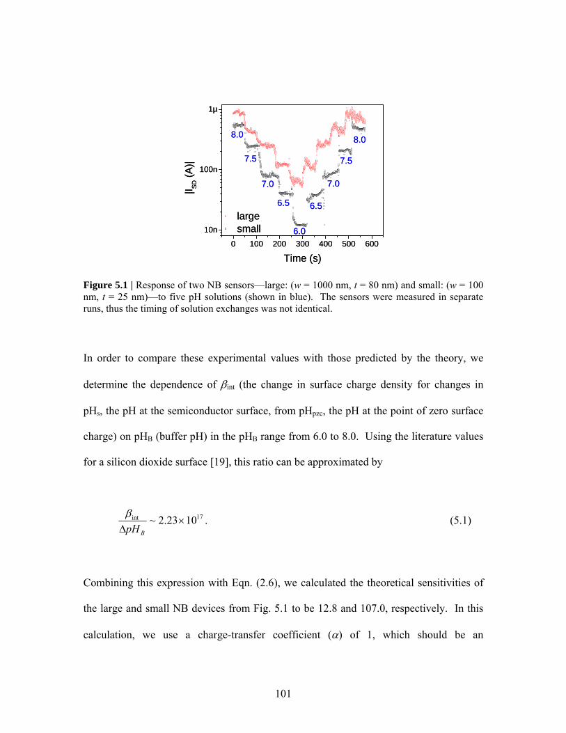
0 100 200 300 400 500 600
10n
100n
1µ
|I SD (A
)|
Time (s)
largesmall
8.0
7.5
7.0
6.5
6.0
6.5
7.0
7.5
8.0
0 100 200 300 400 500 600
10n
100n
1µ
|I SD (A
)|
Time (s)
largesmall
8.0
7.5
7.0
6.5
6.0
6.5
7.0
7.5
8.0
Figure 5.1 | Response of two NB sensors—large: (w = 1000 nm, t = 80 nm) and small: (w = 100 nm, t = 25 nm)—to five pH solutions (shown in blue). The sensors were measured in separate runs, thus the timing of solution exchanges was not identical.
In order to compare these experimental values with those predicted by the theory, we
determine the dependence of βint (the change in surface charge density for changes in
pH , the pH at the semiconductor surface, from pHs pzc, the pH at the point of zero surface
charge) on pH (buffer pH) in the pHB B range from 6.0 to 8.0. Using the literature values
for a silicon dioxide surface [19], this ratio can be approximated by
17int 1023.2~ ×Δ BpH
β . (5.1)
Combining this expression with Eqn. (2.6), we calculated the theoretical sensitivities of
the large and small NB devices from Fig. 5.1 to be 12.8 and 107.0, respectively. In this
calculation, we use a charge-transfer coefficient (α) of 1, which should be an
101
overestimate because each bound proton does not necessarily represent the loss of an
electron from the NB channel. Additionally, Eqn. (2.6) assumes a device of radius R,
only a rough approximation for the NB geometry—the NB widths are significantly
greater than their thicknesses, by 12.5- and 4-fold for the large and small devices,
repectively. In spite of these approximations, the measured sensitivities are similar to the
calculated values, indicating the NBs are functioning as nanoscale ion-sensitive FETs.
We next show the impact of device scaling on sensitivity using the devices from Fig. 5.1
as well as a third, “medium,” NB with dimensions (w = 150 nm, t = 40 nm). In Fig. 5.2,
device sensitivity [Eqn. (2.6)] for the pH range from 6.0 to 8.0 and is plotted versus the
inverse of device radius (determined as described above). As predicted in Eqn. (2.6), the
NBs scale with inverse surface area, with R2 = 0.99. The pH response from a 3 μm-wide
reative ion etch (RIE) edge-defined control structure processed simultaneously with the
NBs is also shown. This device is nominally identical with the exception of edge
definition, and illustrates RIE-induced degradation of sensing performance. The
theoretical curve is obtained as described above; the increase in predicted versus
measured sensitivities is most probably due to the choice of α, which is generally
determined experimentally [20,21], and to the inaccuracy in determining a device radius.
Although the theoretical and experimental scaling factors differ, the 1/R dependence of
the device sensitivity is clear.
102
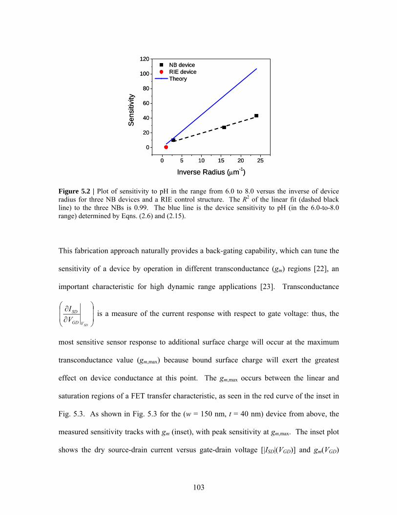
0 5 10 15 20 25
0
20
40
60
80
100
120
Sens
itivi
ty
Inverse Radius (μm-1)
NB device RIE device Theory
0 5 10 15 20 25
0
20
40
60
80
100
120
Sens
itivi
ty
Inverse Radius (μm-1)
NB device RIE device Theory
Figure 5.2 | Plot of sensitivity to pH in the range from 6.0 to 8.0 versus the inverse of device radius for three NB devices and a RIE control structure. The R2 of the linear fit (dashed black line) to the three NBs is 0.99. The blue line is the device sensitivity to pH (in the 6.0-to-8.0 range) determined by Eqns. (2.6) and (2.15).
This fabrication approach naturally provides a back-gating capability, which can tune the
sensitivity of a device by operation in different transconductance (gm) regions [22], an
important characteristic for high dynamic range applications [23]. Transconductance
⎟⎟
⎠
⎞
⎜⎜
⎝
⎛
∂∂
SDVGD
SD
VI is a measure of the current response with respect to gate voltage: thus, the
most sensitive sensor response to additional surface charge will occur at the maximum
transconductance value (gm,max) because bound surface charge will exert the greatest
effect on device conductance at this point. The gm,max occurs between the linear and
saturation regions of a FET transfer characteristic, as seen in the red curve of the inset in
Fig. 5.3. As shown in Fig. 5.3 for the (w = 150 nm, t = 40 nm) device from above, the
measured sensitivity tracks with gm (inset), with peak sensitivity at gm,max. The inset plot
shows the dry source-drain current versus gate-drain voltage [|ISD|(V )] and gGD m(V ) GD
103
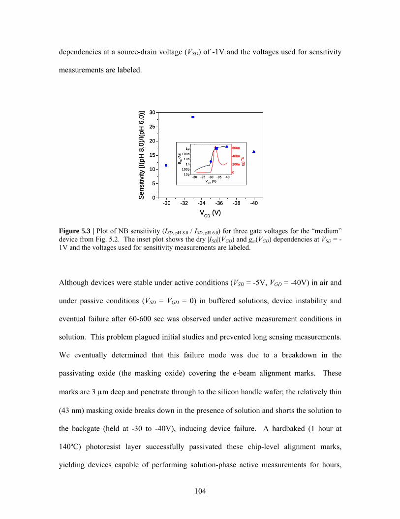
dependencies at a source-drain voltage (VSD) of -1V and the voltages used for sensitivity
measurements are labeled.
-30 -32 -34 -36 -38 -400
5
10
15
20
25
30
Sens
itivi
ty [I
(pH
8.0
)/I(p
H 6
.0)]
VGD (V)
-20 -25 -30 -35 -4010p
100p1n
10n100n
1µ
VGD (V)|I SD
(A)|
0
200n
400n
600n
gm (S)
-30 -32 -34 -36 -38 -400
5
10
15
20
25
30
Sens
itivi
ty [I
(pH
8.0
)/I(p
H 6
.0)]
VGD (V)
-20 -25 -30 -35 -4010p
100p1n
10n100n
1µ
0
200n
400n
600n
gm (S)
VGD (V)|I SD
(A)|
Figure 5.3 | Plot of NB sensitivity (ISD, pH 8.0 / ISD, pH 6.0) for three gate voltages for the “medium” device from Fig. 5.2. The inset plot shows the dry |ISD|(V ) and gGD m(V ) dependencies at VGD SD = -1V and the voltages used for sensitivity measurements are labeled.
Although devices were stable under active conditions (VSD = -5V, VGD = -40V) in air and
under passive conditions (VSD = VGD = 0) in buffered solutions, device instability and
eventual failure after 60-600 sec was observed under active measurement conditions in
solution. This problem plagued initial studies and prevented long sensing measurements.
We eventually determined that this failure mode was due to a breakdown in the
passivating oxide (the masking oxide) covering the e-beam alignment marks. These
marks are 3 μm deep and penetrate through to the silicon handle wafer; the relatively thin
(43 nm) masking oxide breaks down in the presence of solution and shorts the solution to
the backgate (held at -30 to -40V), inducing device failure. A hardbaked (1 hour at
140ºC) photoresist layer successfully passivated these chip-level alignment marks,
yielding devices capable of performing solution-phase active measurements for hours,
104
with ISD remaining within 2.7% of its initial value after an initial settling period. These
devices are subsequently referred to as “photoresist-protected” devices.
5.3 Unfunctionalized NB Sensing of Specific Cellular Responses [4,5]
To demonstrate the efficacy of these sensors in monitoring real-time cellular responses,
we analyzed the well-characterized system of T-lymphocyte activation [24]. The
development and physiology of the immune system depends, to a large degree, on the
generation and maintenance of populations of antigen-specific T-cells [25-27]. The
ability to detect functional responses arising from a small number of these cells due to
their interaction with specific ligands on a time scale of seconds may offer the potential
for rapid clinical testing, as well as high throughput epitope and drug screening [28,29].
The cellular response of antigen-specific CD8+ + or CD4 T-cells is mediated by the
interaction of the T-cell antigen receptor with peptide-loaded major histocompatability
complexes (peptide/MHC Class I or II, respectively) displayed on the surface of antigen
presenting cells [30]. Recognition of these complexes by T-cells triggers a signaling
cascade leading to activation and proliferation of effector T-cell populations. Detection
of such T-cell subsets allows monitoring of antigen-induced immunity, and is critical to
understanding the natural course and designing efficient strategies for immune
modulation and intervention [31,32]. Peptide-MHC tetramers [31,33] and dimers [32,34]
105
that bind to the T-cell receptor with high affinity have emerged as powerful tools for
enumeration of the frequency and phenotype of specific T-cells in a variety of
applications, including autoimmune disease and cancer [32,33]. However, the use of
these tools for high throughput detection and screening of rapid functional responses of
T-cell populations with different antigen specificities is limited by the lack of available
assays capable of fast and sensitive read-out from minute populations of cells.
We first used the NBs to study the antibody-mediated crosslinking of cell surface CD3,
which triggers activation of T-cells, inducing intracellular signaling and, subsequently,
engaging effector mechanisms. One consequence of such activation includes the release
of acid [35,36]. Previous studies have demonstrated extracellular acidification within
three minutes as a result of specific (peptide/MHC) [36] or non-specific (mouse-anti-
CD3ε, anti-CD3) T-cell activation [37]. As illustrated schematically in Fig. 5.4, cellular
release of protons in response to T-cell stimulation results in the protonation of the silanol
groups of the NB (active region colored black). The resulting decrease in the negative
charge on the p-type NB results in a decrease in the magnitude of the source-drain
current, |ISD|, as schematically illustrated in the |ISD| vs. time plot. The time required for T
cell activation after stimulant addition can be quantified.
106
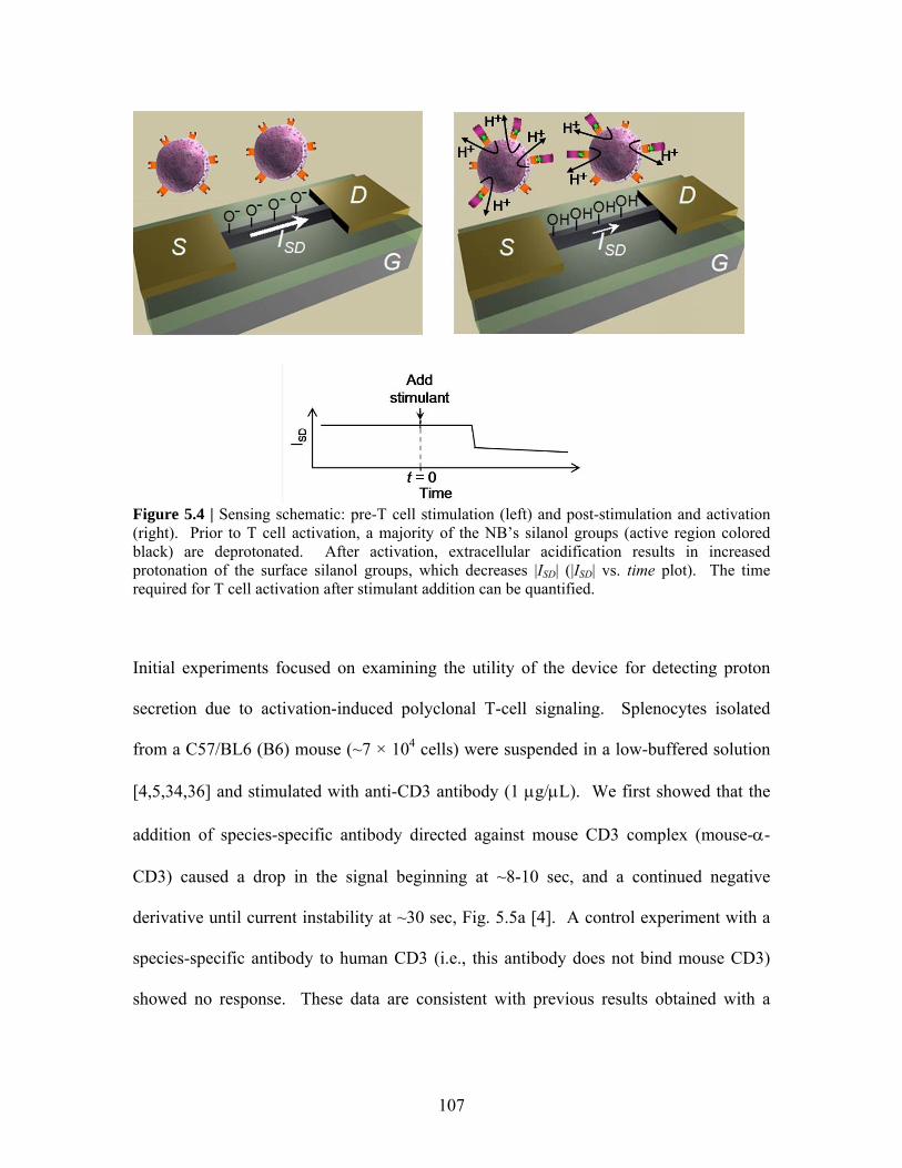
Figure 5.4 | Sensing schematic: pre-T cell stimulation (left) and post-stimulation and activation (right). Prior to T cell activation, a majority of the NB’s silanol groups (active region colored black) are deprotonated. After activation, extracellular acidification results in increased protonation of the surface silanol groups, which decreases |ISD| (|ISD| vs. time plot). The time required for T cell activation after stimulant addition can be quantified.
Initial experiments focused on examining the utility of the device for detecting proton
secretion due to activation-induced polyclonal T-cell signaling. Splenocytes isolated
from a C57/BL6 (B6) mouse (~7 × 10⁴ cells) were suspended in a low-buffered solution
[4,5,34,36] and stimulated with anti-CD3 antibody (1 μg/μL). We first showed that the
addition of species-specific antibody directed against mouse CD3 complex (mouse-α-
CD3) caused a drop in the signal beginning at ~8-10 sec, and a continued negative
derivative until current instability at ~30 sec, Fig. 5.5a [4]. A control experiment with a
species-specific antibody to human CD3 (i.e., this antibody does not bind mouse CD3)
showed no response. These data are consistent with previous results obtained with a
107
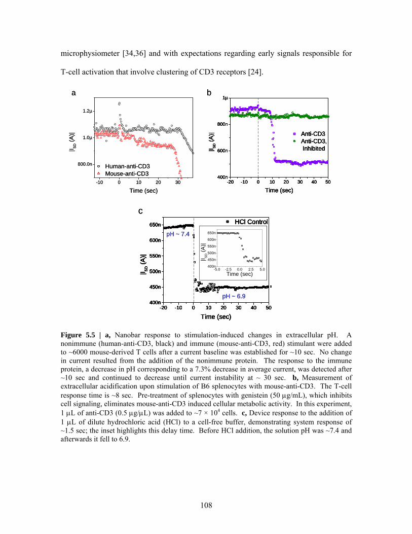
microphysiometer [34,36] and with expectations regarding early signals responsible for
T-cell activation that involve clustering of CD3 receptors [24].
-20 -10 0 10 20 30 40 50400n
600n
800n
1µ
|I SD (A
)|
Time (sec)
Anti-CD3Anti-CD3,
Inhibited
-20 -10 0 10 20 30 40 50400n
600n
800n
1µ
|I SD (A
)|
Time (sec)
Anti-CD3Anti-CD3,
Inhibited
b
-20 -10 0 10 20 30 40 50400n
600n
800n
1µ
|I SD (A
)|
Time (sec)
Anti-CD3Anti-CD3,
Inhibited
-20 -10 0 10 20 30 40 50400n
600n
800n
1µ
|I SD (A
)|
Time (sec)
Anti-CD3Anti-CD3,
Inhibited
b
-10 0 10 20 30
800.0n
1.0µ
1.2µ
|I SD (A
)|
Time (sec)
Human-anti-CD3Mouse-anti-CD3
a
-10 0 10 20 30
800.0n
1.0µ
1.2µ
|I SD (A
)|
Time (sec)
Human-anti-CD3Mouse-anti-CD3
a
-20 -10 0 10 20 30 40 50400n
450n
500n
550n
600n
650n HCl Control
|I SD (A
)|
Time (sec)
-5.0 -2.5 0.0 2.5 5.0400n
450n
500n
550n
600n
650n
|I SD (A
)|
Time (sec)
pH ~ 7.4
pH ~ 6.9
-20 -10 0 10 20 30 40 50400n
450n
500n
550n
600n
650n HCl Control
|I SD (A
)|
Time (sec)-20 -10 0 10 20 30 40 50
400n
450n
500n
550n
600n
650n HCl Control
|I SD (A
)|
Time (sec)
-5.0 -2.5 0.0 2.5 5.0400n
450n
500n
550n
600n
650n
|I SD (A
)|
Time (sec)
pH ~ 7.4
pH ~ 6.9
c
-20 -10 0 10 20 30 40 50400n
450n
500n
550n
600n
650n HCl Control
|I SD (A
)|
Time (sec)
-5.0 -2.5 0.0 2.5 5.0400n
450n
500n
550n
600n
650n
|I SD (A
)|
Time (sec)
pH ~ 7.4
pH ~ 6.9
-20 -10 0 10 20 30 40 50400n
450n
500n
550n
600n
650n HCl Control
|I SD (A
)|
Time (sec)-20 -10 0 10 20 30 40 50
400n
450n
500n
550n
600n
650n HCl Control
|I SD (A
)|
Time (sec)
-5.0 -2.5 0.0 2.5 5.0400n
450n
500n
550n
600n
650n
|I SD (A
)|
Time (sec)
pH ~ 7.4
pH ~ 6.9
c
Figure 5.5 | a, Nanobar response to stimulation-induced changes in extracellular pH. A nonimmune (human-anti-CD3, black) and immune (mouse-anti-CD3, red) stimulant were added to ~6000 mouse-derived T cells after a current baseline was established for ~10 sec. No change in current resulted from the addition of the nonimmune protein. The response to the immune protein, a decrease in pH corresponding to a 7.3% decrease in average current, was detected after ~10 sec and continued to decrease until current instability at ~ 30 sec. b, Measurement of extracellular acidification upon stimulation of B6 splenocytes with mouse-anti-CD3. The T-cell response time is ~8 sec. Pre-treatment of splenocytes with genistein (50 μg/mL), which inhibits cell signaling, eliminates mouse-anti-CD3 induced cellular metabolic activity. In this experiment, 1 μL of anti-CD3 (0.5 μg/μL) was added to ~7 × 10⁴ cells. c, Device response to the addition of 1 μL of dilute hydrochloric acid (HCl) to a cell-free buffer, demonstrating system response of ~1.5 sec; the inset highlights this delay time. Before HCl addition, the solution pH was ~7.4 and afterwards it fell to 6.9.
108
In a second experiment after the device instability was remedied, we again observed
extracellular acidification beginning within ~8-10 sec after injection of mouse-anti-CD3
(0.5 μg/μL) to B6 splenocytes, Fig. 5.5b. We determined that the system response time
to a direct change in pH was ~1.5 sec (Fig. 5.5c). Thus, the ~8-10 sec delays observed in
Fig. 5.5a and 5.5b were primarily due to the intrinsic cell response.
To ensure that extracellular pH changes were due to stimulation-induced cellular
metabolic activity, we treated splenocytes derived from the same mouse with genistein
(50 μg/mL), an antibiotic that inhibits the induced intracellular signaling cascade, without
affecting cellular viability [37]. In separate experiments, we noted that genistein, at the
concentration used in this study, did not affect cell viability as assessed by trypan-blue
staining. In the presence of genistein, addition of anti-CD3 antibody resulted in no
change in solution pH (Fig. 5.5b). This confirms that the positive response observed in
untreated cells is due to the anti-CD3 antibody-initiated proton secretion from
splenocytes, consistent with previous findings [37,38].
We next investigated the ability of this system to discriminate between well-established
peptide-specific MHC restricted responses of T-cell clones. We stimulated murine
splenocytes isolated from OT-1 and 2C transgenic mice with dimeric MHC ligands
presenting their cognate and non-cognate peptides. OT-1 and 2C CD8+ T-cells (cytotoxic
T-lymphocytes, CTLs) react well against a broad range of defined peptides presented by
a syngeneic MHC Class I, H-2Kb. OT-1 mice, expressing a transgene for the T-cell
antigen receptor, are reactive with the complex of H-2Kb and the ovalbumin octapeptide
109
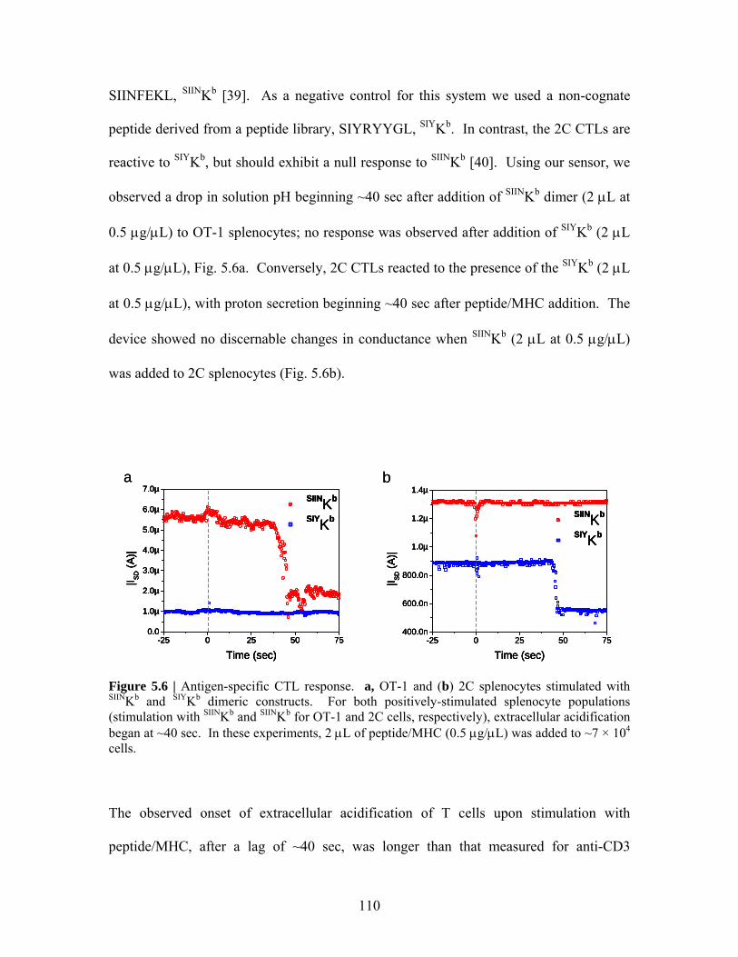
SIINSIINFEKL, Kb [39]. As a negative control for this system we used a non-cognate
peptide derived from a peptide library, SIYRYYGL, SIYKb. In contrast, the 2C CTLs are
reactive to SIYKb, but should exhibit a null response to SIINKb [40]. Using our sensor, we
observed a drop in solution pH beginning ~40 sec after addition of SIIN bK dimer (2 μL at
0.5 μg/μL) to OT-1 splenocytes; no response was observed after addition of SIYKb (2 μL
at 0.5 μg/μL), Fig. 5.6a. Conversely, 2C CTLs reacted to the presence of the SIYKb (2 μL
at 0.5 μg/μL), with proton secretion beginning ~40 sec after peptide/MHC addition. The
device showed no discernable changes in conductance when SIINKb (2 μL at 0.5 μg/μL)
was added to 2C splenocytes (Fig. 5.6b).
-25 0 25 50 750.0
1.0µ
2.0µ
3.0µ
4.0µ
5.0µ
6.0µ
7.0µ
|I SD (A
)|
Time (sec)
SIINKb
SIYKb
-25 0 25 50 750.0
1.0µ
2.0µ
3.0µ
4.0µ
5.0µ
6.0µ
7.0µ
|I SD (A
)|
Time (sec)
SIINKb
SIYKb
a
-25 0 25 50 750.0
1.0µ
2.0µ
3.0µ
4.0µ
5.0µ
6.0µ
7.0µ
|I SD (A
)|
Time (sec)
SIINKb
SIYKb
-25 0 25 50 750.0
1.0µ
2.0µ
3.0µ
4.0µ
5.0µ
6.0µ
7.0µ
|I SD (A
)|
Time (sec)
SIINKb
SIYKb
a
-25 0 25 50 75400.0n
600.0n
800.0n
1.0µ
1.2µ
1.4µ
|I SD (A
)|
Time (sec)
SIINKb
SIYKb
-25 0 25 50 75400.0n
600.0n
800.0n
1.0µ
1.2µ
1.4µ
|I SD (A
)|
Time (sec)
SIINKb
SIYKb
b
-25 0 25 50 75400.0n
600.0n
800.0n
1.0µ
1.2µ
1.4µ
|I SD (A
)|
Time (sec)
SIINKb
SIYKb
-25 0 25 50 75400.0n
600.0n
800.0n
1.0µ
1.2µ
1.4µ
|I SD (A
)|
Time (sec)
SIINKb
SIYKb
b
Figure 5.6 | Antigen-specific CTL response. a, OT-1 and (b) 2C splenocytes stimulated with SIINKb and SIYKb dimeric constructs. For both positively-stimulated splenocyte populations (stimulation with SIINKb and SIINKb for OT-1 and 2C cells, respectively), extracellular acidification began at ~40 sec. In these experiments, 2 μL of peptide/MHC (0.5 μg/μL) was added to ~7 × 10⁴ cells.
The observed onset of extracellular acidification of T cells upon stimulation with
peptide/MHC, after a lag of ~40 sec, was longer than that measured for anti-CD3
110
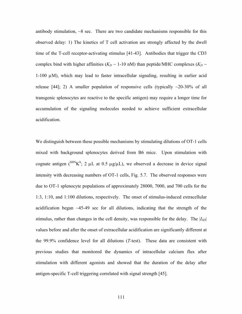
antibody stimulation, ~8 sec. There are two candidate mechanisms responsible for this
observed delay: 1) The kinetics of T cell activation are strongly affected by the dwell
time of the T-cell receptor-activating stimulus [41-43]. Antibodies that trigger the CD3
complex bind with higher affinities (KD ~ 1-10 nM) than peptide/MHC complexes (KD ~
1-100 μM), which may lead to faster intracellular signaling, resulting in earlier acid
release [44]; 2) A smaller population of responsive cells (typically ~20-30% of all
transgenic splenocytes are reactive to the specific antigen) may require a longer time for
accumulation of the signaling molecules needed to achieve sufficient extracellular
acidification.
We distinguish between these possible mechanisms by stimulating dilutions of OT-1 cells
mixed with background splenocytes derived from B6 mice. Upon stimulation with
cognate antigen (SIINKb; 2 μL at 0.5 μg/μL), we observed a decrease in device signal
intensity with decreasing numbers of OT-1 cells, Fig. 5.7. The observed responses were
due to OT-1 splenocyte populations of approximately 28000, 7000, and 700 cells for the
1:3, 1:10, and 1:100 dilutions, respectively. The onset of stimulus-induced extracellular
acidification began ~45-49 sec for all dilutions, indicating that the strength of the
stimulus, rather than changes in the cell density, was responsible for the delay. The |ISD|
values before and after the onset of extracellular acidification are significantly different at
the 99.9% confidence level for all dilutions (T-test). These data are consistent with
previous studies that monitored the dynamics of intracellular calcium flux after
stimulation with different agonists and showed that the duration of the delay after
antigen-specific T-cell triggering correlated with signal strength [45].
111
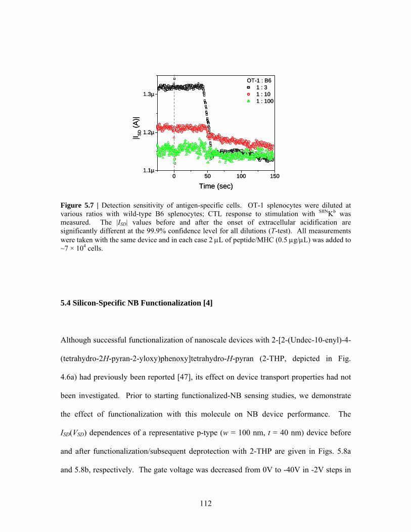
0 50 100 1501.1µ
1.2µ
1.3µ
|I SD (A
)|
Time (sec)
OT-1 : B6 1 : 3 1 : 10 1 : 100
0 50 100 1501.1µ
1.2µ
1.3µ
|I SD (A
)|
Time (sec)
OT-1 : B6 1 : 3 1 : 10 1 : 100
Figure 5.7 | Detection sensitivity of antigen-specific cells. OT-1 splenocytes were diluted at various ratios with wild-type B6 splenocytes; CTL response to stimulation with SIINKb was measured. The |ISD| values before and after the onset of extracellular acidification are significantly different at the 99.9% confidence level for all dilutions (T-test). All measurements were taken with the same device and in each case 2 μL of peptide/MHC (0.5 μg/μL) was added to ~7 × 10⁴ cells.
5.4 Silicon-Specific NB Functionalization [4]
Although successful functionalization of nanoscale devices with 2-[2-(Undec-10-enyl)-4-
(tetrahydro-2H-pyran-2-yloxy)phenoxy]tetrahydro-H-pyran (2-THP, depicted in Fig.
4.6a) had previously been reported [47], its effect on device transport properties had not
been investigated. Prior to starting functionalized-NB sensing studies, we demonstrate
the effect of functionalization with this molecule on NB device performance. The
ISD(VSD) dependences of a representative p-type (w = 100 nm, t = 40 nm) device before
and after functionalization/subsequent deprotection with 2-THP are given in Figs. 5.8a
and 5.8b, respectively. The gate voltage was decreased from 0V to -40V in -2V steps in
112
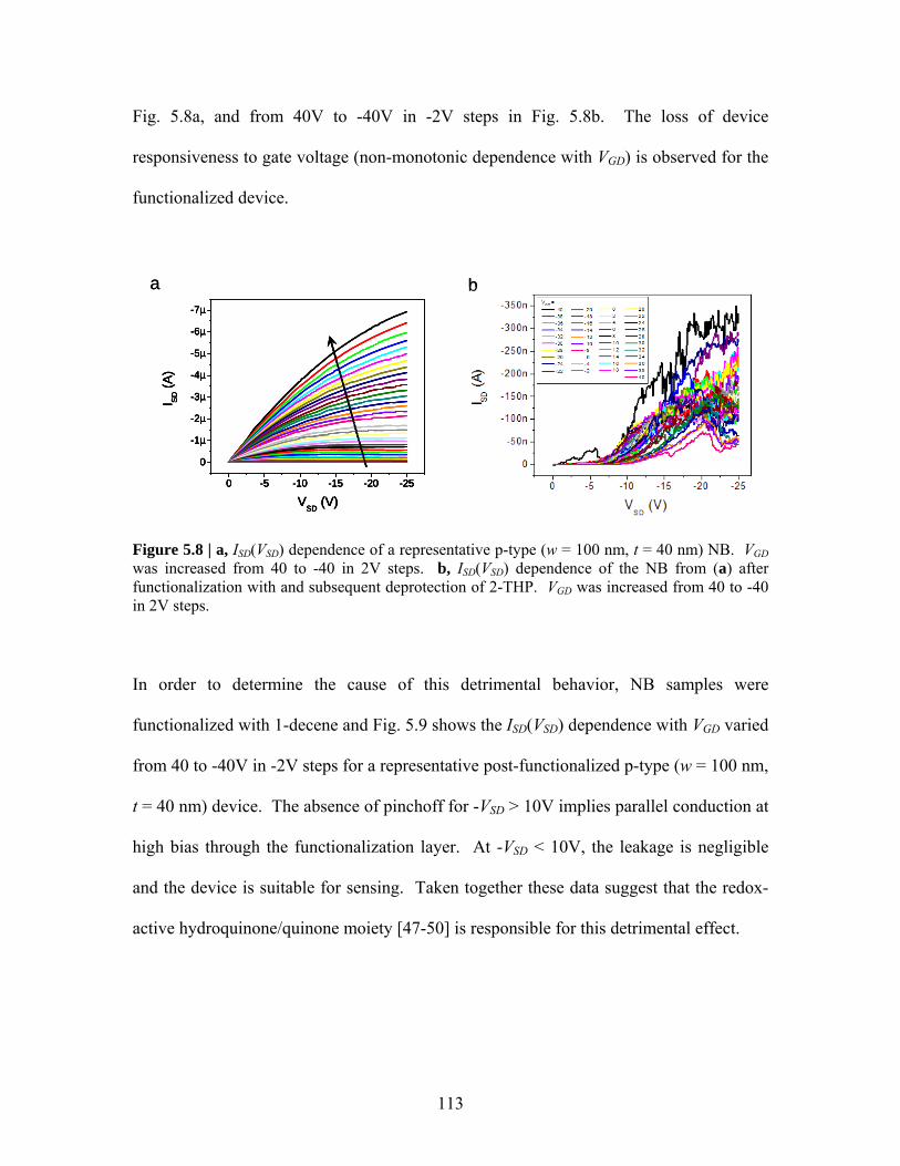
Fig. 5.8a, and from 40V to -40V in -2V steps in Fig. 5.8b. The loss of device
responsiveness to gate voltage (non-monotonic dependence with VGD) is observed for the
functionalized device.
a
0 -5 -10 -15 -20 -25
0
-1µ
-2µ
-3µ
-4µ
-5µ
-6µ
-7µ
I SD (A
)
VSD (V)0 -5 -10 -15 -20 -25
0
-1µ
-2µ
-3µ
-4µ
-5µ
-6µ
-7µ
I SD (A
)
VSD (V)
a
0 -5 -10 -15 -20 -25
0
-1µ
-2µ
-3µ
-4µ
-5µ
-6µ
-7µ
I SD (A
)
VSD (V)0 -5 -10 -15 -20 -25
0
-1µ
-2µ
-3µ
-4µ
-5µ
-6µ
-7µ
I SD (A
)
VSD (V)
bb
Figure 5.8 | a, ISD(VSD) dependence of a representative p-type (w = 100 nm, t = 40 nm) NB. VGD was increased from 40 to -40 in 2V steps. b, ISD(VSD) dependence of the NB from (a) after functionalization with and subsequent deprotection of 2-THP. VGD was increased from 40 to -40 in 2V steps.
In order to determine the cause of this detrimental behavior, NB samples were
functionalized with 1-decene and Fig. 5.9 shows the ISD(VSD) dependence with VGD varied
from 40 to -40V in -2V steps for a representative post-functionalized p-type (w = 100 nm,
t = 40 nm) device. The absence of pinchoff for -VSD > 10V implies parallel conduction at
high bias through the functionalization layer. At -VSD < 10V, the leakage is negligible
and the device is suitable for sensing. Taken together these data suggest that the redox-
active hydroquinone/quinone moiety [47-50] is responsible for this detrimental effect.
113
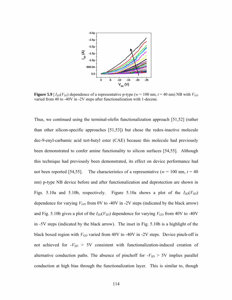
0 -5 -10 -15 -20 -25
0.0
-500.0n
-1.0µ
-1.5µ
-2.0µ
-2.5µ
-3.0µ
I SD (A
)VSD (V)
0 -5 -10 -15 -20 -25
0.0
-500.0n
-1.0µ
-1.5µ
-2.0µ
-2.5µ
-3.0µ
I SD (A
)VSD (V)
Figure 5.9 | ISD(VSD) dependence of a representative p-type (w = 100 nm, t = 40 nm) NB with VGD varied from 40 to -40V in -2V steps after functionalization with 1-decene.
Thus, we continued using the terminal-olefin functionalization approach [51,52] (rather
than other silicon-specific approaches [51,53]) but chose the redox-inactive molecule
dec-9-enyl-carbamic acid tert-butyl ester (CAE) because this molecule had previously
been demonstrated to confer amine functionality to silicon surfaces [54,55]. Although
this technique had previously been demonstrated, its effect on device performance had
not been reported [54,55]. The characteristics of a representative (w = 100 nm, t = 40
nm) p-type NB device before and after functionalization and deprotection are shown in
Figs. 5.10a and 5.10b, respectively. Figure 5.10a shows a plot of the ISD(VSD)
dependence for varying VGD from 0V to -40V in -2V steps (indicated by the black arrow)
and Fig. 5.10b gives a plot of the ISD(VSD) dependence for varying VGD from 40V to -40V
in -5V steps (indicated by the black arrow). The inset in Fig. 5.10b is a highlight of the
black boxed region with VGD varied from 40V to -40V in -2V steps. Device pinch-off is
not achieved for -VSD > 5V consistent with functionalization-induced creation of
alternative conduction paths. The absence of pinchoff for -VSD > 5V implies parallel
conduction at high bias through the functionalization layer. This is similar to, though
114
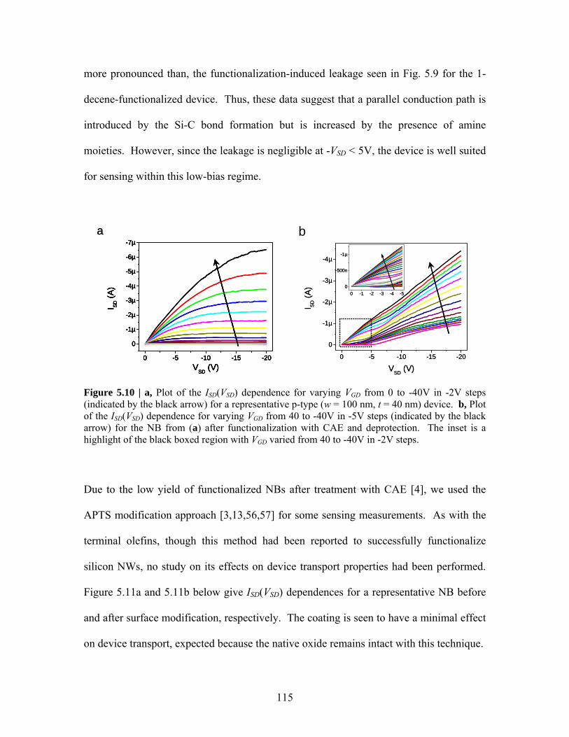
more pronounced than, the functionalization-induced leakage seen in Fig. 5.9 for the 1-
decene-functionalized device. Thus, these data suggest that a parallel conduction path is
introduced by the Si-C bond formation but is increased by the presence of amine
moieties. However, since the leakage is negligible at -VSD < 5V, the device is well suited
for sensing within this low-bias regime.
a
0 -5 -10 -15 -20
0
-1µ
-2µ
-3µ
-4µ
-5µ
-6µ
-7µ
I SD (A
)
VSD (V)0 -5 -10 -15 -20
0
-1µ
-2µ
-3µ
-4µ
-5µ
-6µ
-7µ
I SD (A
)
VSD (V)
a
0 -5 -10 -15 -20
0
-1µ
-2µ
-3µ
-4µ
-5µ
-6µ
-7µ
I SD (A
)
VSD (V)0 -5 -10 -15 -20
0
-1µ
-2µ
-3µ
-4µ
-5µ
-6µ
-7µ
I SD (A
)
VSD (V)
b
0 -5 -10 -15 -20
0
-1µ
-2µ
-3µ
-4µ
I SD (A
)
VSD (V)
0 -1 -2 -3 -4 -50
-500n
-1µ
0 -5 -10 -15 -20
0
-1µ
-2µ
-3µ
-4µ
I SD (A
)
VSD (V)
0 -1 -2 -3 -4 -50
-500n
-1µ
Figure 5.10 | a, Plot of the ISD(VSD) dependence for varying VGD from 0 to -40V in -2V steps (indicated by the black arrow) for a representative p-type (w = 100 nm, t = 40 nm) device. b, Plot of the ISD(VSD) dependence for varying VGD from 40 to -40V in -5V steps (indicated by the black arrow) for the NB from (a) after functionalization with CAE and deprotection. The inset is a highlight of the black boxed region with V varied from 40 to -40V in -2V steps. GD
Due to the low yield of functionalized NBs after treatment with CAE [4], we used the
APTS modification approach [3,13,56,57] for some sensing measurements. As with the
terminal olefins, though this method had been reported to successfully functionalize
silicon NWs, no study on its effects on device transport properties had been performed.
Figure 5.11a and 5.11b below give ISD(VSD) dependences for a representative NB before
and after surface modification, respectively. The coating is seen to have a minimal effect
on device transport, expected because the native oxide remains intact with this technique.
115
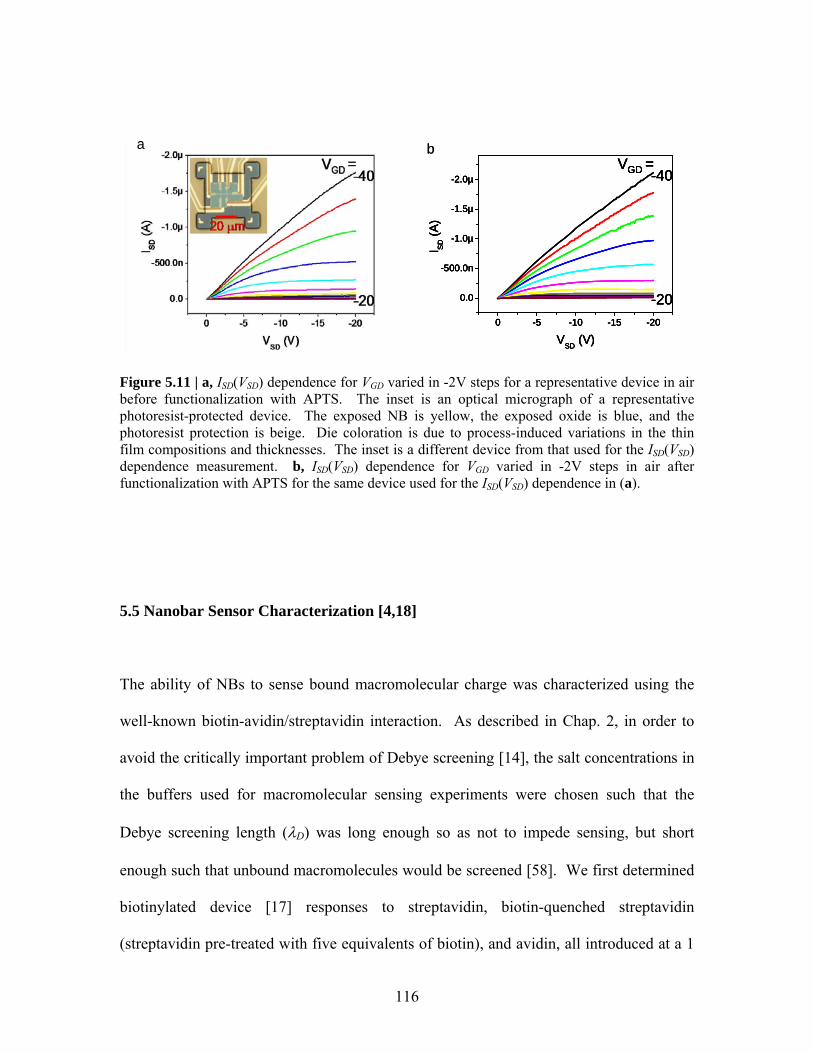
aa b
0 -5 -10 -15 -20
0.0
-500.0n
-1.0µ
-1.5µ
-2.0µ
I SD (A
)
VSD (V)
VGD =-40
-200 -5 -10 -15 -20
0.0
-500.0n
-1.0µ
-1.5µ
-2.0µ
I SD (A
)
VSD (V)
VGD =-40
-20
b
0 -5 -10 -15 -20
0.0
-500.0n
-1.0µ
-1.5µ
-2.0µ
I SD (A
)
VSD (V)
VGD =-40
-200 -5 -10 -15 -20
0.0
-500.0n
-1.0µ
-1.5µ
-2.0µ
I SD (A
)
VSD (V)
VGD =-40
-20
Figure 5.11 | a, ISD(VSD) dependence for VGD varied in -2V steps for a representative device in air before functionalization with APTS. The inset is an optical micrograph of a representative photoresist-protected device. The exposed NB is yellow, the exposed oxide is blue, and the photoresist protection is beige. Die coloration is due to process-induced variations in the thin film compositions and thicknesses. The inset is a different device from that used for the ISD(VSD) dependence measurement. b, ISD(VSD) dependence for VGD varied in -2V steps in air after functionalization with APTS for the same device used for the I ) dependence in (a). SD(VSD
5.5 Nanobar Sensor Characterization [4,18]
The ability of NBs to sense bound macromolecular charge was characterized using the
well-known biotin-avidin/streptavidin interaction. As described in Chap. 2, in order to
avoid the critically important problem of Debye screening [14], the salt concentrations in
the buffers used for macromolecular sensing experiments were chosen such that the
Debye screening length (λD) was long enough so as not to impede sensing, but short
enough such that unbound macromolecules would be screened [58]. We first determined
biotinylated device [17] responses to streptavidin, biotin-quenched streptavidin
(streptavidin pre-treated with five equivalents of biotin), and avidin, all introduced at a 1
116
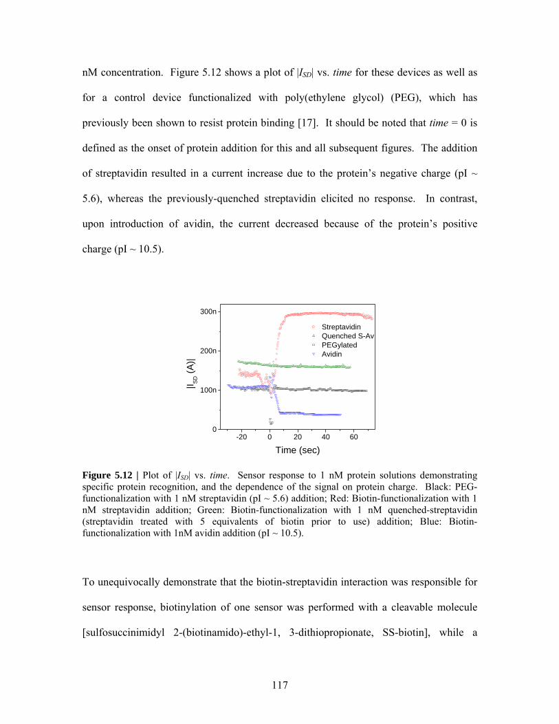
nM concentration. Figure 5.12 shows a plot of |ISD| vs. time for these devices as well as
for a control device functionalized with poly(ethylene glycol) (PEG), which has
previously been shown to resist protein binding [17]. It should be noted that time = 0 is
defined as the onset of protein addition for this and all subsequent figures. The addition
of streptavidin resulted in a current increase due to the protein’s negative charge (pI ~
5.6), whereas the previously-quenched streptavidin elicited no response. In contrast,
upon introduction of avidin, the current decreased because of the protein’s positive
charge (pI ~ 10.5).
-20 0 20 40 600
100n
200n
300n
|I SD (A
)|
Time (sec)
StreptavidinQuenched S-AvPEGylatedAvidin
Figure 5.12 | Plot of |ISD| vs. time. Sensor response to 1 nM protein solutions demonstrating specific protein recognition, and the dependence of the signal on protein charge. Black: PEG-functionalization with 1 nM streptavidin (pI ~ 5.6) addition; Red: Biotin-functionalization with 1 nM streptavidin addition; Green: Biotin-functionalization with 1 nM quenched-streptavidin (streptavidin treated with 5 equivalents of biotin prior to use) addition; Blue: Biotin-functionalization with 1nM avidin addition (pI ~ 10.5).
To unequivocally demonstrate that the biotin-streptavidin interaction was responsible for
sensor response, biotinylation of one sensor was performed with a cleavable molecule
[sulfosuccinimidyl 2-(biotinamido)-ethyl-1, 3-dithiopropionate, SS-biotin], while a
117
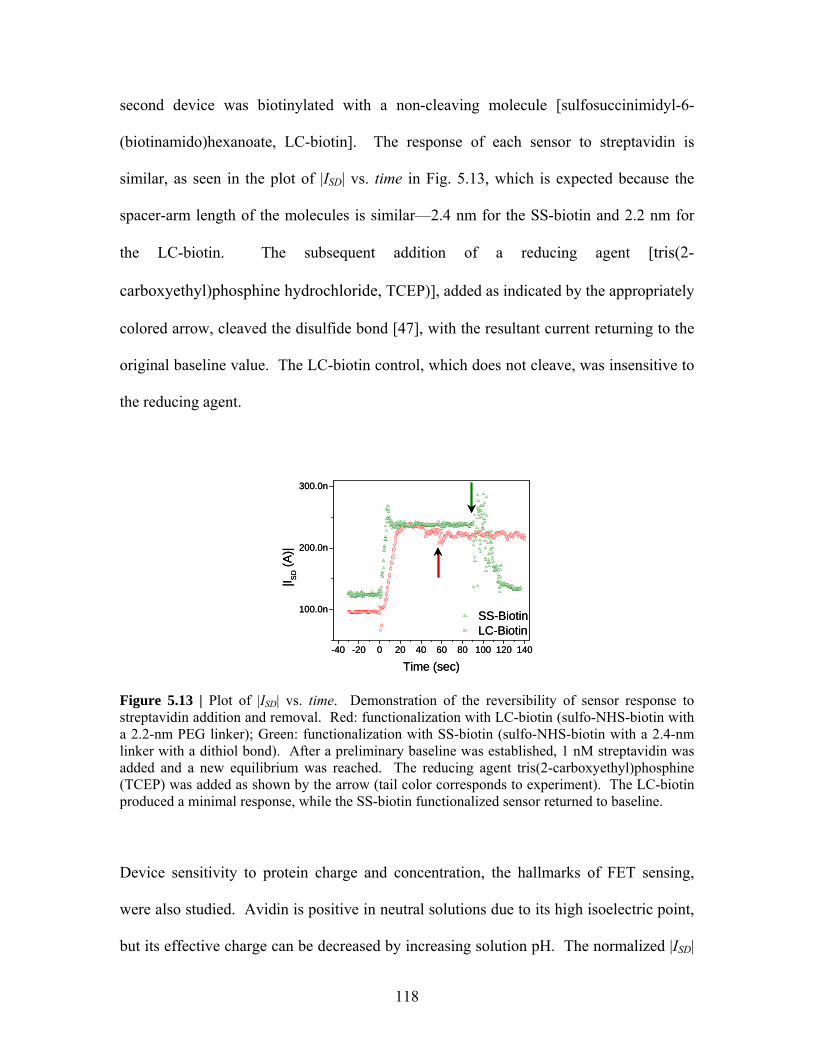
second device was biotinylated with a non-cleaving molecule [sulfosuccinimidyl-6-
(biotinamido)hexanoate, LC-biotin]. The response of each sensor to streptavidin is
similar, as seen in the plot of |ISD| vs. time in Fig. 5.13, which is expected because the
spacer-arm length of the molecules is similar—2.4 nm for the SS-biotin and 2.2 nm for
the LC-biotin. The subsequent addition of a reducing agent [tris(2-
carboxyethyl)phosphine hydrochloride, TCEP)], added as indicated by the appropriately
colored arrow, cleaved the disulfide bond [47], with the resultant current returning to the
original baseline value. The LC-biotin control, which does not cleave, was insensitive to
the reducing agent.
-40 -20 0 20 40 60 80 100 120 140
100.0n
200.0n
300.0n
|I SD (A
)|
Time (sec)
SS-BiotinLC-Biotin
-40 -20 0 20 40 60 80 100 120 140
100.0n
200.0n
300.0n
|I SD (A
)|
Time (sec)
SS-BiotinLC-Biotin
Figure 5.13 | Plot of |ISD| vs. time. Demonstration of the reversibility of sensor response to streptavidin addition and removal. Red: functionalization with LC-biotin (sulfo-NHS-biotin with a 2.2-nm PEG linker); Green: functionalization with SS-biotin (sulfo-NHS-biotin with a 2.4-nm linker with a dithiol bond). After a preliminary baseline was established, 1 nM streptavidin was added and a new equilibrium was reached. The reducing agent tris(2-carboxyethyl)phosphine (TCEP) was added as shown by the arrow (tail color corresponds to experiment). The LC-biotin produced a minimal response, while the SS-biotin functionalized sensor returned to baseline.
Device sensitivity to protein charge and concentration, the hallmarks of FET sensing,
were also studied. Avidin is positive in neutral solutions due to its high isoelectric point,
but its effective charge can be decreased by increasing solution pH. The normalized |ISD|
118
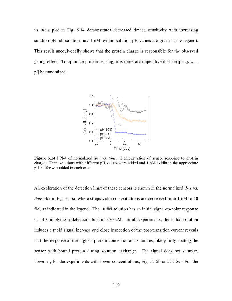
vs. time plot in Fig. 5.14 demonstrates decreased device sensitivity with increasing
solution pH (all solutions are 1 nM avidin; solution pH values are given in the legend).
This result unequivocally shows that the protein charge is responsible for the observed
gating effect. To optimize protein sensing, it is therefore imperative that the |pHsolution –
pI| be maximized.
-20 0 20 400.2
0.4
0.6
0.8
1.0
1.2
Nor
mal
ized
|ISD
|
Time (sec)
pH 10.5pH 9.0pH 7.4
Figure 5.14 | Plot of normalized |ISD| vs. time. Demonstration of sensor response to protein charge. Three solutions with different pH values were added and 1 nM avidin in the appropriate pH buffer was added in each case.
An exploration of the detection limit of these sensors is shown in the normalized |ISD| vs.
time plot in Fig. 5.15a, where streptavidin concentrations are decreased from 1 nM to 10
fM, as indicated in the legend. The 10 fM solution has an initial signal-to-noise response
of 140, implying a detection floor of ~70 aM. In all experiments, the initial solution
induces a rapid signal increase and close inspection of the post-transition current reveals
that the response at the highest protein concentrations saturates, likely fully coating the
sensor with bound protein during solution exchange. The signal does not saturate,
however, for the experiments with lower concentrations, Fig. 5.15b and 5.15c. For the
119
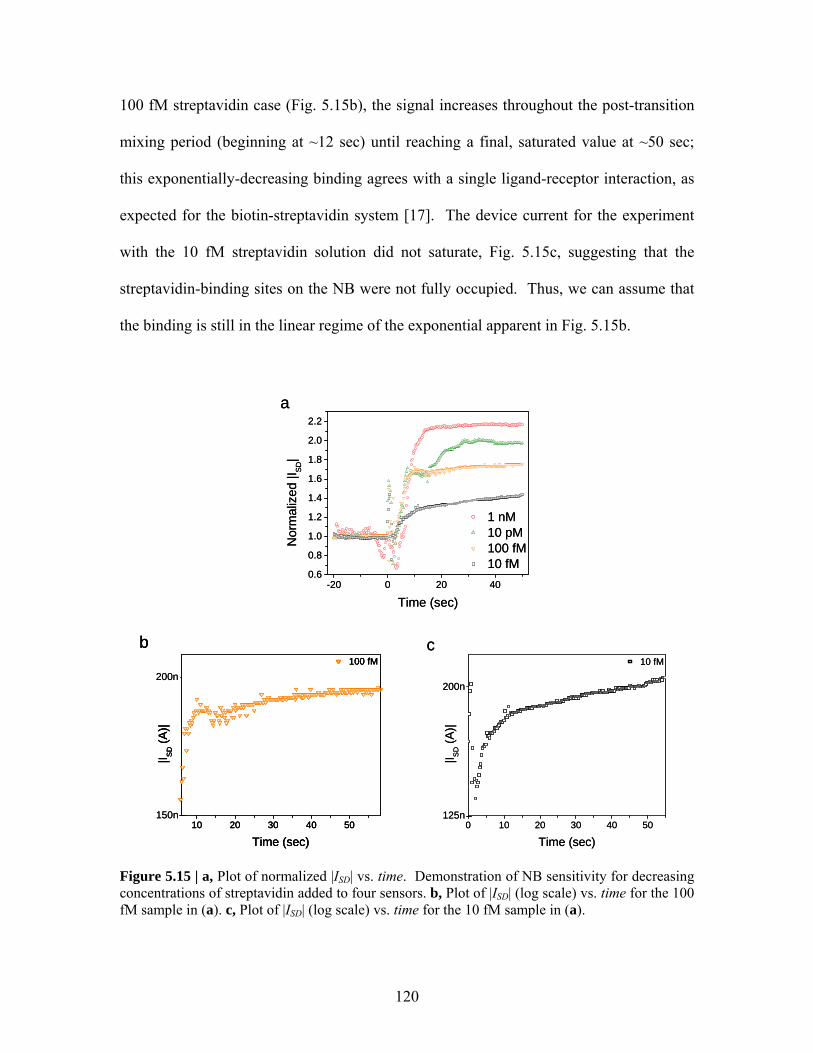
100 fM streptavidin case (Fig. 5.15b), the signal increases throughout the post-transition
mixing period (beginning at ~12 sec) until reaching a final, saturated value at ~50 sec;
this exponentially-decreasing binding agrees with a single ligand-receptor interaction, as
expected for the biotin-streptavidin system [17]. The device current for the experiment
with the 10 fM streptavidin solution did not saturate, Fig. 5.15c, suggesting that the
streptavidin-binding sites on the NB were not fully occupied. Thus, we can assume that
the binding is still in the linear regime of the exponential apparent in Fig. 5.15b.
-20 0 20 400.6
0.8
1.0
1.2
1.4
1.6
1.8
2.0
2.2
Nor
mal
ized
|ISD
|
Time (sec)
1 nM10 pM100 fM10 fM
a
-20 0 20 400.6
0.8
1.0
1.2
1.4
1.6
1.8
2.0
2.2
Nor
mal
ized
|ISD
|
Time (sec)
1 nM10 pM100 fM10 fM
a
10 20 30 40 50
|I SD (A
)|
Time (sec)
100 fM
b
200n
150n10 20 30 40 50
|I SD (A
)|
Time (sec)
100 fM
b
10 20 30 40 50
|I SD (A
)|
Time (sec)
100 fM
b
200n
150n0 10 20 30 40 50
|I SD (A
)|
Time (sec)
10 fMc
200n
125n0 10 20 30 40 50
|I SD (A
)|
Time (sec)
10 fMc
200n
125n
Figure 5.15 | a, Plot of normalized |ISD| vs. time. Demonstration of NB sensitivity for decreasing concentrations of streptavidin added to four sensors. b, Plot of |ISD| (log scale) vs. time for the 100 fM sample in (a). c, Plot of |ISD| (log scale) vs. time for the 10 fM sample in (a).
120
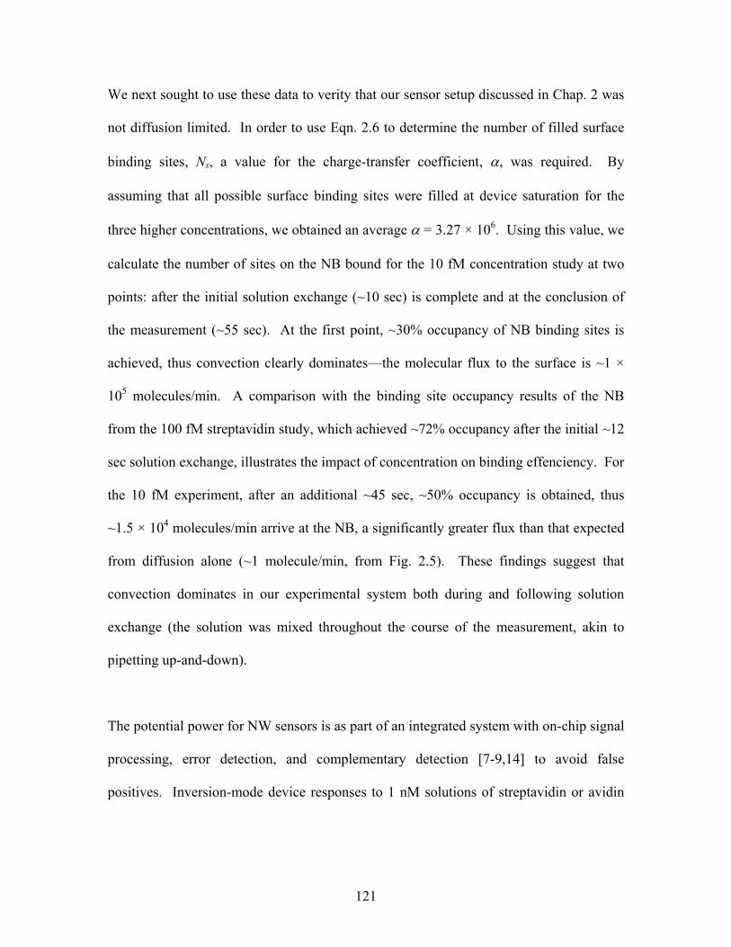
We next sought to use these data to verity that our sensor setup discussed in Chap. 2 was
not diffusion limited. In order to use Eqn. 2.6 to determine the number of filled surface
binding sites, Ns, a value for the charge-transfer coefficient, α, was required. By
assuming that all possible surface binding sites were filled at device saturation for the
three higher concentrations, we obtained an average α = 3.27 × 10⁶. Using this value, we
calculate the number of sites on the NB bound for the 10 fM concentration study at two
points: after the initial solution exchange (~10 sec) is complete and at the conclusion of
the measurement (~55 sec). At the first point, ~30% occupancy of NB binding sites is
achieved, thus convection clearly dominates—the molecular flux to the surface is ~1 ×
105 molecules/min. A comparison with the binding site occupancy results of the NB
from the 100 fM streptavidin study, which achieved ~72% occupancy after the initial ~12
sec solution exchange, illustrates the impact of concentration on binding effenciency. For
the 10 fM experiment, after an additional ~45 sec, ~50% occupancy is obtained, thus
~1.5 × 10⁴ molecules/min arrive at the NB, a significantly greater flux than that expected
from diffusion alone (~1 molecule/min, from Fig. 2.5). These findings suggest that
convection dominates in our experimental system both during and following solution
exchange (the solution was mixed throughout the course of the measurement, akin to
pipetting up-and-down).
The potential power for NW sensors is as part of an integrated system with on-chip signal
processing, error detection, and complementary detection [7-9,14] to avoid false
positives. Inversion-mode device responses to 1 nM solutions of streptavidin or avidin
121
are shown in the plot of ISD vs. time in Fig. 5.16. These devices react with the opposite
sense of the accumulation-mode devices shown previously.
-20 0 20 40
100n
200n
300n
400n
I SD (A
)
Time (sec)
AvidinStreptavidin
Figure 5.16 | Plot of ISD vs. time. Demonstration of complementary sensing, showing the response of an inversion-mode sensor to 1 nM streptavidin (red) and avidin (blue) solutions. This is the opposite response of the accumulation-mode devices in Fig. 5.12.
An understanding of the effects of Debye screening on molecular charge is crucial for
any charge-based sensor. We studied this effect by varying the salt concentration of
solutions used for a single NB sensor. Devices used for these studies were photoresist
protected and functionalized using the APTS approach and subsequently functionalized
with SS-biotin. For monovalent ions, λD is roughly inversely proportional to the square
root of the ionic concentration, thus our buffers must have low salt concentrations to
enable sensing. We used three titrations of PBS—1X, 0.1X, and 0.01X—with
corresponding Debye lengths of 0.7, 2.3, and 7.3 nm, respectively (see Table 2.1), as
illustrated schematically in Fig. 5.17.
122
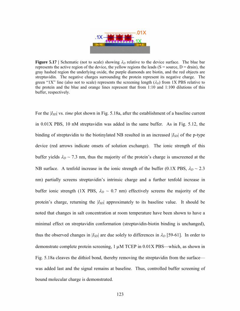
Figure 5.17 | Schematic (not to scale) showing λD relative to the device surface. The blue bar represents the active region of the device, the yellow regions the leads (S = source, D = drain), the gray hashed region the underlying oxide, the purple diamonds are biotin, and the red objects are streptavidin. The negative charges surrounding the protein represent its negative charge. The green “1X” line (also not to scale) represents the screening length (λD) from 1X PBS relative to the protein and the blue and orange lines represent that from 1:10 and 1:100 dilutions of this buffer, respectively.
For the |ISD| vs. time plot shown in Fig. 5.18a, after the establishment of a baseline current
in 0.01X PBS, 10 nM streptavidin was added in the same buffer. As in Fig. 5.12, the
binding of streptavidin to the biotinylated NB resulted in an increased |ISD| of the p-type
device (red arrows indicate onsets of solution exchange). The ionic strength of this
buffer yields λD ~ 7.3 nm, thus the majority of the protein’s charge is unscreened at the
NB surface. A tenfold increase in the ionic strength of the buffer (0.1X PBS, λD ~ 2.3
nm) partially screens streptavidin’s intrinsic charge and a further tenfold increase in
buffer ionic strength (1X PBS, λD ~ 0.7 nm) effectively screens the majority of the
protein’s charge, returning the |ISD| approximately to its baseline value. It should be
noted that changes in salt concentration at room temperature have been shown to have a
minimal effect on streptavidin conformation (streptavidin-biotin binding is unchanged),
thus the observed changes in |ISD| are due solely to differences in λD [59-61]. In order to
demonstrate complete protein screening, 1 μM TCEP in 0.01X PBS—which, as shown in
Fig. 5.18a cleaves the dithiol bond, thereby removing the streptavidin from the surface—
was added last and the signal remains at baseline. Thus, controlled buffer screening of
bound molecular charge is demonstrated.
123
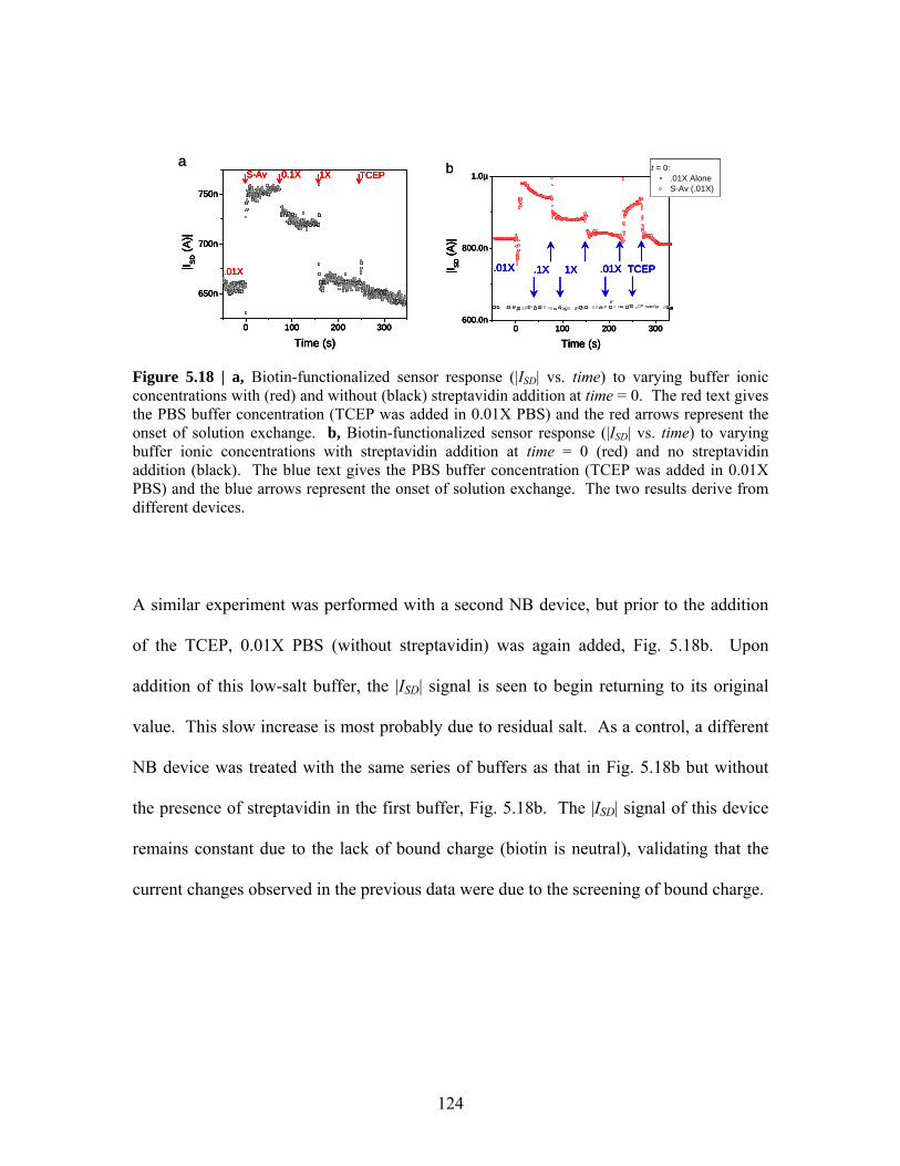
a
0 100 200 300
650n
700n
750n|I S
D (A
)|
Time (s)
0.1X 1X TCEP
.01X
S-Av
0 100 200 300
650n
700n
750n|I S
D (A
)|
Time (s)
0.1X 1X TCEP
.01X
S-Ava
0 100 200 300
650n
700n
750n
b
0 100 200 300600.0n
800.0n
1.0µ
|I SD (A
)|
Time (s)
t = 0:.01X AloneS-Av (.01X)
.1X 1X .01X TCEP.01X
0 100 200 300600.0n
800.0n
1.0µ
|I SD (A
)|
Time (s)
t = 0:.01X AloneS-Av (.01X)
.1X 1X .01X TCEP.01X
b
0 100 200 300600.0n
800.0n
1.0µ
|I SD (A
)|
Time (s)
t = 0:.01X AloneS-Av (.01X)
.1X 1X .01X TCEP.01X
0 100 200 300600.0n
800.0n
1.0µ
|I SD (A
)|
Time (s)
t = 0:.01X AloneS-Av (.01X)
.1X 1X .01X TCEP.01X|I SD (A
)|
Time (s)
0.1X 1X TCEP
.01X
S-Av
0 100 200 300
650n
700n
750n|I S
D (A
)|
Time (s)
0.1X 1X TCEP
.01X
S-Av
Figure 5.18 | a, Biotin-functionalized sensor response (|ISD| vs. time) to varying buffer ionic concentrations with (red) and without (black) streptavidin addition at time = 0. The red text gives the PBS buffer concentration (TCEP was added in 0.01X PBS) and the red arrows represent the onset of solution exchange. b, Biotin-functionalized sensor response (|ISD| vs. time) to varying buffer ionic concentrations with streptavidin addition at time = 0 (red) and no streptavidin addition (black). The blue text gives the PBS buffer concentration (TCEP was added in 0.01X PBS) and the blue arrows represent the onset of solution exchange. The two results derive from different devices.
A similar experiment was performed with a second NB device, but prior to the addition
of the TCEP, 0.01X PBS (without streptavidin) was again added, Fig. 5.18b. Upon
addition of this low-salt buffer, the |ISD| signal is seen to begin returning to its original
value. This slow increase is most probably due to residual salt. As a control, a different
NB device was treated with the same series of buffers as that in Fig. 5.18b but without
the presence of streptavidin in the first buffer, Fig. 5.18b. The |ISD| signal of this device
remains constant due to the lack of bound charge (biotin is neutral), validating that the
current changes observed in the previous data were due to the screening of bound charge.
124
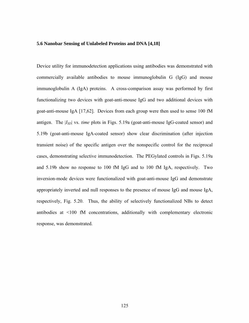
5.6 Nanobar Sensing of Unlabeled Proteins and DNA [4,18]
Device utility for immunodetection applications using antibodies was demonstrated with
commercially available antibodies to mouse immunoglobulin G (IgG) and mouse
immunoglobulin A (IgA) proteins. A cross-comparison assay was performed by first
functionalizing two devices with goat-anti-mouse IgG and two additional devices with
goat-anti-mouse IgA [17,62]. Devices from each group were then used to sense 100 fM
antigen. The |ISD| vs. time plots in Figs. 5.19a (goat-anti-mouse IgG-coated sensor) and
5.19b (goat-anti-mouse IgA-coated sensor) show clear discrimination (after injection
transient noise) of the specific antigen over the nonspecific control for the reciprocal
cases, demonstrating selective immunodetection. The PEGylated controls in Figs. 5.19a
and 5.19b show no response to 100 fM IgG and to 100 fM IgA, respectively. Two
inversion-mode devices were functionalized with goat-anti-mouse IgG and demonstrate
appropriately inverted and null responses to the presence of mouse IgG and mouse IgA,
respectively, Fig. 5.20. Thus, the ability of selectively functionalized NBs to detect
antibodies at <100 fM concentrations, additionally with complementary electronic
response, was demonstrated.
125
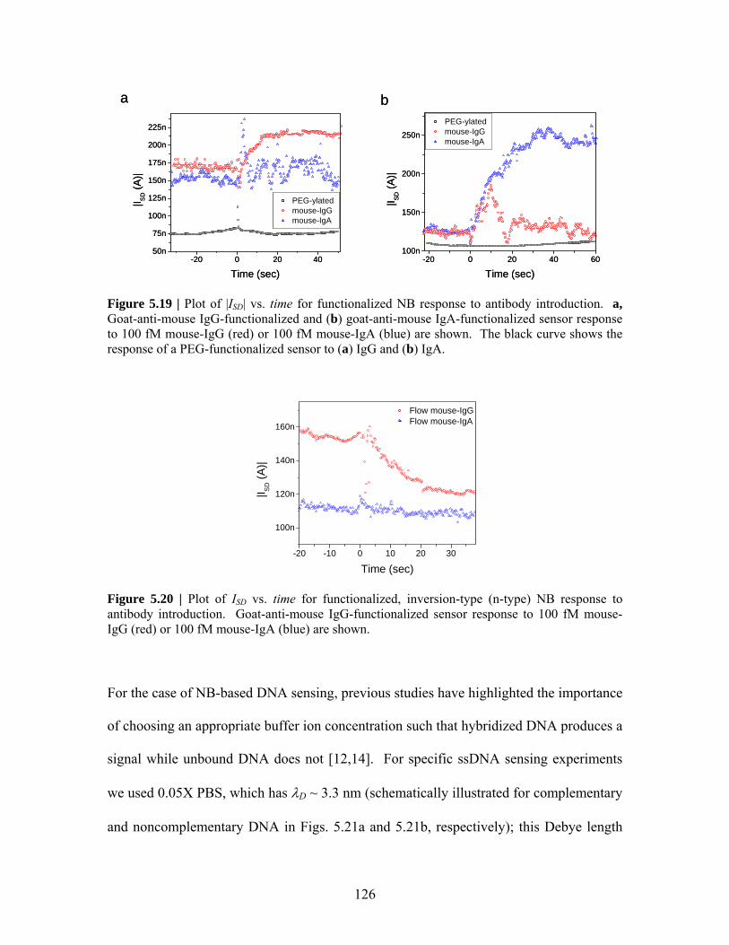
a
-20 0 20 4050n
75n
100n
125n
150n
175n
200n
225n|I S
D (A
)|
Time (sec)
PEG-ylatedmouse-IgGmouse-IgA
a
-20 0 20 4050n
75n
100n
125n
150n
175n
200n
225n|I S
D (A
)|
Time (sec)
PEG-ylatedmouse-IgGmouse-IgA
b
-20 0 20 40 60100n
150n
200n
250n
|I SD (A
)|
Time (sec)
PEG-ylatedmouse-IgGmouse-IgA
b
-20 0 20 40 60100n
150n
200n
250n
|I SD (A
)|
Time (sec)
PEG-ylatedmouse-IgGmouse-IgA
Figure 5.19 | Plot of |ISD| vs. time for functionalized NB response to antibody introduction. a, Goat-anti-mouse IgG-functionalized and (b) goat-anti-mouse IgA-functionalized sensor response to 100 fM mouse-IgG (red) or 100 fM mouse-IgA (blue) are shown. The black curve shows the response of a PEG-functionalized sensor to (a) IgG and (b) IgA.
-20 -10 0 10 20 30
100n
120n
140n
160n
|I SD (A
)|
Time (sec)
Flow mouse-IgGFlow mouse-IgA
Figure 5.20 | Plot of ISD vs. time for functionalized, inversion-type (n-type) NB response to antibody introduction. Goat-anti-mouse IgG-functionalized sensor response to 100 fM mouse-IgG (red) or 100 fM mouse-IgA (blue) are shown.
For the case of NB-based DNA sensing, previous studies have highlighted the importance
of choosing an appropriate buffer ion concentration such that hybridized DNA produces a
signal while unbound DNA does not [12,14]. For specific ssDNA sensing experiments
we used 0.05X PBS, which has λD ~ 3.3 nm (schematically illustrated for complementary
and noncomplementary DNA in Figs. 5.21a and 5.21b, respectively); this Debye length
126
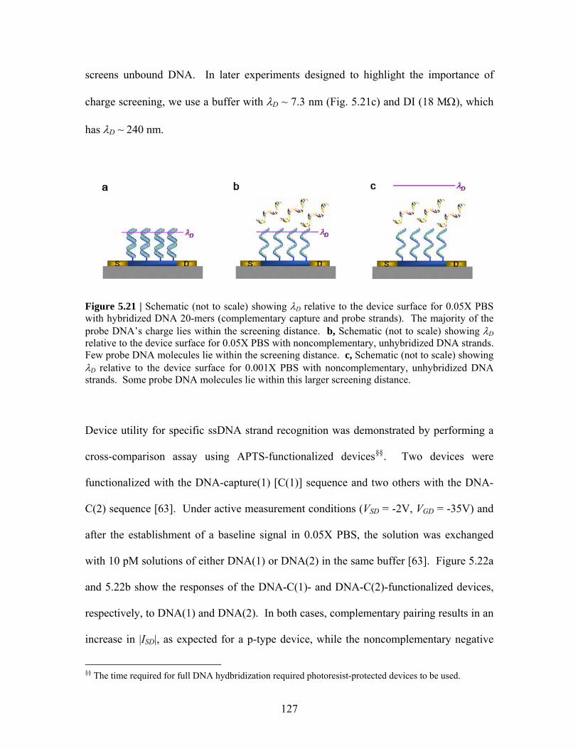
screens unbound DNA. In later experiments designed to highlight the importance of
charge screening, we use a buffer with λD ~ 7.3 nm (Fig. 5.21c) and DI (18 MΩ), which
has λD ~ 240 nm.
Figure 5.21 | Schematic (not to scale) showing λD relative to the device surface for 0.05X PBS with hybridized DNA 20-mers (complementary capture and probe strands). The majority of the probe DNA’s charge lies within the screening distance. b, Schematic (not to scale) showing λD relative to the device surface for 0.05X PBS with noncomplementary, unhybridized DNA strands. Few probe DNA molecules lie within the screening distance. c, Schematic (not to scale) showing λD relative to the device surface for 0.001X PBS with noncomplementary, unhybridized DNA strands. Some probe DNA molecules lie within this larger screening distance.
Device utility for specific ssDNA strand recognition was demonstrated by performing a
cross-comparison assay using APTS-functionalized devices§§. Two devices were
functionalized with the DNA-capture(1) [C(1)] sequence and two others with the DNA-
C(2) sequence [63]. Under active measurement conditions (VSD = -2V, VGD = -35V) and
after the establishment of a baseline signal in 0.05X PBS, the solution was exchanged
with 10 pM solutions of either DNA(1) or DNA(2) in the same buffer [63]. Figure 5.22a
and 5.22b show the responses of the DNA-C(1)- and DNA-C(2)-functionalized devices,
respectively, to DNA(1) and DNA(2). In both cases, complementary pairing results in an
increase in |ISD|, as expected for a p-type device, while the noncomplementary negative
§§ The time required for full DNA hydbridization required photoresist-protected devices to be used.
127
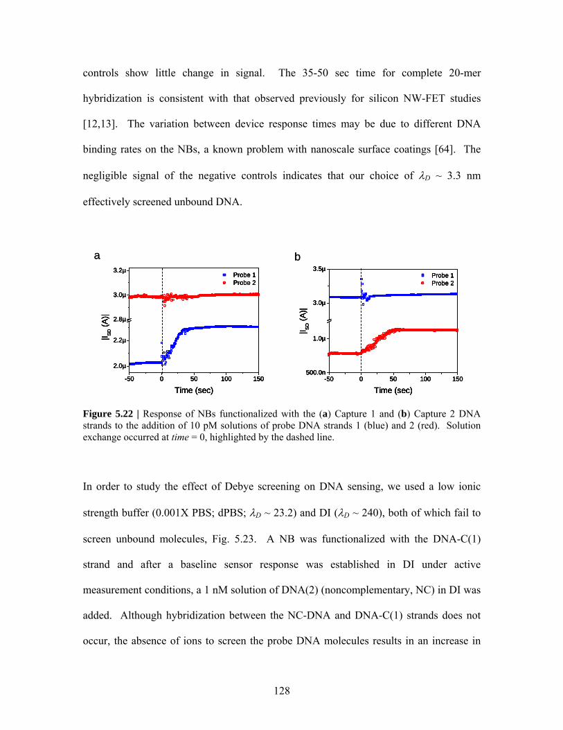
controls show little change in signal. The 35-50 sec time for complete 20-mer
hybridization is consistent with that observed previously for silicon NW-FET studies
[12,13]. The variation between device response times may be due to different DNA
binding rates on the NBs, a known problem with nanoscale surface coatings [64]. The
negligible signal of the negative controls indicates that our choice of λD ~ 3.3 nm
effectively screened unbound DNA.
a
-50 0 50 100 150
2.0µ
2.2µ
2.8µ
3.0µ
3.2µ
|I SD (A
)|
Time (sec)
Probe 1 Probe 2
-50 0 50 100 150
2.0µ
2.2µ
2.8µ
3.0µ
3.2µ
|I SD (A
)|
Time (sec)
Probe 1 Probe 2
a
-50 0 50 100 150
2.0µ
2.2µ
2.8µ
3.0µ
3.2µ
|I SD (A
)|
Time (sec)
Probe 1 Probe 2
-50 0 50 100 150
2.0µ
2.2µ
2.8µ
3.0µ
3.2µ
|I SD (A
)|
Time (sec)
Probe 1 Probe 2
b
-50 0 50 100 150500.0n
1.0µ
3.0µ
3.5µ
|I SD (A
)|
Time (sec)
Probe 1 Probe 2
-50 0 50 100 150500.0n
1.0µ
3.0µ
3.5µ
|I SD (A
)|
Time (sec)
Probe 1 Probe 2
b
-50 0 50 100 150500.0n
1.0µ
3.0µ
3.5µ
|I SD (A
)|
Time (sec)
Probe 1 Probe 2
-50 0 50 100 150500.0n
1.0µ
3.0µ
3.5µ
|I SD (A
)|
Time (sec)
Probe 1 Probe 2
Figure 5.22 | Response of NBs functionalized with the (a) Capture 1 and (b) Capture 2 DNA strands to the addition of 10 pM solutions of probe DNA strands 1 (blue) and 2 (red). Solution exchange occurred at time = 0, highlighted by the dashed line.
In order to study the effect of Debye screening on DNA sensing, we used a low ionic
strength buffer (0.001X PBS; dPBS; λD ~ 23.2) and DI (λD ~ 240), both of which fail to
screen unbound molecules, Fig. 5.23. A NB was functionalized with the DNA-C(1)
strand and after a baseline sensor response was established in DI under active
measurement conditions, a 1 nM solution of DNA(2) (noncomplementary, NC) in DI was
added. Although hybridization between the NC-DNA and DNA-C(1) strands does not
occur, the absence of ions to screen the probe DNA molecules results in an increase in
128
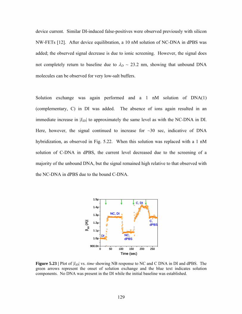
device current. Similar DI-induced false-positives were observed previously with silicon
NW-FETs [12]. After device equilibration, a 10 nM solution of NC-DNA in dPBS was
added; the observed signal decrease is due to ionic screening. However, the signal does
not completely return to baseline due to λD ~ 23.2 nm, showing that unbound DNA
molecules can be observed for very low-salt buffers.
Solution exchange was again performed and a 1 nM solution of DNA(1)
(complementary, C) in DI was added. The absence of ions again resulted in an
immediate increase in |ISD| to approximately the same level as with the NC-DNA in DI.
Here, however, the signal continued to increase for ~30 sec, indicative of DNA
hybridization, as observed in Fig. 5.22. When this solution was replaced with a 1 nM
solution of C-DNA in dPBS, the current level decreased due to the screening of a
majority of the unbound DNA, but the signal remained high relative to that observed with
the NC-DNA in dPBS due to the bound C-DNA.
0 50 100 150 200 250900.0n
1.0µ
1.1µ
1.2µ
1.3µ
1.4µ
1.5µ
|I SD (A
)|
Time (sec)
DI
NC, DI
NC,dPBS
C, DI
C,dPBS
0 50 100 150 200 250900.0n
1.0µ
1.1µ
1.2µ
1.3µ
1.4µ
1.5µ
|I SD (A
)|
Time (sec)
DI
NC, DI
NC,dPBS
C, DI
C,dPBS
Figure 5.23 | Plot of |ISD| vs. time showing NB response to NC and C DNA in DI and dPBS. The green arrows represent the onset of solution exchange and the blue text indicates solution components. No DNA was present in the DI while the initial baseline was established.
129
5.7 Conclusions
These data demonstrate that properly configured NBs can serve as pH detectors and,
when functionalized, as specific macromolecular detectors for applications that demand
ultrasensitivity with unlabeled reagents. Our cellular measurements showed that NBs can
be utilized to differentiate cell types from as few as ~210 cells, a technique that could
have powerful applications in diagnostics. Functionalized sensor measurements
demonstrated the ability of the devices to detect low concentrations of specific antibodies
(100 fM) and ssDNA (10 pM). These findings, in addition to our characterization of NB
response to Debye screening and our demonstrations of complementary sensing,
demonstrate the potential of the NBs for label-free detection of cellular response and
biomolecules.
130
References
1. Laws, G. M., Thornton, T. J., Yang, J., de la Garza, L., Kozicki, M. & Gust, D.
Molecular control of the drain current in a buried channel MOSFET. Phys. Stat.
Sol. B 233, 83-89 (2002).
2. Dzyadevych, S. V. et al. Biosensors based on enzyme field-effect transistors for
determination of some substrates and inhibitors. Anal. Bioanal. Chem. 377, 496-
506 (2003).
3. Cui, Y., Wei, Q., Park, H. & Lieber, C. M. Nanowire nanosensors for highly
sensitivie and selective detection of biological and chemical species. Science 293,
1289-1292 (2001).
4. Stern, E. et al. Label-free immunodetection with CMOS-compatible
semiconducting nanowires. Nature 445, 519-522 (2007).
5. Stern, E., Steenblock, E. R., Reed, M. A. & Fahmy, T. M. Label-free detection of
antigen-specific T cell immune responses with semiconducting nanowires.
Submitted.
6. Wang, W. U., Chen, C., Lin, K.-h., Fang, Y. & Lieber, C. M. Label-free detection
of small-molecule-protein interactions by using nanowire nanosensors. Proc. Nat.
Acad. Sci. 102, 3208-3212 (2005).
7. Tang, T. et al. Complementary response of In O2 3 nanowires and carbon nanotubes
to low-density lipoprotein chemical gating. Appl. Phys. Lett. 86, Art. No. 103903
(2005).
131
8. Li, C. et al. Complementary detection of prostate-specific antigen using In O2 3
nanowires and carbon nanotubes. J. Am. Chem. Soc. 127, 12484-12485 (2005).
9. Tang, T., Liu, X., Li, C., Lei, B., Zhang, D., Rouhanizadeh, M., Hsiai, T. & Zhou,
C. Complementary response of In O2 3 nanowires and carbon nanotubes to low-
density lipoprotein chemical gating. Appl. Phys. Lett. 86, 103903 (2005).
10. Rouhanizadeh, M., Tang, T., Li, C., Hwang, J., Zhou, C. & Hsiai, T. K.
Differentiation of oxidized low density lipoproteins by nanosensors. Sens. Act. B
114, 788-798 (2006).
11. Zheng, G., Patolsky, F., Cui. Y., Wang, W. U. & Lieber, C. M. Multiplexed
electrical detection of cancer markers with nanowire sensor arrays. Nat. Biotech.
23, 1294-1301 (2005).
12. Hahm, J.-i. & Lieber, C. M. Direct ultrasensitivie electrical detection of DNA and
DNA sequence variations using nanowire nanosensors. Nano Lett. 4, 51-54
(2004).
13. Li, Z., Chen, Y., Li, X., Kamins, T. I., Nauka, K., & Williams, R. S. Sequence-
specific label-free DNA sensors based on silicon nanowires. Nano Lett. 4, 245-
247 (2004).
14. Cheng, M. M.-C. et al. Nanotechnologies for biomolecular detection and medical
diagnostics. Curr. Op. Chem. Biol. 10, 11-19 (2006).
15. Patolsky, F., Zheng, G., Hayden, O., Lakadamyali, M., Zhuang, X. & Lieber, C.
M. Electrical detection of single viruses. Proc. Nat. Acad. Sci. 101, 14017-14022
(2004).
132
16. Patolsky, F. & Lieber, C. M. Nanowire nanosensors. Mater. Today April, 20-28
(2005).
17. Hermanson, G. T. Bioconjugate Techniques (Elsevier Science & Technology
Books, New York, 1996).
18. Stern, E. et al. Critical dependence of nanowire field effect transistors on Debye
screening length. Manuscript in preparation.
19. van Hal, R. E. G., Eijkel, J. C. T. & Bergveld, P. A novel description of ISFET
sensitivity with the buffer capacity and double-layer capacitance as key
parameters. Sens. Act. B 24-25, 201-205 (1995).
20. Fan, Z. & Lu, J. G. Gate-refreshable nanowire chemical sensors. Appl. Phys. Lett.
86, Art. No. 123510 (2005).
21. Fan, Z. & Lu, J. G. Chemical sensing with ZnO nanowire field-effect transistor.
IEEE Trans. Nanotech. 5, 393-396 (2006).
22. Sze, S. M. Physics of Semiconductor Devices 2nd Edn. (John Wiley & Sons, New
York, 1981).
23. Carrano, J. in Public Release #2435 (DARPA, 24 June 2004).
24. Trautmann, A. Microclusters initiate and sustain T cell signaling. Nature
Immmunol. 6, 1213-1214 (2005).
25. Slansky, J. E. Antigen-specific T cells: analyses of the needles in the haystack.
PLoS Biol. 1, 329-331 (2003).
26. Sallusto, F., Geginat, J. & Lanzavecchia, A. Central memory and effector memory
T cell subsets: function, generation, and maintenance. Annu. Rev. Immunol. 22,
745-763 (2004).
133
27. Lanzavecchia, A. Clonal sketches of the immune response. Embo J. 7, 2945-2951
(1998).
28. Soen, Y., Chen, D. S., Kraft, D. L., Davis, M. M. & Brown, P. O. Detection and
characterization of cellular immune responses using peptide-MHC microarrays.
PLoS Biol. 1, 429-438 (2003).
29. Chen, D. S. & Davis, M. M. Molecular and functional analysis using live cell
microarrays. Curr. Op. Chem. Biol. 10, 28-34 (2006).
30. Margulies, D. M. in Fundamental Immunology, Paul, W. E. Ed. (Lippincott-
Raven, Philadelphia, 1999), pp. 267-289.
31. Altman, J. D. et al. Phenotypic analysis of antigen-specific T lymphocytes.
Science 274, 94-96 (1996).
32. Howard, M. C., Spack, E. G., Choudhury, K., Greten, T. F. & Schneck, J. P.
MHC-based diagnostics and therapeutics-clinical applications for disease-linked
genes. Immunol. Today 20, 161-165 (1999).
33. Klenerman, P., Cerundolo, V. & Dunbar, P. R. Tracking T cells with tetramers:
new tales from new tools. Nature Rev. Immunol. 2, 263-272 (2002).
34. Crawford, F., Kozono, H., White, J., Marrack, P. & Kappler, J. Detection of
antigen-specific T cells with multivalent soluble class II MHC covalent peptide
complexes. Immunity 8, 675-682 (1998).
35. Beeson, C. et al. Early biochemical signals arise from low affinity TCR-ligand
reaction at the cell-cell interface. J. Exp. Med. 184, 777-782 (1996).
36. McConnell, H. M., Wada, H. G., Arimilli, S., Fok, K. S. & Nag, B. Stimulation of
T cells by antigen-presenting cells is kinetically controlled by antigenic peptide
134
binding to major hisocompatibility complex class II molecules. Proc. Natl. Acad.
Sci. U.S.A. 92, 2750-2754 (1995).
37. Nag, B. et al. Antigen-specific stimulation of T cell extracellular acidification by
MHC class II-peptide complexes. J. Immunol. 148, 2040-2044 (1992).
38. Owicki, J. C. et al. Continuous monitoring of receptor-mediated changes in the
metabolic rates of living cells. Proc. Natl. Acad. Sci. U.S.A. 87, 4007-4011
(1990).
39. Hogquist, K. A. et al. T cell receptor antagonist peptides induce positive
selection. Cell 76, 17-27 (1994).
40. Udaka, K. et al. Self-MHC-restricted peptides recognized by an alloreactive T
lymphocyte clone. J. Immunol. 157, 670-678 (1996).
41. Kalergis, A. M. et al. Efficient T cell activation requires an optimal dwell-time of
interaction between the TCR and the pMHC complex. Nature Immunol. 2, 229-
234 (2001).
42. Lanzavecchia, A., Iezzi, G. & Viola, A. From TCR engagement to T cell
activation: a kinetic view of T cell behavior. Cell 96, 1-4 (1999).
43. Matsui, K., Boniface, J. J., Steffner, P., Reay, P. A. & Davis, M. M. Kinetics of T-
cell receptor inding to peptide/I-Ek complexes: correlation of the dissociation rate
with T-cell reponsiveness. Proc. Natl. Acad. Sci. U.S.A. 91, 12862-12866 (1994).
44. Hennecke, J. & Wiley, D. C. T cell receptor-MHC interactions up close. Cell 104,
1-4 (2001).
45. Wulfing, C. et al. Kinetics and extent of T cell activation as measured with the
calcium signal. J. Exp. Med. 185, 1815-1825 (1997).
135
46. Wada, H. G. et al. GM-CSF triggers a rapid, glucose dependent extracellular
acidification by TF-1 cells: evidence for sodium/proton antiporter and PKC
mediated activation of acid production. J. Cell. Physiol. 154, 129-138 (1993).
47. Bunimovich, Y. L., Ge, G., Beverly, K. C., Ries, R. S., Hood, L. & Heath, J. R.
Electrochemically programmed, spatially selective biofunctionalization of silicon
wires. Langmuir 20, 10630-10638 (2004).
48. Yousaf, M. N. & Mrksich, M. Diels-Alder reaction for the selective
immobilization of protein to electroactive self-assembled monolayers. J. Am.
Chem. Soc. 121, 4286-4287 (1999).
49. Hong, H.-G. & Park, W. Electrochemical characteristics of hydroquinone-
terminated self-assembled monolayers on gold. Langmuir 17, 2485-2492 (2001).
50. Curreli, M. et al. Selective functionalization of In2O3 nanowire mat devices for
biosensing applications. J. Am. Chem. Soc. 127, 6922-6923 (2005).
51. Cicero, R. L., Linford, M. R. & Chidsey, C. E. D. Photoreactivity of unsaturated
compounds with hydrogen-terminated silicon (111). Langmuir 16, 5688-5695
(2000).
52. Sieval, A. B., Linke, R., Zuilhof, H. & Sudholter, E. J. R. High-quality alkyl
monolayers on silicon surfaces. Adv. Mater. 12, 1457-1460 (2000).
53. Mendez De Leo, L. P. & Teplyakov, A. V. Nitro group as a means of attaching
organic molecules to silicon: nitrobenzene on Si(100)-2x1. J. Phys. Chem. B 110,
6899-6905 (2006).
136
54. Streifer, J. A., Kim, H., Nichols, B.M. & Hamers, R.J. Covalent functionalization
and biomolecular recognition properties of DNA-modified silicon nanowires.
Nanotech. 16, 1868-1873 (2005).
55. Strother, T., Hamers, R. J. & Smith, L. M. Covalent attachment of
oligodeoxyribonucleotides to amine-modified Si (001) surfaces. Nucl. Acid. Res.
28, 3535-3541 (2000).
56. Lindroos, K., Liljedahl, U., Raitio, M. & Syvanen, A.-C. Minisequencing on
oligonucleotide microarrays: comparison of immobilisation chemistries. Nucl.
Acid. Res. 29, Art. No. e69 (2001).
57. Taylor, S., Smith, S., Windle, B. & Guiseppi-Elie, A. Impact of surface chemistry
and blocking strategies on DNA microarrays. Nulc. Acid. Res. 31, Art. No. e87
(2003).
58. Israelachvili, J. N. Intermolecular and Surface Forces with Applications to
Colloidal and Biological Systems. (Academic Press, New York, 1985).
59. Holmberg, A. et al. The biotin-streptavidin interaction can be reversibly broken
using water at elevated temperatures. Electrophor. 26, 501-510 (2005).
60. Savage, D. et al. Avidin-Biotin Chemistry: A Handbook. (Pierce Chemical
Company, Rockford, 1992).
61. Tong, X. & Smith, L. M. Solid-phase method for the purification of DNA
sequencing reactions. Anal. Chem. 64, 2672-2677 (1992).
62. Stern, E. et al. Electropolymerization on microelectrodes: functionalization
technique for selective protein and DNA conjugation. Anal. Chem. 78, 6340-6346
(2006).
137

63. DNA(1): 5'- CCT GCA GTG ACG CAG TGG CG -3'; DNA(2): 5'- AAG GTG
GAA AAT GTA ATC TA -3'; DNA-C(1): 5'- CGC CAC TGC GTC ACT GCA
GG -3'; DNA-C(2): 5'- TAG ATT ACA TTT TCC ACC TT -3'
64. Gupta, A. K. et al. Anomalous resonance in a nanomechanical biosensor. Proc.
Natl. Acad. Sci. U.S.A. 103, 13362-13367 (2006).
138
Chapter 6: Conclusion
We have described a novel approach to realizing fully complementary metal-oxide-
semiconductor (CMOS)-integrable silicon nanowire (NW)-like devices (nanobars, NBs)
that are capable of measuring real-time, live cellular responses and specific proteins and
DNA strands at concentrations in the femtomolar regime [1-3]. Additionally, we
demonstrated complementary sensing with n- and p-type devices and characterized
device response to molecular charge and buffer-induced ionic screening. Our work has
the potential not only to radically change clinical testing and screening but also to add
previously unheard of capabilities to assays used by basic researchers. For example, our
finding that protein sensing with NBs was dependent on the magnitude of the difference
between the solution pH and the charge-neutral or isoelectric point of the protein (pI),
|pHsolution – pI|, should enable the use a linear pH gradient to determine unknown protein
pIs, currently an extremely difficult task.
We have shown that unfunctionalized NBs are well-suited for the detection of stimulus-
induced extracellular acidification within seconds after stimulation at an unprecedented
level of sensitivity, ~210 cells (30% of 700). Though work to date has focused on one
specific cell type with variable specificities, these findings are likely to be extended to
other systems, because acid release is triggered by a general signal transduction pathway
through the generation of acidic metabolites or the activation of proton membrane
transporters [4]. The ultrasensitivity of this methodology, combined with the small
139
sample volumes required, the rapid response times observed, the suitability for high-
throughput analysis, and the ability to integrate into full electronic on-chip systems,
positions this technology for insertion into basic and clinical settings requiring detection
of antigen-specific responses. For example, the NBs could be used for rapid, inexpensive
screening of vaccine efficacy.
Throughout the work described herein, it is important to note that extensive care was paid
to theoretical considerations of functionalization, fluid exchange, and ionic screening. It
is very possible that initial reports of selective detection [5-9] may have been
misinterpreted as they did not fully consider these issues. A major finding of this thesis
was to show under what conditions true selective detection can be unambiguously
determined.
It is important to note that two significant obstacles to NB sensing currently exist. First,
device-to-device variation is still large (especially for the case of n-type, inversion-mode
devices), although this problem should be easily addressed with fabrication in an
industrial facility. Second, a high-yield method for conjugating organics selectively to
silicon surfaces, a critical requirement for specific protein and DNA sensing
measurements, has not yet been demonstrated. Although we utilized a number of
approaches in this work, each was plagued by significant shortcomings. Serious attention
must be paid to these issues in order to enable this technology to reach its full potential as
a high-density array of label-free sensors, each with specificity for a different molecule
(and, potentially, with different sensitivity thresholds).
140
Although this work focused on device and sensor performance, the strength of the
approach lies in seamless integration with CMOS technology. The ability to fabricate
NBs with a traditional parallel lithographic approach in concert with their full CMOS-
compatibility may enable the NBs to be applied to many disparate sensing environments,
from clinical diagnostics—using functionalized devices to specifically detect proteins and
DNA strands and unfunctionalized devices to screen cell types—to chemical and
biological weapons sensors—using an array of functionalized devices to screen for
airborne pathogens. In addition to their unprecedented sensitivity, the devices should
greatly decrease sample preparation costs in terms of reagents, time, and amount of
sample required, which will be greatly beneficial in both clinical and research settings.
The label-free detection mechanism should enable previously difficult field sensing of
chemicals—from screening for potential pathogens to monitoring water quality—and
through the use of chemical switches such as ribozymes [10], the NBs could be
configured to sense any molecular species of any size.
Thus, the work presented in this thesis could provide the foundation for revolutionizing
sensing across a vast number of fields. Label-free sensing, in conjunction with
microelectronic integration, should greatly decrease costs in numerous clinical, public
health, and basic research applications. Additionally, this new platform may enable
researchers to explore heretofore unobservable biomolecular properties and interactions.
141
References
1. Stern, E. et al. Label-free immunodetection with CMOS-compatible
semiconducting nanowires. Nature 445, 519-522 (2007).
2. Stern, E., Steenblock, E. R., Reed, M. A. & Fahmy, T. M. Label-free detection of
antigen-specific T cell immune responses with semiconducting nanowires.
Submitted.
3. Stern, E. et al. Critical dependence of nanowire field effect transistors on Debye
screening length. Submitted.
4. Wada, H. G. et al. GM-CSF triggers a rapid, glucose dependent extracellular
acidification by TF-1 cells: evidence for sodium/proton antiporter and PKC
mediated activation of acid production. J. Cell. Physiol. 154, 129-138 (1993).
5. Cui, Y., Wei, Q., Park, H. & Lieber, C. M. Nanowire nanosensors for highly
sensitive and selective detection of biological and chemical species. Science 293,
1281-1292 (2001).
6. Hahm, J.-i. & Lieber, C. M. Direct ultrasensitive electrical detection of DNA and
DNA sequence variations using nanowire nanosensors. Nano Lett. 4, 51-54
(2004).
7. Li, Z. et al. Sequence-specific label-free DNA sensors based on silicon
nanowires. Nano Lett. 4, 245-247 (2004).
8. Wang, W. U., Chen, C., Lin, K.-h., Fang, Y. & Lieber, C. M. Label-free detection
of small-molecule-protein interactions by using nanowires nanosensors. Proc.
Natl. Acad. Sci. U.S.A. 102, 3208-3212 (2005).
142
9. Zheng, G., Patolsky, F., Cui, Y., Wang, W. U. & Lieber, C. M. Multiplexed
electrical detection of cancer markers with nanowire sensor arrays. Nature
Biotech. 23, 1294-1301 (2005).
10. Zivarts, M., Liu, Y. & Breaker, R. R. Engineered allosteric ribozymes that
respond to specific divalent metal ions. Nucl. Acid. Res. 33, 622-631 (2005).
143
Appendix I: Functionalization Methods
AI.1 Electropolymerization Methods
Chip Patterning. For indium tin oxide (ITO) devices, positive photoresist (S1813) was
spun on ITO slides purchased from Sigma-Aldrich. The resist was patterned by contact
photolithography using a CAD Art Services transparency mask and the ITO was etched
with TE-100 tin etchant at 50ºC (Transene). For polysilicon-on-oxide samples, a doped
polysilicon deposition was performed by R. Ilic at the Cornell Nanofabrication Facility
and photoresist patterning was performed at Yale as for the ITO samples. A silicon wet
etch (126 : 50 : 1 deionized water : nitric acid : ammonium fluoride) was used to define
the structures. Chrome-on-oxide samples were fabricated with NW contacting procedure
outlined above.
Electrode Preparation. The reference electrode was fabricated by depositing AgCl on
Ag wire (Earnest Fullham, Inc) in an electrochemical cell from a saturated aqueous NaCl
solution. The counter electrode is a Pt wire (Earnest Fullham, Inc) and the working
electrode was contacted with a Cascade Microprobetip.
Electrodepositions. Tyramine, 4-hydroxybenzaldehyde, and 4-hydroxyphenylacetic acid
were purchased at the highest available grade (Sigma-Aldrich) and used without further
purification. The modified phenols were dissolved to 50mM in 1X PBS, pH = 7.4, using
144
ultrasonication; fresh solutions were made at least every hour. Electropolymerization
depositions on ITO were performed using a Gamry Femtostat by cycling the counter
electrode voltage three times from 0.1 to -4V versus the reference electrode at a sweep
rate of 100 mV/s (note that with the Gamry setup in the lab this is from -0.1 to +4V). A
comparison of depositions performed on bulk and patterned ITO shows that the peak
current during deposition scales linearly with working electrode area. Following
deposition, samples were washed with PBS and treated with this buffer with stirring for
15 minutes. Comparing depositions on bulk and patterned ITO, it is evident that the
electropolymerization peak current scales linearly with working electrode surface area.
Electrodepositions from 100mM modified-phenol in 0.1M KOH in methanol were
performed for comparison and similar results to those presented were obtained; these
solutions were used for depositions on polysilicon, silicon, and chrome. It is important to
note that nucleophilic R groups such as amines must be at least one carbon removed from
the phenyl ring, or they will also polymerize and, hence, be rendered inactive [1]. It
should also be noted that we have observed functional electropolymerized films created
from 3-hydroxybenzaldehyde and 3-hydroxyphenylacetic acid. Though not studied in
this work, ketone functionality can also be obtained by the electropolymerization of
modified phenols [2].
Silicon and Polysilicon Depositions. Successful depositions on these materials were
only achieved under inert conditions (in a N2 glovebox), directly after etching with
buffered oxide etch (BOE). It should be noted that the BOE solution must be completely
145
removed from the cell prior to electrochemical cycling because hydrofluoric acid (HF), a
component of BOE, etches silicon under such conditions.
Thickness determinations. Three thickness measurements were performed on each of
five patterned samples, in which one lead had been coated by electrodeposition. These
measurements were taken with a Tencor AlphaStep IQ surface profilometer, which was
calibrated to have ~5 nm step-height resolution. For each measurement three leads were
swept, with the coated lead located between two uncoated leads. The step-heights are
determined using the packaged software, which calculates the difference between the
average height of the lead and that of the base flanking the lead. The step-heights of the
unfunctionalized leads are averaged and the thickness of the film is then calculated by
subtracting this value from the step-height of the functionalized lead. Of the 15 total
measurements, none of which gave negative film thicknesses, four yielded film
thicknesses <5 nm, which is below the resolution of the profilometer.
Blocking measurements. The solution for blocking measurements consists of 50mM
Fe2+/Fe3+ in 0.1M KCl. The blocking measurements were performed by sweeping from -
0.5 to 0.5V versus the reference electrode at 500 mV/s ten times; the tenth curve for each
measurement is plotted.
Sample washing. Prior to all conjugation reactions, chips were rinsed three times with
1X PBS and treated with this buffer for 15 min with agitation. Before imaging, each chip
146
was rinsed with deionized water and blown dry with nitrogen gas. It should be noted that
this drying procedure displaces the glass chips that fluoresce due to nonspecific binding.
Amine fluorescence conjugation. Samples were reacted with fluorophores (Molecular
Probes) at 0.25 mg/mL in a pH=8.5 bicarbonate buffer at room temperature for 1 hr with
agitation. The red fluorophore is AlexaFluor 568 succinimidyl ester and the blue is
AlexaFluor 350 succinimidyl ester.
Aldehyde and carboxylic acid fluorescence conjugation. Samples were reacted with
fluorophores at 0.25 mg/mL in a pH=5.5 acetate buffer for 1 hr at room temperature with
agitation. The fluorophore used to bind aldehyde was AlexaFluor 488 hydrazide, sodium
salt, and that used to bind carboxylic acid was AlexaFluor 568 hydrazide, sodium salt.
The amine-coated slide used as a positive control was purchased from BioSlide, Inc.
Amine quantification. Slide surface free amine quantification was performed based on a
serially diluted lysine standard run in triplicate; bound o-phthaldialdehyde (Sigma) was
excited at 360 nm and the fluorescence was measured at 460 nm.
Amine and aldehyde quenching. Amine-coated samples were treated with 0.1 M sulfo-
N-hydroxysuccinimide (NHS) in pH=8.3 bicarbonate for 1 hr at room temperature with
agitation for quenching. Aldehyde-coated samples were quenched with 0.1M hydrazine
in pH=6.5 acetate buffer for 1 hr at room temperature with agitation.
147
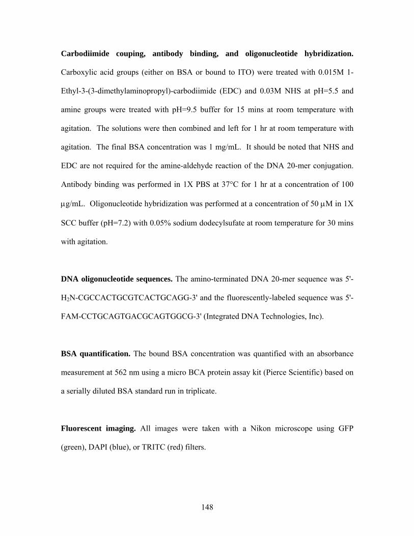
Carbodiimide couping, antibody binding, and oligonucleotide hybridization.
Carboxylic acid groups (either on BSA or bound to ITO) were treated with 0.015M 1-
Ethyl-3-(3-dimethylaminopropyl)-carbodiimide (EDC) and 0.03M NHS at pH=5.5 and
amine groups were treated with pH=9.5 buffer for 15 mins at room temperature with
agitation. The solutions were then combined and left for 1 hr at room temperature with
agitation. The final BSA concentration was 1 mg/mL. It should be noted that NHS and
EDC are not required for the amine-aldehyde reaction of the DNA 20-mer conjugation.
Antibody binding was performed in 1X PBS at 37°C for 1 hr at a concentration of 100
μg/mL. Oligonucleotide hybridization was performed at a concentration of 50 μM in 1X
SCC buffer (pH=7.2) with 0.05% sodium dodecylsufate at room temperature for 30 mins
with agitation.
DNA oligonucleotide sequences. The amino-terminated DNA 20-mer sequence was 5'-
H2N-CGCCACTGCGTCACTGCAGG-3' and the fluorescently-labeled sequence was 5'-
FAM-CCTGCAGTGACGCAGTGGCG-3' (Integrated DNA Technologies, Inc).
BSA quantification. The bound BSA concentration was quantified with an absorbance
measurement at 562 nm using a micro BCA protein assay kit (Pierce Scientific) based on
a serially diluted BSA standard run in triplicate.
Fluorescent imaging. All images were taken with a Nikon microscope using GFP
(green), DAPI (blue), or TRITC (red) filters.
148
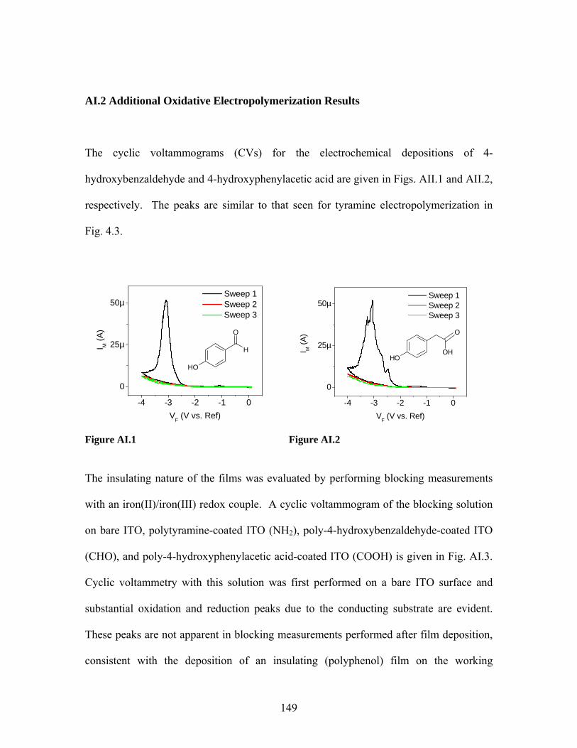
AI.2 Additional Oxidative Electropolymerization Results
The cyclic voltammograms (CVs) for the electrochemical depositions of 4-
hydroxybenzaldehyde and 4-hydroxyphenylacetic acid are given in Figs. AII.1 and AII.2,
respectively. The peaks are similar to that seen for tyramine electropolymerization in
Fig. 4.3.
-4 -3 -2 -1 0
0
25µ
50µ
OH
O
HI M (A
)
VF (V vs. Ref)
Sweep 1 Sweep 2 Sweep 3
-4 -3 -2 -1 0
0
25µ
50µ
OH
O
OHI M (A
)
VF (V vs. Ref)
Sweep 1 Sweep 2 Sweep 3
Figure AI.1 Figure AI.2
The insulating nature of the films was evaluated by performing blocking measurements
with an iron(II)/iron(III) redox couple. A cyclic voltammogram of the blocking solution
on bare ITO, polytyramine-coated ITO (NH2), poly-4-hydroxybenzaldehyde-coated ITO
(CHO), and poly-4-hydroxyphenylacetic acid-coated ITO (COOH) is given in Fig. AI.3.
Cyclic voltammetry with this solution was first performed on a bare ITO surface and
substantial oxidation and reduction peaks due to the conducting substrate are evident.
These peaks are not apparent in blocking measurements performed after film deposition,
consistent with the deposition of an insulating (polyphenol) film on the working
149
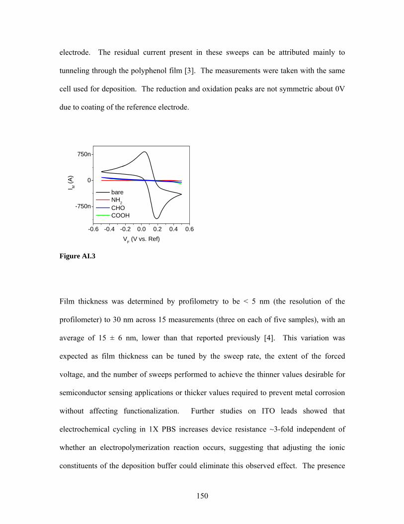
electrode. The residual current present in these sweeps can be attributed mainly to
tunneling through the polyphenol film [3]. The measurements were taken with the same
cell used for deposition. The reduction and oxidation peaks are not symmetric about 0V
due to coating of the reference electrode.
-0.6 -0.4 -0.2 0.0 0.2 0.4 0.6
-750n
0
750n
I M (A
)
VF (V vs. Ref)
bare NH2 CHO COOH
Figure AI.3
Film thickness was determined by profilometry to be < 5 nm (the resolution of the
profilometer) to 30 nm across 15 measurements (three on each of five samples), with an
average of 15 ± 6 nm, lower than that reported previously [4]. This variation was
expected as film thickness can be tuned by the sweep rate, the extent of the forced
voltage, and the number of sweeps performed to achieve the thinner values desirable for
semiconductor sensing applications or thicker values required to prevent metal corrosion
without affecting functionalization. Further studies on ITO leads showed that
electrochemical cycling in 1X PBS increases device resistance ~3-fold independent of
whether an electropolymerization reaction occurs, suggesting that adjusting the ionic
constituents of the deposition buffer could eliminate this observed effect. The presence
150
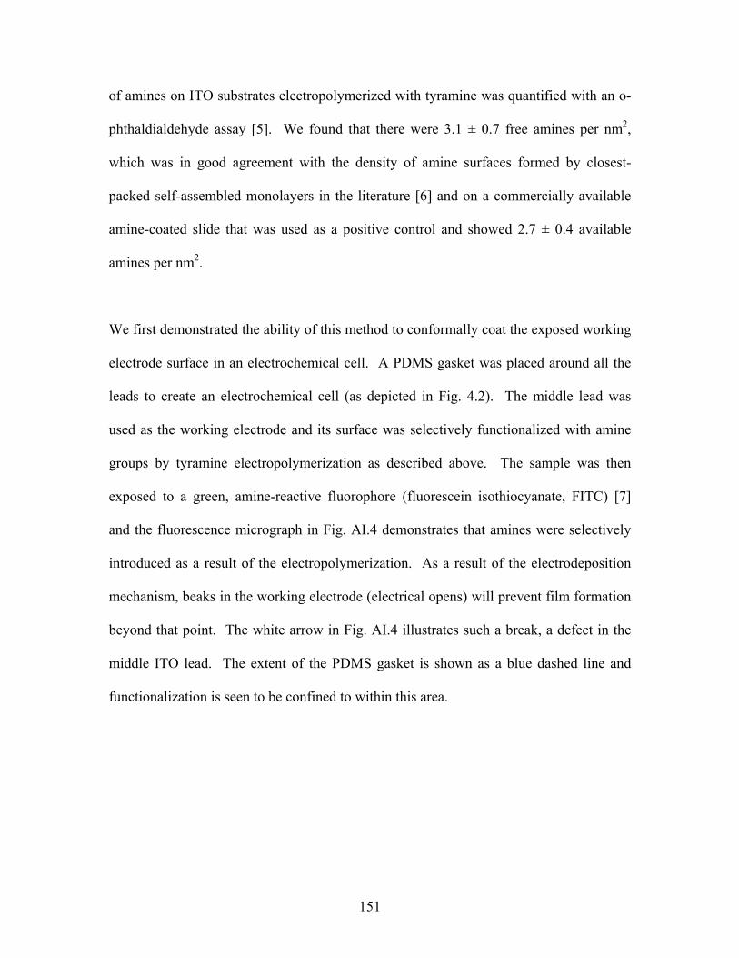
of amines on ITO substrates electropolymerized with tyramine was quantified with an o-
phthaldialdehyde assay [5]. We found that there were 3.1 ± 0.7 free amines per nm2,
which was in good agreement with the density of amine surfaces formed by closest-
packed self-assembled monolayers in the literature [6] and on a commercially available
amine-coated slide that was used as a positive control and showed 2.7 ± 0.4 available
amines per nm2.
We first demonstrated the ability of this method to conformally coat the exposed working
electrode surface in an electrochemical cell. A PDMS gasket was placed around all the
leads to create an electrochemical cell (as depicted in Fig. 4.2). The middle lead was
used as the working electrode and its surface was selectively functionalized with amine
groups by tyramine electropolymerization as described above. The sample was then
exposed to a green, amine-reactive fluorophore (fluorescein isothiocyanate, FITC) [7]
and the fluorescence micrograph in Fig. AI.4 demonstrates that amines were selectively
introduced as a result of the electropolymerization. As a result of the electrodeposition
mechanism, beaks in the working electrode (electrical opens) will prevent film formation
beyond that point. The white arrow in Fig. AI.4 illustrates such a break, a defect in the
middle ITO lead. The extent of the PDMS gasket is shown as a blue dashed line and
functionalization is seen to be confined to within this area.
151
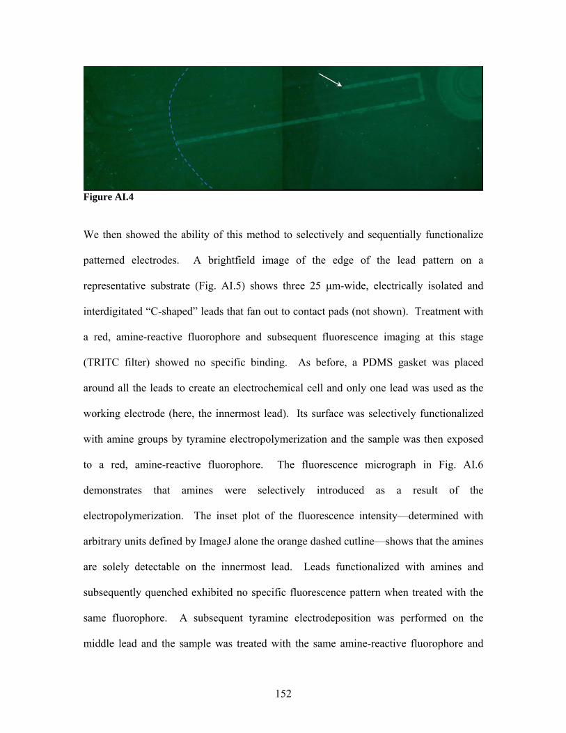
Figure AI.4
We then showed the ability of this method to selectively and sequentially functionalize
patterned electrodes. A brightfield image of the edge of the lead pattern on a
representative substrate (Fig. AI.5) shows three 25 μm-wide, electrically isolated and
interdigitated “C-shaped” leads that fan out to contact pads (not shown). Treatment with
a red, amine-reactive fluorophore and subsequent fluorescence imaging at this stage
(TRITC filter) showed no specific binding. As before, a PDMS gasket was placed
around all the leads to create an electrochemical cell and only one lead was used as the
working electrode (here, the innermost lead). Its surface was selectively functionalized
with amine groups by tyramine electropolymerization and the sample was then exposed
to a red, amine-reactive fluorophore. The fluorescence micrograph in Fig. AI.6
demonstrates that amines were selectively introduced as a result of the
electropolymerization. The inset plot of the fluorescence intensity—determined with
arbitrary units defined by ImageJ alone the orange dashed cutline—shows that the amines
are solely detectable on the innermost lead. Leads functionalized with amines and
subsequently quenched exhibited no specific fluorescence pattern when treated with the
same fluorophore. A subsequent tyramine electrodeposition was performed on the
middle lead and the sample was treated with the same amine-reactive fluorophore and
152
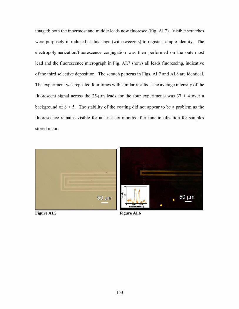
imaged; both the innermost and middle leads now fluoresce (Fig. AI.7). Visible scratches
were purposely introduced at this stage (with tweezers) to register sample identity. The
electropolymerization/fluorescence conjugation was then performed on the outermost
lead and the fluorescence micrograph in Fig. AI.7 shows all leads fluorescing, indicative
of the third selective deposition. The scratch patterns in Figs. AI.7 and AI.8 are identical.
The experiment was repeated four times with similar results. The average intensity of the
fluorescent signal across the 25-μm leads for the four experiments was 37 ± 4 over a
background of 8 ± 5. The stability of the coating did not appear to be a problem as the
fluorescence remains visible for at least six months after functionalization for samples
stored in air.
Figure AI.5 Figure AI.6
153
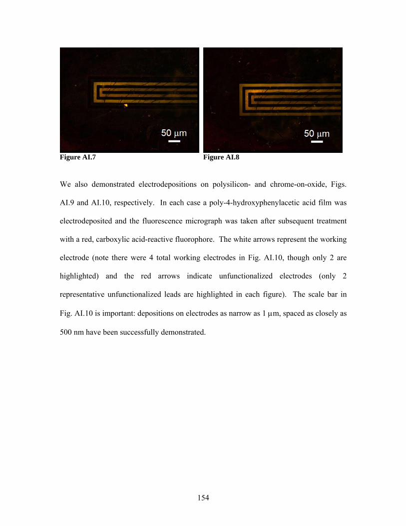
Figure AI.7 Figure AI.8
We also demonstrated electrodepositions on polysilicon- and chrome-on-oxide, Figs.
AI.9 and AI.10, respectively. In each case a poly-4-hydroxyphenylacetic acid film was
electrodeposited and the fluorescence micrograph was taken after subsequent treatment
with a red, carboxylic acid-reactive fluorophore. The white arrows represent the working
electrode (note there were 4 total working electrodes in Fig. AI.10, though only 2 are
highlighted) and the red arrows indicate unfunctionalized electrodes (only 2
representative unfunctionalized leads are highlighted in each figure). The scale bar in
Fig. AI.10 is important: depositions on electrodes as narrow as 1 μm, spaced as closely as
500 nm have been successfully demonstrated.
154
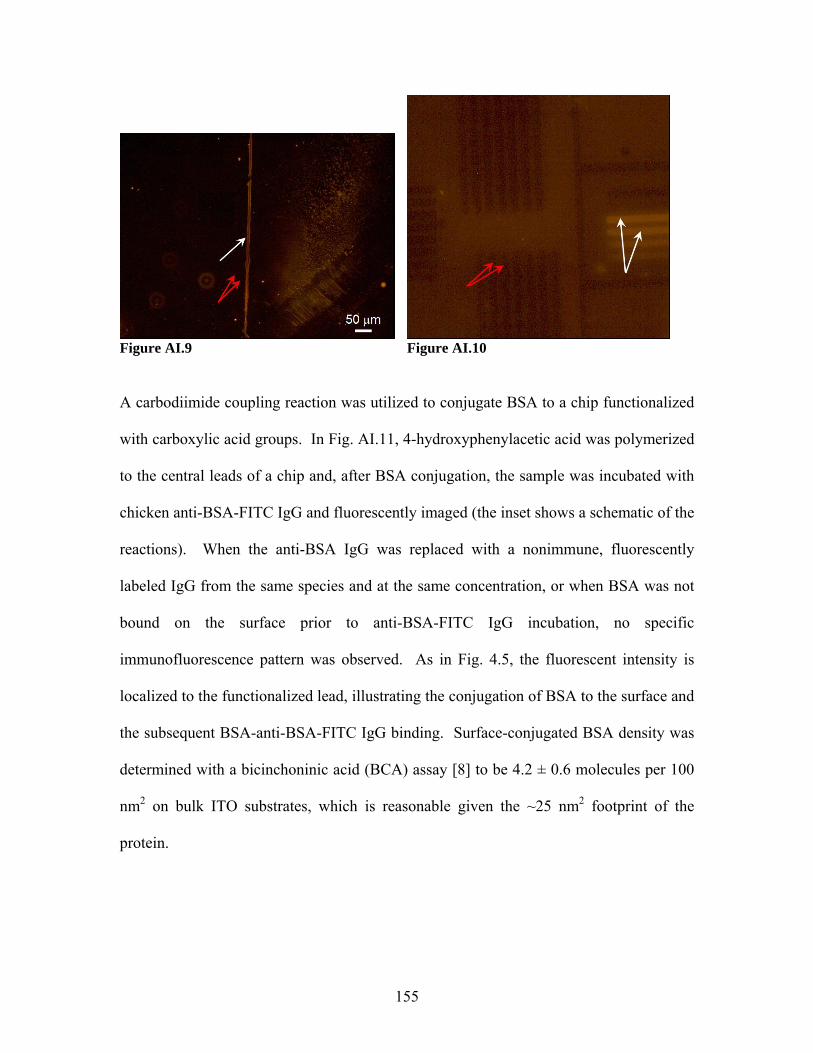
Figure AI.9 Figure AI.10
A carbodiimide coupling reaction was utilized to conjugate BSA to a chip functionalized
with carboxylic acid groups. In Fig. AI.11, 4-hydroxyphenylacetic acid was polymerized
to the central leads of a chip and, after BSA conjugation, the sample was incubated with
chicken anti-BSA-FITC IgG and fluorescently imaged (the inset shows a schematic of the
reactions). When the anti-BSA IgG was replaced with a nonimmune, fluorescently
labeled IgG from the same species and at the same concentration, or when BSA was not
bound on the surface prior to anti-BSA-FITC IgG incubation, no specific
immunofluorescence pattern was observed. As in Fig. 4.5, the fluorescent intensity is
localized to the functionalized lead, illustrating the conjugation of BSA to the surface and
the subsequent BSA-anti-BSA-FITC IgG binding. Surface-conjugated BSA density was
determined with a bicinchoninic acid (BCA) assay [8] to be 4.2 ± 0.6 molecules per 100
nm2 on bulk ITO substrates, which is reasonable given the ~25 nm2 footprint of the
protein.
155
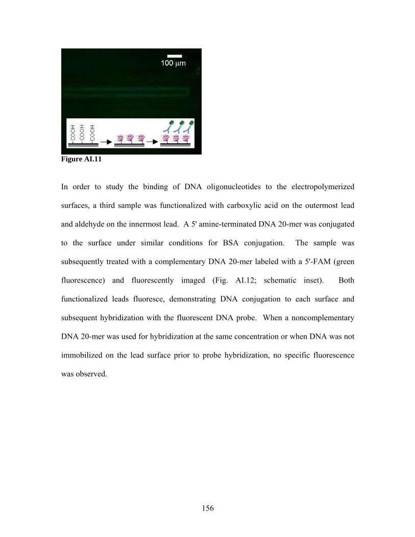
Figure AI.11
In order to study the binding of DNA oligonucleotides to the electropolymerized
surfaces, a third sample was functionalized with carboxylic acid on the outermost lead
and aldehyde on the innermost lead. A 5' amine-terminated DNA 20-mer was conjugated
to the surface under similar conditions for BSA conjugation. The sample was
subsequently treated with a complementary DNA 20-mer labeled with a 5'-FAM (green
fluorescence) and fluorescently imaged (Fig. AI.12; schematic inset). Both
functionalized leads fluoresce, demonstrating DNA conjugation to each surface and
subsequent hybridization with the fluorescent DNA probe. When a noncomplementary
DNA 20-mer was used for hybridization at the same concentration or when DNA was not
immobilized on the lead surface prior to probe hybridization, no specific fluorescence
was observed.
156
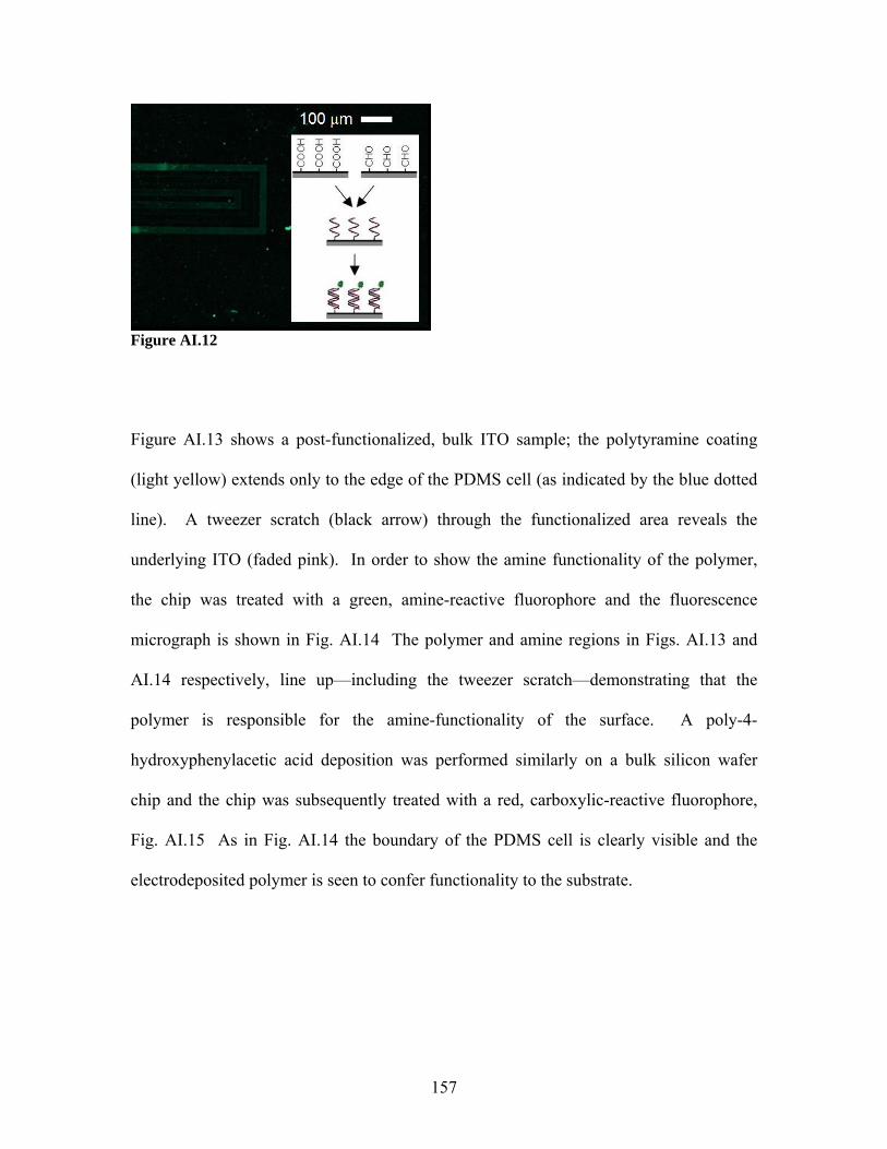
Figure AI.12
Figure AI.13 shows a post-functionalized, bulk ITO sample; the polytyramine coating
(light yellow) extends only to the edge of the PDMS cell (as indicated by the blue dotted
line). A tweezer scratch (black arrow) through the functionalized area reveals the
underlying ITO (faded pink). In order to show the amine functionality of the polymer,
the chip was treated with a green, amine-reactive fluorophore and the fluorescence
micrograph is shown in Fig. AI.14 The polymer and amine regions in Figs. AI.13 and
AI.14 respectively, line up—including the tweezer scratch—demonstrating that the
polymer is responsible for the amine-functionality of the surface. A poly-4-
hydroxyphenylacetic acid deposition was performed similarly on a bulk silicon wafer
chip and the chip was subsequently treated with a red, carboxylic-reactive fluorophore,
Fig. AI.15 As in Fig. AI.14 the boundary of the PDMS cell is clearly visible and the
electrodeposited polymer is seen to confer functionality to the substrate.
157
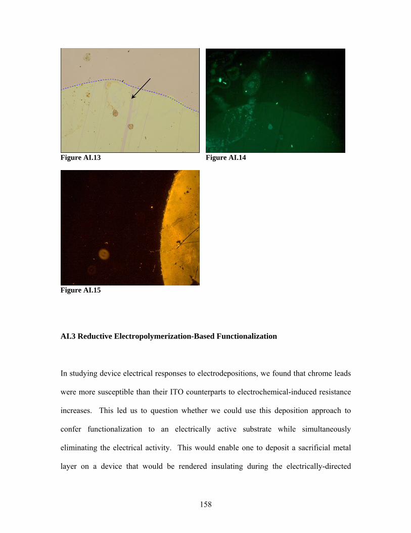
Figure AI.13 Figure AI.14
Figure AI.15
AI.3 Reductive Electropolymerization-Based Functionalization
In studying device electrical responses to electrodepositions, we found that chrome leads
were more susceptible than their ITO counterparts to electrochemical-induced resistance
increases. This led us to question whether we could use this deposition approach to
confer functionalization to an electrically active substrate while simultaneously
eliminating the electrical activity. This would enable one to deposit a sacrificial metal
layer on a device that would be rendered insulating during the electrically-directed
158
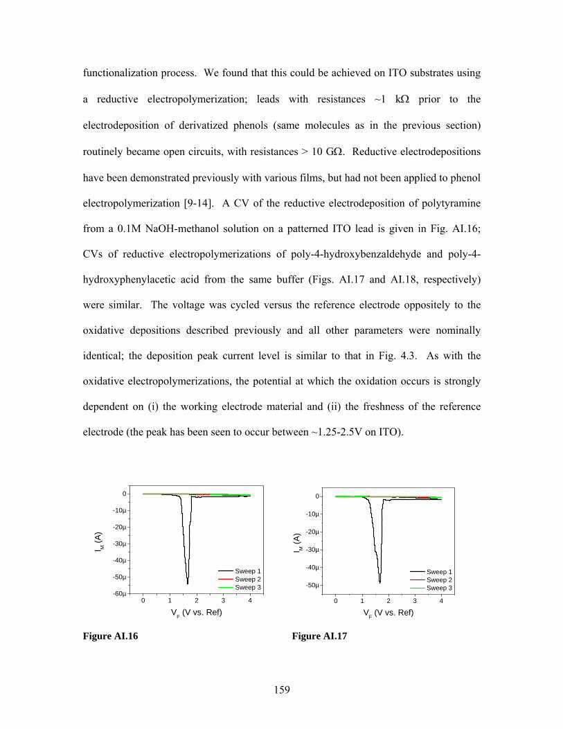
functionalization process. We found that this could be achieved on ITO substrates using
a reductive electropolymerization; leads with resistances ~1 kΩ prior to the
electrodeposition of derivatized phenols (same molecules as in the previous section)
routinely became open circuits, with resistances > 10 GΩ. Reductive electrodepositions
have been demonstrated previously with various films, but had not been applied to phenol
electropolymerization [9-14]. A CV of the reductive electrodeposition of polytyramine
from a 0.1M NaOH-methanol solution on a patterned ITO lead is given in Fig. AI.16;
CVs of reductive electropolymerizations of poly-4-hydroxybenzaldehyde and poly-4-
hydroxyphenylacetic acid from the same buffer (Figs. AI.17 and AI.18, respectively)
were similar. The voltage was cycled versus the reference electrode oppositely to the
oxidative depositions described previously and all other parameters were nominally
identical; the deposition peak current level is similar to that in Fig. 4.3. As with the
oxidative electropolymerizations, the potential at which the oxidation occurs is strongly
dependent on (i) the working electrode material and (ii) the freshness of the reference
electrode (the peak has been seen to occur between ~1.25-2.5V on ITO).
0 1 2 3 4-60µ
-50µ
-40µ
-30µ
-20µ
-10µ
0
I M (A
)
VF (V vs. Ref)
Sweep 1 Sweep 2 Sweep 3
0 1 2 3 4
-50µ
-40µ
-30µ
-20µ
-10µ
0
I M (A
)
VF (V vs. Ref)
Sweep 1 Sweep 2 Sweep 3
Figure AI.16 Figure AI.17
159
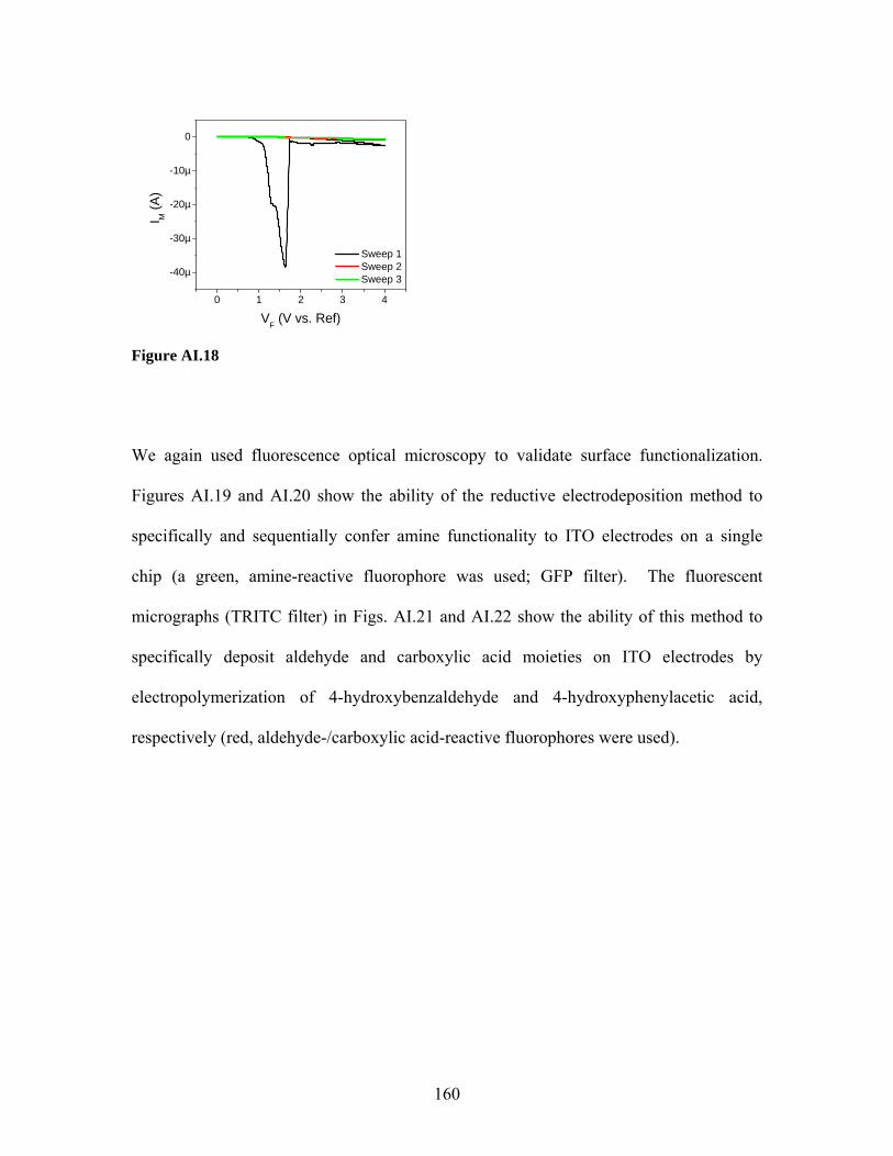
0 1 2 3 4
-40µ
-30µ
-20µ
-10µ
0
I M (A
)
VF (V vs. Ref)
Sweep 1 Sweep 2 Sweep 3
Figure AI.18
We again used fluorescence optical microscopy to validate surface functionalization.
Figures AI.19 and AI.20 show the ability of the reductive electrodeposition method to
specifically and sequentially confer amine functionality to ITO electrodes on a single
chip (a green, amine-reactive fluorophore was used; GFP filter). The fluorescent
micrographs (TRITC filter) in Figs. AI.21 and AI.22 show the ability of this method to
specifically deposit aldehyde and carboxylic acid moieties on ITO electrodes by
electropolymerization of 4-hydroxybenzaldehyde and 4-hydroxyphenylacetic acid,
respectively (red, aldehyde-/carboxylic acid-reactive fluorophores were used).
160
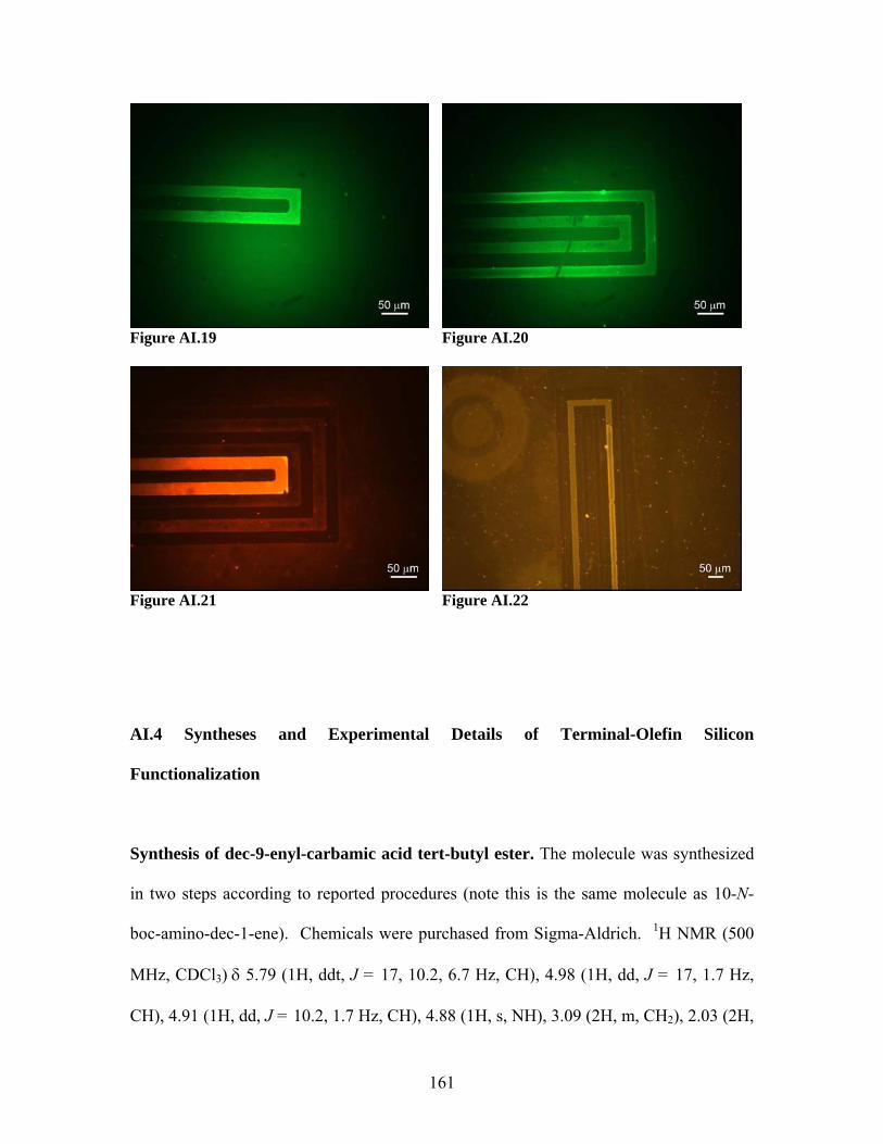
Figure AI.19 Figure AI.20
Figure AI.21 Figure AI.22
AI.4 Syntheses and Experimental Details of Terminal-Olefin Silicon
Functionalization
Synthesis of dec-9-enyl-carbamic acid tert-butyl ester. The molecule was synthesized
in two steps according to reported procedures (note this is the same molecule as 10-N-
boc-amino-dec-1-ene). Chemicals were purchased from Sigma-Aldrich. 1H NMR (500
MHz, CDCl3) δ 5.79 (1H, ddt, J = 17, 10.2, 6.7 Hz, CH), 4.98 (1H, dd, J = 17, 1.7 Hz,
CH), 4.91 (1H, dd, J = 10.2, 1.7 Hz, CH), 4.88 (1H, s, NH), 3.09 (2H, m, CH ), 2.03 (2H, 2
161
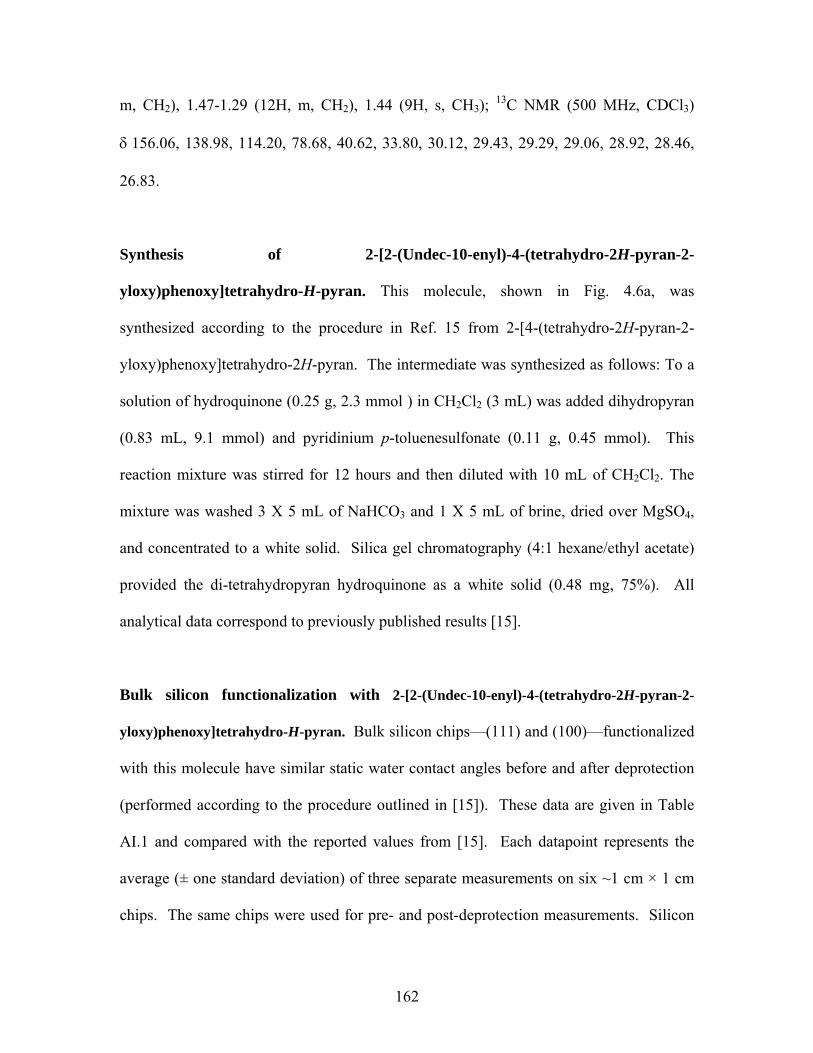
13m, CH ), 1.47-1.29 (12H, m, CH ), 1.44 (9H, s, CH ); C NMR (500 MHz, CDCl2 2 3 3)
δ 156.06, 138.98, 114.20, 78.68, 40.62, 33.80, 30.12, 29.43, 29.29, 29.06, 28.92, 28.46,
26.83.
Synthesis of 2-[2-(Undec-10-enyl)-4-(tetrahydro-2H-pyran-2-
yloxy)phenoxy]tetrahydro-H-pyran. This molecule, shown in Fig. 4.6a, was
synthesized according to the procedure in Ref. 15 from 2-[4-(tetrahydro-2H-pyran-2-
yloxy)phenoxy]tetrahydro-2H-pyran. The intermediate was synthesized as follows: To a
solution of hydroquinone (0.25 g, 2.3 mmol ) in CH Cl2 2 (3 mL) was added dihydropyran
(0.83 mL, 9.1 mmol) and pyridinium p-toluenesulfonate (0.11 g, 0.45 mmol). This
reaction mixture was stirred for 12 hours and then diluted with 10 mL of CH Cl2 2. The
mixture was washed 3 X 5 mL of NaHCO and 1 X 5 mL of brine, dried over MgSO3 4,
and concentrated to a white solid. Silica gel chromatography (4:1 hexane/ethyl acetate)
provided the di-tetrahydropyran hydroquinone as a white solid (0.48 mg, 75%). All
analytical data correspond to previously published results [15].
Bulk silicon functionalization with 2-[2-(Undec-10-enyl)-4-(tetrahydro-2H-pyran-2-
yloxy)phenoxy]tetrahydro-H-pyran. Bulk silicon chips—(111) and (100)—functionalized
with this molecule have similar static water contact angles before and after deprotection
(performed according to the procedure outlined in [15]). These data are given in Table
AI.1 and compared with the reported values from [15]. Each datapoint represents the
average (± one standard deviation) of three separate measurements on six ~1 cm × 1 cm
chips. The same chips were used for pre- and post-deprotection measurements. Silicon
162
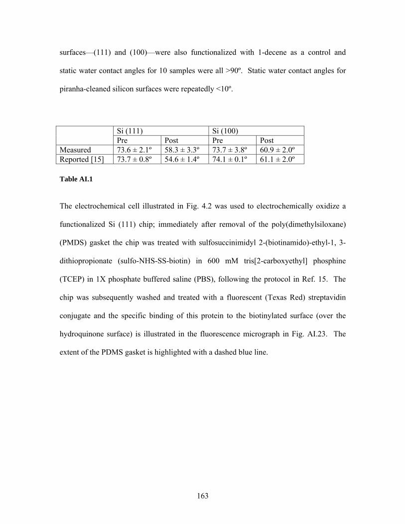
surfaces—(111) and (100)—were also functionalized with 1-decene as a control and
static water contact angles for 10 samples were all >90º. Static water contact angles for
piranha-cleaned silicon surfaces were repeatedly <10º.
Si (111) Si (100) Pre Post Pre Post
Measured 73.6 ± 2.1º 58.3 ± 3.3º 73.7 ± 3.8º 60.9 ± 2.0º
Table AI.1
The electrochemical cell illustrated in Fig. 4.2 was used to electrochemically oxidize a
functionalized Si (111) chip; immediately after removal of the poly(dimethylsiloxane)
(PMDS) gasket the chip was treated with sulfosuccinimidyl 2-(biotinamido)-ethyl-1, 3-
dithiopropionate (sulfo-NHS-SS-biotin) in 600 mM tris[2-carboxyethyl] phosphine
(TCEP) in 1X phosphate buffered saline (PBS), following the protocol in Ref. 15. The
chip was subsequently washed and treated with a fluorescent (Texas Red) streptavidin
conjugate and the specific binding of this protein to the biotinylated surface (over the
hydroquinone surface) is illustrated in the fluorescence micrograph in Fig. AI.23. The
extent of the PDMS gasket is highlighted with a dashed blue line.
Reported [15] 73.7 ± 0.8º 54.6 ± 1.4º 74.1 ± 0.1º 61.1 ± 2.0º
163
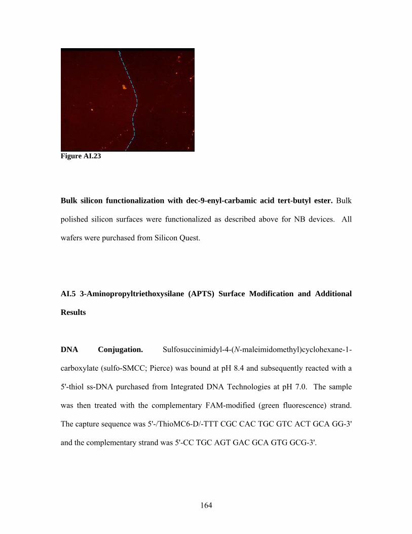
Figure AI.23
Bulk silicon functionalization with dec-9-enyl-carbamic acid tert-butyl ester. Bulk
polished silicon surfaces were functionalized as described above for NB devices. All
wafers were purchased from Silicon Quest.
AI.5 3-Aminopropyltriethoxysilane (APTS) Surface Modification and Additional
Results
DNA Conjugation. Sulfosuccinimidyl-4-(N-maleimidomethyl)cyclohexane-1-
carboxylate (sulfo-SMCC; Pierce) was bound at pH 8.4 and subsequently reacted with a
5'-thiol ss-DNA purchased from Integrated DNA Technologies at pH 7.0. The sample
was then treated with the complementary FAM-modified (green fluorescence) strand.
The capture sequence was 5'-/ThioMC6-D/-TTT CGC CAC TGC GTC ACT GCA GG-3'
and the complementary strand was 5'-CC TGC AGT GAC GCA GTG GCG-3'.
164
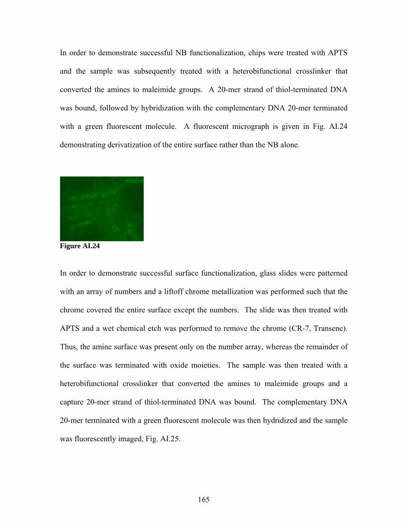
In order to demonstrate successful NB functionalization, chips were treated with APTS
and the sample was subsequently treated with a heterobifunctional crosslinker that
converted the amines to maleimide groups. A 20-mer strand of thiol-terminated DNA
was bound, followed by hybridization with the complementary DNA 20-mer terminated
with a green fluorescent molecule. A fluorescent micrograph is given in Fig. AI.24
demonstrating derivatization of the entire surface rather than the NB alone.
Figure AI.24
In order to demonstrate successful surface functionalization, glass slides were patterned
with an array of numbers and a liftoff chrome metallization was performed such that the
chrome covered the entire surface except the numbers. The slide was then treated with
APTS and a wet chemical etch was performed to remove the chrome (CR-7, Transene).
Thus, the amine surface was present only on the number array, whereas the remainder of
the surface was terminated with oxide moieties. The sample was then treated with a
heterobifunctional crosslinker that converted the amines to maleimide groups and a
capture 20-mer strand of thiol-terminated DNA was bound. The complementary DNA
20-mer terminated with a green fluorescent molecule was then hydridized and the sample
was fluorescently imaged, Fig. AI.25.
165

Figure AI.25
166
References
1. Guenbour, A., Kacemi, A., & Benbachir, A. Corrosion protection of copper by
polyaminophenol films. Prog. Org. Coat. 39, 151-155 (2000).
2. Pham, M. C., DuBois, J.-E., Lacaze, P.-C. Obtaining thin films of “reactive
polymers” on metal surfaces by electrochemical polymerization part II. Alcohol
substituted polyphenylene oxide films. J. Electroanal. Chem. 99, 331-340 (1979).
3. Gao, Z. & Siow, K. S. Ultramicroelectrode ensembles based on self-assembled
polymericmonolayers on gold electrodes. Electrochim. Acta 42, 315-321 (1997).
4. Dubois, J.-E., Lacaze, P.-C. & Pham, M. C. Obtaining thin films of “reactive
polymers” on metal surfaces by electrochemical polymerization part III. Amino-
substituted polyphenylene oxide films. Application to preparation of ferrocene
electroactive films. J. Electroanal. Chem. 117, 233-241 (1981).
5. Buck, R. H. & Krummen, K. High-performance liquid chromatographic
determination of enantiomeric amino acids and amino alcohols after
derivatization with o-phthaldialdehyde and various chiral mercaptans: application
to peptide hydrolysates. J. Chromatogr. 387, 255-265 (1987).
6. Lateef, S. S. et al. Three-dimensional chemical structures by protein
functionalized micron-sized beads bound to polylysine coated silicone surfaces. J.
Biomed. Mat. Res. A 72A, 373-380 (2005).
7. Hermanson, G. T. Bioconjugate Techniques. (Academic Press, New York, 1996).
8. Smith, P. K. et al. Measurement of protein using bicinchoninic acid. Anal.
Biochem. 150, 76-85 (1985).
167
9. Park, S. et al. Assignments of cyclic voltammetric peaks during electrochemical
polymerization of pyrrole with viologen pendant. Syn. Metals 139, 439-443
(2003).
10. Cosnier, S. et al. A poly(pyrrole-cobalt(II)deuteroporphyrin) electrode for the
potentiometric determination of nitrite. Sensors 3, 213-222 (2003).
11. Damlin, P. et al. In situ spectroelectrochemical and rotating-disk electrode studies
on the initial states in the reuctive electropolymerization of poly(p-phenylene
vinylene). Macromolecules 35, 5789-1795 (2002).
12. Ontko, A. C., Armistead, P. M., Kircus, S. R. & Thorp, H. H. Electrochemical
detection of single-stranded DNA using polymer-modified electrodes. Inorg.
Chem. 38, 1842-1846 (1999).
13. Tanaka, S. & Iso, T. Reductive electropolymerization of 2,5-dichlorobenzonitrile.
J. Chem. Soc.-Chem. Comm. 9, 1071-1072 (1994).
14. Gould, S. et al. Reductive electropolymerization of complexes containing an
aldehyde-substituted derivative of 2,2’-bipyridine. J. Electroanal. Chem. 350,
143-159 (1993).
15. Bunimovich, Y.L. et al. Electrochemically programmed, spatially selective
biofunctionalization of silicon wires. Langmuir 20, 10630-10638 (2004).
168
Appendix II: Sensing Methods
AII.1 Unfunctionalized Nanobar Sensing Methods
General sensing considerations. The initial sensor equilibration time is not shown. For
all measurements ISD was measured at 0.25 sec intervals while VSD and VGD were held
constant; V was set to -5V and VSD GD to -33V. The active region of all devices used for
sensing experiments was 10 μm in length. The solutions were titrated from 1X PBS
(phosphate buffered saline), pH 7.4, and were correct to ±0.02. Mixing was continued
after injection of the solution of interest.
Mice. All animals were routinely used at 6-8 weeks of age and were maintained under
specific pathogen free conditions and routinely checked by the Yale University Animal
Resource Center. OT-1 transgenic breeder mice were a gift from (Ruslan Medzhitov,
Yale) and 2C TCR animals were gift from (Herman Eisen, MIT). C57/BL6 (B6) mice
were obtained from Jackson Laboratories (Bar Harbor, ME). All transgenic mice were
maintained as heterozygous by breading on a B6 background in our animal facility.
Phenotypes were tested with the clonotypic 1B2 antibody (for 2C mice) and Valpha and
CD8 for OT-1.
Cells. All cells used were obtained from homogenized naive mouse spleens after
depletion of RBC by hypotonic lysis (Acros organics). Splenocytes were used without
169
further purification. For experiments involving inhibition of cellular signaling, 1 mL of 1
mg/mL genistein (Quality Biological) was added to splenocytes at 1 × 10⁷ cells/mL
followed by incubation for 1 hr at 4°C. Cell viability was assessed with trypan blue
before and after genistein treatment.
Sensing measurements. The low-buffered solution was created by diluting 1X PBS
tenfold and adding sodium chloride to a final concentration of 150 mM. Cells were
resuspended in this solution immediately prior to sensing measurements at a
concentration of 1 × 10⁷ cells/mL. 7 μL of this solution was initially present in the sensor
reservoir for all cellular measurements, thus ~7 × 10⁴ total cells were present. 2 μL of
stimulant (anti-CD3 or peptide/MHC dimmer, a gift from Jonathan Schneck-Johns
Hopkins School of Medicine) was added at a concentration of 0.5 mg/mL for all cellular
measurements. Mixing was induced throughout the measurement.
AII.2 Functionalized Nanobar Sensing Methods
Functionalized Sensing. For functionalized-sensor measurements VSD was set to -2V and
V to -20V because experiments showed that VGD GD = -20V was the optimal gate voltage.
For studies involving macromolecule addition, time = 0 is defined as the onset of
protein/DNA addition. In all plots the initial sensor equilibration time is not shown.
Experiments were run for ~100 sec and mixing was continued after injection of the
solution of interest.
170
Macromolecule Sensing. All devices used for functionalized-sensing experiments were
nominally similar, with t = 40 nm and w within 50-150 nm. Each measurement was
produced by a single device; the device-to-device variation in sensor response is within
20%. For all sensing experiments, the volume of liquid in the solution chamber was ~10
μL, starting with 10 μL of buffer and displacing this with 100 μL of protein/DNA
solution, of which 10 μL remained.
Biotin-Streptavidin/Avidin Sensing. We used 0.1X PBS, pH 7.4, for all biotin sensing
experiments (unless otherwise noted); for 0.1X PBS, λD ~ 2.3 nm [1,2]. The pH 9.0 and
pH 10.5 solutions were mixed with similar salt concentrations, thus both have λD ~ 2.3
nm [1,2]. Biotinylation was performed with N-hydroxysulfosuccinimide (sulfo-NHS)-
biotin, sulfo-NHS-SS-biotin, or sulfo-NHS-LC-biotin (Pierce Chemical) at pH 10.5 (see
Appendix I). For Figs. 5.14 and 5.15, currents were normalized by dividing the measured
ISD by the pre-addition average current.
Antibody-Antigen Sensing. The capture antibodies were bound using NHS/ethylene
dicarbodiimide coupling (see Appendix I). The sensing was performed in a 1mM sodium
bicarbonate buffer, pH 8.4 (λD ~ 6.8 nm) [1,2].
DNA Sensing. Sulfosuccinimidyl-4-(N-maleimidomethyl)cyclohexane-1-carboxylate
(sulfo-SMCC; Pierce) was bound to two functionalized devices at pH 7.5 and
subsequently reacted with the 5'-thiol ss-DNA at pH 7.0 (see Appendix I). For sensing,
171
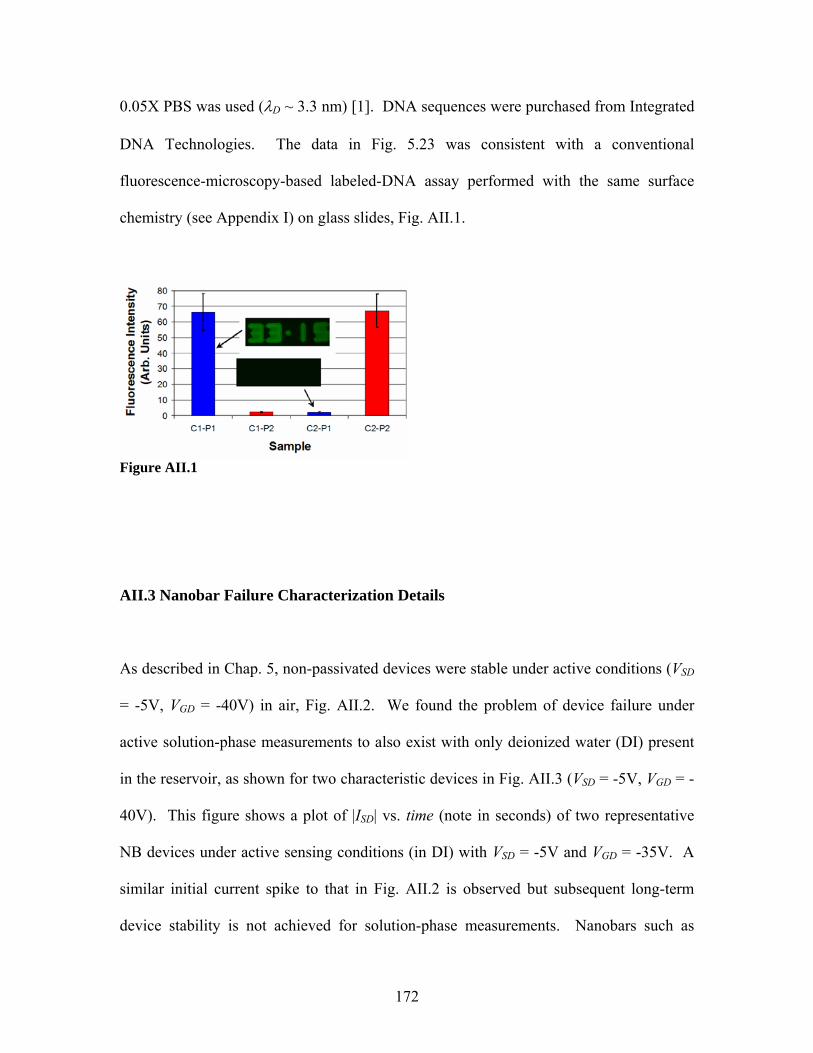
0.05X PBS was used (λD ~ 3.3 nm) [1]. DNA sequences were purchased from Integrated
DNA Technologies. The data in Fig. 5.23 was consistent with a conventional
fluorescence-microscopy-based labeled-DNA assay performed with the same surface
chemistry (see Appendix I) on glass slides, Fig. AII.1.
Figure AII.1
AII.3 Nanobar Failure Characterization Details
As described in Chap. 5, non-passivated devices were stable under active conditions (VSD
= -5V, VGD = -40V) in air, Fig. AII.2. We found the problem of device failure under
active solution-phase measurements to also exist with only deionized water (DI) present
in the reservoir, as shown for two characteristic devices in Fig. AII.3 (V = -5V, VSD GD = -
40V). This figure shows a plot of |ISD| vs. time (note in seconds) of two representative
NB devices under active sensing conditions (in DI) with VSD = -5V and VGD = -35V. A
similar initial current spike to that in Fig. AII.2 is observed but subsequent long-term
device stability is not achieved for solution-phase measurements. Nanobars such as
172
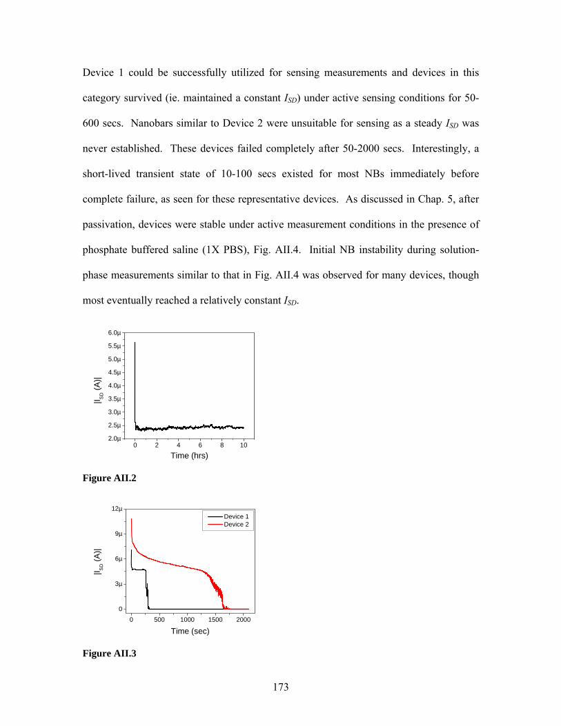
Device 1 could be successfully utilized for sensing measurements and devices in this
category survived (ie. maintained a constant ISD) under active sensing conditions for 50-
600 secs. Nanobars similar to Device 2 were unsuitable for sensing as a steady ISD was
never established. These devices failed completely after 50-2000 secs. Interestingly, a
short-lived transient state of 10-100 secs existed for most NBs immediately before
complete failure, as seen for these representative devices. As discussed in Chap. 5, after
passivation, devices were stable under active measurement conditions in the presence of
phosphate buffered saline (1X PBS), Fig. AII.4. Initial NB instability during solution-
phase measurements similar to that in Fig. AII.4 was observed for many devices, though
most eventually reached a relatively constant ISD.
0 2 4 6 8 102.0µ
2.5µ
3.0µ
3.5µ
4.0µ
4.5µ
5.0µ
5.5µ
6.0µ
|I SD (A
)|
Time (hrs)
Figure AII.2
0 500 1000 1500 2000
0
3µ
6µ
9µ
12µ
|I SD (A
)|
Time (sec)
Device 1 Device 2
Figure AII.3
173
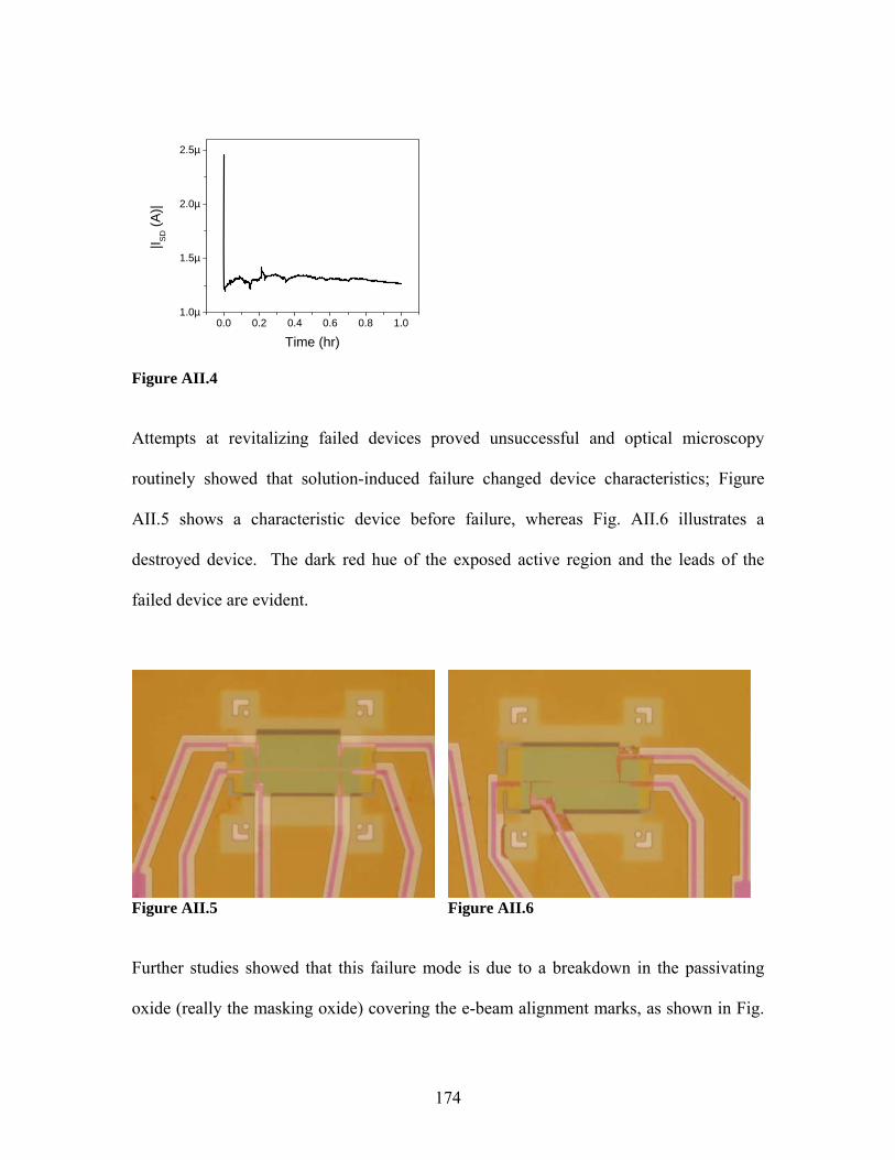
0.0 0.2 0.4 0.6 0.8 1.01.0µ
1.5µ
2.0µ
2.5µ|I S
D (A
)|
Time (hr)
Figure AII.4
Attempts at revitalizing failed devices proved unsuccessful and optical microscopy
routinely showed that solution-induced failure changed device characteristics; Figure
AII.5 shows a characteristic device before failure, whereas Fig. AII.6 illustrates a
destroyed device. The dark red hue of the exposed active region and the leads of the
failed device are evident.
Figure AII.5 Figure AII.6
Further studies showed that this failure mode is due to a breakdown in the passivating
oxide (really the masking oxide) covering the e-beam alignment marks, as shown in Fig.
174
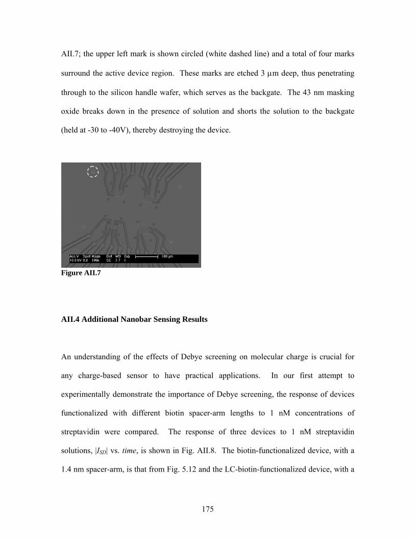
AII.7; the upper left mark is shown circled (white dashed line) and a total of four marks
surround the active device region. These marks are etched 3 μm deep, thus penetrating
through to the silicon handle wafer, which serves as the backgate. The 43 nm masking
oxide breaks down in the presence of solution and shorts the solution to the backgate
(held at -30 to -40V), thereby destroying the device.
Figure AII.7
AII.4 Additional Nanobar Sensing Results
An understanding of the effects of Debye screening on molecular charge is crucial for
any charge-based sensor to have practical applications. In our first attempt to
experimentally demonstrate the importance of Debye screening, the response of devices
functionalized with different biotin spacer-arm lengths to 1 nM concentrations of
streptavidin were compared. The response of three devices to 1 nM streptavidin
solutions, |ISD| vs. time, is shown in Fig. AII.8. The biotin-functionalized device, with a
1.4 nm spacer-arm, is that from Fig. 5.12 and the LC-biotin-functionalized device, with a
175
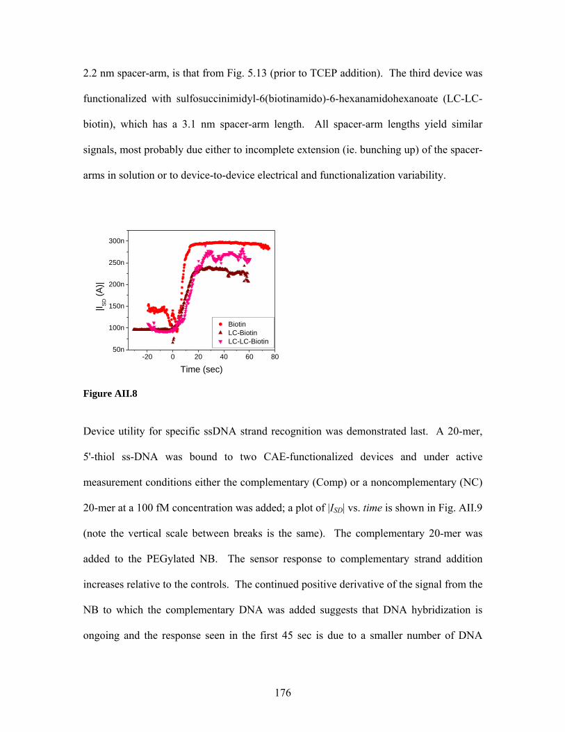
2.2 nm spacer-arm, is that from Fig. 5.13 (prior to TCEP addition). The third device was
functionalized with sulfosuccinimidyl-6(biotinamido)-6-hexanamidohexanoate (LC-LC-
biotin), which has a 3.1 nm spacer-arm length. All spacer-arm lengths yield similar
signals, most probably due either to incomplete extension (ie. bunching up) of the spacer-
arms in solution or to device-to-device electrical and functionalization variability.
-20 0 20 40 60 8050n
100n
150n
200n
250n
300n
|I SD (A
)|
Time (sec)
BiotinLC-BiotinLC-LC-Biotin
Figure AII.8
Device utility for specific ssDNA strand recognition was demonstrated last. A 20-mer,
5'-thiol ss-DNA was bound to two CAE-functionalized devices and under active
measurement conditions either the complementary (Comp) or a noncomplementary (NC)
20-mer at a 100 fM concentration was added; a plot of |ISD| vs. time is shown in Fig. AII.9
(note the vertical scale between breaks is the same). The complementary 20-mer was
added to the PEGylated NB. The sensor response to complementary strand addition
increases relative to the controls. The continued positive derivative of the signal from the
NB to which the complementary DNA was added suggests that DNA hybridization is
ongoing and the response seen in the first 45 sec is due to a smaller number of DNA
176
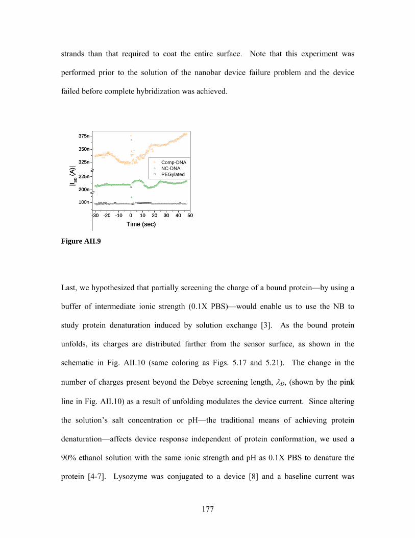
strands than that required to coat the entire surface. Note that this experiment was
performed prior to the solution of the nanobar device failure problem and the device
failed before complete hybridization was achieved.
-30 -20 -10 0 10 20 30 40 50
175n
200n
225n
325n
350n
375n
|I SD (A
)|
Time (sec)
Comp-DNA NC-DNA PEGylated
100n
-30 -20 -10 0 10 20 30 40 50
175n
200n
225n
325n
350n
375n
|I SD (A
)|
Time (sec)
Comp-DNA NC-DNA PEGylated
100n
Figure AII.9
Last, we hypothesized that partially screening the charge of a bound protein—by using a
buffer of intermediate ionic strength (0.1X PBS)—would enable us to use the NB to
study protein denaturation induced by solution exchange [3]. As the bound protein
unfolds, its charges are distributed farther from the sensor surface, as shown in the
schematic in Fig. AII.10 (same coloring as Figs. 5.17 and 5.21). The change in the
number of charges present beyond the Debye screening length, λD, (shown by the pink
line in Fig. AII.10) as a result of unfolding modulates the device current. Since altering
the solution’s salt concentration or pH—the traditional means of achieving protein
denaturation—affects device response independent of protein conformation, we used a
90% ethanol solution with the same ionic strength and pH as 0.1X PBS to denature the
protein [4-7]. Lysozyme was conjugated to a device [8] and a baseline current was
177
established in 0.1X PBS. After complete solution exchange with the ethanol denaturant
(beginning at time = 0), which required ~0.5 sec, the device current decreased to a stable
level in 3-4 steps, Fig. AII.11. The 90% ethanol solution contained 1% 1X PBS, thus λD
remained unchanged throughout the experiment. This decrease in |ISD| is due to the flux
of negative charge away from the sensor surface and beyond λD, which is consistent with
the denaturation of lysozyme, a negative protein with pI ~ 4.3. A control study with no
lysozyme bound showed no significant change in signal after solution exchange,
indicating that the ethanol solution affected the lysozyme rather than the device. The
stepwise fashion in which the signal intensity decreased suggests the presence of transient
intermediate conformations existing between the native and fully denatured states,
consistent with previous reports [9-11]. Additionally, the variance in step duration
suggests different transition state stabilities, as seen previously with optical methods [9-
11]. Although future work is required to fully understand these data, Fig. AII.11 shows
that NB sensors can be used as solid-state tools for studying protein folding.
178
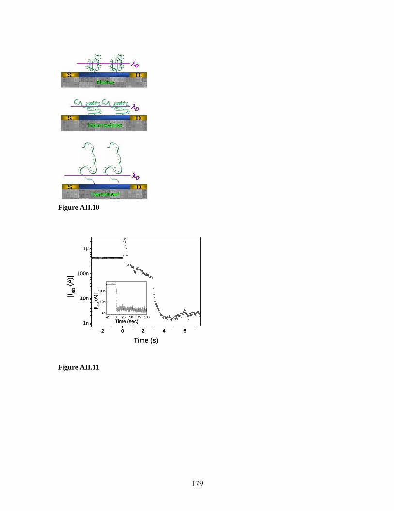
Figure AII.10
-2 0 2 4 61n
10n
100n
1µ
|I SD (A
)|
Time (s)
-25 0 25 50 75 1001n
10n
100n
|I SD (A
)|
Time (sec)
-2 0 2 4 61n
10n
100n
1µ
|I SD (A
)|
Time (s)
-25 0 25 50 75 1001n
10n
100n
|I SD (A
)|
Time (sec)
Figure AII.11
179
References
1. Stern, E. et al. Label-free immunodetection with nanowire CMOS-compatible
semiconducting nanowires. Nature 445, 519-522 (2007).
2. Israelachvili, J. N. Intermolecular and Surface Forces with Applications to
Colloidal and Biological Systems. (Academic Press, New York, 1985).
3. Voet, D. & Voet, J. G. Biochemistry. 2nd Edn. (John Wiley & Sons, New York,
1995).
4. Sasahara, K. & Katsutoshi, N. Effect of ethanol on folding of hen egg-white
lysozyme under acidic condition. Proteins: Struct. Funct. Bioinform. 63, 127-135
(2006).
5. Thomas, P. D. & Dill, D. A. Local and nonlocal interactions in global proteins
and mechanism of alcohol denaturation. Protein Sci. 2, 2050-2065 (1993).
6. Hirota, N., Mizuno, K. & Goto, Y. Group additive contributions to the alcohol-
induced α-helix formation of melittin: implication for the mechanism of the
alcohol effects on proteins. J. Mol. Biol. 275, 365-378 (1998).
7. Kamatari, Y. O., Konno, T., Kataoka, M. & Akasaka, K. The methanol-induced
transition and the expanded helical conformation in hen lysozyme. Protein Sci. 7,
681-688 (1998).
8. Hermanson, G. T. Bioconjugate Techniques (Elsevier Science & Technology
Books, New York, 1996).
180
9. Mizuguchi, M., Arai, M., Ke, Y., Nitta, K. & Kuwajima, K. Equilibrium and
kinetics of the folding of equine lysozyme studied by circular dichroism
spectroscopy. J. Mol. Biol. 283, 265-277 (1998).
10. Zaidi, F. N., Nath, U. & Udgaonkar, J. B. Multiple intermediates and transition
states during protein unfolding. Nature Struct. Biol. 4, 1016-1024 (1007).
11. Laurents, D. V. & Baldwin, R. L. Characterization of the unfolding pathway of
hen egg white lysozyme. Biochem. 36, 1496-1504 (1997).
181
Appendix III: Nanowire-Field Effect Transistors
AIII.1 Nanowire-FET Fabrication Overview
Owing to the lack of successful schemes NW alignment on planar substrates [1-12],
electron beam (e-beam) lithography is typically the method of choice for NW-FET
fabrication because it allows a specific lead pattern to be written for each NW, assuring
the geometric definition of successful contacts [13-24]. The inability to achieve parallel
device fabrication with this method prevented us from performing statistical studies,
which are required to thoroughly characterize nanoscale materials [25], and led us to
develop an optical lithographic approach [25,26].
The NWs we used [25-29] were grown in-house by the vapor-liquid-solid (VLS)
mechanism [13,18,24,25,27,28] and were fabricated into the NW-FETs required for
sensing by transferring them from their growth substrate to an oxide-coated,
degenerately-doped silicon wafer and performing microlithographic fabrication to define
source and drain contacts to the NW. A liftoff metallization was used for contact
definition to prevent NW exposure to metal etchants. Topside backgate contacts to the
degenerate silicon wafer were also fabricated, allowing for high-throughput device
characterization in a configuration suitable for sensing [25-29].
182
The primary advantage of the e-beam contacting method is that the NW suspension can
be applied to the wafer multiple times until the NW density in the e-beam writing
window (checked with an optical or scanning electron microscope, SEM) is sufficient to
guarantee successful NW-FET fabrication. Thus, this dispersion method proved
relatively insensitive to growth yield (compared with the optical approach) because of the
potential deposition/screening iterations and because NWs lying in any orientation in the
e-beam window could be contacted. However, this method is labor intense, thereby
limiting the number of devices that can be fabricated, and pre-selection of NWs, whereby
the best NWs are fabricated into devices, is extremely difficult to avoid. A representative
4-point e-beam-defined NW-FET is shown in Fig. AIII.1 [26,29].
In contrast, the optical processing method enables parallel NW-FET fabrication across an
entire wafer and, in turn, eliminates the pre-selection inherent in the e-beam fabrication
process. However, there are two key limitations to this high-throughput method: the
NWs must be at least ~3 μm long (ideally > 5 μm) to span the leads, which are spaced 2-
3 μm due to contact lithography limitations, and the NW density must be high in order to
obtain devices since the leads cover 1.6% or 2.4% of the chip’s area for the 2 and 3 μm
patterns, respectively [25-29]. Samples with low NW yields were sometimes
successfully fabricated by applying multiple drops of the NW suspension to the wafer but
a certain density threshold was required in order to obtain devices. The NW density must
also be sufficiently low such that the majority of devices were due to an individual NW,
thus the density must be carefully chosen to lie within these boundaries. A 7-point
optically-defined NW-FET is shown in Fig. AIII.2 [25-29]. Figure AIII.2 gives a
183
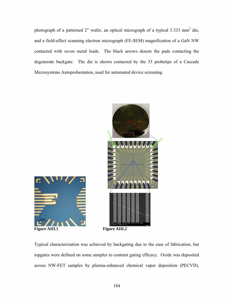
photograph of a patterned 2” wafer, an optical micrograph of a typical 3.333 mm2 die,
and a field-effect scanning electron micrograph (FE-SEM) magnification of a GaN NW
contacted with seven metal leads. The black arrows denote the pads contacting the
degenerate backgate. The die is shown contacted by the 33 probetips of a Cascade
Microsystems Autoprobestation, used for automated device screening.
Figure AIII.1 Figure AIII.2
Typical characterization was achieved by backgating due to the ease of fabrication, but
topgates were defined on some samples to contrast gating efficacy. Oxide was deposited
across NW-FET samples by plasma-enhanced chemical vapor deposition (PECVD),
184
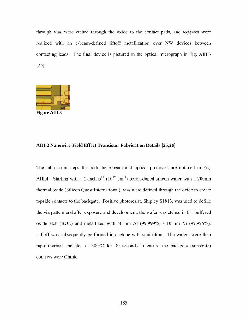
through vias were etched through the oxide to the contact pads, and topgates were
realized with an e-beam-defined liftoff metallization over NW devices between
contacting leads. The final device is pictured in the optical micrograph in Fig. AIII.3
[25].
Figure AIII.3
AIII.2 Nanowire-Field Effect Transistor Fabrication Details [25,26]
The fabrication steps for both the e-beam and optical processes are outlined in Fig.
AIII.4. Starting with a 2-inch p++ (1019 cm-3) boron-doped silicon wafer with a 200nm
thermal oxide (Silicon Quest International), vias were defined through the oxide to create
topside contacts to the backgate. Positive photoresist, Shipley S1813, was used to define
the via pattern and after exposure and development, the wafer was etched in 6:1 buffered
oxide etch (BOE) and metallized with 50 nm Al (99.999%) / 10 nm Ni (99.995%).
Liftoff was subsequently performed in acetone with sonication. The wafers were then
rapid-thermal annealed at 300°C for 30 seconds to ensure the backgate (substrate)
contacts were Ohmic.
185
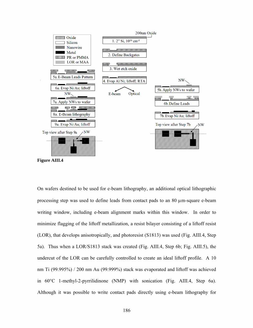
Figure AIII.4
On wafers destined to be used for e-beam lithography, an additional optical lithographic
processing step was used to define leads from contact pads to an 80 μm-square e-beam
writing window, including e-beam alignment marks within this window. In order to
minimize flagging of the liftoff metallization, a resist bilayer consisting of a liftoff resist
(LOR), that develops anisotropically, and photoresist (S1813) was used (Fig. AIII.4, Step
5a). Thus when a LOR/S1813 stack was created (Fig. AIII.4, Step 6b; Fig. AIII.5), the
undercut of the LOR can be carefully controlled to create an ideal liftoff profile. A 10
nm Ti (99.995%) / 200 nm Au (99.999%) stack was evaporated and liftoff was achieved
in 60°C 1-methyl-2-pyrrilidinone (NMP) with sonication (Fig. AIII.4, Step 6a).
Although it was possible to write contact pads directly using e-beam lithography for
186
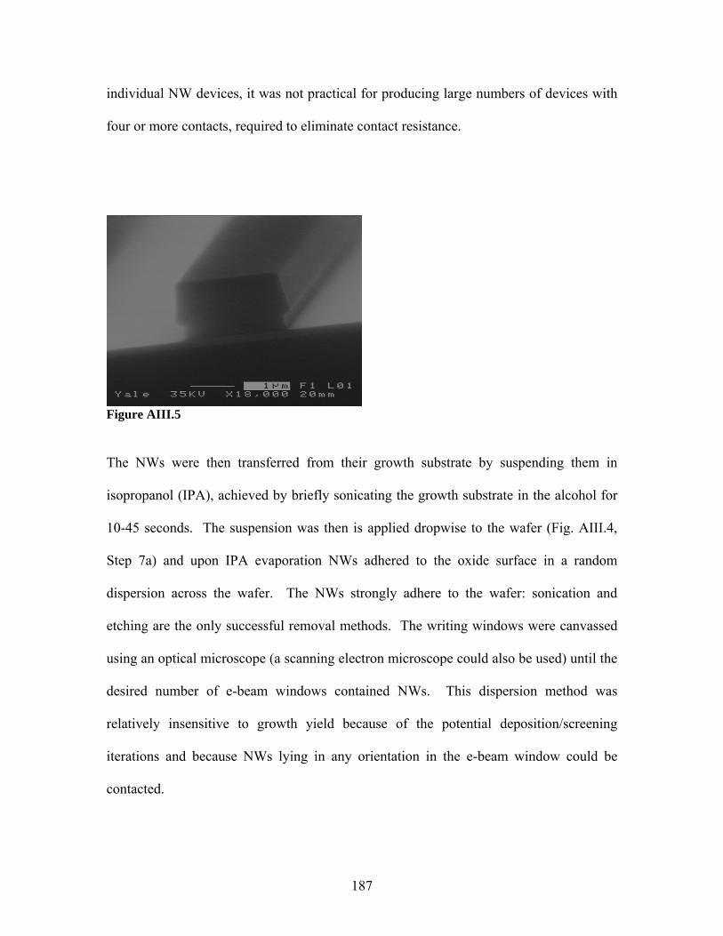
individual NW devices, it was not practical for producing large numbers of devices with
four or more contacts, required to eliminate contact resistance.
Figure AIII.5
The NWs were then transferred from their growth substrate by suspending them in
isopropanol (IPA), achieved by briefly sonicating the growth substrate in the alcohol for
10-45 seconds. The suspension was then is applied dropwise to the wafer (Fig. AIII.4,
Step 7a) and upon IPA evaporation NWs adhered to the oxide surface in a random
dispersion across the wafer. The NWs strongly adhere to the wafer: sonication and
etching are the only successful removal methods. The writing windows were canvassed
using an optical microscope (a scanning electron microscope could also be used) until the
desired number of e-beam windows contained NWs. This dispersion method was
relatively insensitive to growth yield because of the potential deposition/screening
iterations and because NWs lying in any orientation in the e-beam window could be
contacted.
187
After NW deposition, a MAA EL 13 MAA / PMMA 950 A4 bilayer was applied to the
wafer and an optical image was taken of each writing window. Alternatively, an SEM
image could be taken before resist spinning and it was found that the location of the NWs
on the wafer surface was largely unaffected by the resist spinning. Patterns were then
created to define leads to each NW device with a JEOL 6400 SEM converted to perform
direct write. The resist was exposed using typical electron doses of 350 μC/cm2, and a 1 :
3 mixture of methyl isobutyl ketone (MIBK) : IPA was used for development (Fig.
AIII.4, Step 8a). A 50 nm Ni / 300 nm Au evaporation was then performed using boiling
acetone for the liftoff (Fig. AIII.4, Step 9a).
In the optical processing method, NWs were dispersed by the technique described above
after backgate processing was completed (Fig. AIII.4, Step 5b). A subsequent optical
step was then performed to create metal contacts to the NWs that fan out to contact pads
using the LOR/photoresist bilayer described above. Photolithography was used to pattern
lines 2 or 3 microns wide spaced 2 or 3 microns apart, respectively, that run parallel for
~1 mm before fanning out to contact pads. A liftoff metallization of the contacts must be
performed because subjecting the NWs to metal etchants could be detrimental to their
properties since their stability is unknown. Furthermore, sonication cannot be used to
clean the wafers or to aid the liftoff because it may remove NWs from the wafer. Again,
a LOR/S1813 bilayer is used to create the necessary liftoff profile. A 50 nm Ni / 200 nm
Au stack was then evaporated and liftoff was performed in NMP at 60°C without
sonication, creating the contacts to the NWs (Fig. AIII.4, Step 7b). Adjacent metal leads
were electrically isolated unless linked by a NW.
188
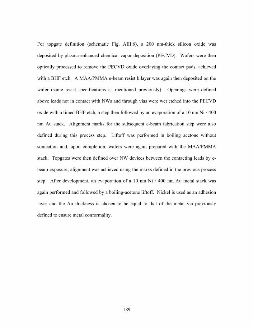
For topgate definition (schematic Fig. AIII.6), a 200 nm-thick silicon oxide was
deposited by plasma-enhanced chemical vapor deposition (PECVD). Wafers were then
optically processed to remove the PECVD oxide overlaying the contact pads, achieved
with a BHF etch. A MAA/PMMA e-beam resist bilayer was again then deposited on the
wafer (same resist specifications as mentioned previously). Openings were defined
above leads not in contact with NWs and through vias were wet etched into the PECVD
oxide with a timed BHF etch, a step then followed by an evaporation of a 10 nm Ni / 400
nm Au stack. Alignment marks for the subsequent e-beam fabrication step were also
defined during this process step. Liftoff was performed in boiling acetone without
sonication and, upon completion, wafers were again prepared with the MAA/PMMA
stack. Topgates were then defined over NW devices between the contacting leads by e-
beam exposure; alignment was achieved using the marks defined in the previous process
step. After development, an evaporation of a 10 nm Ni / 400 nm Au metal stack was
again performed and followed by a boiling-acetone liftoff. Nickel is used as an adhesion
layer and the Au thickness is chosen to be equal to that of the metal via previously
defined to ensure metal conformality.
189
Figure AIII.6
AIII.3 Device Characterization [25-29]
All electrical measurements were performed with an HP4156B Semiconductor Parameter
Analyzer (SPA). Two-point measurements were taken by varying the voltage and
measuring current; four-point measurements were taken by sweeping a current across the
outer leads and measuring the voltage across the inner leads. Two-point measurements
were taken for the inner electrodes of the 4-point contact and resistance values are
defined as the zero-bias slope [25,27,28].
Nanowire samples processed with e-beam lithography were measured on a manual
probestation with Cascade Microtech probes; for the optical process, a Cascade
Microtech Autoprobestation was used to step die-by-die and electrically screen all
190
adjacent contact leads across the entire wafer of ~150 dies for NW crossings. An Agilent
Technologies Switchbox was used to multiplex the Cascade system for the optical
process samples. Leads with Ohmic contacts to NWs were imaged with a FE-SEM to
ensure each lead pair contacted a single NW; data from lead pairs with multiple parallel
NWs are discarded [25-28].
Device transconductance was calculated by the linear best-fit to the source-drain current
(ISD) versus gate-drain voltage (V ) dependence for constant source-drain voltage (VGD SD).
The capacitance was calculated using the measured geometrical parameters. For
consistency, all NW and nanobar (NB) mobilities are calculated in the pre-saturation
regime at VSD = 1V. Thus, we calculated mobility (μ) according to Eqn. (3.1) and used
this value to determine the carrier concentration according to [25,27,28,30]
μσe
n = , (AIII.1)
where e is the elementary charge and σ is the measured conductance.
Device simulations (Silvaco) quantitatively reproduce the characteristics from the derived
mobility, show the suppression of saturation at these mobilities/densities over the
accessible source/drain voltages, and verify saturation at lower densities.
The lengths and diameters of the NWs must be known, so this data is obtained by
scanning all leads with devices of interest with a SEM. Further, during this process all
devices that are found to consist of multiple NWs are identified and discarded. Nanowire
191
diameters were approximated to the nearest 5 nm and lengths to the nearest 0.05 μm [25-
29].
AIII.4 Metal-NW Contact Characterization [26,29]
Nanowire contacts for the GaN devices fabricated as described were found to have
resistances varying over two orders of magnitude, from ~35 kΩ to ~5.4 MΩ. Four-point
measurements that eliminate contact resistance show that this wide dispersion in
resistance values is not due to the metal-semiconductor contact. We define Ohmic
contacts as devices with the best-fit-line to the ISD(VSD) plot having a correlation
coefficient R2 > 0.99 for V = -1 to 1 V. Data from seven e-beam defined devices and
from 206 optical devices is presented in this section for GaN NWs. Electron-beam
processed NW devices were found to repeatedly produce contacts with apparent Schottky
barriers of varying heights and, consequently, linear best-fits to the 2-point ISD(VSD)
characteristics of these devices routinely yield R2 < 0.975 (Fig. AIII.7). An ISD(VSD)
characteristic of a representative device is shown in the left-hand curve in the inset plot in
Fig. AIII.7. The pre-annealed and post-475°C-annealed datapoints in Fig. AIII.7 for this
device are highlighted by arrows.
192
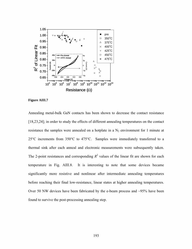
104 105 106 107 108 109 1010 1011 1012 1013
0.65
0.70
0.75
0.80
0.85
0.90
0.95
1.00
1.05
R2 o
f Lin
ear F
it
Resistance (Ω)
pre 350oC 375oC 400oC 425oC 450oC 475oC
-0.6 -0.3 0.0 0.3 0.6-40n
-20n
0
20n
40n Pre-Anneal 475oC Anneal
Voltage (V)
Cur
rent
(A)
-6µ
-3µ
0
3µ
6µ
Current (A
)
104 105 106 107 108 109 1010 1011 1012 1013
0.65
0.70
0.75
0.80
0.85
0.90
0.95
1.00
1.05
R2 o
f Lin
ear F
it
Resistance (Ω)
pre 350oC 375oC 400oC 425oC 450oC 475oC
-0.6 -0.3 0.0 0.3 0.6-40n
-20n
0
20n
40n Pre-Anneal 475oC Anneal
Voltage (V)
Cur
rent
(A)
-6µ
-3µ
0
3µ
6µ
Current (A
)
104 105 106 107 108 109 1010 1011 1012 1013
0.65
0.70
0.75
0.80
0.85
0.90
0.95
1.00
1.05
R2 o
f Lin
ear F
it
Resistance (Ω)
pre 350oC 375oC 400oC 425oC 450oC 475oC
-0.6 -0.3 0.0 0.3 0.6-40n
-20n
0
20n
40n Pre-Anneal 475oC Anneal
Voltage (V)
Cur
rent
(A)
-6µ
-3µ
0
3µ
6µ
Current (A
)
Figure AIII.7
Annealing metal-bulk GaN contacts has been shown to decrease the contact resistance
[18,23,24]; in order to study the effects of different annealing temperatures on the contact
resistance the samples were annealed on a hotplate in a N2 environment for 1 minute at
25°C increments from 350°C to 475°C. Samples were immediately transferred to a
thermal sink after each anneal and electronic measurements were subsequently taken.
The 2-point resistances and corresponding R2 values of the linear fit are shown for each
temperature in Fig. AIII.8. It is interesting to note that some devices became
significantly more resistive and nonlinear after intermediate annealing temperatures
before reaching their final low-resistance, linear states at higher annealing temperatures.
Over 50 NW devices have been fabricated by the e-beam process and ~95% have been
found to survive the post-processing annealing step.
193
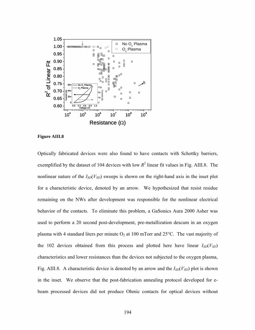
104 105 106 107 108 109
0.60
0.65
0.70
0.75
0.80
0.85
0.90
0.95
1.00
1.05
R2 o
f Lin
ear F
it
Resistance (Ω)
No O2 Plasma O
2 Plasma
0.0 0.3 0.6 0.9 1.20
20n
40n
60n No O2 Plasma O2 Plasma
Voltage (V)
Cur
rent
(A)
0
4µ
8µ
12µ
Current (A
)
104 105 106 107 108 109
0.60
0.65
0.70
0.75
0.80
0.85
0.90
0.95
1.00
1.05
R2 o
f Lin
ear F
it
Resistance (Ω)
No O2 Plasma O
2 Plasma
0.0 0.3 0.6 0.9 1.20
20n
40n
60n No O2 Plasma O2 Plasma
Voltage (V)
Cur
rent
(A)
0
4µ
8µ
12µ
Current (A
)
104 105 106 107 108 109
0.60
0.65
0.70
0.75
0.80
0.85
0.90
0.95
1.00
1.05
R2 o
f Lin
ear F
it
Resistance (Ω)
No O2 Plasma O
2 Plasma
0.0 0.3 0.6 0.9 1.20
20n
40n
60n No O2 Plasma O2 Plasma
Voltage (V)
Cur
rent
(A)
0
4µ
8µ
12µ
Current (A
)
Figure AIII.8
Optically fabricated devices were also found to have contacts with Schottky barriers,
exemplified by the dataset of 104 devices with low R2 linear fit values in Fig. AIII.8. The
nonlinear nature of the ISD(VSD) sweeps is shown on the right-hand axis in the inset plot
for a characteristic device, denoted by an arrow. We hypothesized that resist residue
remaining on the NWs after development was responsible for the nonlinear electrical
behavior of the contacts. To eliminate this problem, a GaSonics Aura 2000 Asher was
used to perform a 20 second post-development, pre-metallization descum in an oxygen
plasma with 4 standard liters per minute O2 at 100 mTorr and 25°C. The vast majority of
the 102 devices obtained from this process and plotted here have linear ISD(VSD)
characteristics and lower resistances than the devices not subjected to the oxygen plasma,
Fig. AIII.8. A characteristic device is denoted by an arrow and the ISD(VSD) plot is shown
in the inset. We observe that the post-fabrication annealing protocol developed for e-
beam processed devices did not produce Ohmic contacts for optical devices without
194
oxygen plasma treatment and often destroyed devices. Additionally, we observe that use
of an identical oxygen plasma protocol on e-beam defined samples is ineffective (e.g.
contacts are initially Schottky and require subsequent anneals in order to be made
Ohmic).
We next sought to carefully characterize the effect of metal-NW contact resistance on the
NW device behavior. Four-terminal Kelvin probe measurements were taken by varying a
current (I ) across the outer leads while measuring the voltage (V4 4) across the inner leads.
Device resistances are defined as the zero-bias slope of the inverse of the I (V4 4)
dependence. The NW resistivity is defined conventionally as
LAR NW
NW 4=ρ , (AIII.2)
where ANW is the cross-sectional NW area and L is the source-drain NW length.
All samples measured had a linear best-fit correlation coefficient R2 > 0.995. The contact
resistance, RC, of a device is determined by subtracting the 4-point resistance from the 2-
point value from the inner electrodes of the 4-point contact. The specific contact
resistivity is then defined as
CCC AR=ρ , (AIII.3)
where AC is the area of the contact, which is assumed to be half of the total NW surface
area lying under the metal lead (reasonable for e-beam evaporated films). Representative
195
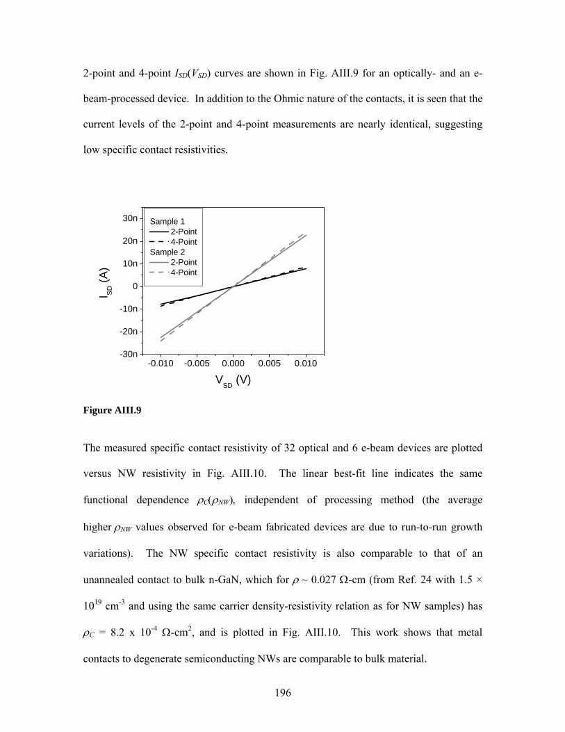
2-point and 4-point ISD(VSD) curves are shown in Fig. AIII.9 for an optically- and an e-
beam-processed device. In addition to the Ohmic nature of the contacts, it is seen that the
current levels of the 2-point and 4-point measurements are nearly identical, suggesting
low specific contact resistivities.
-0.010 -0.005 0.000 0.005 0.010-30n
-20n
-10n
0
10n
20n
30n
I SD (A
)
VSD (V)
Sample 1 2-Point 4-Point
Sample 2 2-Point 4-Point
-0.010 -0.005 0.000 0.005 0.010-30n
-20n
-10n
0
10n
20n
30n
I SD (A
)
VSD (V)
Sample 1 2-Point 4-Point
Sample 2 2-Point 4-Point
Figure AIII.9
The measured specific contact resistivity of 32 optical and 6 e-beam devices are plotted
versus NW resistivity in Fig. AIII.10. The linear best-fit line indicates the same
functional dependence ρ (ρC NW), independent of processing method (the average
higher ρNW values observed for e-beam fabricated devices are due to run-to-run growth
variations). The NW specific contact resistivity is also comparable to that of an
unannealed contact to bulk n-GaN, which for ρ ~ 0.027 Ω-cm (from Ref. 24 with 1.5 ×
1019 cm-3 and using the same carrier density-resistivity relation as for NW samples) has
ρ -4C = 8.2 x 10 Ω-cm2, and is plotted in Fig. AIII.10. This work shows that metal
contacts to degenerate semiconducting NWs are comparable to bulk material.
196
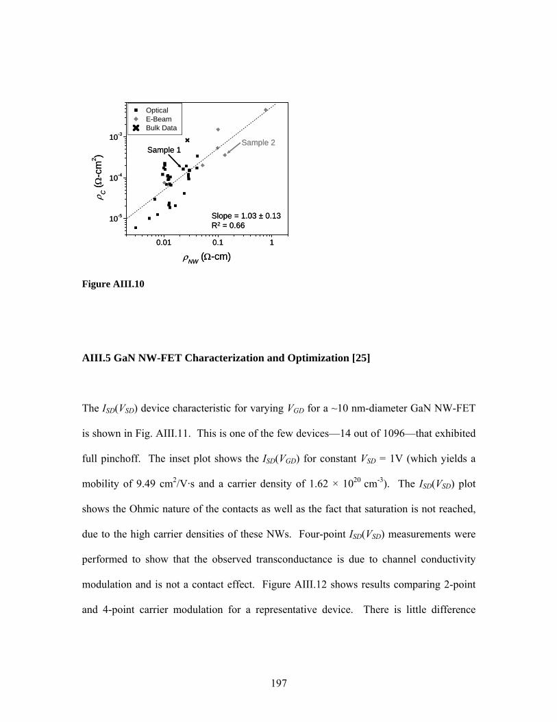
0.01 0.1 1
10-5
10-4
10-3
ρ C (Ω
-cm
2 )
ρNW (Ω-cm)
Optical E-Beam Bulk Data
Sample 1Sample 2
Slope = 1.03 ± 0.13R2 = 0.66
0.01 0.1 1
10-5
10-4
10-3
ρ C (Ω
-cm
2 )
ρNW (Ω-cm)
Optical E-Beam Bulk Data
Sample 1Sample 2
Slope = 1.03 ± 0.13R2 = 0.66
0.01 0.1 1
10-5
10-4
10-3
ρ C (Ω
-cm
2 )
ρNW (Ω-cm)
Optical E-Beam Bulk Data
Sample 1Sample 2
Slope = 1.03 ± 0.13R2 = 0.66
Figure AIII.10
AIII.5 GaN NW-FET Characterization and Optimization [25]
The ISD(VSD) device characteristic for varying VGD for a ~10 nm-diameter GaN NW-FET
is shown in Fig. AIII.11. This is one of the few devices—14 out of 1096—that exhibited
full pinchoff. The inset plot shows the ISD(V ) for constant VGD SD = 1V (which yields a
mobility of 9.49 cm2/V·s and a carrier density of 1.62 × 1020 cm-3). The ISD(VSD) plot
shows the Ohmic nature of the contacts as well as the fact that saturation is not reached,
due to the high carrier densities of these NWs. Four-point ISD(VSD) measurements were
performed to show that the observed transconductance is due to channel conductivity
modulation and is not a contact effect. Figure AIII.12 shows results comparing 2-point
and 4-point carrier modulation for a representative device. There is little difference
197
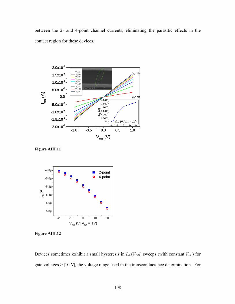
between the 2- and 4-point channel currents, eliminating the parasitic effects in the
contact region for these devices.
-1.0 -0.5 0.0 0.5 1.0-2.0x10⁻⁶
-1.5x10⁻⁶
-1.0x10⁻⁶
-5.0x10⁻⁷
0.0
5.0x10⁻⁷
1.0x10⁻⁶
1.5x10⁻⁶
2.0x10⁻⁶
I SD (A
)
VSD (V)
VG=40 VG=30 VG=20 VG=10 VG=0 VG=-10 VG=-20 VG=-30 VG=-40
-40 -20 0 20 40
0.0
3.0x10⁻⁷
6.0x10⁻⁷
9.0x10⁻⁷
1.2x10⁻⁶
1.5x10⁻⁶
1.8x10⁻⁶
VGD (V, VSD = 1V)
I SD
(A)
VG=40
VG=-40
-1.0 -0.5 0.0 0.5 1.0-2.0x10⁻⁶
-1.5x10⁻⁶
-1.0x10⁻⁶
-5.0x10⁻⁷
0.0
5.0x10⁻⁷
1.0x10⁻⁶
1.5x10⁻⁶
2.0x10⁻⁶
I SD (A
)
VSD (V)
VG=40 VG=30 VG=20 VG=10 VG=0 VG=-10 VG=-20 VG=-30 VG=-40
-40 -20 0 20 40
0.0
3.0x10⁻⁷
6.0x10⁻⁷
9.0x10⁻⁷
1.2x10⁻⁶
1.5x10⁻⁶
1.8x10⁻⁶
VGD (V, VSD = 1V)
I SD
(A)
VG=40
VG=-40
Figure AIII.11
-20 -10 0 10 20
-5.8µ
-5.6µ
-5.4µ
-5.2µ
-5.0µ
-4.8µ
I SD (A
)
VGD (V; VSD = 1V)
2-point 4-point
Figure AIII.12
Devices sometimes exhibit a small hysteresis in ISD(V ) sweeps (with constant VGD SD) for
gate voltages > |10 V|, the voltage range used in the transconductance determination. For
198
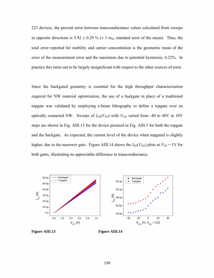
223 devices, the percent error between transconductance values calculated from sweeps
in opposite directions is 5.92 ± 0.29 % (± 1 σM, standard error of the mean). Thus, the
total error reported for mobility and carrier concentration is the geometric mean of the
error of the measurement error and the maximum due to potential hysteresis, 6.22%. In
practice this turns out to be largely insignificant with respect to the other sources of error.
Since the backgated geometry is essential for the high throughput characterization
required for NW material optimization, the use of a backgate in place of a traditional
topgate was validated by employing e-beam lithography to define a topgate over an
optically contacted NW. Sweeps of ISD(VSD) with VGD varied from -40 to 40V in 10V
steps are shown in Fig. AIII.13 for the device pictured in Fig. AIII.3 for both the topgate
and the backgate. As expected, the current level of the device when topgated is slightly
higher, due to the narrower gate. Figure AIII.14 shows the I (V ) plots at VSD GD SD = 1V for
both gates, illustrating no appreciable difference in transconductance.
0.0 0.2 0.4 0.6 0.8 1.0
0.0
10.0µ
20.0µ
30.0µ
40.0µ
50.0µ
60.0µ
I SD (A
)
VSD (V)
Backgate Topgate
-40 -20 0 20 40
54.0µ
56.0µ
58.0µ
60.0µ
62.0µ
I SD (A
)
VGD (V; VSD = 1V)
Backgate Topgate
Figure AIII.13 Figure AIII.14
199
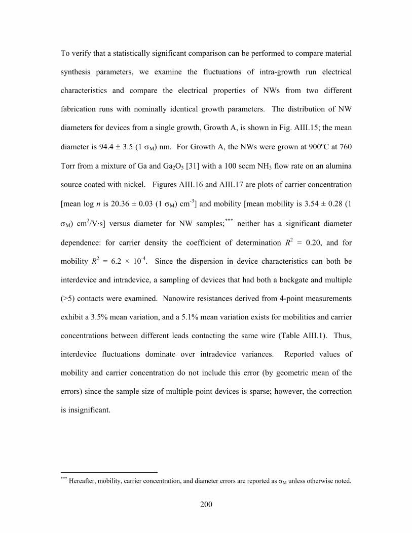
To verify that a statistically significant comparison can be performed to compare material
synthesis parameters, we examine the fluctuations of intra-growth run electrical
characteristics and compare the electrical properties of NWs from two different
fabrication runs with nominally identical growth parameters. The distribution of NW
diameters for devices from a single growth, Growth A, is shown in Fig. AIII.15; the mean
diameter is 94.4 ± 3.5 (1 σM) nm. For Growth A, the NWs were grown at 900ºC at 760
Torr from a mixture of Ga and Ga O [31] with a 100 sccm NH2 3 3 flow rate on an alumina
source coated with nickel. Figures AIII.16 and AIII.17 are plots of carrier concentration
[mean log n is 20.36 ± 0.03 (1 σM) cm-3] and mobility [mean mobility is 3.54 ± 0.28 (1
σM) cm2 ***/V·s] versus diameter for NW samples; neither has a significant diameter
dependence: for carrier density the coefficient of determination R2 = 0.20, and for
mobility R2 = 6.2 × 10⁻⁴. Since the dispersion in device characteristics can both be
interdevice and intradevice, a sampling of devices that had both a backgate and multiple
(>5) contacts were examined. Nanowire resistances derived from 4-point measurements
exhibit a 3.5% mean variation, and a 5.1% mean variation exists for mobilities and carrier
concentrations between different leads contacting the same wire (Table AIII.1). Thus,
interdevice fluctuations dominate over intradevice variances. Reported values of
mobility and carrier concentration do not include this error (by geometric mean of the
errors) since the sample size of multiple-point devices is sparse; however, the correction
is insignificant.
*** Hereafter, mobility, carrier concentration, and diameter errors are reported as σM unless otherwise noted.
200
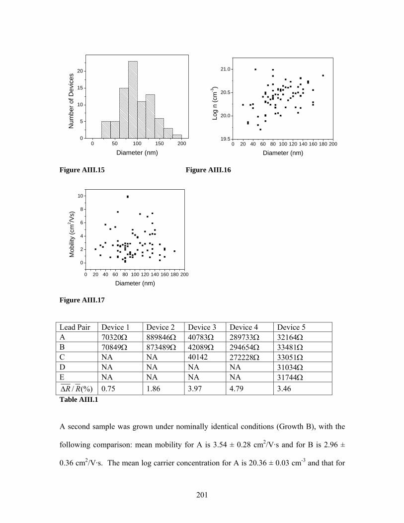
0 50 100 150 2000
5
10
15
20N
umbe
r of D
evic
es
Diameter (nm)0 20 40 60 80 100 120 140 160 180 200
19.5
20.0
20.5
21.0
Log
n (c
m-3)
Diameter (nm)
Figure AIII.15 Figure AIII.16
0 20 40 60 80 100 120 140 160 180 200
0
2
4
6
8
10
Mob
ility
(cm
2 /Vs)
Diameter (nm)
Figure AIII.17
Lead Pair Device 1 Device 2 Device 3 Device 4 Device 5 A 70320Ω 889846Ω 40783Ω 289733Ω 32164Ω B 70849Ω 873489Ω 42089Ω 294654Ω 33481Ω C NA NA 40142 272228Ω 33051Ω D NA NA NA NA 31034Ω E NA NA NA NA 31744Ω
(%)/ RRΔ 0.75 1.86 3.97 4.79 3.46 Table AIII.1
A second sample was grown under nominally identical conditions (Growth B), with the
following comparison: mean mobility for A is 3.54 ± 0.28 cm2/V·s and for B is 2.96 ±
0.36 cm2/V·s. The mean log carrier concentration for A is 20.36 ± 0.03 cm-3 and that for
201
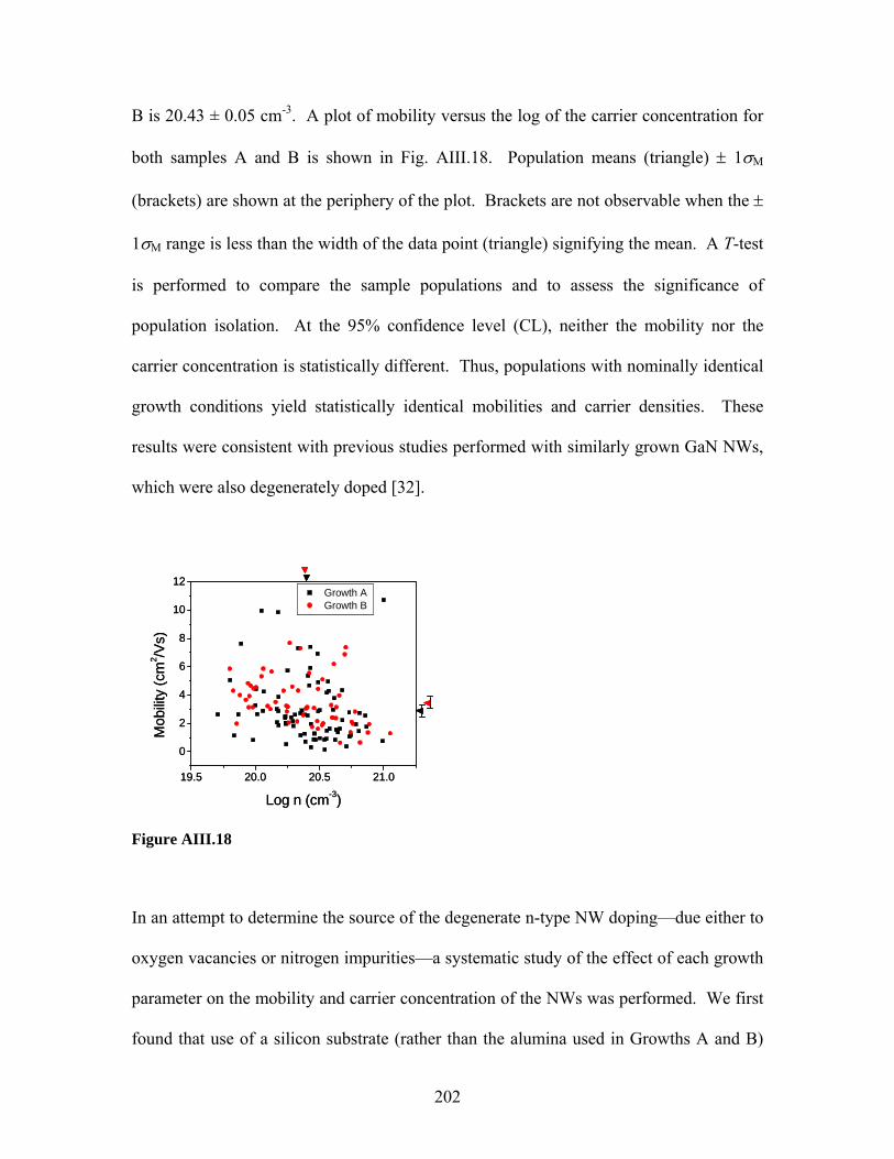
-3B is 20.43 ± 0.05 cm . A plot of mobility versus the log of the carrier concentration for
both samples A and B is shown in Fig. AIII.18. Population means (triangle) ± 1σΜ
(brackets) are shown at the periphery of the plot. Brackets are not observable when the ±
1σΜ range is less than the width of the data point (triangle) signifying the mean. A T-test
is performed to compare the sample populations and to assess the significance of
population isolation. At the 95% confidence level (CL), neither the mobility nor the
carrier concentration is statistically different. Thus, populations with nominally identical
growth conditions yield statistically identical mobilities and carrier densities. These
results were consistent with previous studies performed with similarly grown GaN NWs,
which were also degenerately doped [32].
19.5 20.0 20.5 21.0
0
2
4
6
8
10
12
Mob
ility
(cm
2 /Vs)
Log n (cm-3)
Growth A Growth B
19.5 20.0 20.5 21.0
0
2
4
6
8
10
12
Mob
ility
(cm
2 /Vs)
Log n (cm-3)
Growth A Growth B
Figure AIII.18
In an attempt to determine the source of the degenerate n-type NW doping—due either to
oxygen vacancies or nitrogen impurities—a systematic study of the effect of each growth
parameter on the mobility and carrier concentration of the NWs was performed. We first
found that use of a silicon substrate (rather than the alumina used in Growths A and B)
202
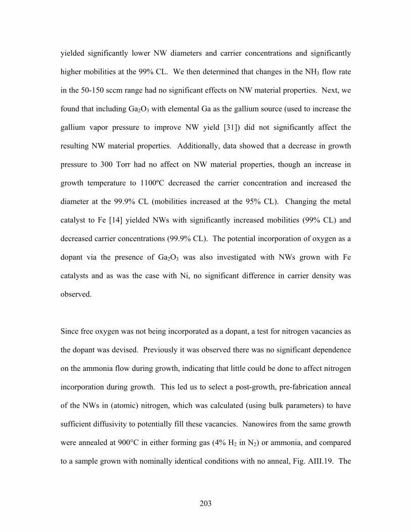
yielded significantly lower NW diameters and carrier concentrations and significantly
higher mobilities at the 99% CL. We then determined that changes in the NH3 flow rate
in the 50-150 sccm range had no significant effects on NW material properties. Next, we
found that including Ga O2 3 with elemental Ga as the gallium source (used to increase the
gallium vapor pressure to improve NW yield [31]) did not significantly affect the
resulting NW material properties. Additionally, data showed that a decrease in growth
pressure to 300 Torr had no affect on NW material properties, though an increase in
growth temperature to 1100ºC decreased the carrier concentration and increased the
diameter at the 99.9% CL (mobilities increased at the 95% CL). Changing the metal
catalyst to Fe [14] yielded NWs with significantly increased mobilities (99% CL) and
decreased carrier concentrations (99.9% CL). The potential incorporation of oxygen as a
dopant via the presence of Ga O2 3 was also investigated with NWs grown with Fe
catalysts and as was the case with Ni, no significant difference in carrier density was
observed.
Since free oxygen was not being incorporated as a dopant, a test for nitrogen vacancies as
the dopant was devised. Previously it was observed there was no significant dependence
on the ammonia flow during growth, indicating that little could be done to affect nitrogen
incorporation during growth. This led us to select a post-growth, pre-fabrication anneal
of the NWs in (atomic) nitrogen, which was calculated (using bulk parameters) to have
sufficient diffusivity to potentially fill these vacancies. Nanowires from the same growth
were annealed at 900°C in either forming gas (4% H in N2 2) or ammonia, and compared
to a sample grown with nominally identical conditions with no anneal, Fig. AIII.19. The
203
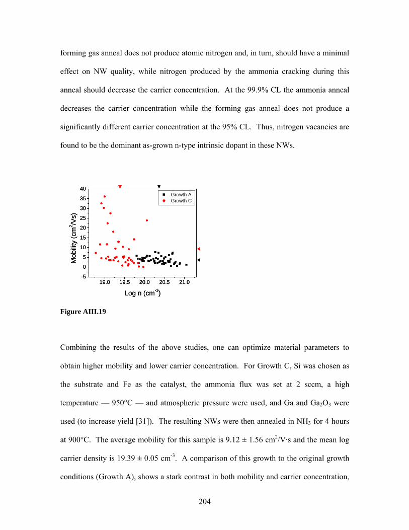
forming gas anneal does not produce atomic nitrogen and, in turn, should have a minimal
effect on NW quality, while nitrogen produced by the ammonia cracking during this
anneal should decrease the carrier concentration. At the 99.9% CL the ammonia anneal
decreases the carrier concentration while the forming gas anneal does not produce a
significantly different carrier concentration at the 95% CL. Thus, nitrogen vacancies are
found to be the dominant as-grown n-type intrinsic dopant in these NWs.
19.0 19.5 20.0 20.5 21.0-5
0
5
10
15
20
25
30
35
40
Mob
ility
(cm
2 /Vs)
Log n (cm-3)
Growth A Growth C
19.0 19.5 20.0 20.5 21.0-5
0
5
10
15
20
25
30
35
40
Mob
ility
(cm
2 /Vs)
Log n (cm-3)
Growth A Growth C
Figure AIII.19
Combining the results of the above studies, one can optimize material parameters to
obtain higher mobility and lower carrier concentration. For Growth C, Si was chosen as
the substrate and Fe as the catalyst, the ammonia flux was set at 2 sccm, a high
temperature — 950°C — and atmospheric pressure were used, and Ga and Ga2O3 were
used (to increase yield [31]). The resulting NWs were then annealed in NH3 for 4 hours
at 900°C. The average mobility for this sample is 9.12 ± 1.56 cm2/V·s and the mean log
carrier density is 19.39 ± 0.05 cm-3. A comparison of this growth to the original growth
conditions (Growth A), shows a stark contrast in both mobility and carrier concentration,
204
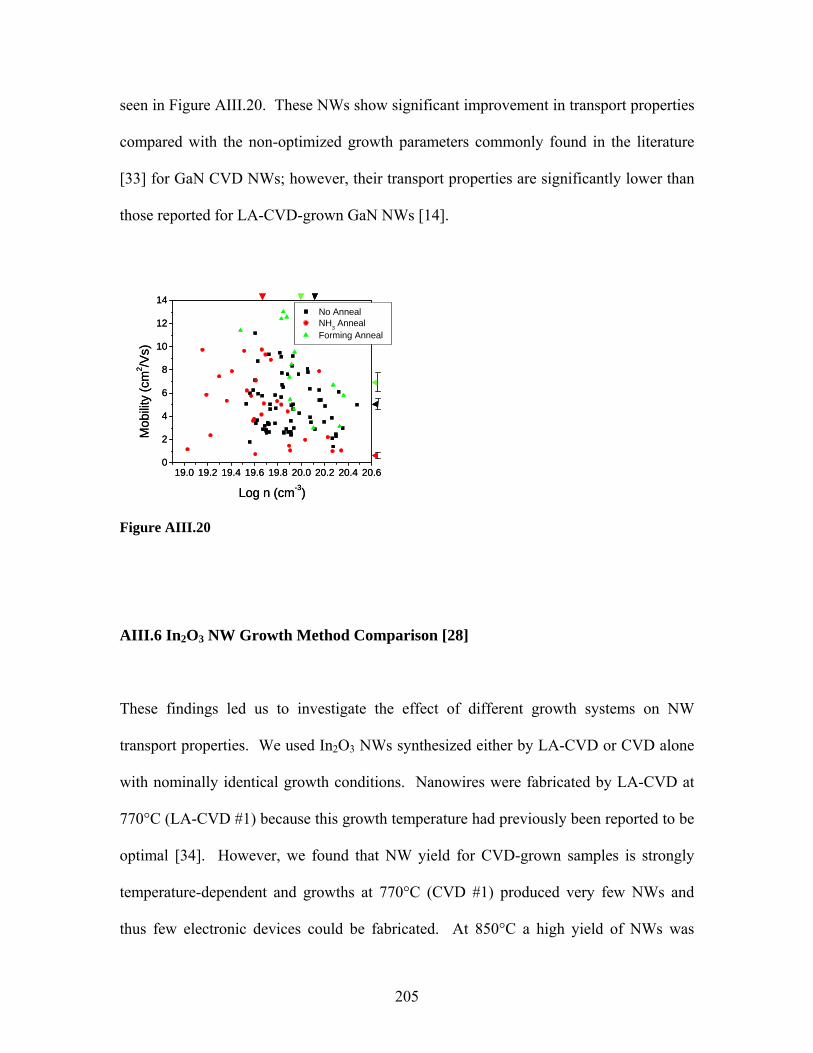
seen in Figure AIII.20. These NWs show significant improvement in transport properties
compared with the non-optimized growth parameters commonly found in the literature
[33] for GaN CVD NWs; however, their transport properties are significantly lower than
those reported for LA-CVD-grown GaN NWs [14].
19.0 19.2 19.4 19.6 19.8 20.0 20.2 20.4 20.60
2
4
6
8
10
12
14
Mob
ility
(cm
2 /Vs)
Log n (cm-3)
No Anneal NH3 Anneal Forming Anneal
19.0 19.2 19.4 19.6 19.8 20.0 20.2 20.4 20.60
2
4
6
8
10
12
14
Mob
ility
(cm
2 /Vs)
Log n (cm-3)
No Anneal NH3 Anneal Forming Anneal
Figure AIII.20
AIII.6 In O NW Growth Method Comparison [28] 2 3
These findings led us to investigate the effect of different growth systems on NW
transport properties. We used In O2 3 NWs synthesized either by LA-CVD or CVD alone
with nominally identical growth conditions. Nanowires were fabricated by LA-CVD at
770°C (LA-CVD #1) because this growth temperature had previously been reported to be
optimal [34]. However, we found that NW yield for CVD-grown samples is strongly
temperature-dependent and growths at 770°C (CVD #1) produced very few NWs and
thus few electronic devices could be fabricated. At 850°C a high yield of NWs was
205
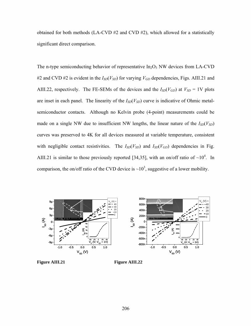
obtained for both methods (LA-CVD #2 and CVD #2), which allowed for a statistically
significant direct comparison.
OThe n-type semiconducting behavior of representative In2 3 NW devices from LA-CVD
#2 and CVD #2 is evident in the ISD(VSD) for varying VGD dependencies, Figs. AIII.21 and
AIII.22, respectively. The FE-SEMs of the devices and the ISD(V ) at VGD SD = 1V plots
are inset in each panel. The linearity of the ISD(VSD) curve is indicative of Ohmic metal-
semiconductor contacts. Although no Kelvin probe (4-point) measurements could be
made on a single NW due to insufficient NW lengths, the linear nature of the ISD(VSD)
curves was preserved to 4K for all devices measured at variable temperature, consistent
with negligible contact resistivities. The ISD(VSD) and ISD(VGD) dependencies in Fig.
AIII.21 is similar to those previously reported [34,35], with an on/off ratio of ~104. In
comparison, the on/off ratio of the CVD device is ~103, suggestive of a lower mobility.
-1.0 -0.5 0.0 0.5 1.0-800n
-600n
-400n
-200n
0
200n
400n
600n
800n
I SD (A
)
VSD (V)
VG (V) = 40 30 20 10 0
-40 -20 0 20 400
200n
400n
600n
I SD (A
)
VG (V; VSD = 1V)
-1.0 -0.5 0.0 0.5 1.0-800n
-600n
-400n
-200n
0
200n
400n
600n
800n
I SD (A
)
VSD (V)
VG (V) = 40 30 20 10 0
-40 -20 0 20 400
200n
400n
600n
I SD (A
)
VG (V; VSD = 1V)
-1.0 -0.5 0.0 0.5 1.0
-9µ
-6µ
-3µ
0
3µ
6µ
9µ
I SD (A
)
VSD (V)
VG (V) = 40 30 20 10 0
-40 -20 0 20 40
0
2µ
4µ
6µ
8µ
I SD (A
)
VG (V; VSD = 1V)
-1.0 -0.5 0.0 0.5 1.0
-9µ
-6µ
-3µ
0
3µ
6µ
9µ
I SD (A
)
VSD (V)
VG (V) = 40 30 20 10 0
-40 -20 0 20 40
0
2µ
4µ
6µ
8µ
I SD (A
)
VG (V; VSD = 1V)
Figure AIII.21 Figure AIII.22
206
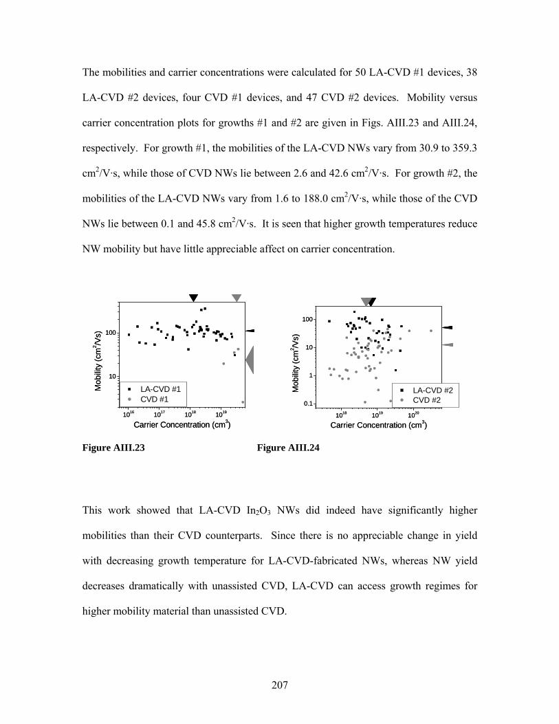
The mobilities and carrier concentrations were calculated for 50 LA-CVD #1 devices, 38
LA-CVD #2 devices, four CVD #1 devices, and 47 CVD #2 devices. Mobility versus
carrier concentration plots for growths #1 and #2 are given in Figs. AIII.23 and AIII.24,
respectively. For growth #1, the mobilities of the LA-CVD NWs vary from 30.9 to 359.3
cm2/V·s, while those of CVD NWs lie between 2.6 and 42.6 cm2/V·s. For growth #2, the
mobilities of the LA-CVD NWs vary from 1.6 to 188.0 cm2/V·s, while those of the CVD
NWs lie between 0.1 and 45.8 cm2/V·s. It is seen that higher growth temperatures reduce
NW mobility but have little appreciable affect on carrier concentration.
1016 1017 1018 1019
10
100
Mob
ility
(cm
2 /Vs)
Carrier Concentration (cm3)
LA-CVD #1 CVD #1
1016 1017 1018 1019
10
100
Mob
ility
(cm
2 /Vs)
Carrier Concentration (cm3)
LA-CVD #1 CVD #1
1018 1019 1020
0.1
1
10
100
Mob
ility
(cm
2 /Vs)
Carrier Concentration (cm3)
LA-CVD #2 CVD #2
1018 1019 1020
0.1
1
10
100
Mob
ility
(cm
2 /Vs)
Carrier Concentration (cm3)
LA-CVD #2 CVD #2
Figure AIII.23 Figure AIII.24
This work showed that LA-CVD In2O3 NWs did indeed have significantly higher
mobilities than their CVD counterparts. Since there is no appreciable change in yield
with decreasing growth temperature for LA-CVD-fabricated NWs, whereas NW yield
decreases dramatically with unassisted CVD, LA-CVD can access growth regimes for
higher mobility material than unassisted CVD.
207
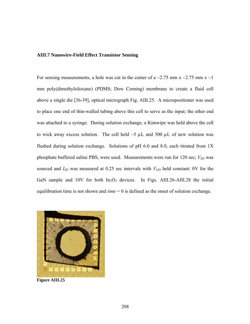
AIII.7 Nanowire-Field Effect Transistor Sensing
For sensing measurements, a hole was cut in the center of a ~2.75 mm x ~2.75 mm x ~1
mm poly(dimethylsiloxane) (PDMS; Dow Corning) membrane to create a fluid cell
above a single die [36-39], optical micrograph Fig. AIII.25. A micropositioner was used
to place one end of thin-walled tubing above this cell to serve as the input; the other end
was attached to a syringe. During solution exchange, a Kimwipe was held above the cell
to wick away excess solution. The cell held ~5 μL and 500 μL of new solution was
flushed during solution exchange. Solutions of pH 6.0 and 8.0, each titrated from 1X
phosphate buffered saline PBS, were used. Measurements were run for 120 sec; VSD was
sourced and ISD was measured at 0.25 sec intervals with VGD held constant: 0V for the
GaN sample and 10V for both In O2 3 devices. In Figs. AIII.26-AIII.28 the initial
equilibration time is not shown and time = 0 is defined as the onset of solution exchange.
Figure AIII.25
208
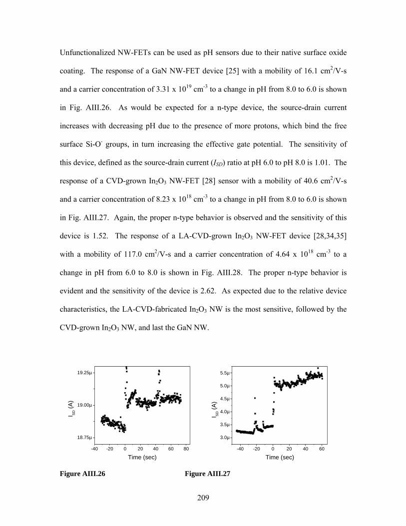
Unfunctionalized NW-FETs can be used as pH sensors due to their native surface oxide
coating. The response of a GaN NW-FET device [25] with a mobility of 16.1 cm2/V-s
and a carrier concentration of 3.31 x 1019 cm-3 to a change in pH from 8.0 to 6.0 is shown
in Fig. AIII.26. As would be expected for a n-type device, the source-drain current
increases with decreasing pH due to the presence of more protons, which bind the free
surface Si-O- groups, in turn increasing the effective gate potential. The sensitivity of
this device, defined as the source-drain current (ISD) ratio at pH 6.0 to pH 8.0 is 1.01. The
response of a CVD-grown In2O3 NW-FET [28] sensor with a mobility of 40.6 cm2/V-s
and a carrier concentration of 8.23 x 1018 cm-3 to a change in pH from 8.0 to 6.0 is shown
in Fig. AIII.27. Again, the proper n-type behavior is observed and the sensitivity of this
device is 1.52. The response of a LA-CVD-grown In O NW-FET device [28,34,352 3 ]
with a mobility of 117.0 cm2 18/V-s and a carrier concentration of 4.64 x 10 cm-3 to a
change in pH from 6.0 to 8.0 is shown in Fig. AIII.28. The proper n-type behavior is
evident and the sensitivity of the device is 2.62. As expected due to the relative device
characteristics, the LA-CVD-fabricated In2O3 NW is the most sensitive, followed by the
CVD-grown In2O NW, and last the GaN NW. 3
-40 -20 0 20 40 60 80
18.75µ
19.00µ
19.25µ
I SD (A
)
Time (sec)-40 -20 0 20 40 60
3.0µ
3.5µ
4.0µ
4.5µ
5.0µ
5.5µ
I SD (A
)
Time (sec)
Figure AIII.26 Figure AIII.27
209
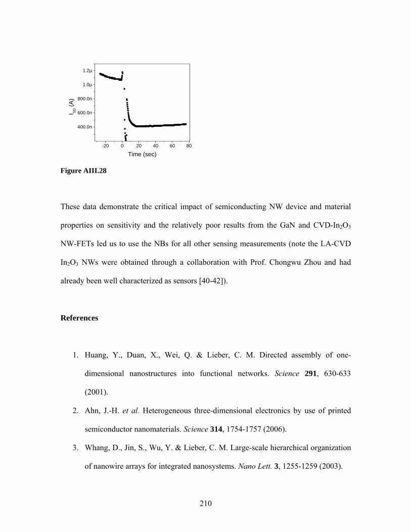
-20 0 20 40 60 80
400.0n
600.0n
800.0n
1.0µ
1.2µI S
D (A
)
Time (sec)
Figure AIII.28
These data demonstrate the critical impact of semiconducting NW device and material
properties on sensitivity and the relatively poor results from the GaN and CVD-In O2 3
NW-FETs led us to use the NBs for all other sensing measurements (note the LA-CVD
In2O3 NWs were obtained through a collaboration with Prof. Chongwu Zhou and had
already been well characterized as sensors [40-42]).
References
1. Huang, Y., Duan, X., Wei, Q. & Lieber, C. M. Directed assembly of one-
dimensional nanostructures into functional networks. Science 291, 630-633
(2001).
2. Ahn, J.-H. et al. Heterogeneous three-dimensional electronics by use of printed
semiconductor nanomaterials. Science 314, 1754-1757 (2006).
3. Whang, D., Jin, S., Wu, Y. & Lieber, C. M. Large-scale hierarchical organization
of nanowire arrays for integrated nanosystems. Nano Lett. 3, 1255-1259 (2003).
210
4. Englander, O., Christensen, D., Kim, J., Lin, L. & Morris, S. J. S. Electric-field
assisted growth and self-assembly of intrinsic silicon nanowires. Nano Lett. 5,
705-708 (2005).
5. Goldberger, J., Hochbaum, A. I., Fan, R. & Yang, P. Silicon vertically integrated
nanowire field effect transistors. Nano Lett. 6, 973-977 (2006).
6. Wen, J. G. et al. Self-assembly of semiconducting oxide nanowires, nanorods,
and nanoribbons. Chem. Phys. Lett. 372, 717-722 (2003).
7. Hopkins, D. S., Pekker, D., Goldbart, P. M. & Bezryadin, A. Quantum
interference device made by DNA templating of superconducting nanowires.
Science 308, 1762-1765 (2005).
8. Sirbuly, D. J. et al. Optical routing and sensing with nanowire assemblies. Proc.
Natl. Acad. Sci. U.S.A. 102, 7800-7805 (2005).
9. Mao, C. et al. Viral assembly of oriented quantum dot nanowires. Proc. Natl.
Acad. Sci. U.S.A. 100, 6946-6951 (2003).
10. Walter, E. C. et al. Metal nanowire arrays by electrodeposition. ChemPhysChem
4, 131-138 (2003).
11. Martensson, T. et al. Nanowire arrays defined by nanoimprint lithography. Nano
Lett. 4, 699-702 (2004).
12. Evoy, S. et al. Dielectrophoretic assembly and integration of nanowire devices
with functional CMOS operating circuitry. Microelec. Eng. 75, 31-42 (2004).
13. Cui, Y. et al. High performance silicon nanowire field effect transistors. Nano
Lett. 3, 149-152 (2003).
211
14. Huang, Y., Duan, X., Cui, Y. & Lieber, C. M. Gallium nitride nanowire
nanodevices. Nano Lett. 2, 101-104 (2002).
15. Cui, Y., Wei, Q., Park, H. & Lieber, C. M. Nanowire nanosensors for highly
sensitive and selective detection of biological and chemical species. Science 293,
1289-1292 (2001).
16. Duan, X., Huang, Y., Cui, Y., Wang, J. & Lieber, C. M. Indium phosphide
nanowires as building blocks for nanoscale electronic and optoelectronic devices.
Nature 409, 66-69 (2001).
17. Chung, S.-W., Yu, J.-Y. & Heath, J. R. Silicon nanowire devices. Appl. Phys.
Lett. 76, 2068-2070 (2000).
18. Cheng, G. et al. Current rectification in a single GaN nanowire with a well-
defined p-n junction. Appl. Phys. Lett. 83, 1578-1580 (2003).
19. Wang, D., Lu, J.G., Otten, C. J. & Buhro, W. E. Electrical transport in boron
nanowires. Appl. Phys. Lett. 83, 5280-5282 (2003).
20. De Franceschi, S. et al. Single-electron tunneling in InP nanowires. Appl. Phys.
Lett. 83, 344-346 (2003).
21. Cui, Y., Duan, X., Hu, J. & Lieber, C. M. Doping and electrical transport in
silicon nanowires. J. Phys. Chem. B 104, 5213-5216 (2000).
22. Kim, J.-R. et al. Schottky diodes based on a single GaN nanowire. Nanotech. 13,
701-704 (2002).
23. Hwang, J. S. et al. Effect of Ti thickness on contact resistance between GaN
nanowires and Ti/Au electrodes. Appl. Phys. Lett. 85, 1636-1638 (2004).
212
24. Pal, S. & Sugino, T. Fabrication and characterization of metal/GaN contacts.
Appl. Surf. Sci. 161, 263-267 (2000).
25. Stern, E. et al. Electrical characterization of single GaN nanowires. Nanotech. 16,
2941-2953 (2005).
26. Stern, E. et al. Methods for fabricating Ohmic contacts to nanowires and
nanotubes. J. Vac. Sci. Technol. B 24, 231-236 (2006).
27. Cheng, G., Stern, E., Turner-Evans, D. & Reed, M. A. Electronic properties of
InN nanowires. Appl. Phys. Lett. 87, Art. No. 253103 (2005).
28. Stern, E. et al. Comparison of laser-ablation and hot-wall chemical vapor
deposition techniques for nanowire fabrication. Nanotech. 17, S246-S252 (2006).
29. Stern, E., Cheng, G., Young, M. P. & Reed, M. A. Specific contact resistivity of
nanowire devices. Appl. Phys. Lett. 88, Art. No. 053106 (2006).
30. Sze, S. M. Physics of Semiconductor Devices 2nd Edn. (John Wiley & Sons, New
York, 1981).
31. Shi, W., Zheng, Y., Wang, N., Lee, C.-S. & Lee, S.-T. A general synthetic route
to III-V compound semiconductor nanowires. Adv. Mater. 13, 591-594 (2001).
32. Kim, J.-R. et al. Temperature-dependent single-electron tunneling effect in lightly
and heavily doped GaN nanowires. Phys. Rev. B 69, Art. No. 233303 (2004).
33. Kim, J.-R. et al. Electrical transport properties of individual gallium nitride
nanowires synthesized by chemical-vapor-deposition. Appl. Phys. Lett. 80, 3548-
3550 (2002).
34. Li, C. et al. Diameter-controlled growth of single-crystalline In2O3 nanowires and
their electronic properties. Adv. Mater.15, 143-146 (2003).
213
35. Lei, B., Li, C., Zhang, D. & Zhou, C. Tuning electronic properties of In O2 3
nanowires by doping control. Appl. Phys. A 79, 439-442 (2004).
36. Stern, E. et al. Electropolymerization on microelectrodes: functionalization
technique for selective protein and DNA conjugation. Anal. Chem. 78, 6340-6346
(2006).
37. Duffy, D. C., McDonald, J. C., Schueller, O. J. A. & Whitesides, G. M. Rapid
prototyping of microfluidic systems in poly(dimethylsiloxane). Anal. Chem. 70,
4974-4984 (1998).
38. Li, X., Klemic, K. G., Reed, M. A. & Sigworth, F. J. Microfluidic system for
planar patch clamp electrode arrays. Nano Lett. 6, 815-819 (2006).
39. Whitesides, G. M. et al. Soft lithography in biology and biochemistry. Annu. Rev.
Biomed. Eng. 3, 335-373 (2001).
40. Tang, T. et al. Complementary response of In O2 3 nanowires and carbon nanotubes
to low-density lipoprotein chemical gating. Appl. Phys. Lett. 86, Art. No. 103903
(2005).
41. Li, C. et al. Complementary detection of prostate-specific antigen using In O2 3
nanowires and carbon nanotubes. J. Am. Chem. Soc. 127, 12484-12485 (2005).
42. Rouhanizadeh, M. et al. Differentiation of oxidized low density lipoproteins by
nanosensors. Sens. Act. B 114, 788-798 (2006).
214


![119 Nanowires 4. Nanowires - UFAMhome.ufam.edu.br/berti/nanomateriais/Nanowires.pdf · 119 Nanowires 4. Nanowires ... written about carbon nanotubes [4.57–59], which can be](https://img.pdfslide.us/doc/110x75/5abfd11e7f8b9a5d718eba2b/119-nanowires-4-nanowires-nanowires-4-nanowires-written-about-carbon-nanotubes.jpg)