Embed Size (px)
Citation preview
Laurens W. Molenkamp
Physikalisches Institut, EP3Universität Würzburg
Overview
- HgTe/CdTe bandstructure, quantum spin Hall effect- Dirac surface states of strained bulk HgTe- Josephson junctions and SQUIDs

5.1 5.2 5.3 5.4 5.5 5.6 5.7 5.8 5.9 6.0 6.1 6.2 6.3 6.4 6.5 6.76.6
1.0
1.5
0.5
0.0
-0.5
2.0
2.5
3.0
3.5
4.0
4.5
5.0
6.0
5.5
Bandgap vs. lattice constant(at room temperature in zinc blende structure)
Ban
dgap
ene
rgy
(eV
)
lattice constant a [Å]0 © CT-CREW 1999
MBE-Growth
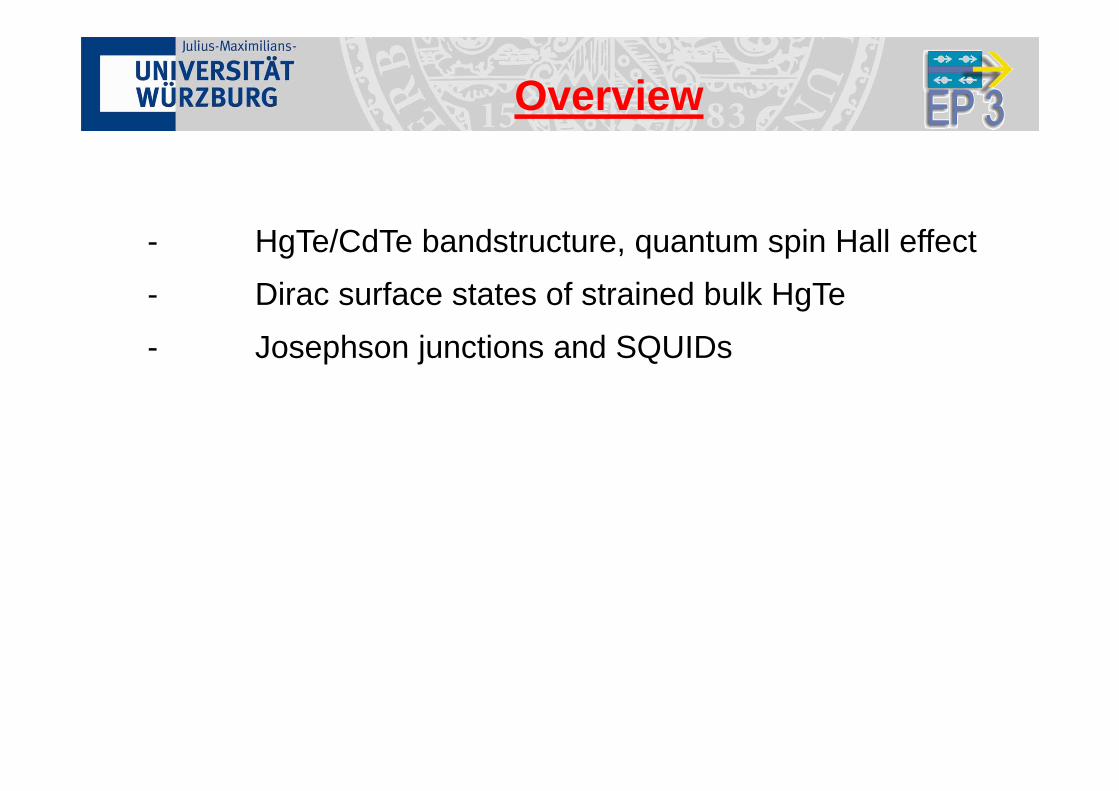
HgTe-Quantum Wells

band structure
D.J. Chadi et al. PRB, 3058 (1972)
fundamental energy gap
meV 30086 EE meV 30086 EE
semi-metal or semiconductor
HgTe
-1.0 -0.5 0.0 0.5 1.0k (0.01 )
-1500
-1000
-500
0
500
1000
E(m
eV) 8
6
7
-1.0 -0.5 0.0 0.5 1.0k (0.01 )
-1500
-1000
-500
0
500
1000
E(m
eV) 8
6
7
Eg
-1.0 -0.5 0.0 0.5 1.0k (0.01 )
-1500
-1000
-500
0
500
1000
E(m
eV)
HgTe
8
6
7
-1.0 -0.5 0.0 0.5 1.0k (0.01 )
Hg0.32Cd0.68Te
-1500
-1000
-500
0
500
1000
E(m
eV)
6
8
7
VBO
-1.0 -0.5 0.0 0.5 1.0k (0.01 )
-1500
-1000
-500
0
500
1000
E(m
eV)
HgTe
8
6
7
-1.0 -0.5 0.0 0.5 1.0k (0.01 )
Hg0.32Cd0.68Te
-1500
-1000
-500
0
500
1000
E(m
eV)
6
8
7
VBO
BarrierQW
VBO = 570 meV
HgTe-Quantum Wells
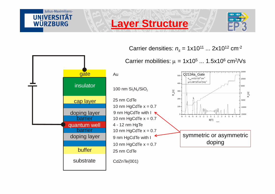
Layer Structure
gate
insulator
cap layer
doping layer
barrier
barrierquantum well
doping layer
buffer
substrate
Au
100 nm Si N /SiO
3 4 2
25 nm CdTe
CdZnTe(001)
25 nm CdTe10 nm HgCdTe x = 0.79 nm HgCdTe with I10 nm HgCdTe x = 0.74 - 12 nm HgTe10 nm HgCdTe x = 0.7 9 nm HgCdTe with I10 nm HgCdTe x = 0.7
symmetric or asymmetricdoping
Carrier densities: ns = 1x10¹¹ ... 2x1012 cm-2
Carrier mobilities: = 1x10⁵ ... 1.5x106 cm2/Vs
-8 -7 -6 -5 -4 -3 -2 -1 0 1 2 3 4 5 6 7 80
100
200
300
400
500
µ=1.06*106cm2(Vs)-1
nHall=4.01*1011cm-2
Q2134a_Gate
B[T]
Rxx
[]
-15000
-10000
-5000
0
5000
10000
15000
Graph2
Rxy
[]
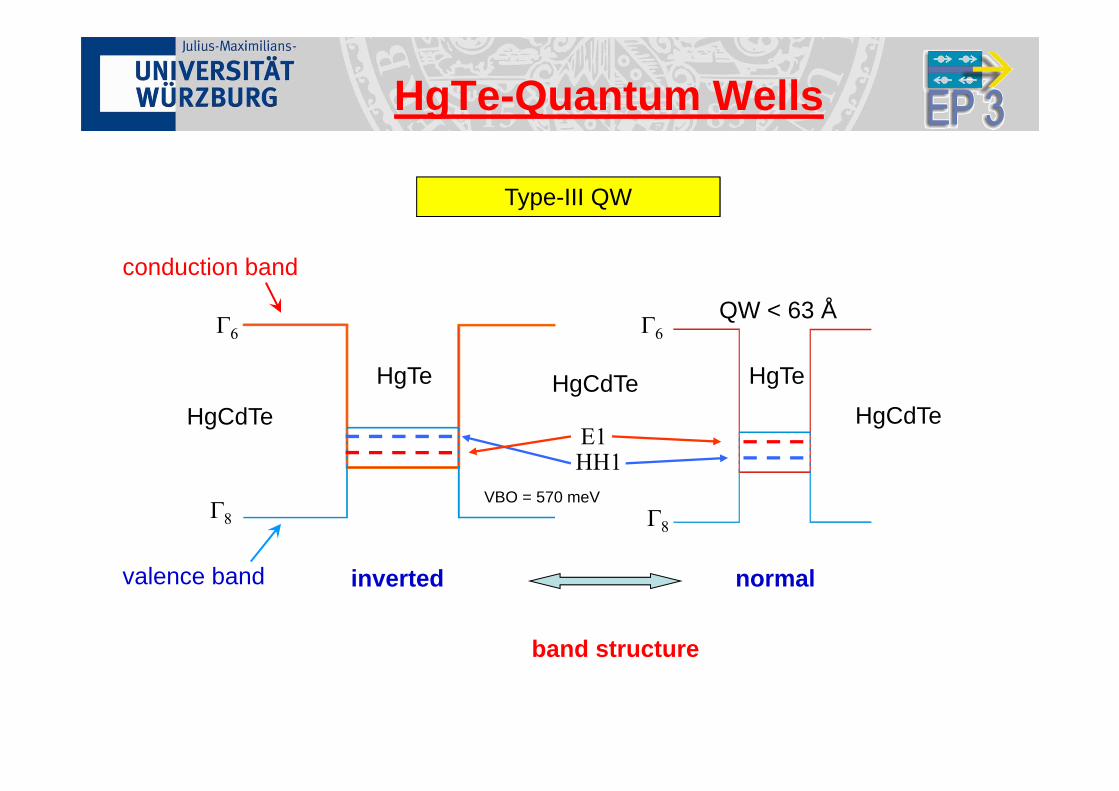
Type-III QW
VBO = 570 meV
HgCdTeHgCdTeHgTe
HgCdTe
HH1E1
QW < 63 Å
HgTe
inverted normal
band structure
conduction band
valence band
HgTe-Quantum Wells
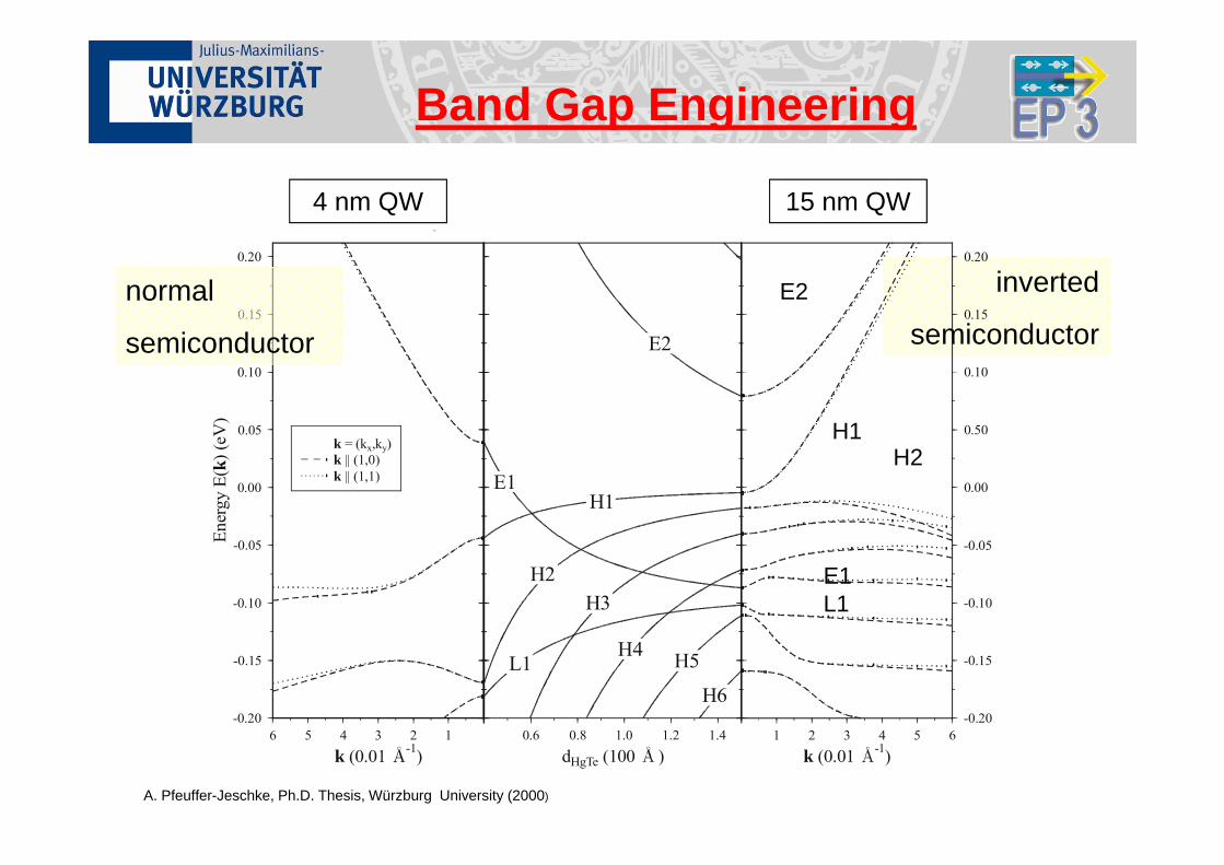
123456
k (0.01 -1)
-0.20
-0.15
-0.10
-0.05
0.00
0.05
0.10
0.15
0.20
Ener
gyE(
k)(e
V)
k || (1,1)k || (1,0)k = (kx,ky)
k || (1,1)k || (1,0)k = (kx,ky)
4 nm QW 15 nm QW
normal
semiconductor
inverted
semiconductor
1 2 3 4 5 6
k (0.01 -1)
-0.20
-0.15
-0.10
-0.05
0.00
0.50
0.10
0.15
0.20
E2
H1H2
E1L1
0.6 0.8 1.0 1.2 1.4
dHgTe (100 )
E2E2
E1E1H1H1
H2H2H3H3
H4H4 H5H5
H6H6L1L1
Band Gap Engineering
A. Pfeuffer-Jeschke, Ph.D. Thesis, Würzburg University (2000)

Bandstructure HgTe
E
k
E1
H1
invertedgap
4.0nm 6.2 nm 7.0 nm
normalgap
H1
E1
B.A Bernevig, T.L. Hughes, S.C. Zhang, Science 314, 1757 (2006)

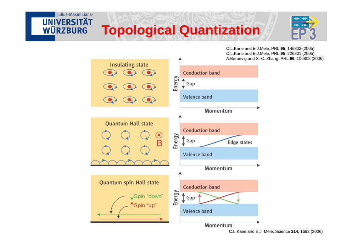
Topological Quantization
C.L.Kane and E.J. Mele, Science 314, 1692 (2006)
C.L.Kane and E.J.Mele, PRL 95, 146802 (2005)C.L.Kane and E.J.Mele, PRL 95, 226801 (2005)A.Bernevig and S.-C. Zhang, PRL 96, 106802 (2006)
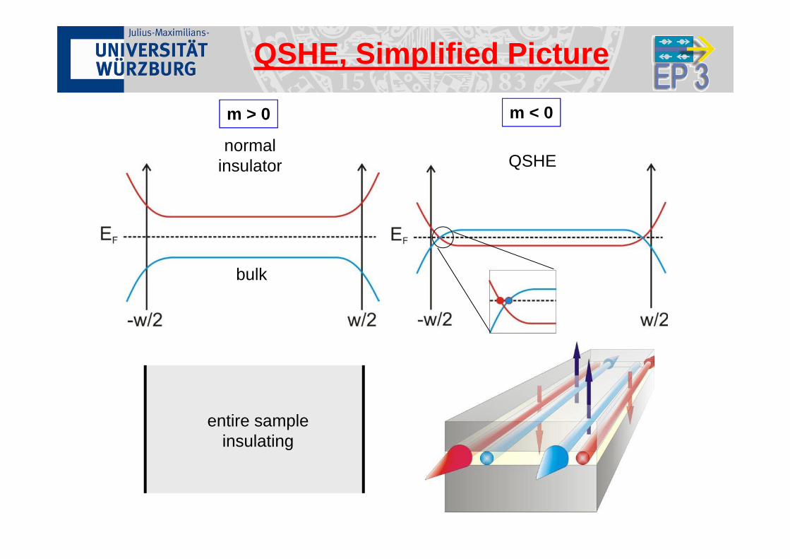
QSHE, Simplified Picture
normalinsulator
bulk
bulkinsulating
entire sampleinsulating
m > 0 m < 0
QSHE
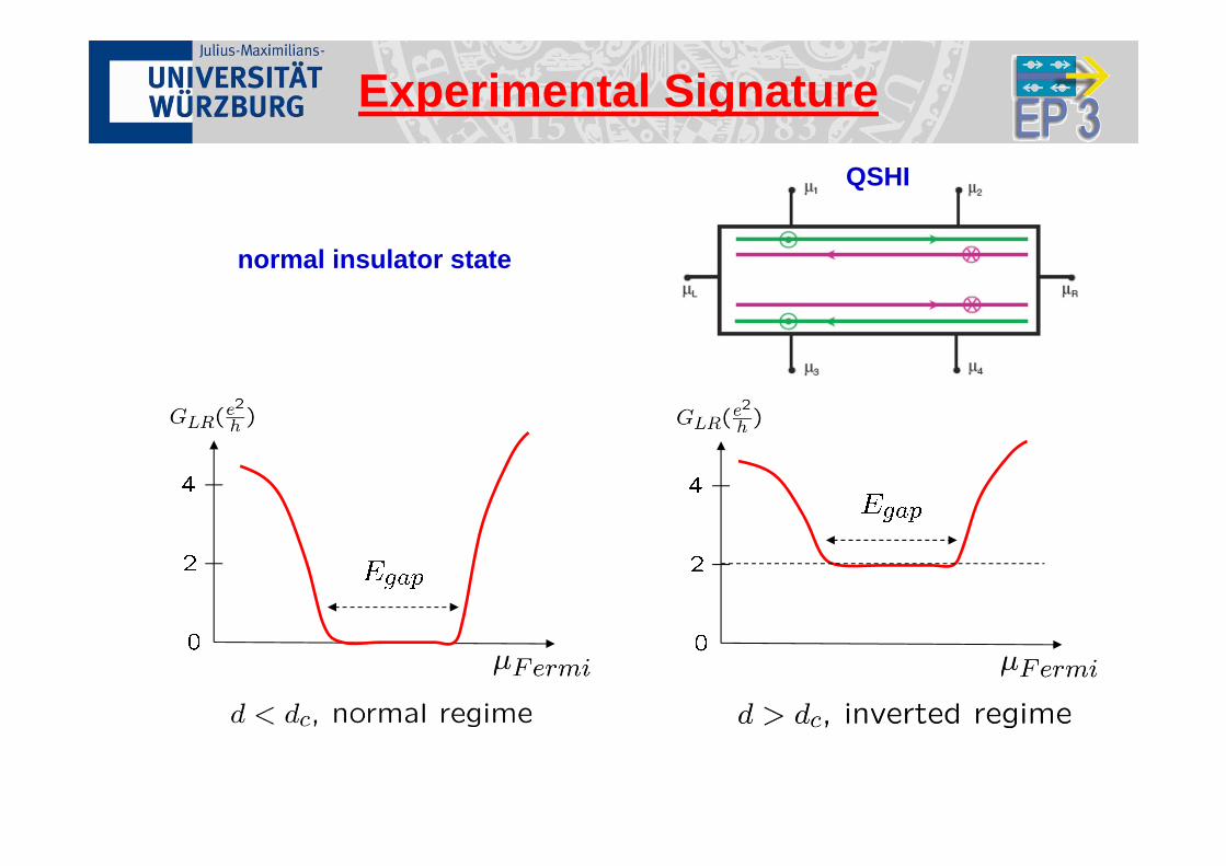
Experimental Signature
normal insulator state
QSHI
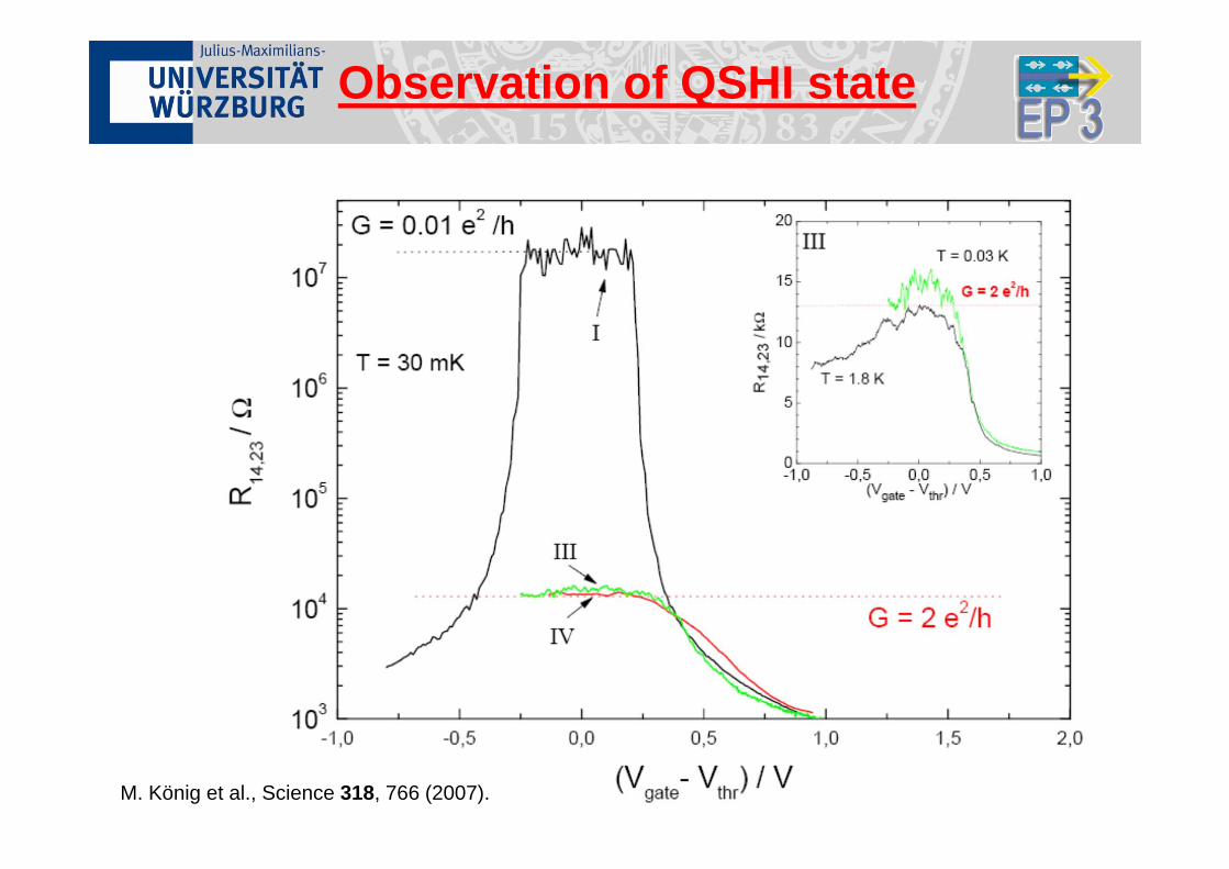
Observation of QSHI state
M. König et al., Science 318, 766 (2007).
-1.0 -0.5 0.0 0.5 1.0 1.5 2.0103
104
105
106
G = 2 e2/h
Rxx
/
(VGate- Vthr) / V
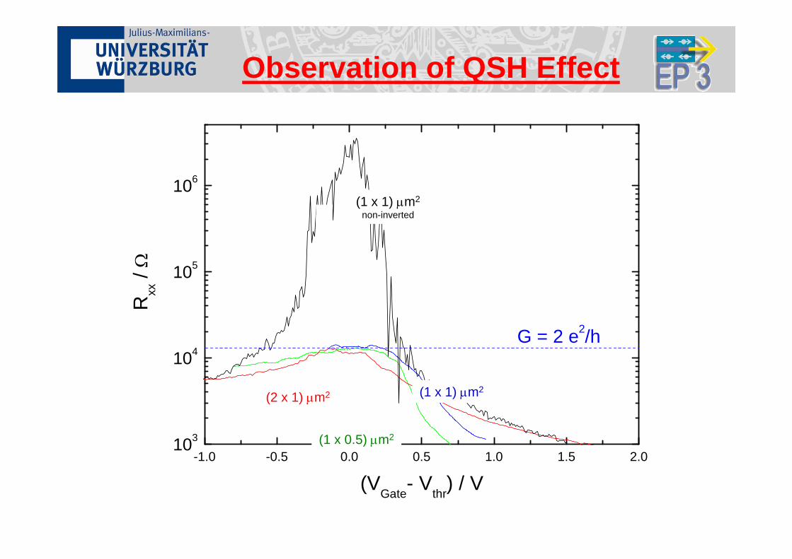
Observation of QSH Effect
(1 x 0.5) m2
(1 x 1) m2(2 x 1) m2
(1 x 1) m2
non-inverted
1 m 2 m
1 2 3
6 5 4
1 m
1 m
5 m
1 2
34
(a) (b)
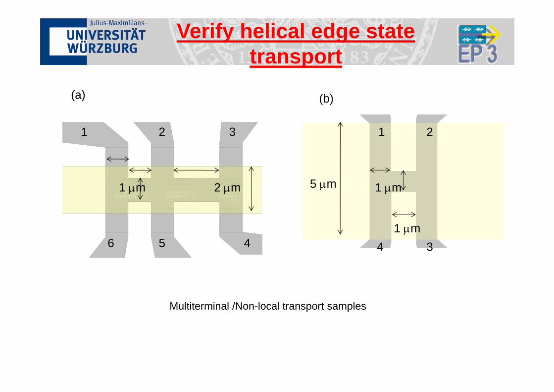
Verify helical edge state transport
Multiterminal /Non-local transport samples
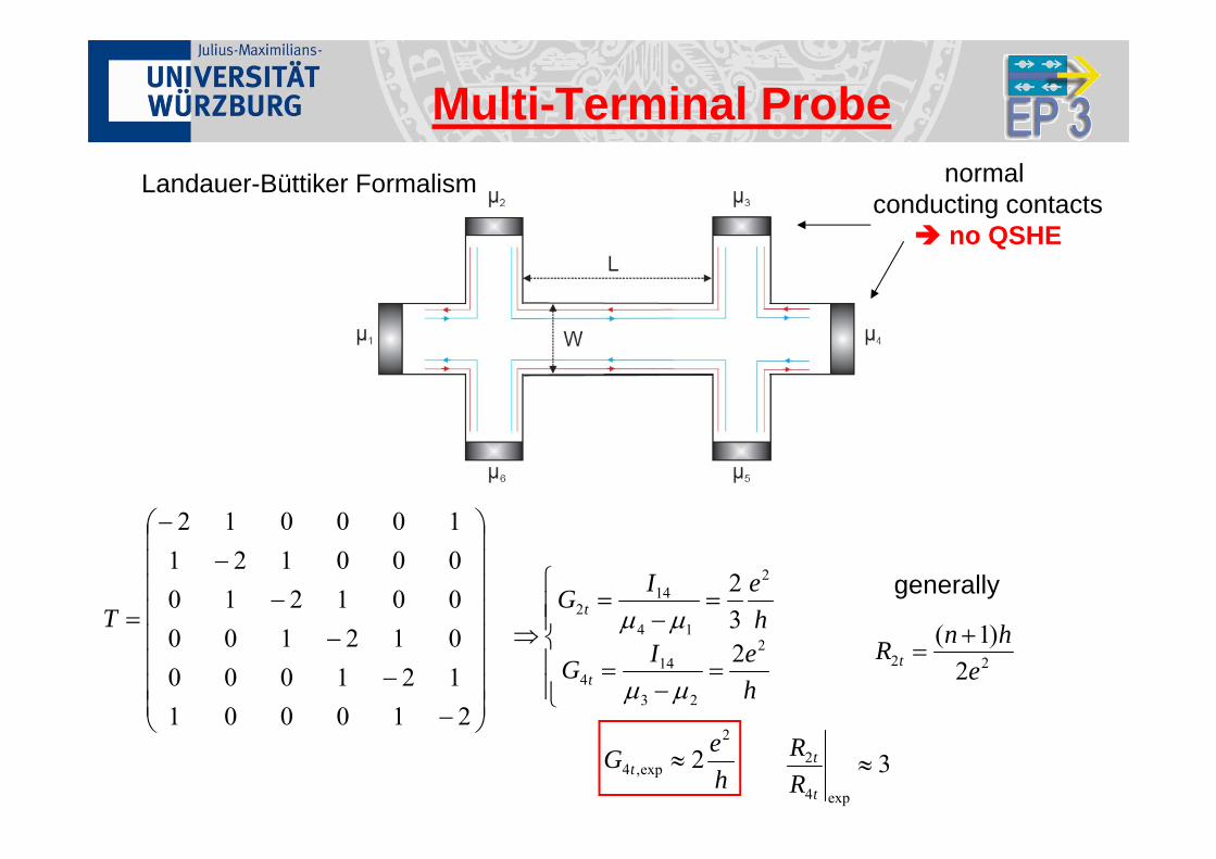
Multi-Terminal Probe
210001121000012100001210000121100012
T
heIG
heIG
t
t
2
23
144
2
14
142
232
generally
22 2)1(
ehnR t
3exp4
2 t
t
RR
heG t
2
exp,4 2
Landauer-Büttiker Formalism normal conducting contacts no QSHE

0.0 0.5 1.0 1.5 2.00
5
10
15
20
25
R (k
)
V* (V)
I: 1-4V: 2-3
1
3
2
4
R14,23=1/4 h/e2
R14,14=3/4 h/e2
Non-Local data on H-bar
A. Roth et al., Science 325, 294 (2009).
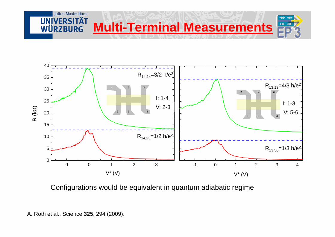
Configurations would be equivalent in quantum adiabatic regime
-1 0 1 2 30
5
10
15
20
25
30
35
40
R (k
)
V* (V)
I: 1-4V: 2-3
R14,23=1/2 h/e2
R14,14=3/2 h/e2
I: 1-3V: 5-6
R13,13=4/3 h/e2
R13,56=1/3 h/e2
-1 0 1 2 3 4
V* (V)
Multi-Terminal Measurements
A. Roth et al., Science 325, 294 (2009).
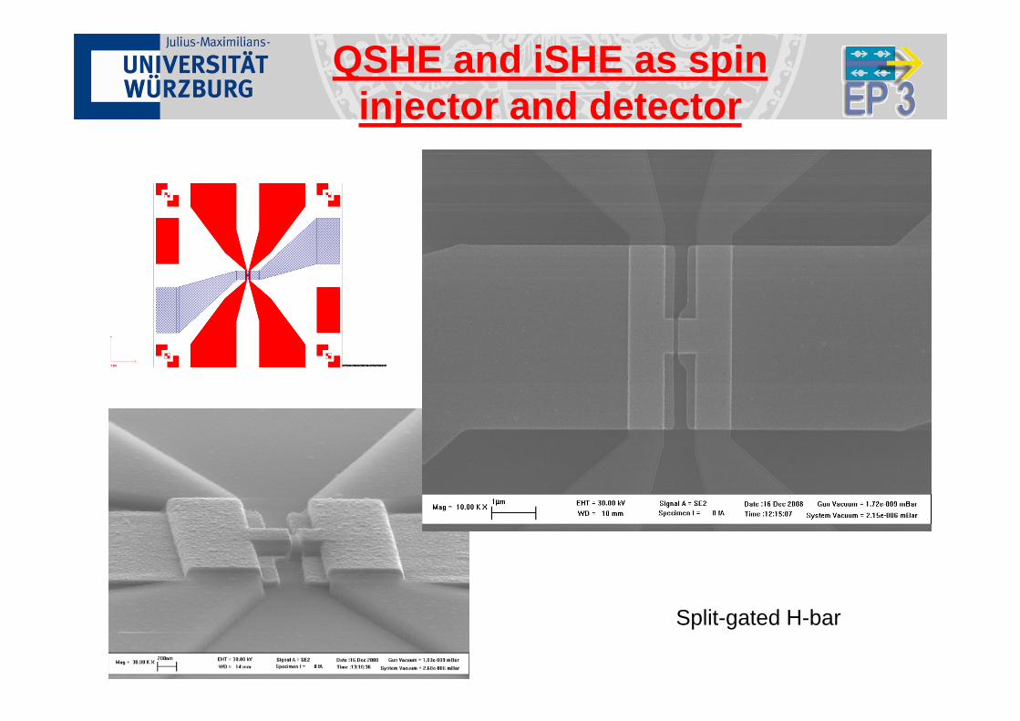
QSHE and iSHE as spin injector and detector
Split-gated H-bar

Detect iSHE through QSHI edge channels
I
U
Gate in 3-8 leg is scanned, 2-9 leg is n-type metallic,
current passed between contacts 2 and 9.
C. Brüne et al., Nature Physics 8, 486–491 (2012)

Detect QSHI throughinverse iSHE
I
U
Gate in 3-8 leg is scanned, 2-9 leg is n-type metallic,
current passed between contacts 3 and 8 C. Brüne et al., Nature Physics 8, 486–491 (2012).

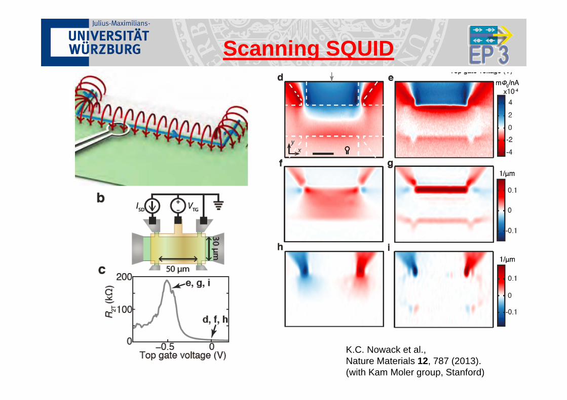
Scanning SQUID
K.C. Nowack et al., Nature Materials 12, 787 (2013).(with Kam Moler group, Stanford)


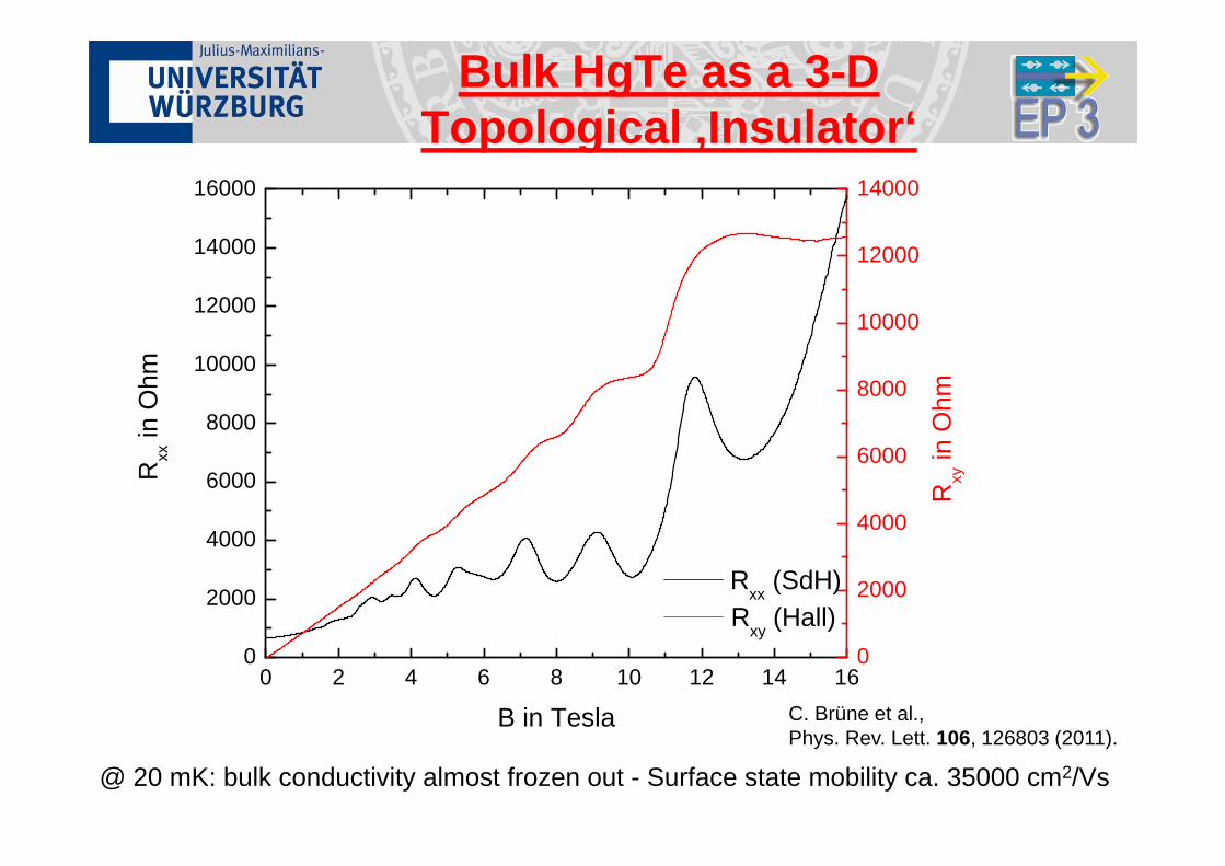
Bulk HgTe as a 3-D Topological ‚Insulator‘
-1.0 -0.5 0.0 0.5 1.0k (0.01 )
-1500
-1000
-500
0
500
1000
E(m
eV) 8
6
7
-1.0 -0.5 0.0 0.5 1.0k (0.01 )
-1500
-1000
-500
0
500
1000
E(m
eV) 8
6
7
Bulk HgTe is semimetal,
topological surface state overlaps w/ valenceband.
k(1/a)
E-E
F(eV
)
ARPES: Yulin Chen, ZX Shen,
StanfordC. Brüne et al., Phys. Rev. Lett. 106, 126803 (2011).
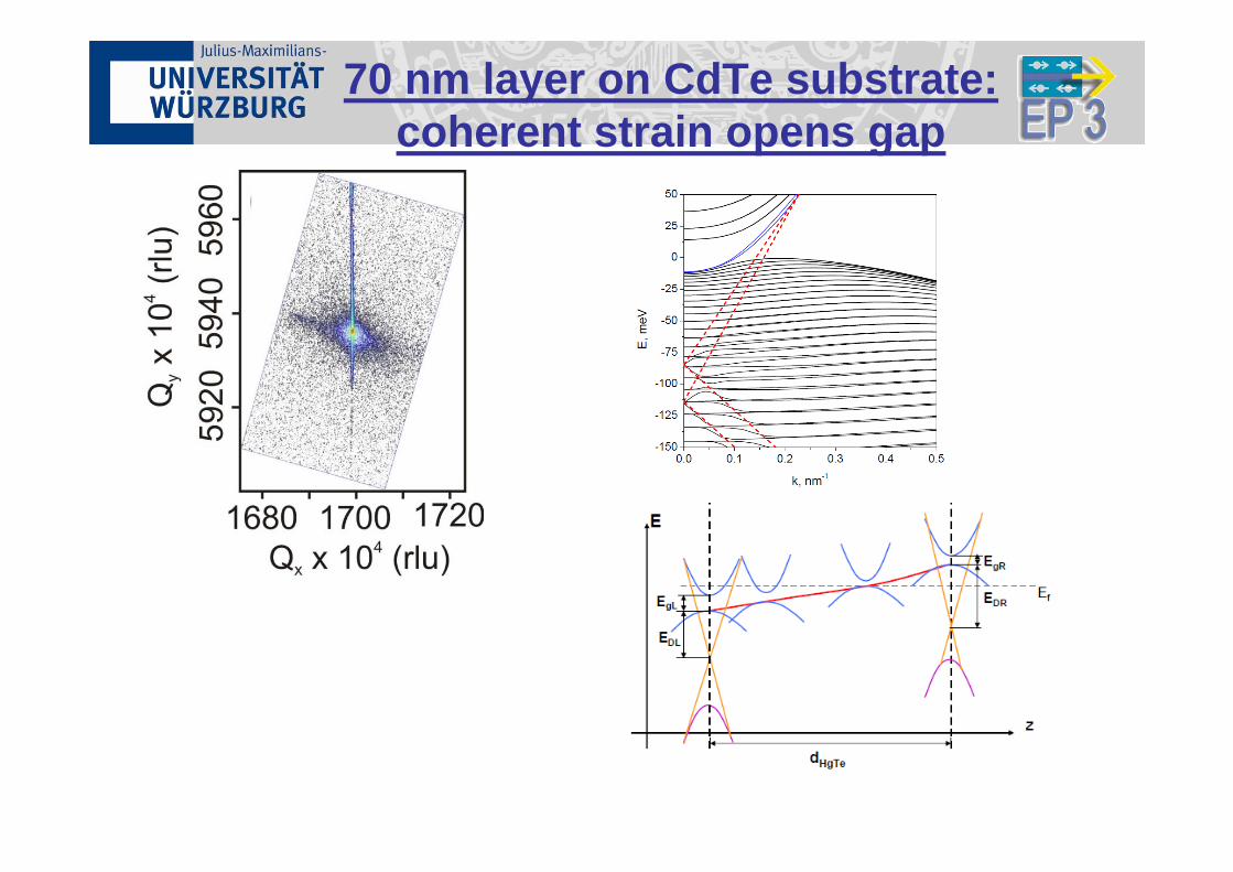
70 nm layer on CdTe substrate:coherent strain opens gap
0 2 4 6 8 10 12 14 160
2000
4000
6000
8000
10000
12000
14000
16000
0
2000
4000
6000
8000
10000
12000
14000
Rxx (SdH)
R
xx in
Ohm
B in Tesla
Rxy (Hall)
Rxy
in O
hm
Bulk HgTe as a 3-D Topological ‚Insulator‘
@ 20 mK: bulk conductivity almost frozen out - Surface state mobility ca. 35000 cm2/Vs
C. Brüne et al., Phys. Rev. Lett. 106, 126803 (2011).

3D HgTe-calculations
2 4 6 8 10 12 14 160
2000
4000
6000
8000
10000
2.73.54.45.67.69.711 33.94.96.78.510.112
experiment
Rxx
in O
hm
B in Tesla
n=3.7*1011 cm-2
n=4.85*1011 cm-2
n=(4.85+3.7)*1011 cm-2
DO
S
Red and blue lines : DOS for each of the Dirac-cones with the corresponding fixed 2D-density,Green line: the sum of the blue and red lines
C. Brüne et al., Phys. Rev. Lett. 106, 126803 (2011).
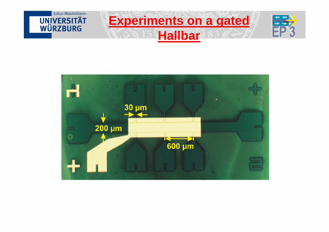
Experiments on a gatedHallbar
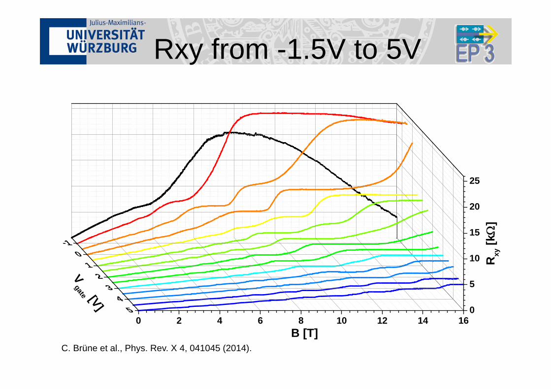
0 2 4 6 8 10 12 14 16
-10
12
34
5 0
5
10
15
20
25
Vgate [V]
B [T]
Rxy
[k
]
Rxy from -1.5V to 5V
C. Brüne et al., Phys. Rev. X 4, 041045 (2014).
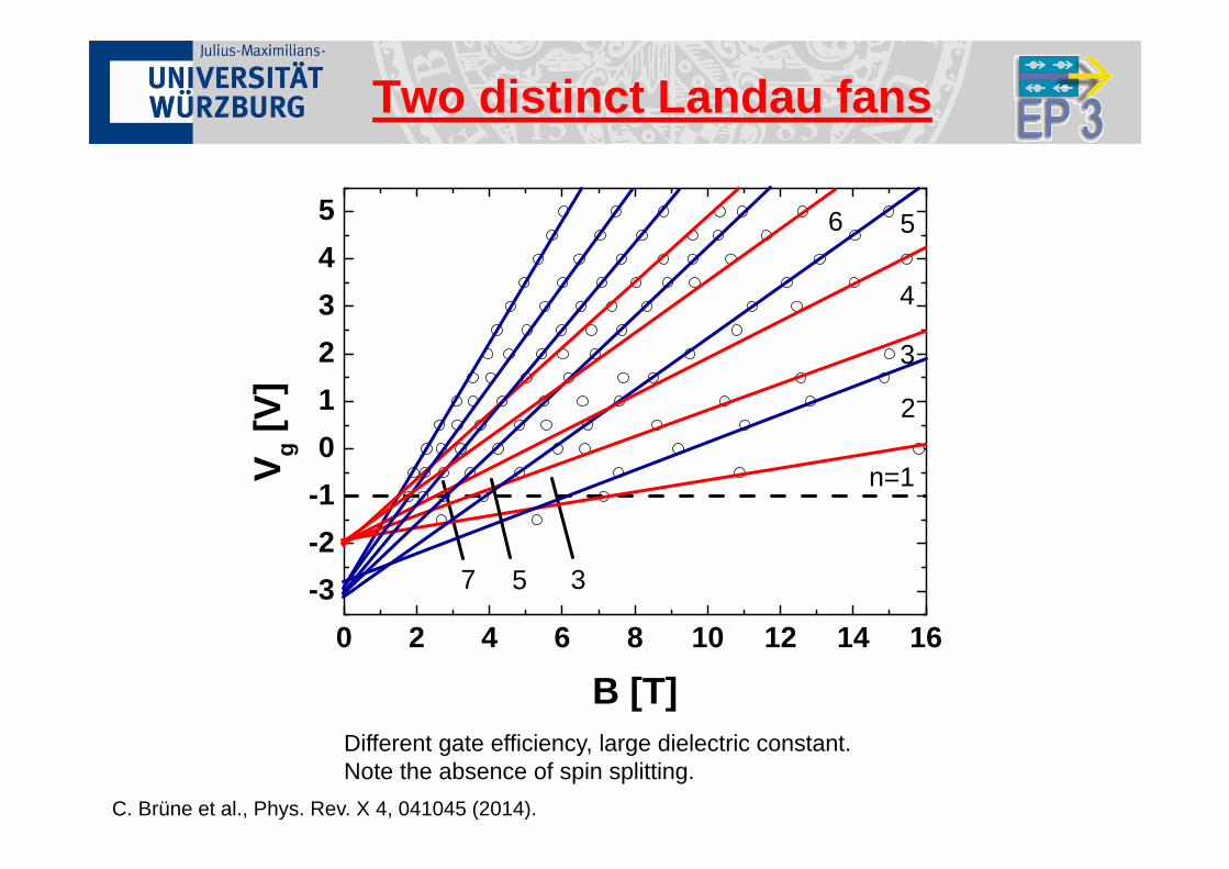
0 2 4 6 8 10 12 14 16-3-2-1012345
7 3
5
6
5
4
3
2
V g [V]
B [T]
n=1
Two distinct Landau fans
Different gate efficiency, large dielectric constant. Note the absence of spin splitting.
C. Brüne et al., Phys. Rev. X 4, 041045 (2014).
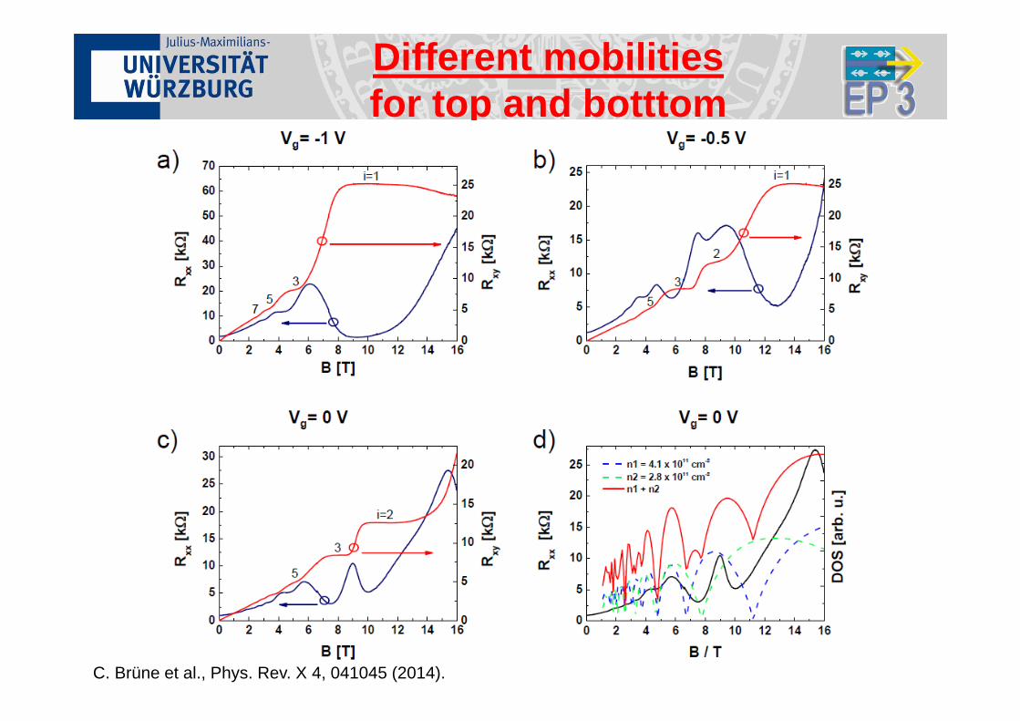
Different mobilitiesfor top and botttom
C. Brüne et al., Phys. Rev. X 4, 041045 (2014).

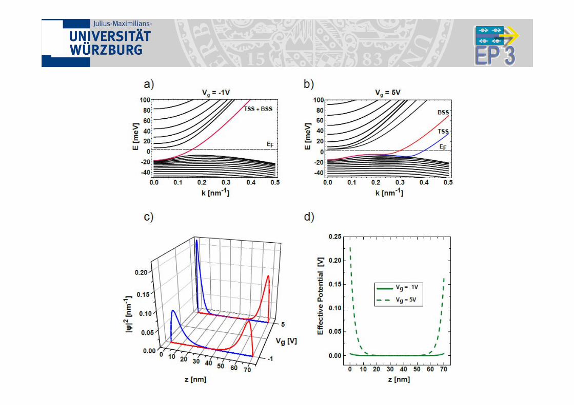
More plots
Constant (small) deviation Berry phase for Dirac fermions
Transport exclusively through surface states, for all gate voltages.Cause: Dirac systems have different screening properties from parabolic bands,resulting in a smaller dielectric constant(cf. E.H. Wang, S. das Sarma, Phys. Rev B 75, 205418 (2007), D. DiVincenzo, G. Mele, Phys. Rev B 29, 1685 (1984).
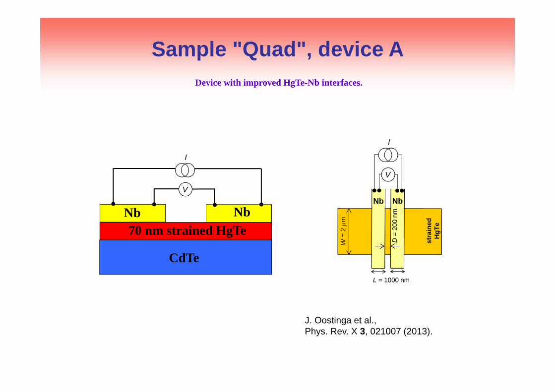
Sample "Quad", device ADevice with improved HgTe-Nb interfaces.
Nb Nb
CdTe
70 nm strained HgTe
I
V
W=
2 m
stra
ined
HgT
e
Nb Nb
L = 1000 nm
D=
200
nm
V
I
J. Oostinga et al., Phys. Rev. X 3, 021007 (2013).

Supercurrent regimeAt T = 25 mK, 200 mK, 500, 800 mK
-6 -4 -2 0 2 4 6
x 10-6
-2.5
-2
-1.5
-1
-0.5
0
0.5
1
1.5
2
2.5
x 10-4 I-V at different temperatures
I / A
Usa
mpl
e / V
800 mK500 mK200 mK
-1 -0.8 -0.6 -0.4 -0.2 0 0.2 0.4 0.6 0.8 1
x 10-5
-5
-4
-3
-2
-1
0
1
2
3
4
5x 10⁻⁴ I - V at B = 0 mT, T = 25 mK
I / A
Usa
mpl
e / V
20120411_004 (<-)20120412_001 (<-)20120412_002 (->)
sI
sIrI
rI
Switching current depends on sweeping direction (origin unknown):
Retrapping current does not depend on sweeping direction:
ss II rr II
IcRN 0.15-0.2 mV
At T = 25 mK:Ic Is 3-4 A
RN 50
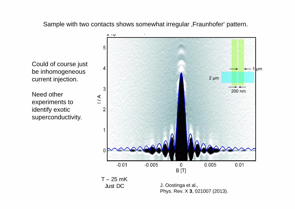
T 25 mKJust DC
Could of course just be inhomogeneouscurrent injection.
Need otherexperiments toidentify exoticsuperconductivity.
J. Oostinga et al., Phys. Rev. X 3, 021007 (2013).
Sample with two contacts shows somewhat irregular ‚Fraunhofer‘ pattern.
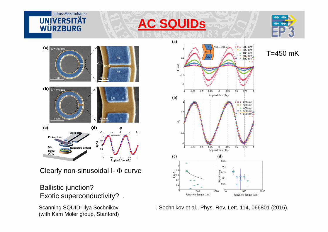
AC SQUIDs
Scanning SQUID: Ilya Sochnikov(with Kam Moler group, Stanford)
0 500 10000
0.2
0.4
0.6
0.8
1
0 500 10000
0.05
0.1
0.15
0.2
0.25
-1 -0.75 -0.5 -0.25 0 0.25 0.5 0.75 1
-1
-0.5
0
0.5
1
I (μA
)
Applied flux (Φ0)
Applied flux (Φ0)
I/Ic
(a)
(b)
L = 200 – 600 nm
Nb
HgTe
Asy
mm
etry
Junctions length (μm)Junctions length (μm)
I c(μ
A)
(c) (d)
200 nm300 nm400 nm500 nm600 nm
-1 -0.75 -0.5 -0.25 0 0.25 0.5 0.75 1
-1
-0.5
0
0.5
1
200 nm300 nm400 nm500 nm600 nm
Clearly non-sinusoidal I- curve
Ballistic junction?Exotic superconductivity? .
T=450 mK
I. Sochnikov et al., Phys. Rev. Lett. 114, 066801 (2015).
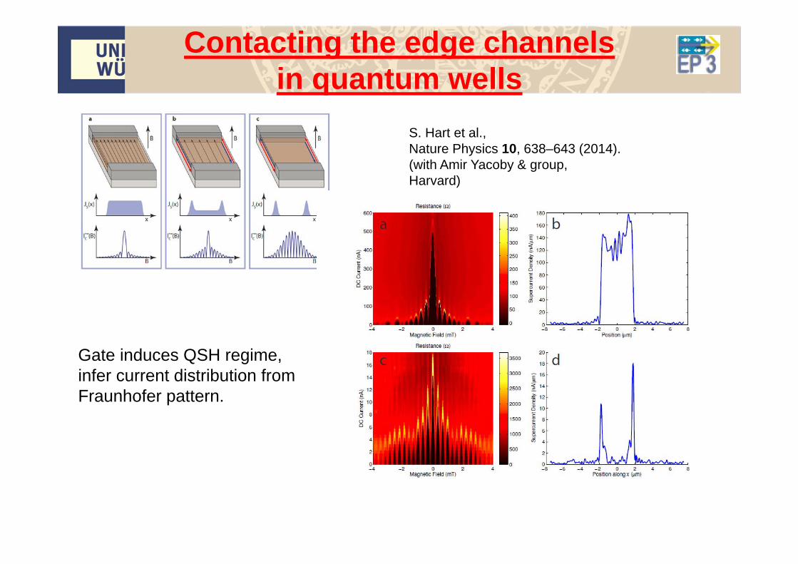
Contacting the edge channelsin quantum wells
S. Hart et al., Nature Physics 10, 638–643 (2014).(with Amir Yacoby & group, Harvard)
Gate induces QSH regime,infer current distribution fromFraunhofer pattern.
Conclusions– HgTe quantum wells: normal and inverted gap, linear (Dirac) dispersion
– show Quantum Spin Hall Effect
– demonstrated helical edge channels and spin polarization
– strained 3D layers show QHE of topological surface states
– In which a - very peculiar - supercurrent can be induced
Collaborators:Erwann Bocquillon, Christoph Brüne, Hartmut Buhmann, Markus König, Luis Maier, Matthias Mühlbauer, Jeroen Oostinga, Cornelius Thienel….Teun Klapwijk, David Goldhaber-Gordon, Kam Moler, Amir Yacoby, Andrei Pimenov, Marek Potemski, Seigo TaruchaTheory: Alena Novik, Ewelina Hankiewicz , Grigory Tkachov, BjörnTrauzettel (all @ Würzburg), Jairo Sinova (Mainz), Shoucheng Zhang, Xiaoliang Qi (Stanford), Chaoxing Liu (Penn State)
Funding: DFG (SPP Topological Insulators, DFG-JST FG Topotronics, Leibniz project), Humboldt Stiftung, EU-ERC AG “3-TOP”, DARPA