Embed Size (px)
Citation preview
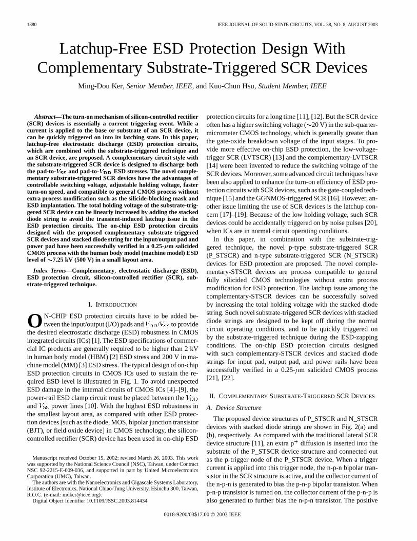
1380 IEEE JOURNAL OF SOLID-STATE CIRCUITS, VOL. 38, NO. 8, AUGUST 2003
Latchup-Free ESD Protection Design WithComplementary Substrate-Triggered SCR Devices
Ming-Dou Ker, Senior Member, IEEE,and Kuo-Chun Hsu, Student Member, IEEE
Abstract—The turn-on mechanism of silicon-controlled rectifier(SCR) devices is essentially a current triggering event. While acurrent is applied to the base or substrate of an SCR device, itcan be quickly triggered on into its latching state. In this paper,latchup-free electrostatic discharge (ESD) protection circuits,which are combined with the substrate-triggered technique andan SCR device, are proposed. A complementary circuit style withthe substrate-triggered SCR device is designed to discharge boththe pad-to- SS and pad-to- DD ESD stresses. The novel comple-mentary substrate-triggered SCR devices have the advantages ofcontrollable switching voltage, adjustable holding voltage, fasterturn-on speed, and compatible to general CMOS process withoutextra process modification such as the silicide-blocking mask andESD implantation. The total holding voltage of the substrate-trig-gered SCR device can be linearly increased by adding the stackeddiode string to avoid the transient-induced latchup issue in theESD protection circuits. The on-chip ESD protection circuitsdesigned with the proposed complementary substrate-triggeredSCR devices and stacked diode string for the input/output pad andpower pad have been successfully verified in a 0.25-m salicidedCMOS process with the human body model (machine model) ESDlevel of 7.25 kV (500 V) in a small layout area.
Index Terms—Complementary, electrostatic discharge (ESD),ESD protection circuit, silicon-controlled rectifier (SCR), sub-strate-triggered technique.
I. INTRODUCTION
ON-CHIP ESD protection circuits have to be added be-tween the input/output (I/O) pads and / to provide
the desired electrostatic discharge (ESD) robustness in CMOSintegrated circuits (ICs) [1]. The ESD specifications of commer-cial IC products are generally required to be higher than 2 kVin human body model (HBM) [2] ESD stress and 200 V in ma-chine model (MM) [3] ESD stress. The typical design of on-chipESD protection circuits in CMOS ICs used to sustain the re-quired ESD level is illustrated in Fig. 1. To avoid unexpectedESD damage in the internal circuits of CMOS ICs [4]–[9], thepower-rail ESD clamp circuit must be placed between theand power lines [10]. With the highest ESD robustness inthe smallest layout area, as compared with other ESD protec-tion devices [such as the diode, MOS, bipolar junction transistor(BJT), or field oxide device] in CMOS technology, the silicon-controlled rectifier (SCR) device has been used in on-chip ESD
Manuscript received October 15, 2002; revised March 26, 2003. This workwas supported by the National Science Council (NSC), Taiwan, under ContractNSC 92-2215-E-009-036, and supported in part by United MicroelectronicsCorporation (UMC), Taiwan.
The authors are with the Nanoelectronics and Gigascale Systems Laboratory,Institute of Electronics, National Chiao-Tung University, Hsinchu 300, Taiwan,R.O.C. (e-mail: [email protected]).
Digital Object Identifier 10.1109/JSSC.2003.814434
protection circuits for a long time [11], [12]. But the SCR deviceoften has a higher switching voltage (20 V) in the sub-quarter-micrometer CMOS technology, which is generally greater thanthe gate-oxide breakdown voltage of the input stages. To pro-vide more effective on-chip ESD protection, the low-voltage-trigger SCR (LVTSCR) [13] and the complementary-LVTSCR[14] were been invented to reduce the switching voltage of theSCR devices. Moreover, some advanced circuit techniques havebeen also applied to enhance the turn-on efficiency of ESD pro-tection circuits with SCR devices, such as the gate-coupled tech-nique [15] and the GGNMOS-triggered SCR [16]. However, an-other issue limiting the use of SCR devices is the latchup con-cern [17]–[19]. Because of the low holding voltage, such SCRdevices could be accidentally triggered on by noise pulses [20],when ICs are in normal circuit operating conditions.
In this paper, in combination with the substrate-trig-gered technique, the novel p-type substrate-triggered SCR(P_STSCR) and n-type substrate-triggered SCR (N_STSCR)devices for ESD protection are proposed. The novel comple-mentary-STSCR devices are process compatible to generalfully silicided CMOS technologies without extra processmodification for ESD protection. The latchup issue among thecomplementary-STSCR devices can be successfully solvedby increasing the total holding voltage with the stacked diodestring. Such novel substrate-triggered SCR devices with stackeddiode strings are designed to be kept off during the normalcircuit operating conditions, and to be quickly triggered onby the substrate-triggered technique during the ESD-zappingconditions. The on-chip ESD protection circuits designedwith such complementary-STSCR devices and stacked diodestrings for input pad, output pad, and power rails have beensuccessfully verified in a 0.25-m salicided CMOS process[21], [22].
II. COMPLEMENTARY SUBSTRATE-TRIGGEREDSCR DEVICES
A. Device Structure
The proposed device structures of P_STSCR and N_STSCRdevices with stacked diode strings are shown in Fig. 2(a) and(b), respectively. As compared with the traditional lateral SCRdevice structure [11], an extra pdiffusion is inserted into thesubstrate of the P_STSCR device structure and connected outas the p-trigger node of the P_STSCR device. When a triggercurrent is applied into this trigger node, the n-p-n bipolar tran-sistor in the SCR structure is active, and the collector current ofthe n-p-n is generated to bias the p-n-p bipolar transistor. Whenp-n-p transistor is turned on, the collector current of the p-n-p isalso generated to further bias the n-p-n transistor. The positive
0018-9200/03$17.00 © 2003 IEEE
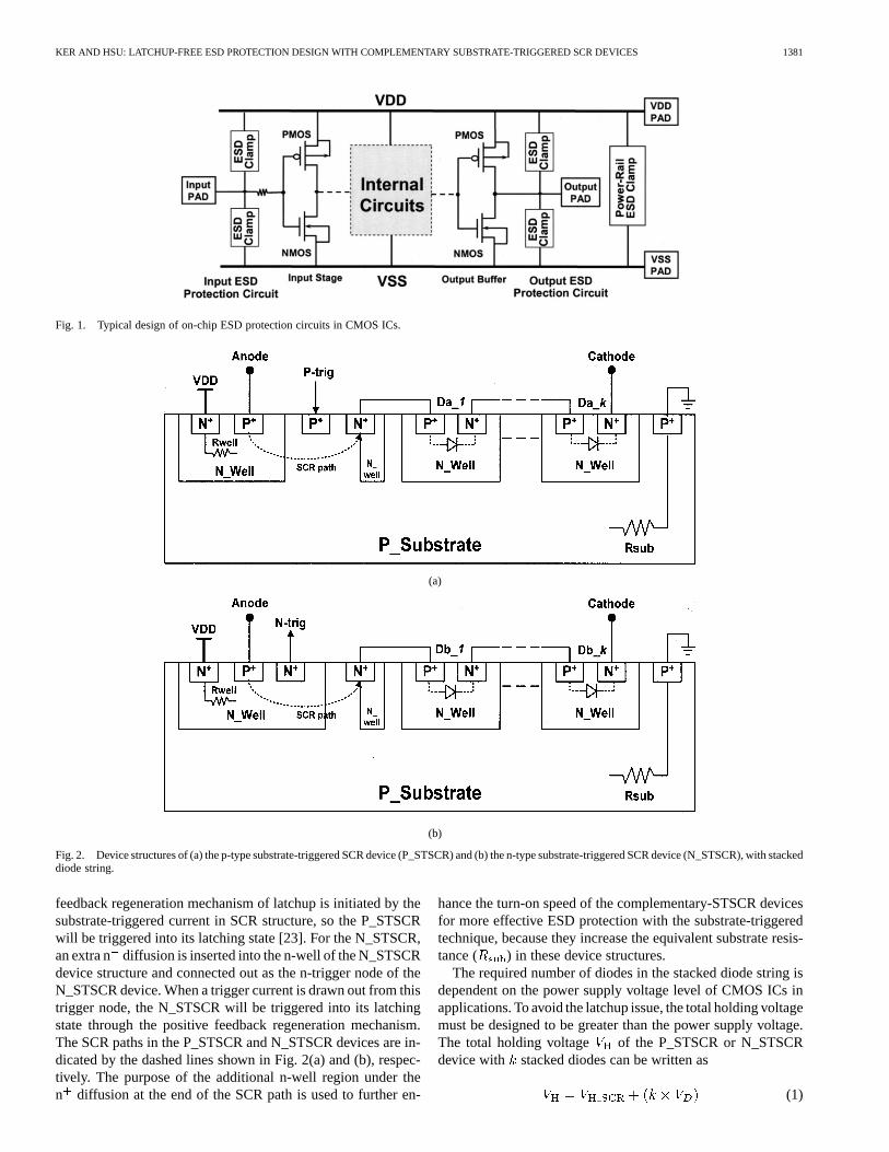
KER AND HSU: LATCHUP-FREE ESD PROTECTION DESIGN WITH COMPLEMENTARY SUBSTRATE-TRIGGERED SCR DEVICES 1381
Fig. 1. Typical design of on-chip ESD protection circuits in CMOS ICs.
(a)
(b)
Fig. 2. Device structures of (a) the p-type substrate-triggered SCR device (P_STSCR) and (b) the n-type substrate-triggered SCR device (N_STSCR), with stackeddiode string.
feedback regeneration mechanism of latchup is initiated by thesubstrate-triggered current in SCR structure, so the P_STSCRwill be triggered into its latching state [23]. For the N_STSCR,an extra n diffusion is inserted into the n-well of the N_STSCRdevice structure and connected out as the n-trigger node of theN_STSCR device. When a trigger current is drawn out from thistrigger node, the N_STSCR will be triggered into its latchingstate through the positive feedback regeneration mechanism.The SCR paths in the P_STSCR and N_STSCR devices are in-dicated by the dashed lines shown in Fig. 2(a) and (b), respec-tively. The purpose of the additional n-well region under then diffusion at the end of the SCR path is used to further en-
hance the turn-on speed of the complementary-STSCR devicesfor more effective ESD protection with the substrate-triggeredtechnique, because they increase the equivalent substrate resis-tance ( ) in these device structures.
The required number of diodes in the stacked diode string isdependent on the power supply voltage level of CMOS ICs inapplications. To avoid the latchup issue, the total holding voltagemust be designed to be greater than the power supply voltage.The total holding voltage of the P_STSCR or N_STSCRdevice with stacked diodes can be written as
(1)
1382 IEEE JOURNAL OF SOLID-STATE CIRCUITS, VOL. 38, NO. 8, AUGUST 2003
(a)
(b)
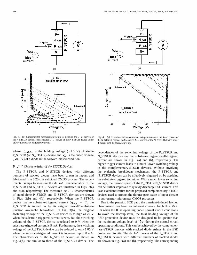
Fig. 3. (a) Experimental measurement setup to measure theI–V curves ofthe P_STSCR device. (b) MeasuredI–V curves of the P_STSCR device underdifferent substrate-triggered currents.
where is the holding voltage (1.5 V) of singleP_STSCR (or N_STSCR) device and is the cut-in voltage( 0.6 V) of a diode in the forward-biased condition.
B. – Characteristics of the STSCR Devices
The P_STSCR and N_STSCR devices with differentnumbers of stacked diodes have been drawn in layout andfabricated in a 0.25-m salicided CMOS process. The exper-imental setups to measure the dc– characteristics of theP_STSCR and N_STSCR devices are illustrated in Figs. 3(a)and 4(a), respectively. The measured dc– characteristicsof stand-alone P_STSCR and N_STSCR devices are shownin Figs. 3(b) and 4(b), respectively. When the P_STSCRdevice has no substrate-triggered current ( ), theP_STSCR is turned on by its original n-well/p-substratejunction avalanche breakdown. In Fig. 3(b), the originalswitching voltage of the P_STSCR device is as high as 22 Vwhen the substrate-triggered current is zero. But the switchingvoltage of the P_STSCR device is reduced to 9 V when thesubstrate-triggered current is 5 mA. Furthermore, the switchingvoltage of the P_STSCR device can be reduced to only 1.85 Vwhen the substrate-triggered current is increased up to 8 mA.The characteristics of the N_STSCR device, as shown inFig. 4(b), are similar to those of the P_STSCR device. The
(a)
(b)
Fig. 4. (a) Experimental measurement setup to measure theI–V curves ofthe N_STSCR device. (b) MeasuredI–V curves of the N_STSCR device underdifferent well-triggered currents.
dependences of the switching voltage of the P_STSCR andN_STSCR devices on the substrate-triggered/well-triggeredcurrent are shown in Fig. 5(a) and (b), respectively. Thehigher trigger current leads to a much lower switching voltagein the complementary-STSCR devices. Without involvingthe avalanche breakdown mechanism, the P_STSCR andN_STSCR devices can be effectively triggered on by applyingthe substrate-triggered technique. With a much lower switchingvoltage, the turn-on speed of the P_STSCR/N_STSCR devicecan be further improved to quickly discharge ESD current. Thisis an excellent feature for the proposed complementary-STSCRdevices used to protect the thinner gate oxide of input circuitsin sub-quarter-micrometer CMOS processes.
Due to the parasitic SCR path, the transient-induced latchupphenomenon has been an inherent concern for bulk CMOSICs when the IC is operating under normal circuit conditions.To avoid the latchup issue, the total holding voltage of theESD protection device must be designed to be greater thanthe maximum voltage level of during the normal circuitoperating conditions. This can be achieved by the complemen-tary-STSCR devices with stacked diode strings in the ESDprotection circuits. The dc– curves of the P_STSCR andN_STSCR devices with different numbers of stacked diodesare shown in Fig. 6(a) and (b), respectively. The corresponding

KER AND HSU: LATCHUP-FREE ESD PROTECTION DESIGN WITH COMPLEMENTARY SUBSTRATE-TRIGGERED SCR DEVICES 1383
(a)
(b)
Fig. 5. Dependence of the switching voltage of (a) the P_STSCR and (b) theN_STSCR on the triggered current in p-substrate or in n-well.
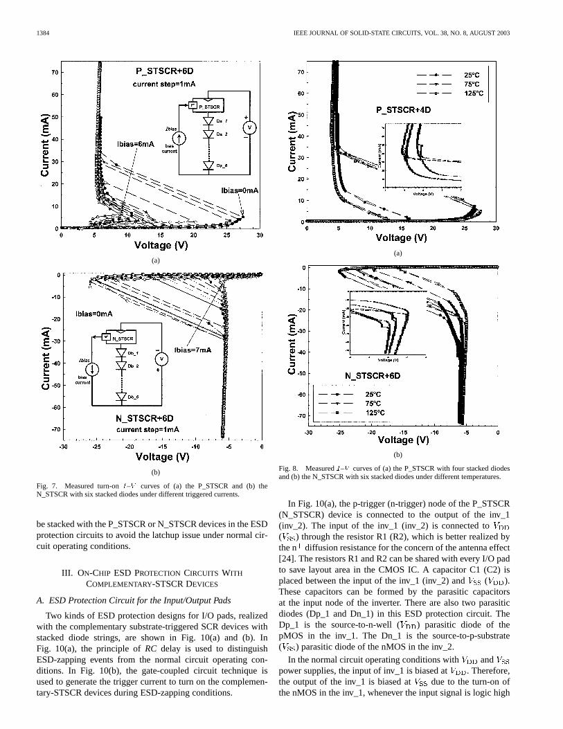
measurement setups are inset into Fig. 6(a) and (b), respec-tively. The total holding voltages of the complementary-STSCRdevices with stacked diode strings can be raised by increasingthe number of stacked diodes. The holding voltages of thecomplementary-STSCR devices with one, two, four, and sixdiodes at the temperature of 25C are 2.6, 3.2, 4.6, and 5.8 V,respectively. The switching voltages of complementary-STSCRdevices with stacked diode strings shown in Fig. 6 have a littleincrease when increasing the number of stacked diodes, butthey can be reduced by the substrate-triggered technique toprovide effective ESD protection. Fig. 7(a) and (b) shows the– curves of the P_STSCR and N_STSCR with six diodes
under different substrate- or well-triggered currents, respec-tively. With the substrate-triggered technique, the switchingvoltages of the P_STSCR and N_STSCR with six diodes can besignificantly reduced. Thus, the proposed P_STSCR/N_STSCRwith stacked diode strings have the adjustable holding voltageand controllable switching voltage, so they can provide effec-tive ESD protection for internal circuits as well as avoid thetransient-induced latchup issue.
For precise design of the ESD protection circuits, the devicecharacteristics of complementary-STSCR devices must be
(a)
(b)
Fig. 6. MeasuredI–V curves of (a) the P_STSCR and (b) the N_STSCR withdifferent numbers of stacked diodes under 25C temperature.
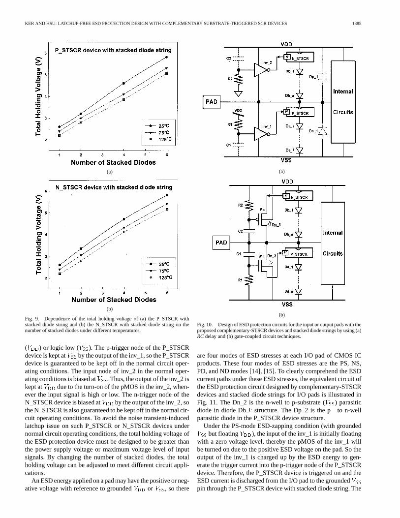
calibrated under different temperatures. The dc– curves ofa P_STSCR with four diodes and an N_STSCR with six diodesunder different temperatures are measured in Fig. 8(a) and (b),respectively. The insets in Fig. 8(a) and (b) are the enlargedviews around the holding point for clear observation. Theholding voltages of the P_STSCR with four diodes at the tem-peratures of 25C, 75 C, and 125 C are 4.6, 4.1, and 3.85 V,respectively. The dependences of the total holding voltage ofthe P_STSCR and N_STSCR with stacked diode strings onthe number of stacked diodes under different temperatures areshown in Fig. 9(a) and (b), respectively. With increase of thenumber of stacked diodes, the holding voltages of such ESDprotection devices are increased. The total holding voltagesslightly reduce when the temperature is increased, because thecurrent gain of the parasitic bipolar transistor in the SCRdevice is enhanced with the increase of temperature. For safeapplications in 2.5-V CMOS ICs, two diodes are suggested to
1384 IEEE JOURNAL OF SOLID-STATE CIRCUITS, VOL. 38, NO. 8, AUGUST 2003
(a)
(b)
Fig. 7. Measured turn-onI–V curves of (a) the P_STSCR and (b) theN_STSCR with six stacked diodes under different triggered currents.
be stacked with the P_STSCR or N_STSCR devices in the ESDprotection circuits to avoid the latchup issue under normal cir-cuit operating conditions.
III. ON-CHIP ESD PROTECTION CIRCUITS WITH
COMPLEMENTARY-STSCR DEVICES
A. ESD Protection Circuit for the Input/Output Pads
Two kinds of ESD protection designs for I/O pads, realizedwith the complementary substrate-triggered SCR devices withstacked diode strings, are shown in Fig. 10(a) and (b). InFig. 10(a), the principle ofRC delay is used to distinguishESD-zapping events from the normal circuit operating con-ditions. In Fig. 10(b), the gate-coupled circuit technique isused to generate the trigger current to turn on the complemen-tary-STSCR devices during ESD-zapping conditions.
(a)
(b)
Fig. 8. MeasuredI–V curves of (a) the P_STSCR with four stacked diodesand (b) the N_STSCR with six stacked diodes under different temperatures.
In Fig. 10(a), the p-trigger (n-trigger) node of the P_STSCR(N_STSCR) device is connected to the output of the inv_1(inv_2). The input of the inv_1 (inv_2) is connected to( ) through the resistor R1 (R2), which is better realized bythe n diffusion resistance for the concern of the antenna effect[24]. The resistors R1 and R2 can be shared with every I/O padto save layout area in the CMOS IC. A capacitor C1 (C2) isplaced between the input of the inv_1 (inv_2) and ( ).These capacitors can be formed by the parasitic capacitorsat the input node of the inverter. There are also two parasiticdiodes (Dp_1 and Dn_1) in this ESD protection circuit. TheDp_1 is the source-to-n-well ( ) parasitic diode of thepMOS in the inv_1. The Dn_1 is the source-to-p-substrate( ) parasitic diode of the nMOS in the inv_2.
In the normal circuit operating conditions with andpower supplies, the input of inv_1 is biased at . Therefore,the output of the inv_1 is biased at due to the turn-on ofthe nMOS in the inv_1, whenever the input signal is logic high
KER AND HSU: LATCHUP-FREE ESD PROTECTION DESIGN WITH COMPLEMENTARY SUBSTRATE-TRIGGERED SCR DEVICES 1385
(a)
(b)
Fig. 9. Dependence of the total holding voltage of (a) the P_STSCR withstacked diode string and (b) the N_STSCR with stacked diode string on thenumber of stacked diodes under different temperatures.
( ) or logic low ( ). The p-trigger node of the P_STSCRdevice is kept at by the output of the inv_1, so the P_STSCRdevice is guaranteed to be kept off in the normal circuit oper-ating conditions. The input node of inv_2 in the normal oper-ating conditions is biased at . Thus, the output of the inv_2 iskept at due to the turn-on of the pMOS in the inv_2, when-ever the input signal is high or low. The n-trigger node of theN_STSCR device is biased at by the output of the inv_2, sothe N_STSCR is also guaranteed to be kept off in the normal cir-cuit operating conditions. To avoid the noise transient-inducedlatchup issue on such P_STSCR or N_STSCR devices undernormal circuit operating conditions, the total holding voltage ofthe ESD protection device must be designed to be greater thanthe power supply voltage or maximum voltage level of inputsignals. By changing the number of stacked diodes, the totalholding voltage can be adjusted to meet different circuit appli-cations.
An ESD energy applied on a pad may have the positive or neg-ative voltage with reference to grounded or , so there
(a)
(b)
Fig. 10. Design of ESD protection circuits for the input or output pads with theproposed complementary-STSCR devices and stacked diode strings by using (a)RCdelay and (b) gate-coupled circuit techniques.
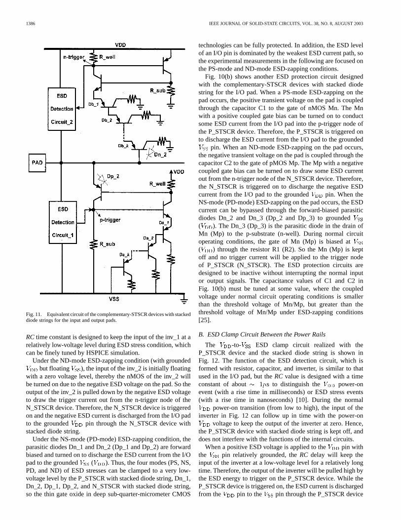
are four modes of ESD stresses at each I/O pad of CMOS ICproducts. These four modes of ESD stresses are the PS, NS,PD, and ND modes [14], [15]. To clearly comprehend the ESDcurrent paths under these ESD stresses, the equivalent circuit ofthe ESD protection circuit designed by complementary-STSCRdevices and stacked diode strings for I/O pads is illustrated inFig. 11. The Dn_2 is the n-well to p-substrate () parasiticdiode in diode Db structure. The Dp_2 is the pto n-wellparasitic diode in the P_STSCR device structure.
Under the PS-mode ESD-zapping condition (with groundedbut floating ), the input of the inv_1 is initially floating
with a zero voltage level, thereby the pMOS of the inv_1 willbe turned on due to the positive ESD voltage on the pad. So theoutput of the inv_1 is charged up by the ESD energy to gen-erate the trigger current into the p-trigger node of the P_STSCRdevice. Therefore, the P_STSCR device is triggered on and theESD current is discharged from the I/O pad to the groundedpin through the P_STSCR device with stacked diode string. The
1386 IEEE JOURNAL OF SOLID-STATE CIRCUITS, VOL. 38, NO. 8, AUGUST 2003
Fig. 11. Equivalent circuit of the complementary-STSCR devices with stackeddiode strings for the input and output pads.
RCtime constant is designed to keep the input of the inv_1 at arelatively low-voltage level during ESD stress condition, whichcan be finely tuned by HSPICE simulation.
Under the ND-mode ESD-zapping condition (with groundedbut floating ), the input of the inv_2 is initially floating
with a zero voltage level, thereby the nMOS of the inv_2 willbe turned on due to the negative ESD voltage on the pad. So theoutput of the inv_2 is pulled down by the negative ESD voltageto draw the trigger current out from the n-trigger node of theN_STSCR device. Therefore, the N_STSCR device is triggeredon and the negative ESD current is discharged from the I/O padto the grounded pin through the N_STSCR device withstacked diode string.
Under the NS-mode (PD-mode) ESD-zapping condition, theparasitic diodes Dn_1 and Dn_2 (Dp_1 and Dp_2) are forwardbiased and turned on to discharge the ESD current from the I/Opad to the grounded ( ). Thus, the four modes (PS, NS,PD, and ND) of ESD stresses can be clamped to a very low-voltage level by the P_STSCR with stacked diode string, Dn_1,Dn_2, Dp_1, Dp_2, and N_STSCR with stacked diode string,so the thin gate oxide in deep sub-quarter-micrometer CMOS
technologies can be fully protected. In addition, the ESD levelof an I/O pin is dominated by the weakest ESD current path, sothe experimental measurements in the following are focused onthe PS-mode and ND-mode ESD-zapping conditions.
Fig. 10(b) shows another ESD protection circuit designedwith the complementary-STSCR devices with stacked diodestring for the I/O pad. When a PS-mode ESD-zapping on thepad occurs, the positive transient voltage on the pad is coupledthrough the capacitor C1 to the gate of nMOS Mn. The Mnwith a positive coupled gate bias can be turned on to conductsome ESD current from the I/O pad into the p-trigger node ofthe P_STSCR device. Therefore, the P_STSCR is triggered onto discharge the ESD current from the I/O pad to the grounded
pin. When an ND-mode ESD-zapping on the pad occurs,the negative transient voltage on the pad is coupled through thecapacitor C2 to the gate of pMOS Mp. The Mp with a negativecoupled gate bias can be turned on to draw some ESD currentout from the n-trigger node of the N_STSCR device. Therefore,the N_STSCR is triggered on to discharge the negative ESDcurrent from the I/O pad to the grounded pin. When theNS-mode (PD-mode) ESD-zapping on the pad occurs, the ESDcurrent can be bypassed through the forward-biased parasiticdiodes Dn_2 and Dn_3 (Dp_2 and Dp_3) to grounded( ). The Dn_3 (Dp_3) is the parasitic diode in the drain ofMn (Mp) to the p-substrate (n-well). During normal circuitoperating conditions, the gate of Mn (Mp) is biased at( ) through the resistor R1 (R2). So the Mn (Mp) is keptoff and no trigger current will be applied to the trigger nodeof P_STSCR (N_STSCR). The ESD protection circuits aredesigned to be inactive without interrupting the normal inputor output signals. The capacitance values of C1 and C2 inFig. 10(b) must be tuned at some value, where the coupledvoltage under normal circuit operating conditions is smallerthan the threshold voltage of Mn/Mp, but greater than thethreshold voltage of Mn/Mp under ESD-zapping conditions[25].
B. ESD Clamp Circuit Between the Power Rails
The -to- ESD clamp circuit realized with theP_STSCR device and the stacked diode string is shown inFig. 12. The function of the ESD detection circuit, which isformed with resistor, capacitor, and inverter, is similar to thatused in the I/O pad, but theRC value is designed with a timeconstant of about 1 s to distinguish the power-onevent (with a rise time in milliseconds) or ESD stress events(with a rise time in nanoseconds) [10]. During the normal
power-on transition (from low to high), the input of theinverter in Fig. 12 can follow up in time with the power-on
voltage to keep the output of the inverter at zero. Hence,the P_STSCR device with stacked diode string is kept off, anddoes not interfere with the functions of the internal circuits.
When a positive ESD voltage is applied to the pin withthe pin relatively grounded, theRC delay will keep theinput of the inverter at a low-voltage level for a relatively longtime. Therefore, the output of the inverter will be pulled high bythe ESD energy to trigger on the P_STSCR device. While theP_STSCR device is triggered on, the ESD current is dischargedfrom the pin to the pin through the P_STSCR device
KER AND HSU: LATCHUP-FREE ESD PROTECTION DESIGN WITH COMPLEMENTARY SUBSTRATE-TRIGGERED SCR DEVICES 1387
Fig. 12. V -to-V ESD clamp circuit realized with P_STSCR and stackeddiode string.
and the stacked diode string. With such a suitable ESD detec-tion circuit, the P_STSCR device can be quickly triggered onto discharge the ESD current. When a negative ESD voltage isapplied to the pin with the pin relatively grounded, thenegative ESD current can be discharged from the pin to the
pin through the forward-biased P-substrate ()-to-n-well(which is connected to ) parasitic diode. In addition, byadjusting the number of stacked diodes, such power-rail ESDclamp circuits can be designed free of the latchup issue. Witha suitable ESD detection circuit, the N_STSCR device can bealso designed for the power-rail ESD clamp circuit.
IV. EXPERIMENTAL RESULTS
A. ESD Robustness
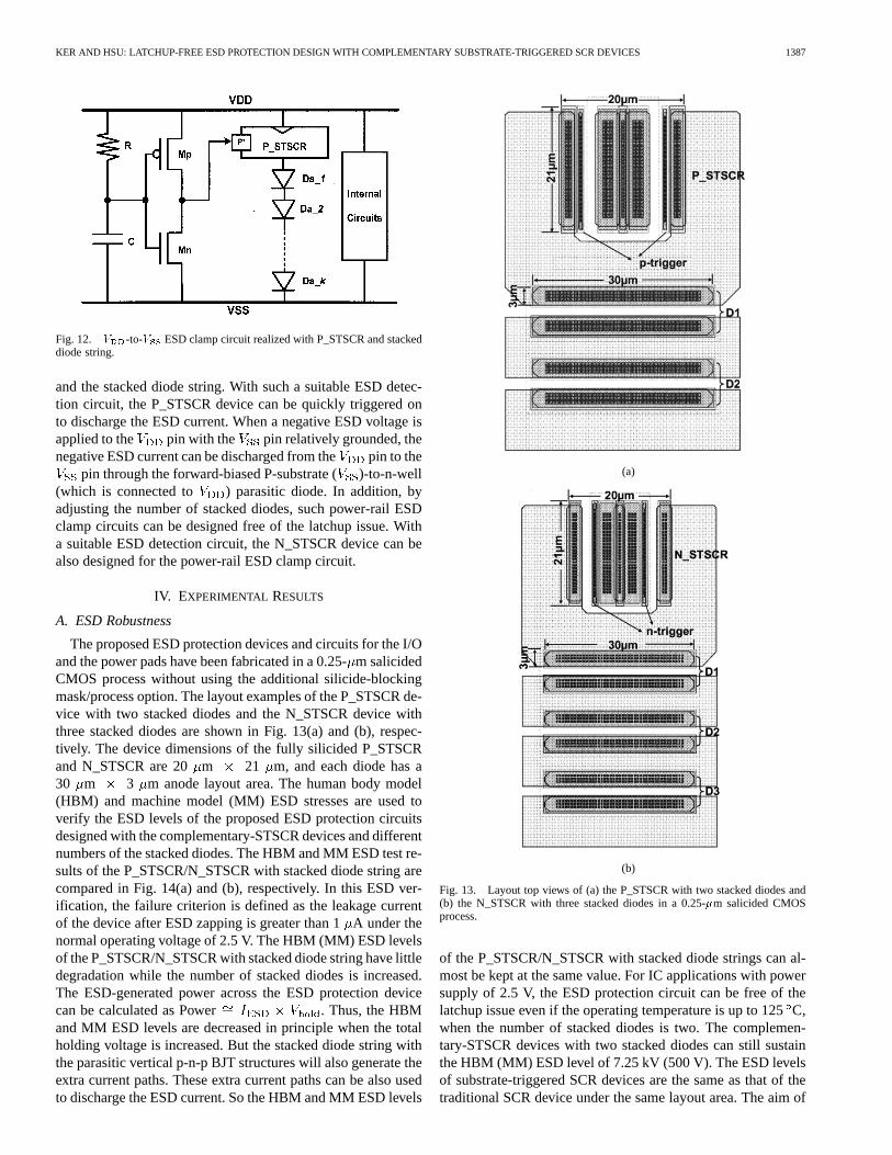
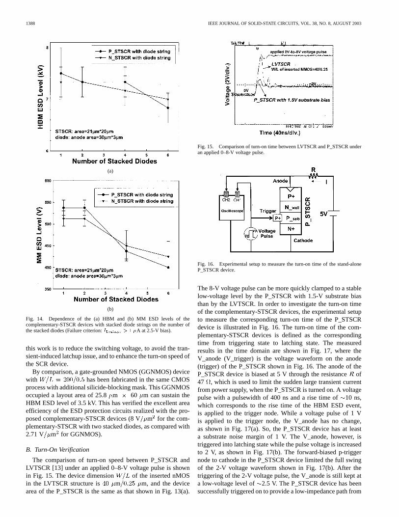
The proposed ESD protection devices and circuits for the I/Oand the power pads have been fabricated in a 0.25-m salicidedCMOS process without using the additional silicide-blockingmask/process option. The layout examples of the P_STSCR de-vice with two stacked diodes and the N_STSCR device withthree stacked diodes are shown in Fig. 13(a) and (b), respec-tively. The device dimensions of the fully silicided P_STSCRand N_STSCR are 20m 21 m, and each diode has a30 m 3 m anode layout area. The human body model(HBM) and machine model (MM) ESD stresses are used toverify the ESD levels of the proposed ESD protection circuitsdesigned with the complementary-STSCR devices and differentnumbers of the stacked diodes. The HBM and MM ESD test re-sults of the P_STSCR/N_STSCR with stacked diode string arecompared in Fig. 14(a) and (b), respectively. In this ESD ver-ification, the failure criterion is defined as the leakage currentof the device after ESD zapping is greater than 1A under thenormal operating voltage of 2.5 V. The HBM (MM) ESD levelsof the P_STSCR/N_STSCR with stacked diode string have littledegradation while the number of stacked diodes is increased.The ESD-generated power across the ESD protection devicecan be calculated as Power . Thus, the HBMand MM ESD levels are decreased in principle when the totalholding voltage is increased. But the stacked diode string withthe parasitic vertical p-n-p BJT structures will also generate theextra current paths. These extra current paths can be also usedto discharge the ESD current. So the HBM and MM ESD levels
(a)
(b)
Fig. 13. Layout top views of (a) the P_STSCR with two stacked diodes and(b) the N_STSCR with three stacked diodes in a 0.25-�m salicided CMOSprocess.
of the P_STSCR/N_STSCR with stacked diode strings can al-most be kept at the same value. For IC applications with powersupply of 2.5 V, the ESD protection circuit can be free of thelatchup issue even if the operating temperature is up to 125C,when the number of stacked diodes is two. The complemen-tary-STSCR devices with two stacked diodes can still sustainthe HBM (MM) ESD level of 7.25 kV (500 V). The ESD levelsof substrate-triggered SCR devices are the same as that of thetraditional SCR device under the same layout area. The aim of
1388 IEEE JOURNAL OF SOLID-STATE CIRCUITS, VOL. 38, NO. 8, AUGUST 2003
(a)
(b)
Fig. 14. Dependence of the (a) HBM and (b) MM ESD levels of thecomplementary-STSCR devices with stacked diode strings on the number ofthe stacked diodes (Failure criterion:I > 1 �A at 2.5-V bias).
this work is to reduce the switching voltage, to avoid the tran-sient-induced latchup issue, and to enhance the turn-on speed ofthe SCR device.
By comparison, a gate-grounded NMOS (GGNMOS) devicewith has been fabricated in the same CMOSprocess with additional silicide-blocking mask. This GGNMOSoccupied a layout area of 25.8m 60 m can sustain theHBM ESD level of 3.5 kV. This has verified the excellent areaefficiency of the ESD protection circuits realized with the pro-posed complementary-STSCR devices (8 Vm for the com-plementary-STSCR with two stacked diodes, as compared with2.71 V m for GGNMOS).
B. Turn-On Verification
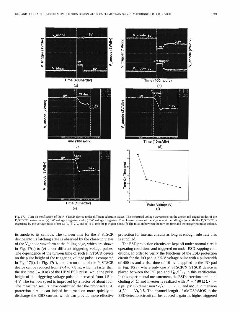
The comparison of turn-on speed between P_STSCR andLVTSCR [13] under an applied 0–8-V voltage pulse is shownin Fig. 15. The device dimension of the inserted nMOSin the LVTSCR structure is m m, and the devicearea of the P_STSCR is the same as that shown in Fig. 13(a).
Fig. 15. Comparison of turn-on time between LVTSCR and P_STSCR underan applied 0–8-V voltage pulse.
Fig. 16. Experimental setup to measure the turn-on time of the stand-aloneP_STSCR device.
The 8-V voltage pulse can be more quickly clamped to a stablelow-voltage level by the P_STSCR with 1.5-V substrate biasthan by the LVTSCR. In order to investigate the turn-on timeof the complementary-STSCR devices, the experimental setupto measure the corresponding turn-on time of the P_STSCRdevice is illustrated in Fig. 16. The turn-on time of the com-plementary-STSCR devices is defined as the correspondingtime from triggering state to latching state. The measuredresults in the time domain are shown in Fig. 17, where theV_anode (V_trigger) is the voltage waveform on the anode(trigger) of the P_STSCR shown in Fig. 16. The anode of theP_STSCR device is biased at 5 V through the resistanceof47 , which is used to limit the sudden large transient currentfrom power supply, when the P_STSCR is turned on. A voltagepulse with a pulsewidth of 400 ns and a rise time of10 ns,which corresponds to the rise time of the HBM ESD event,is applied to the trigger node. While a voltage pulse of 1 Vis applied to the trigger node, the V_anode has no change,as shown in Fig. 17(a). So, the P_STSCR device has at leasta substrate noise margin of 1 V. The V_anode, however, istriggered into latching state while the pulse voltage is increasedto 2 V, as shown in Fig. 17(b). The forward-biased p-triggernode to cathode in the P_STSCR device limited the full swingof the 2-V voltage waveform shown in Fig. 17(b). After thetriggering of the 2-V voltage pulse, the V_anode is still kept ata low-voltage level of 2.5 V. The P_STSCR device has beensuccessfully triggered on to provide a low-impedance path from
KER AND HSU: LATCHUP-FREE ESD PROTECTION DESIGN WITH COMPLEMENTARY SUBSTRATE-TRIGGERED SCR DEVICES 1389
Fig. 17. Turn-on verification of the P_STSCR device under different substrate biases. The measured voltage waveforms on the anode and trigger nodes of theP_STSCR device under (a) 1-V voltage triggering and (b) 2-V voltage triggering. The close-up views of the V_anode at the falling edge while the P_STSCRistriggering by the voltage pulse of (c) 1.5 V, (d) 2 V, and (e) 4 V, into the p-trigger node. (f) The relation between the turn-on time and the triggering pulse voltage.
its anode to its cathode. The turn-on time for the P_STSCRdevice into its latching state is observed by the close-up viewsof the V_anode waveform at the falling edge, which are shownin Fig. 17(c) to (e) under different triggering voltage pulses.The dependence of the turn-on time of such P_STSCR deviceon the pulse height of the triggering voltage pulse is comparedin Fig. 17(f). In Fig. 17(f), the turn-on time of the P_STSCRdevice can be reduced from 27.4 to 7.8 ns, which is faster thanthe rise time ( 10 ns) of the HBM ESD pulse, while the pulseheight of the triggering voltage pulse is increased from 1.5 to4 V. The turn-on speed is improved by a factor of about four.The measured results have confirmed that the proposed ESDprotection circuit can indeed be turned on more quickly todischarge the ESD current, which can provide more effective
protection for internal circuits as long as enough substrate biasis supplied.
The ESD protection circuits are kept off under normal circuitoperating conditions and triggered on under ESD-zapping con-ditions. In order to verify the functions of the ESD protectioncircuit for the I/O pad, a 2.5-V voltage pulse with a pulsewidthof 400 ns and a rise time of 10 ns is applied to the I/O padin Fig. 10(a), where only one P_STSCR/N_STSCR device isplaced between the I/O pad and / in this verification.In this experimental measurement, the ESD detection circuit in-cludingR, C, and inverter is realized with k ,
pF, pMOS dimension , and nMOS dimension. The channel length of nMOS/pMOS in the
ESD detection circuit can be reduced to gain the higher triggered
1390 IEEE JOURNAL OF SOLID-STATE CIRCUITS, VOL. 38, NO. 8, AUGUST 2003
(a) (b)
(c)
Fig. 18. Measured voltage waveforms on the I/O pad of Fig. 10(a) under (a) the normal circuit operating conditions, (b) the positive-to-V ESD-zapping conditionwhen a 2.5-V voltage pulse is applied to the I/O pad, and (c) the negative-to-V ESD-zapping condition when a�2.5-V voltage pulse is applied to the I/O pad.
currents. These device dimensions can be finetuned by HSPICEsimulator to fit different circuit applications. During the normalcircuit operating conditions, where the is power-on andis connected to ground, the input signal of 2.5 V has no degrada-tion, as shown in Fig. 18(a). So the ESD protection circuit doesnot interfere with the input signal. However, during the PS-modeESD-zapping condition, the ESD detection circuit is active, sothe applied voltage pulse of 2.5 V is clamped to1.2 V by theturned-on P_STSCR, as shown in Fig. 18(b). During ND-modeESD-zapping condition, a 2.5-V voltage pulse is clamped to
1.26 V by the turned-on N_STSCR, as shown in Fig. 18(c).By using this method, the turn-on characteristics of the ESDprotection circuit for the I/O pad shown in Fig. 10(b) can alsobe verified. In this measurement, the ESD detection circuit in-cluding C, R, and nMOS/pMOS is realized with fF,
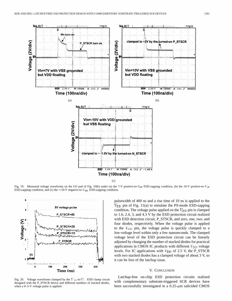
k , nMOS dimension , and pMOSdimension . When a positive 0–7-V voltagepulse to simulate the PS-mode ESD-zapping condition is ap-plied to the I/O pad of the ESD protection circuit in Fig. 10(b),the voltage waveform on the I/O pad is clamped to a low-voltagelevel measured in Fig. 19(a). In Fig. 19(a), the nMOS, Mn in theESD protection circuit of Fig. 10(b), will be first turned on toconduct some ESD current to trigger on the P_STSCR device,
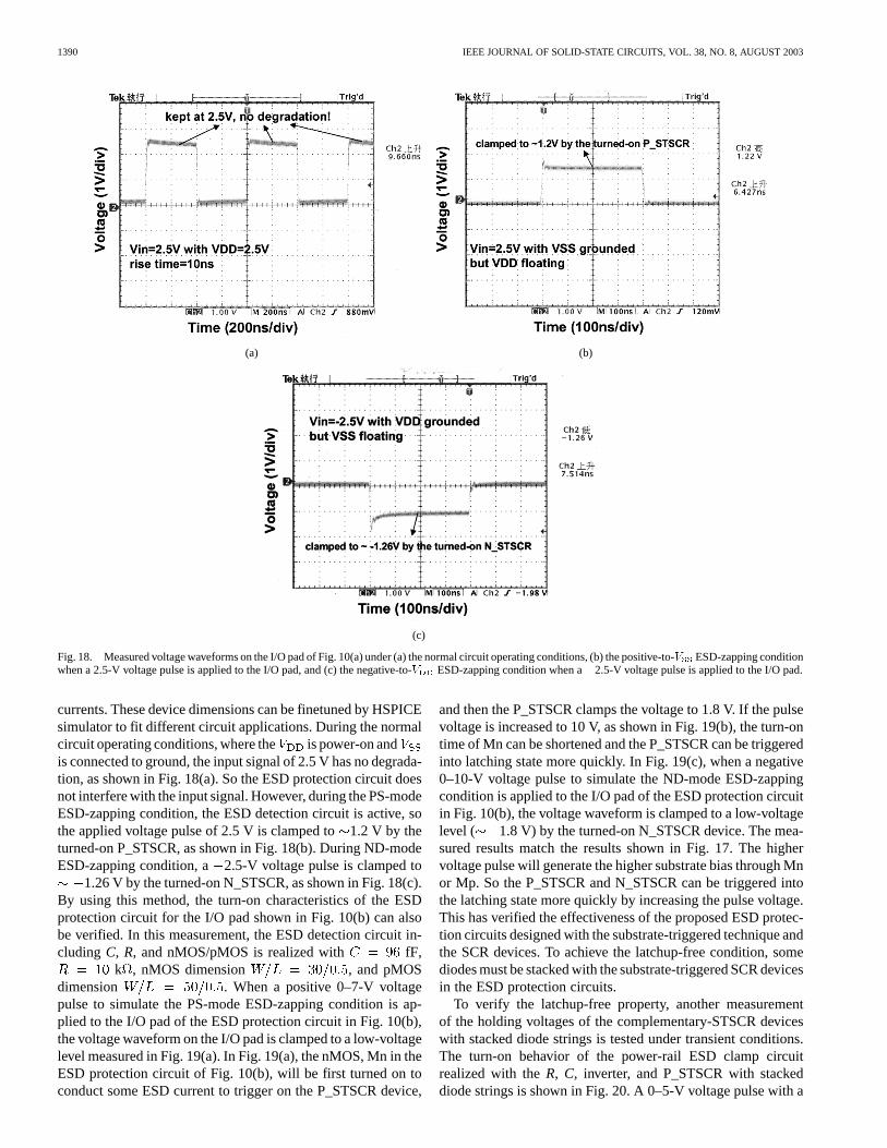
and then the P_STSCR clamps the voltage to 1.8 V. If the pulsevoltage is increased to 10 V, as shown in Fig. 19(b), the turn-ontime of Mn can be shortened and the P_STSCR can be triggeredinto latching state more quickly. In Fig. 19(c), when a negative0–10-V voltage pulse to simulate the ND-mode ESD-zappingcondition is applied to the I/O pad of the ESD protection circuitin Fig. 10(b), the voltage waveform is clamped to a low-voltagelevel ( 1.8 V) by the turned-on N_STSCR device. The mea-sured results match the results shown in Fig. 17. The highervoltage pulse will generate the higher substrate bias through Mnor Mp. So the P_STSCR and N_STSCR can be triggered intothe latching state more quickly by increasing the pulse voltage.This has verified the effectiveness of the proposed ESD protec-tion circuits designed with the substrate-triggered technique andthe SCR devices. To achieve the latchup-free condition, somediodes must be stacked with the substrate-triggered SCR devicesin the ESD protection circuits.
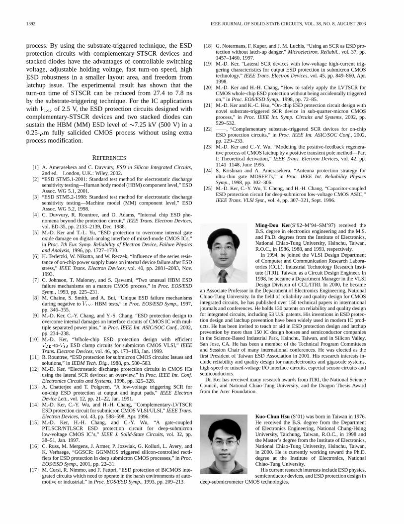
To verify the latchup-free property, another measurementof the holding voltages of the complementary-STSCR deviceswith stacked diode strings is tested under transient conditions.The turn-on behavior of the power-rail ESD clamp circuitrealized with theR, C, inverter, and P_STSCR with stackeddiode strings is shown in Fig. 20. A 0–5-V voltage pulse with a
KER AND HSU: LATCHUP-FREE ESD PROTECTION DESIGN WITH COMPLEMENTARY SUBSTRATE-TRIGGERED SCR DEVICES 1391
(a) (b)
(c)
Fig. 19. Measured voltage waveforms on the I/O pad of Fig. 10(b) under (a) the 7-V positive-to-V ESD-zapping condition, (b) the 10-V positive-to-V
ESD-zapping condition, and (c) the�10-V negative-to-V ESD-zapping condition.
Fig. 20. Voltage waveforms clamped by theV -to-V ESD clamp circuitdesigned with the P_STSCR device and different numbers of stacked diodes,when a 0–5-V voltage pulse is applied.
pulsewidth of 400 ns and a rise time of 10 ns is applied to thepin of Fig. 11(a) to simulate the PS-mode ESD-zapping
condition. The voltage pulse applied on the pin is clampedto 1.6, 2.4, 3, and 4.3 V by the ESD protection circuit realizedwith ESD detection circuit, P_STSCR, and zero, one, two, andfour diodes, respectively. When the voltage pulse is appliedto the pin, the voltage pulse is quickly clamped to alow-voltage level within only a few nanoseconds. The clampedvoltage level of the ESD protection circuit can be linearlyadjusted by changing the number of stacked diodes for practicalapplications in CMOS IC products with different voltagelevels. For IC applications with of 2.5 V, the P_STSCRwith two stacked diodes has a clamped voltage of about 3 V, soit can be free of the latchup issue.
V. CONCLUSION
Latchup-free on-chip ESD protection circuits realizedwith complementary substrate-triggered SCR devices havebeen successfully investigated in a 0.25-m salicided CMOS
1392 IEEE JOURNAL OF SOLID-STATE CIRCUITS, VOL. 38, NO. 8, AUGUST 2003
process. By using the substrate-triggered technique, the ESDprotection circuits with complementary-STSCR devices andstacked diodes have the advantages of controllable switchingvoltage, adjustable holding voltage, fast turn-on speed, highESD robustness in a smaller layout area, and freedom fromlatchup issue. The experimental result has shown that theturn-on time of STSCR can be reduced from 27.4 to 7.8 nsby the substrate-triggering technique. For the IC applicationswith of 2.5 V, the ESD protection circuits designed withcomplementary-STSCR devices and two stacked diodes cansustain the HBM (MM) ESD level of 7.25 kV (500 V) in a0.25- m fully salicided CMOS process without using extraprocess modification.
REFERENCES
[1] A. Amerasekera and C. Duvvury,ESD in Silicon Integrated Circuits,2nd ed. London, U.K.: Wiley, 2002.
[2] “ESD STM5.1-2001: Standard test method for electrostatic dischargesensitivity testing—Human body model (HBM) component level,” ESDAssoc. WG 5.1, 2001.
[3] “ESD STM5.2-1998: Standard test method for electrostatic dischargesensitivity testing—Machine model (MM) component level,” ESDAssoc. WG 5.2, 1998.
[4] C. Duvvury, R. Rountree, and O. Adams, “Internal chip ESD phe-nomena beyond the protection circuit,”IEEE Trans. Electron Devices,vol. ED-35, pp. 2133–2139, Dec. 1988.
[5] M.-D. Ker and T.-L. Yu, “ESD protection to overcome internal gateoxide damage on digital–analog interface of mixed-mode CMOS ICs,”in Proc. 7th Eur. Symp. Reliability of Electron Device, Failure Physicsand Analysis, 1996, pp. 1727–1730.
[6] H. Terletzki, W. Nikutta, and W. Reczek, “Influence of the series resis-tance of on-chip power supply buses on internal device failure after ESDstress,”IEEE Trans. Electron Devices, vol. 40, pp. 2081–2083, Nov.1993.
[7] C. Johnson, T. Maloney, and S. Qawami, “Two unusual HBM ESDfailure mechanisms on a mature CMOS process,” inProc. EOS/ESDSymp., 1993, pp. 225–231.
[8] M. Chaine, S. Smith, and A. Bui, “Unique ESD failure mechanismsduring negative toV HBM tests,” inProc. EOS/ESD Symp., 1997,pp. 346–355.
[9] M.-D. Ker, C.-Y. Chang, and Y.-S. Chang, “ESD protection design toovercome internal damages on interface circuits of CMOS IC with mul-tiple separated power pins,” inProc. IEEE Int. ASIC/SOC Conf., 2002,pp. 234–238.
[10] M.-D. Ker, “Whole-chip ESD protection design with efficientV -to-V ESD clamp circuits for submicron CMOS VLSI,”IEEETrans. Electron Devices, vol. 46, pp. 173–183, Jan. 1999.
[11] R. Rountree, “ESD protection for submicron CMOS circuits: Issues andsolutions,” inIEDM Tech. Dig., 1988, pp. 580–583.
[12] M.-D. Ker, “Electrostatic discharge protection circuits in CMOS ICsusing the lateral SCR devices: an overview,” inProc. IEEE Int. Conf.Electronics Circuits and Systems, 1998, pp. 325–328.
[13] A. Chatterjee and T. Polgreen, “A low-voltage triggering SCR foron-chip ESD protection at output and input pads,”IEEE ElectronDevice Lett., vol. 12, pp. 21–22, Jan. 1991.
[14] M.-D. Ker, C.-Y. Wu, and H.-H. Chang, “Complementary-LVTSCRESD protection circuit for submicron CMOS VLSI/ULSI,”IEEE Trans.Electron Devices, vol. 43, pp. 588–598, Apr. 1996.
[15] M.-D. Ker, H.-H. Chang, and C.-Y. Wu, “A gate-coupledPTLSCR/NTLSCR ESD protection circuit for deep-submicronlow-voltage CMOS IC’s,”IEEE J. Solid-State Circuits, vol. 32, pp.38–51, Jan. 1997.
[16] C. Russ, M. Mergens, J. Armer, P. Jozwiak, G. Kolluri, L. Avery, andK. Verhaege, “GGSCR: GGNMOS triggered silicon-controlled recti-fiers for ESD protection in deep submicron CMOS processes,” inProc.EOS/ESD Symp., 2001, pp. 22–31.
[17] M. Corsi, R. Nimmo, and F. Fattori, “ESD protection of BiCMOS inte-grated circuits which need to operate in the harsh environments of auto-motive or industrial,” inProc. EOS/ESD Symp., 1993, pp. 209–213.
[18] G. Notermans, F. Kuper, and J. M. Luchis, “Using an SCR as ESD pro-tection without latch-up danger,”Microelectron. Reliabil., vol. 37, pp.1457–1460, 1997.
[19] M.-D. Ker, “Lateral SCR devices with low-voltage high-current trig-gering characteristics for output ESD protection in submicron CMOStechnology,”IEEE Trans. Electron Devices, vol. 45, pp. 849–860, Apr.1998.
[20] M.-D. Ker and H.-H. Chang, “How to safely apply the LVTSCR forCMOS whole-chip ESD protection without being accidentally triggeredon,” in Proc. EOS/ESD Symp., 1998, pp. 72–85.
[21] M.-D. Ker and K.-C. Hsu, “On-chip ESD protection circuit design withnovel substrate-triggered SCR device in sub-quarter-micron CMOSprocess,” inProc. IEEE Int. Symp. Circuits and Systems, 2002, pp.529–532.
[22] , “Complementary substrate-triggered SCR devices for on-chipESD protection circuits,” inProc. IEEE Int. ASIC/SOC Conf., 2002,pp. 229–233.
[23] M.-D. Ker and C.-Y. Wu, “Modeling the positive-feedback regenera-tive process of CMOS latchup by a positive transient pole method—PartI: Theoretical derivation,”IEEE Trans. Electron Devices, vol. 42, pp.1141–1148, June 1995.
[24] S. Krishnan and A. Amerasekera, “Antenna protection strategy forultra-thin gate MOSFETs,” inProc. IEEE Int. Reliability PhysicsSymp., 1998, pp. 302–306.
[25] M.-D. Ker, C.-Y. Wu, T. Cheng, and H.-H. Chang, “Capacitor-coupledESD protection circuit for deep-submicron low-voltage CMOS ASIC,”IEEE Trans. VLSI Syst., vol. 4, pp. 307–321, Sept. 1996.
Ming-Dou Ker (S’92–M’94–SM’97) received theB.S. degree in electronics engineering and the M.S.and Ph.D. degrees from the Institute of Electronics,National Chiao-Tung University, Hsinchu, Taiwan,R.O.C., in 1986, 1988, and 1993, respectively.
In 1994, he joined the VLSI Design Departmentof Computer and Communication Research Labora-tories (CCL), Industrial Technology Research Insti-tute (ITRI), Taiwan, as a Circuit Design Engineer. In1998, he became a Department Manager in the VLSIDesign Division of CCL/ITRI. In 2000, he became
an Associate Professor in the Department of Electronics Engineering, NationalChiao-Tung University. In the field of reliability and quality design for CMOSintegrated circuits, he has published over 150 technical papers in internationaljournals and conferences. He holds 130 patents on reliability and quality designfor integrated circuits, including 53 U.S. patents. His inventions in ESD protec-tion design and latchup prevention have been widely used in modern IC prod-ucts. He has been invited to teach or aid in ESD protection design and latchupprevention by more than 150 IC design houses and semiconductor companiesin the Science-Based Industrial Park, Hsinchu, Taiwan, and in Silicon Valley,San Jose, CA. He has been a member of the Technical Program Committeesand Session Chair of many international conferences. He was elected as thefirst President of Taiwan ESD Association in 2001. His research interests in-clude reliability and quality design for nanoelectronics and gigascale systems,high-speed or mixed-voltage I/O interface circuits, especial sensor circuits andsemiconductors.
Dr. Ker has received many research awards from ITRI, the National ScienceCouncil, and National Chiao-Tung University, and the Dragon Thesis Awardfrom the Acer Foundation.
Kuo-Chun Hsu (S’01) was born in Taiwan in 1976.He received the B.S. degree from the Departmentof Electronics Engineering, National Chung-HsingUniversity, Taichung, Taiwan, R.O.C., in 1998 andthe Master’s degree from the Institute of Electronics,National Chiao-Tung University, Hsinchu, Taiwan,in 2000. He is currently working toward the Ph.D.degree at the Institute of Electronics, NationalChiao-Tung University.
His current research interests include ESD physics,semiconductor devices, and ESD protection design in
deep-submicrometer CMOS technologies.