Embed Size (px)
Citation preview
Design for Test of Digital Systems
TDDC33
Lab Instructions
Date of last revision
27/08/2009
2009
Dimitar Nikolov, IDA/SaS ESLAB
TDDC33 Design for Test of Digital Systems
Table of Contents
1. Introduction ....................................................................................................................................... 4
2. Initial preparations ............................................................................................................................. 5
3. Synthesis ............................................................................................................................................ 6
3.1. Input ............................................................................................................................................ 6
3.2. Output ......................................................................................................................................... 6
3.3. Synthesis procedure .................................................................................................................... 6
4. Design for test using DFTAdvisor ................................................................................................ 8
4.1. Input ........................................................................................................................................... 8
4.2. Output ........................................................................................................................................ 8
4.3. Starting DFTAdvisor ................................................................................................................. 8
4.4. Circuit Setup .............................................................................................................................. 9
4.5. Test Synthesis .......................................................................................................................... 10
4.6. Save results .............................................................................................................................. 13
5. Fault Coverage Analysis and Test Pattern Generation using FlexTest ............................................ 15
5.1. Input ......................................................................................................................................... 15
5.2. Output ...................................................................................................................................... 15
5.3. Writing test patterns ................................................................................................................. 15
5.4. Starting FlexTest ...................................................................................................................... 16
5.5. Circuit setup ............................................................................................................................. 17
5.6. Fault simulation ....................................................................................................................... 17
5.7. Test pattern generation ............................................................................................................. 19
5.8. Results and analysis ................................................................................................................. 20
6. Test point insertion in VHDL .......................................................................................................... 22
6.1. Input ......................................................................................................................................... 22
6.2. Output ...................................................................................................................................... 22
6.3. Inserting test points .................................................................................................................. 22
7. Board test using Boundary Scan (IEEE 1149.1) ............................................................................. 23
7.1. Input ......................................................................................................................................... 23
7.2. Output ...................................................................................................................................... 23
7.3. Starting Trainer1149 ................................................................................................................ 23
TDDC33 Design for Test of Digital Systems 2
7.4. How to use Trainer1149 ........................................................................................................... 23
7.5. Introducing a fault .................................................................................................................... 24
7.6. Writing and verifying a test program using the Test Constructor ............................................. 25
7.7. Writing and verifying a test program using the TAP Controller .............................................. 27
8.Board Testing using Boundary Scan (IEEE 1149.1) ......................................................................... 28
8.1 Create new project ..................................................................................................................... 28
8.2. Importing files into project ....................................................................................................... 29
8.2.1. Importing and converting the BSDL files .......................................................................... 29
8.2.2. Importing Netlist files ........................................................................................................ 31
8.3. The Device Browser ................................................................................................................. 32
8.3.1. Accessing the Device Browser ........................................................................................... 32
8.3.2. Change Device Type in The Device Browser .................................................................... 33
8.4. Define Power and Ground nodes .............................................................................................. 33
8.5. Adding Cluster Models ............................................................................................................. 34
8.5.1. Cluster Expressions ............................................................................................................ 35
8.5.3. Cluster levels ...................................................................................................................... 36
8.6. The Node Browser .................................................................................................................... 37
8.7. Fault Coverage and Test Pattern Generation ............................................................................. 38
8.8. Running the tests with TSTAP-RT tool .................................................................................... 40
8.8.1. The Test Result Window .................................................................................................... 41
8.9. Working with BSL (Boundary scan Stimuli Language) files .................................................... 43
8.9.1 Creating and running BSL tests for complex non-boundary-scan device ............................ 44
Appendix A S27_TP VHDL Description ............................................................................................ 46
Appendix B Device Type .................................................................................................................... 51
Appendix C Example of Cluster Model ............................................................................................... 52
Appendix D Example of BSL file ........................................................................................................ 53
References .......................................................................................................................................... 55
TDDC33 Design for Test of Digital Systems 3
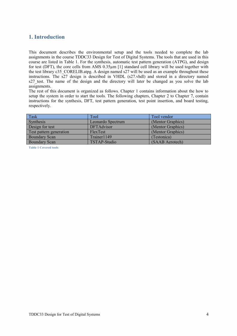
1. Introduction
This document describes the environmental setup and the tools needed to complete the lab assignments in the course TDDC33 Design for Test of Digital Systems. The tools that are used in this course are listed in Table 1. For the synthesis, automatic test pattern generation (ATPG), and design for test (DFT), the core cells from AMS 0.35µm [1] standard cell library will be used together with the test library c35_CORELIB.atpg. A design named s27 will be used as an example throughout these instructions. The s27 design is described in VHDL (s27.vhdl) and stored in a directory named s27_test. The name of the design and the directory will later be changed as you solve the lab assignments. The rest of this document is organized as follows. Chapter 1 contains information about the how to setup the system in order to start the tools. The following chapters, Chapter 2 to Chapter 7, contain instructions for the synthesis, DFT, test pattern generation, test point insertion, and board testing, respectively.
Task Tool Tool vendorSynthesis Leonardo Spectrum (Mentor Graphics)Design for test DFTAdvisor (Mentor Graphics)Test pattern generation FlexTest (Mentor Graphics)Boundary Scan Trainer1149 (Testonica)Boundary Scan TSTAP-Studio (SAAB Aerotech)Table 1 Covered tools
TDDC33 Design for Test of Digital Systems 4

2. Initial preparations
The following commands are all executed in a terminal window.
Add the modules /mentor/dft_2005 and mentor/fpgadv if they are missing.List the available loaded modules. module list
Add the modules. Note that the order of these commands is important. module add prog/mentor/dft_2005 module add prog/mentor/fpgadv
Note! Previously loaded mentor modules must be unloaded. If these modules are loaded by default at login, the login-file (.login) should be changed.
Make a directory s27_test mkdir s27_test
Download and extract the required files. (Described in the labs) Download the labx.tar.gz file where x is the number of the lab gunzip labx.tar.gz tar xvf labx.tar Copy the following files to the s27_test directory:
c35_CORELIB.atpg fflop.vhd gates.vhd s27.vhdl
Set the environment variable MODEL_TECH setenv MODEL_TECH /sw/mentor/fpgadv/6.2/Modeltech/bin
Generate the work directory $MODEL_TECH/vlib work
Compile the vhdl files $MODEL_TECH/vcom -93 fflop.vhd $MODEL_TECH/vcom -93 gates.vhd $MODEL_TECH/vcom s27.vhdl
TDDC33 Design for Test of Digital Systems 5
3. Synthesis
This chapter describes the synthesis procedure using Leonardo Spectrum from Mentor Graphics. It is assumed that the initial preparations, described in the Initial preparations, have been made.
3.1. InputA compiled VHDL-file
3.2. OutputA synthesized EDF-file
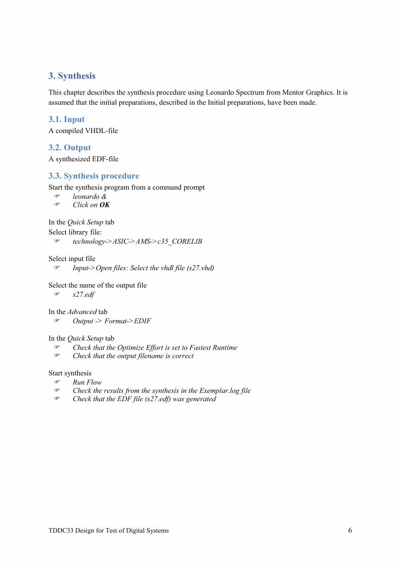
3.3. Synthesis procedureStart the synthesis program from a command prompt leonardo & Click on OK
In the Quick Setup tabSelect library file: technology->ASIC->AMS->c35_CORELIB
Select input file Input->Open files: Select the vhdl file (s27.vhd)
Select the name of the output file s27.edf
In the Advanced tab Output -> Format->EDIF
In the Quick Setup tab Check that the Optimize Effort is set to Fastest Runtime Check that the output filename is correct
Start synthesis Run Flow Check the results from the synthesis in the Exemplar.log file Check that the EDF file (s27.edf) was generated
TDDC33 Design for Test of Digital Systems 6
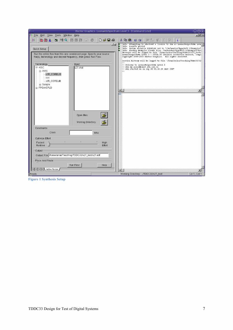
Figure 1 Synthesis Setup
TDDC33 Design for Test of Digital Systems 7
4. Design for test using DFTAdvisor This chapter describes how scan chain insertion is implemented using DFTAdvisor from Mentor Graphics.
4.1. Input A design netlist An ATPG library
4.2. Output A new design netlist Command file (do-file)
4.3. Starting DFTAdvisor Start the synthesis program from a command prompt dftadvisor &
In the DFTAdvisor Welcome window illustrated in Figure 2. Select the design Select the ATPG Library
Figure 2 DFTAdvisor Welcome Window
Click on Invoke DFTAdvisor DFTAdvisor has one command-based interface and one graphical interface. In this description we will mainly used the graphical interface, which is shown in Figure 3. The textual interface is useful for the verification of the results after the execution of commands.
TDDC33 Design for Test of Digital Systems 8
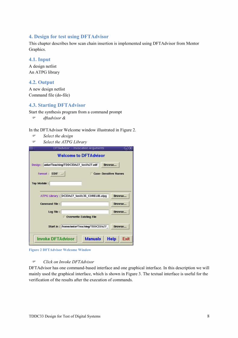
Figure 3 DFTAdvisor Control Panel
4.4. Circuit Setup
Specify the clocks in the Control Panel Click on Clocks
In the Setup Circuit Clocks window, illustrated in Figure 4. Check Manually Define Select the clock H and the Off-State 0 Click on Add Click on OK
Figure 4 Setup Circuit Clock window
In the Control Panel Click on DRC and Circuit Learning
TDDC33 Design for Test of Digital Systems 9
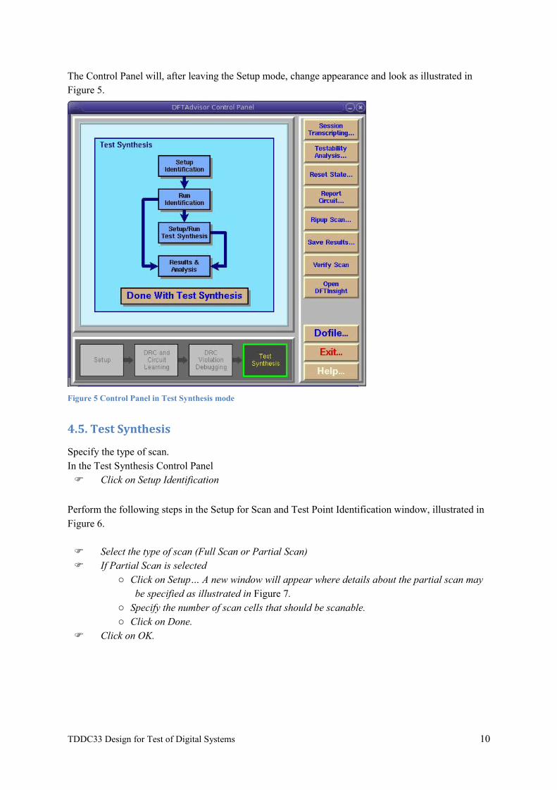
The Control Panel will, after leaving the Setup mode, change appearance and look as illustrated in Figure 5.
Figure 5 Control Panel in Test Synthesis mode
4.5. Test Synthesis
Specify the type of scan. In the Test Synthesis Control Panel Click on Setup Identification
Perform the following steps in the Setup for Scan and Test Point Identification window, illustrated in Figure 6.
Select the type of scan (Full Scan or Partial Scan) If Partial Scan is selected
o Click on Setup… A new window will appear where details about the partial scan may be specified as illustrated in Figure 7.
o Specify the number of scan cells that should be scanable. o Click on Done.
Click on OK.
TDDC33 Design for Test of Digital Systems 10
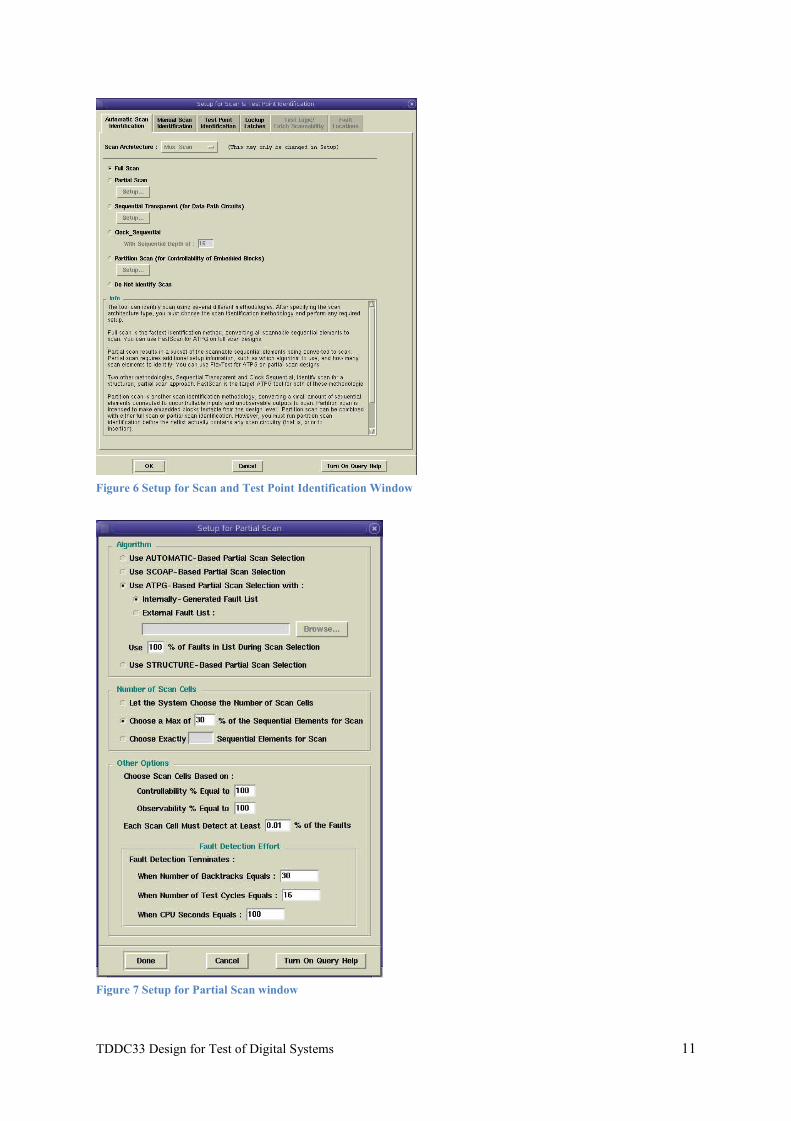
Figure 6 Setup for Scan and Test Point Identification Window
Figure 7 Setup for Partial Scan window
TDDC33 Design for Test of Digital Systems 11
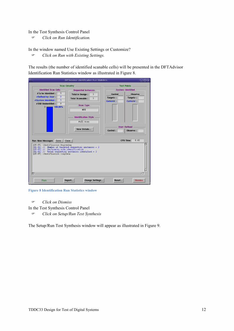
In the Test Synthesis Control Panel Click on Run Identification.
In the window named Use Existing Settings or Customize? Click on Run with Existing Settings.
The results (the number of identified scanable cells) will be presented in the DFTAdvisor Identification Run Statistics window as illustrated in Figure 8.
Figure 8 Identification Run Statistics window
Click on Dismiss In the Test Synthesis Control Panel Click on Setup/Run Test Synthesis
The Setup/Run Test Synthesis window will appear as illustrated in Figure 9.
TDDC33 Design for Test of Digital Systems 12
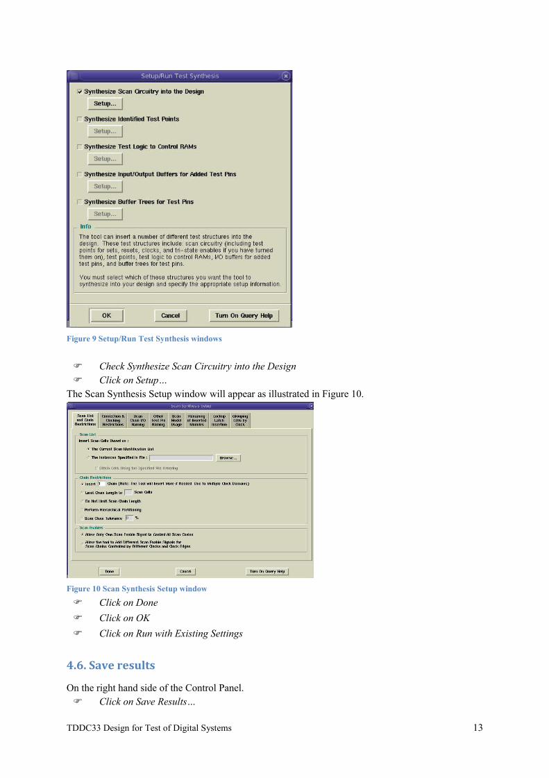
Figure 9 Setup/Run Test Synthesis windows
Check Synthesize Scan Circuitry into the Design Click on Setup…
The Scan Synthesis Setup window will appear as illustrated in Figure 10.
Figure 10 Scan Synthesis Setup window
Click on Done
Click on OK
Click on Run with Existing Settings
4.6. Save results
On the right hand side of the Control Panel. Click on Save Results…
TDDC33 Design for Test of Digital Systems 13
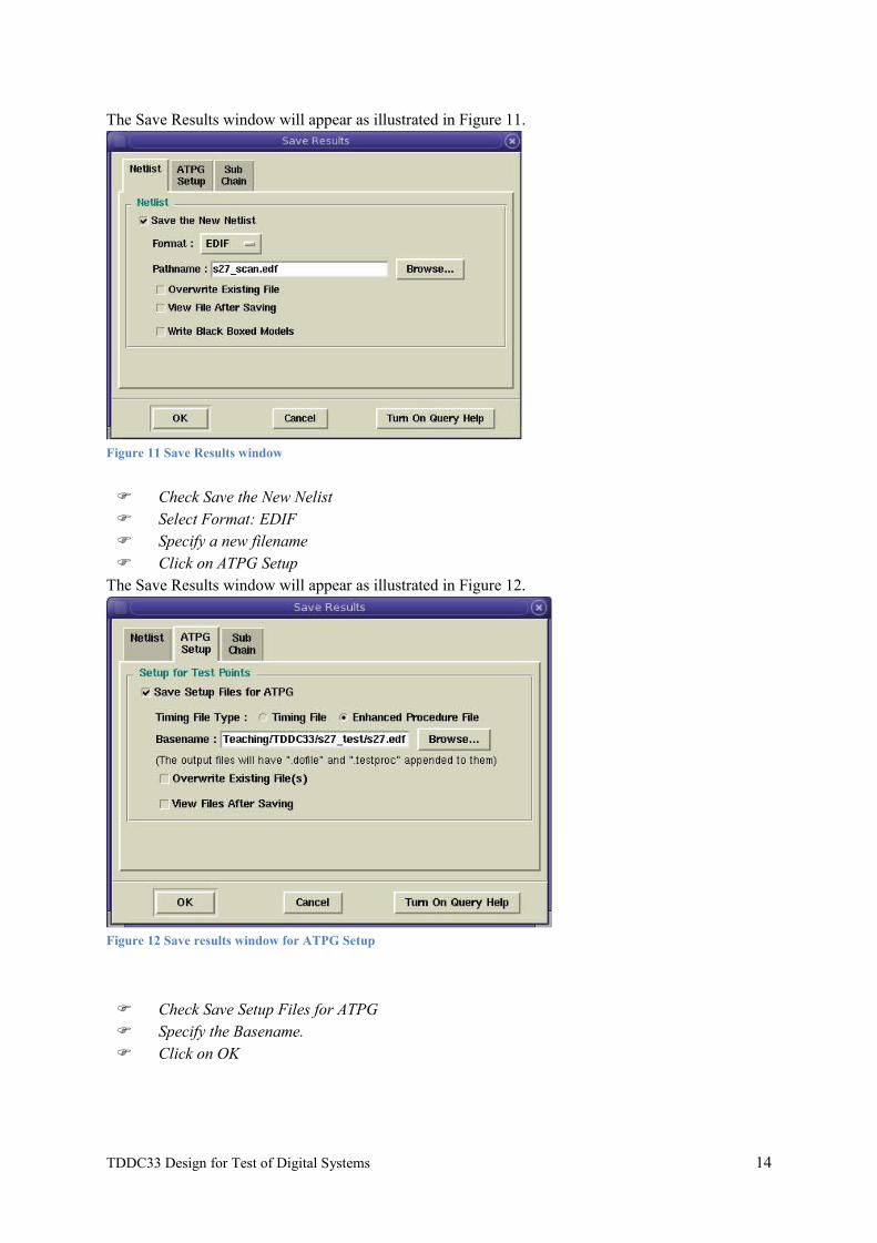
The Save Results window will appear as illustrated in Figure 11.
Figure 11 Save Results window
Check Save the New Nelist Select Format: EDIF Specify a new filename Click on ATPG Setup
The Save Results window will appear as illustrated in Figure 12.
Figure 12 Save results window for ATPG Setup
Check Save Setup Files for ATPG Specify the Basename. Click on OK
TDDC33 Design for Test of Digital Systems 14
5. Fault Coverage Analysis and Test Pattern Generation using FlexTest
This chapter describes the fault coverage analysis and test pattern generation process using FlexTest from Mentor Graphics. It is assumed that the initial preparations, described in Chapter 1, have been made.
5.1. Input
A design netlist An ATPG library External test patterns (optional) Command files; dofile and testproc file (optional)
5.2. Output
Test patterns Fault coverage
5.3. Writing test patterns
Manually crafted test patterns should be written in a text file using the following format:
• Combinational design (not the s27 design) SETUP =
TEST_CYCLE_WIDTH = 1; DECLARE INPUT BUS "ibus" = "/INP(0)", "/INP(1)", "/INP(2)",
"/INP(3)", "/INP(4)"; DECLARE OUTPUT BUS "obus" = "/OUTP(0)", "/OUTP(1)";
END; CYCLE_TEST =
PATTERN = 0; CYCLE = 0;
FORCE "ibus" "01100" 0; MEASURE "obus" "11" 1;
PATTERN = 1; CYCLE = 0;
FORCE "ibus" "10010" 0; MEASURE "obus" "00" 1;
END;
• Sequential design (could be the s27 design) SETUP =
TEST_CYCLE_WIDTH = 3; DECLARE INPUT BUS "ibus" = "/H", "/INP(0)", "/INP(1)", "/INP(2)",
"/INP(3)"; DECLARE OUTPUT BUS "obus_3" = "/OUTP(0)"; CLOCK "/H" =
TDDC33 Design for Test of Digital Systems 15
OFF_STATE = 0; END;
END; CYCLE_TEST =
CYCLE = 0; FORCE "ibus" "01111" 0; FORCE "ibus" "11111" 1; FORCE "ibus" "01111" 2; MEASURE "obus_3" "1" 3;
CYCLE = 1; FORCE "ibus" "01100" 0; FORCE "ibus" "11100" 1; FORCE "ibus" "01100" 2; MEASURE "obus_3" "1" 3;
END;
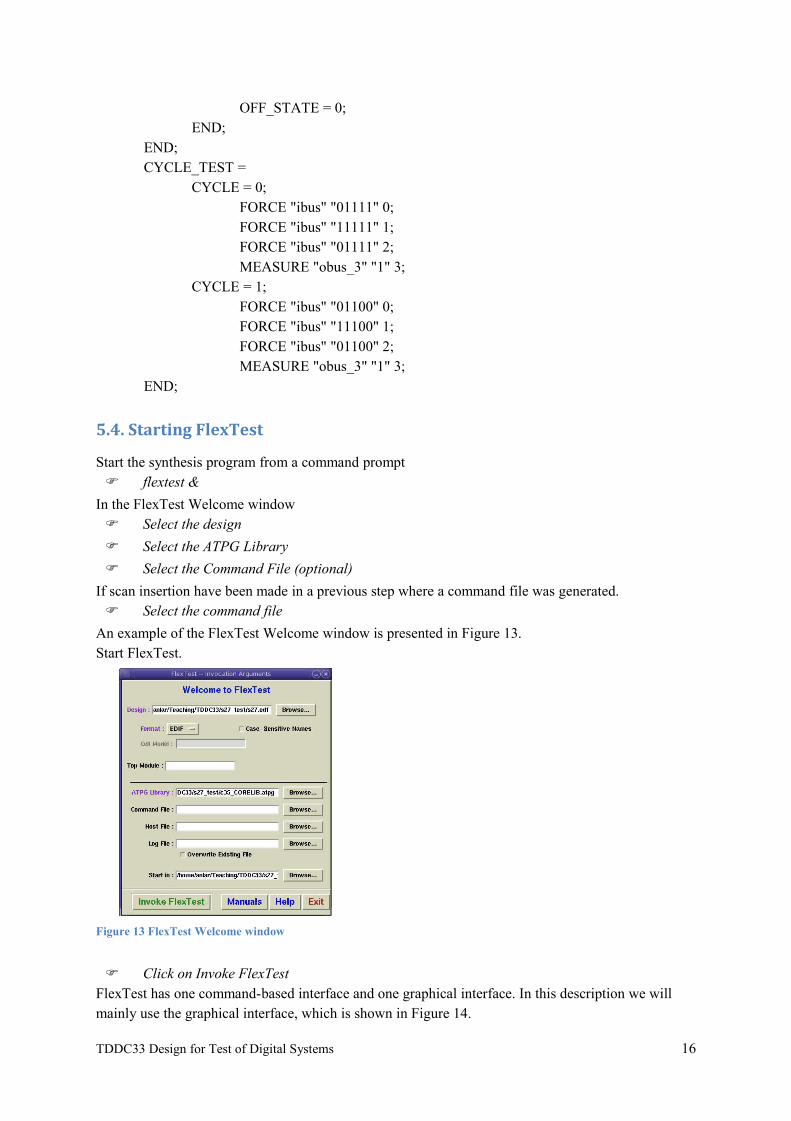
5.4. Starting FlexTest
Start the synthesis program from a command prompt flextest &
In the FlexTest Welcome window Select the design
Select the ATPG Library
Select the Command File (optional)
If scan insertion have been made in a previous step where a command file was generated. Select the command file
An example of the FlexTest Welcome window is presented in Figure 13. Start FlexTest.
Figure 13 FlexTest Welcome window
Click on Invoke FlexTest FlexTest has one command-based interface and one graphical interface. In this description we will mainly use the graphical interface, which is shown in Figure 14.
TDDC33 Design for Test of Digital Systems 16
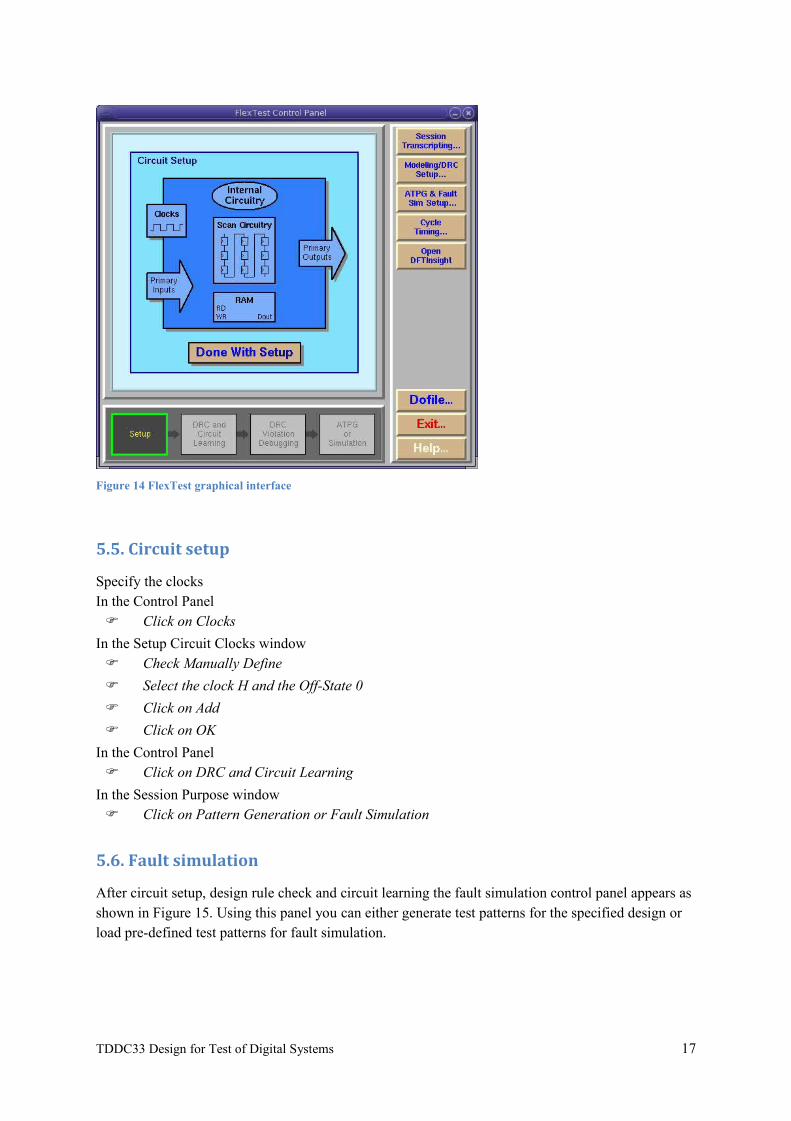
Figure 14 FlexTest graphical interface
5.5. Circuit setup
Specify the clocks In the Control Panel Click on Clocks
In the Setup Circuit Clocks window Check Manually Define
Select the clock H and the Off-State 0
Click on Add
Click on OK
In the Control Panel Click on DRC and Circuit Learning
In the Session Purpose window Click on Pattern Generation or Fault Simulation
5.6. Fault simulation
After circuit setup, design rule check and circuit learning the fault simulation control panel appears as shown in Figure 15. Using this panel you can either generate test patterns for the specified design or load pre-defined test patterns for fault simulation.
TDDC33 Design for Test of Digital Systems 17
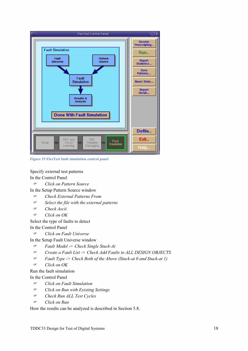
Figure 15 FlexTest fault simulation control panel
Specify external test patterns In the Control Panel Click on Pattern Source
In the Setup Pattern Source window Check External Patterns From Select the file with the external patterns Check Ascii Click on OK
Select the type of faults to detect In the Control Panel Click on Fault Universe
In the Setup Fault Universe window Fault Model -> Check Single Stuck-At Create a Fault List -> Check Add Faults to ALL DESIGN OBJECTS Fault Type -> Check Both of the Above (Stuck-at 0 and Stuck-at 1) Click on OK
Run the fault simulation In the Control Panel Click on Fault Simulation Click on Run with Existing Settings Check Run ALL Test Cycles Click on Run
How the results can be analyzed is described in Section 5.8.
TDDC33 Design for Test of Digital Systems 18
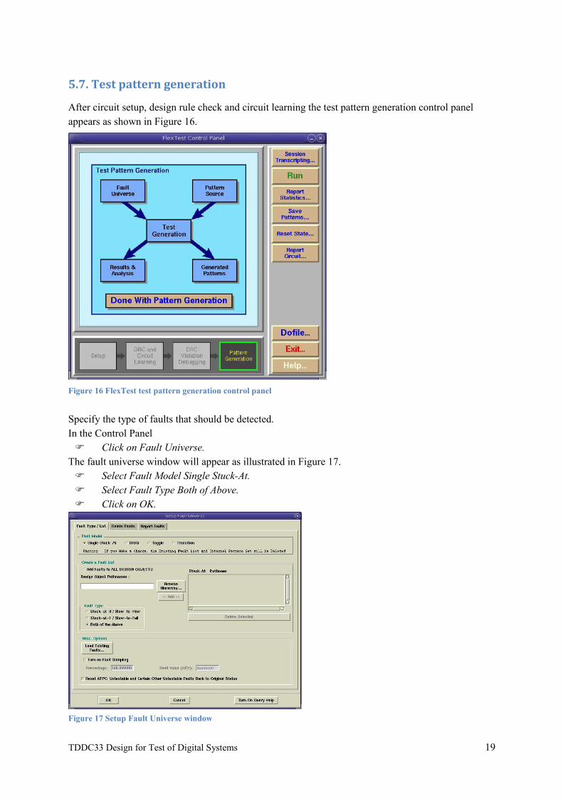
5.7. Test pattern generation
After circuit setup, design rule check and circuit learning the test pattern generation control panel appears as shown in Figure 16.
Figure 16 FlexTest test pattern generation control panel
Specify the type of faults that should be detected. In the Control Panel Click on Fault Universe.
The fault universe window will appear as illustrated in Figure 17. Select Fault Model Single Stuck-At. Select Fault Type Both of Above. Click on OK.
Figure 17 Setup Fault Universe window
TDDC33 Design for Test of Digital Systems 19
Run the test pattern generation. Click on Test Generation. Click on Run with Existing Settings. Click on Add All Faults.
The results will be presented in the FlextTest Run ATPG Run Statistics window. How the results can be analyzed in described in Section 5.8.
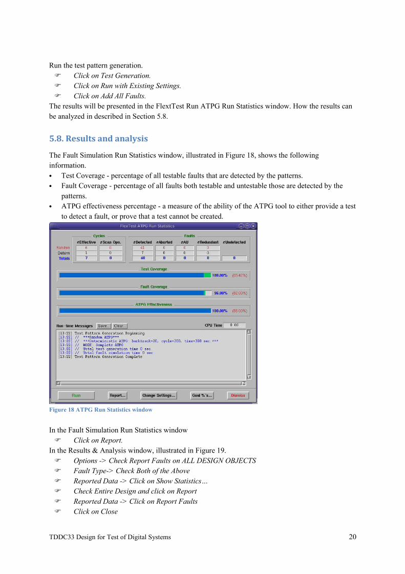
5.8. Results and analysis
The Fault Simulation Run Statistics window, illustrated in Figure 18, shows the following information.
• Test Coverage - percentage of all testable faults that are detected by the patterns.
• Fault Coverage - percentage of all faults both testable and untestable those are detected by the patterns.
• ATPG effectiveness percentage - a measure of the ability of the ATPG tool to either provide a test to detect a fault, or prove that a test cannot be created.
Figure 18 ATPG Run Statistics window
In the Fault Simulation Run Statistics window Click on Report.
In the Results & Analysis window, illustrated in Figure 19. Options -> Check Report Faults on ALL DESIGN OBJECTS Fault Type-> Check Both of the Above Reported Data -> Click on Show Statistics… Check Entire Design and click on Report Reported Data -> Click on Report Faults Click on Close
TDDC33 Design for Test of Digital Systems 20
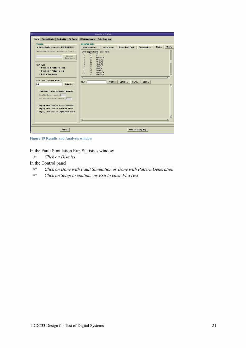
Figure 19 Results and Analysis window
In the Fault Simulation Run Statistics window Click on Dismiss
In the Control panel Click on Done with Fault Simulation or Done with Pattern Generation Click on Setup to continue or Exit to close FlexTest
TDDC33 Design for Test of Digital Systems 21
6. Test point insertion in VHDL
This chapter describes how the testability of a design can be improved by inserting test points. It is assumed that the VHDL description of a design is available.
6.1. Input
A design described in VHDL
6.2. Output
A new design with test points.
6.3. Inserting test points
Add the new input and output ports in the ENTITY block
Add new signals in the ARCHITECTURE block (if needed)
Modify the design (introduction of new gates may be required) such that the new ports is used
to control and observe the “hard-to-test” parts of the design.
Please refer to Appendix A for an example of VHDL code with inserted test points.
TDDC33 Design for Test of Digital Systems 22

7. Board test using Boundary Scan (IEEE 1149.1)
This chapter describes the boundary scan board test methodology. For the board test programming and test, a program called Trainer1149 from Testonica Lab is used.
7.1. Input
A board design, consisting of one bsdl-file for each chip together with a list of connections.
7.2. Output
A test program.
7.3. Starting Trainer1149
Verify that the current installed version of java is 1.6 or higher java –version
module add prog/jdk/1.6
Start the Trainer1149 program java –jar trainer1149.jar &
Select an existing project or make a new project
7.4. How to use Trainer1149
The Trainer1149 program has three different modes, Project Mode, Debug Mode, and Board Edit Mode. The Trainer1149 program will start in the project mode, which allows you to view and modify the board layout. In Figure 20, the twochips.nl netlist has been chosen in the Project Explorer.
TDDC33 Design for Test of Digital Systems 23
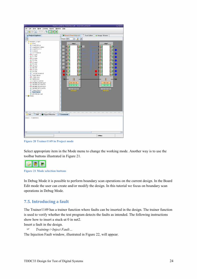
Figure 20 Trainer1149 in Project mode
Select appropriate item in the Mode menu to change the working mode. Another way is to use the toolbar buttons illustrated in Figure 21.
Figure 21 Mode selection buttons
In Debug Mode it is possible to perform boundary scan operations on the current design. In the Board Edit mode the user can create and/or modify the design. In this tutorial we focus on boundary scan operations in Debug Mode.
7.5. Introducing a fault
The Trainer1149 has a trainer function where faults can be inserted in the design. The trainer function is used to verify whether the test program detects the faults as intended. The following instructions show how to insert a stuck-at 0 in net2. Insert a fault in the design. Training->Inject Fault…
The Injection Fault window, illustrated in Figure 22, will appear.
TDDC33 Design for Test of Digital Systems 24
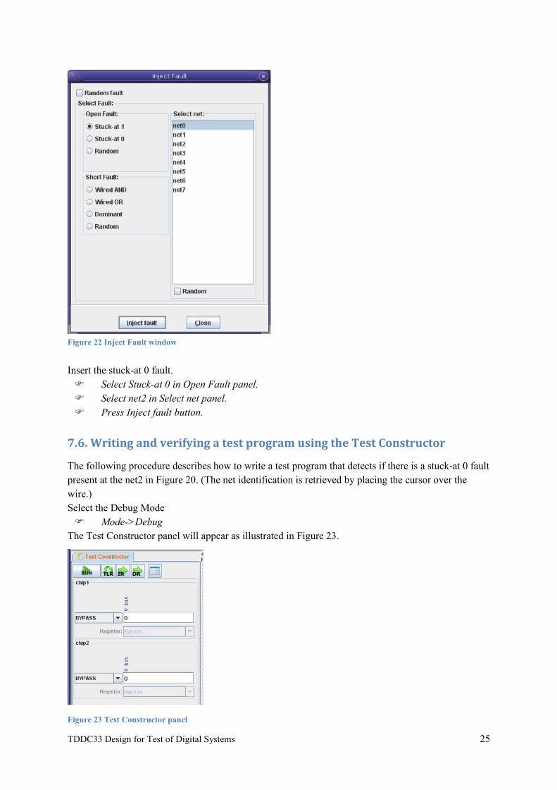
Figure 22 Inject Fault window
Insert the stuck-at 0 fault. Select Stuck-at 0 in Open Fault panel. Select net2 in Select net panel. Press Inject fault button.
7.6. Writing and verifying a test program using the Test Constructor
The following procedure describes how to write a test program that detects if there is a stuck-at 0 fault present at the net2 in Figure 20. (The net identification is retrieved by placing the cursor over the wire.) Select the Debug Mode Mode->Debug
The Test Constructor panel will appear as illustrated in Figure 23.
Figure 23 Test Constructor panel
TDDC33 Design for Test of Digital Systems 25
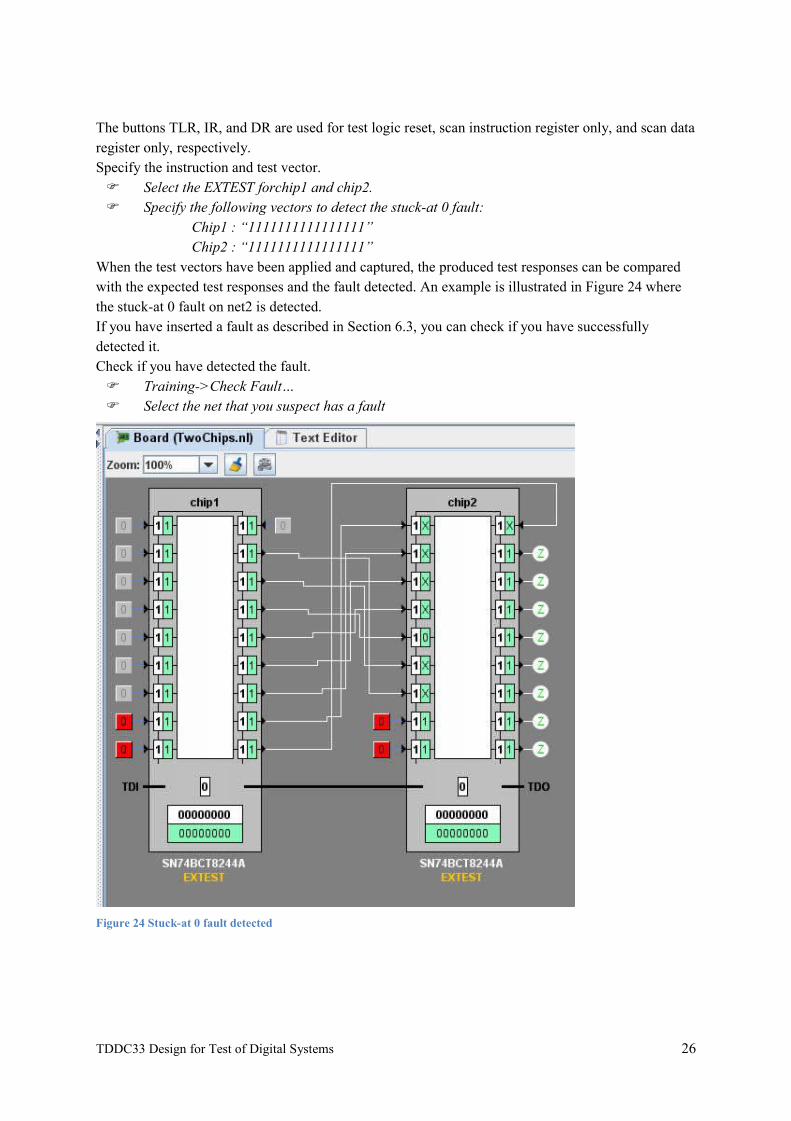
The buttons TLR, IR, and DR are used for test logic reset, scan instruction register only, and scan data register only, respectively. Specify the instruction and test vector. Select the EXTEST forchip1 and chip2. Specify the following vectors to detect the stuck-at 0 fault:
Chip1 : “1111111111111111” Chip2 : “1111111111111111”
When the test vectors have been applied and captured, the produced test responses can be compared with the expected test responses and the fault detected. An example is illustrated in Figure 24 where the stuck-at 0 fault on net2 is detected. If you have inserted a fault as described in Section 6.3, you can check if you have successfully detected it. Check if you have detected the fault. Training->Check Fault… Select the net that you suspect has a fault
Figure 24 Stuck-at 0 fault detected
TDDC33 Design for Test of Digital Systems 26
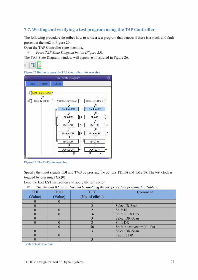
7.7. Writing and verifying a test program using the TAP Controller
The following procedure describes how to write a test program that detects if there is a stuck-at 0 fault present at the net2 in Figure 20. Open the TAP Controller state machine. Press TAP State Diagram button (Figure 25).
The TAP State Diagram window will appear as illustrated in Figure 26.
Figure 25 Button to open the TAP Controller state machine
Figure 26 The TAP state machine
Specify the input signals TDI and TMS by pressing the buttons TDI(0) and TMS(0). The test clock is toggled by pressing TCK(0). Load the EXTEST instruction and apply the test vector. The stuck-at 0 fault is detected by applying the test procedure presented in Table 2.
TDI(Value)
TDO(Value)
TCK(No. of clicks)
Comment
0 0 10 1 2 Select IR-Scan0 0 2 Shift-IR0 0 16 Shift in EXTEST0 1 3 Select DR-Scan0 0 2 Shift-DR1 0 36 Shift in test vector (all 1’s)0 1 3 Select DR-Scan0 0 1 Capture DR0 1 3
Table 2 Test procedure
TDDC33 Design for Test of Digital Systems 27
8.Board Testing using Boundary Scan (IEEE 1149.1)
For the purpose of board testing using Boundary Scan in TDDC33 we will use the TSTAP-Studio software provided by SAAB Aerotech. TSTAP-Studio contains two useful tools TSTAP-PG and TSTAP-RT.TSTAP-PG is a tool for automatic test pattern generation. It uses a node list file in order to generate test vectors which are later used by TSTAP-RT tool which runs the tests and determines whether the test passes or fails. In the following text we give a description how to use the TSTAP-Studio
8.1 Create new project
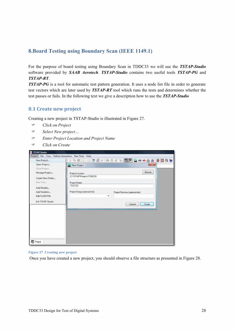
Creating a new project in TSTAP-Studio is illustrated in Figure 27.
Click on Project
Select New project…
Enter Project Location and Project Name
Click on Create
Figure 27 Creating new project
Once you have created a new project, you should observe a file structure as presented in Figure 28.
TDDC33 Design for Test of Digital Systems 28
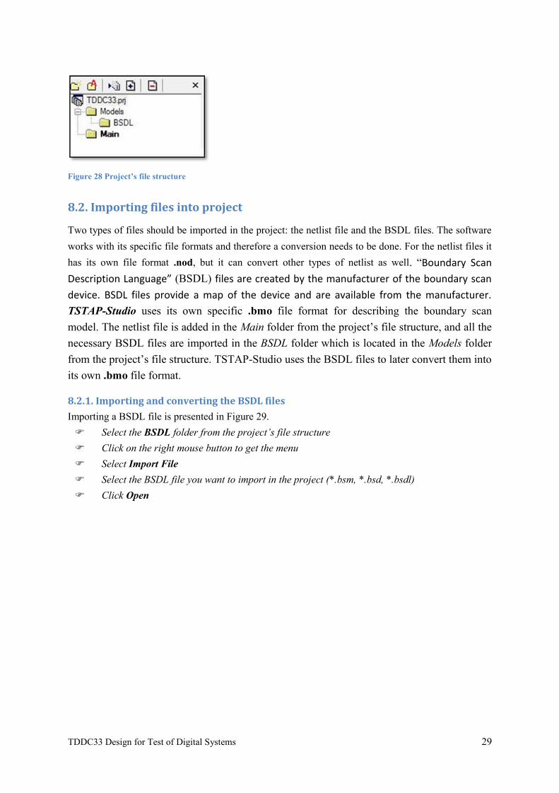
Figure 28 Project’s file structure
8.2. Importing files into project
Two types of files should be imported in the project: the netlist file and the BSDL files. The software
works with its specific file formats and therefore a conversion needs to be done. For the netlist files it
has its own file format .nod, but it can convert other types of netlist as well. “Boundary Scan Description Language” (BSDL) files are created by the manufacturer of the boundary scan
device. BSDL files provide a map of the device and are available from the manufacturer. TSTAP-Studio uses its own specific .bmo file format for describing the boundary scan
model. The netlist file is added in the Main folder from the project’s file structure, and all the
necessary BSDL files are imported in the BSDL folder which is located in the Models folder
from the project’s file structure. TSTAP-Studio uses the BSDL files to later convert them into
its own .bmo file format.
8.2.1. Importing and converting the BSDL files
Importing a BSDL file is presented in Figure 29.
Select the BSDL folder from the project’s file structure
Click on the right mouse button to get the menu
Select Import File
Select the BSDL file you want to import in the project (*.bsm, *.bsd, *.bsdl)
Click Open
TDDC33 Design for Test of Digital Systems 29
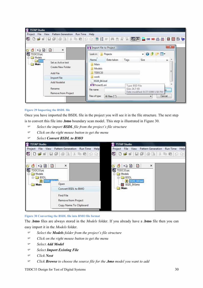
Figure 29 Importing the BSDL file
Once you have imported the BSDL file in the project you will see it in the file structure. The next step
is to convert this file into .bmo boundary scan model. This step is illustrated in Figure 30.
Select the import BSDL file from the project’s file structure
Click on the right mouse button to get the menu
Select Convert BSDL to BMO
Figure 30 Converting the BSDL file into BMO file format
The .bmo files are always stored in the Models folder. If you already have a .bmo file then you can
easy import it in the Models folder.
Select the Models folder from the project’s file structure
Click on the right mouse button to get the menu
Select Add Model
Select Import Existing File
Click Next
Click Browse to choose the source file for the .bmo model you want to add
TDDC33 Design for Test of Digital Systems 30
Set Destination Test to be Models
Click Finish
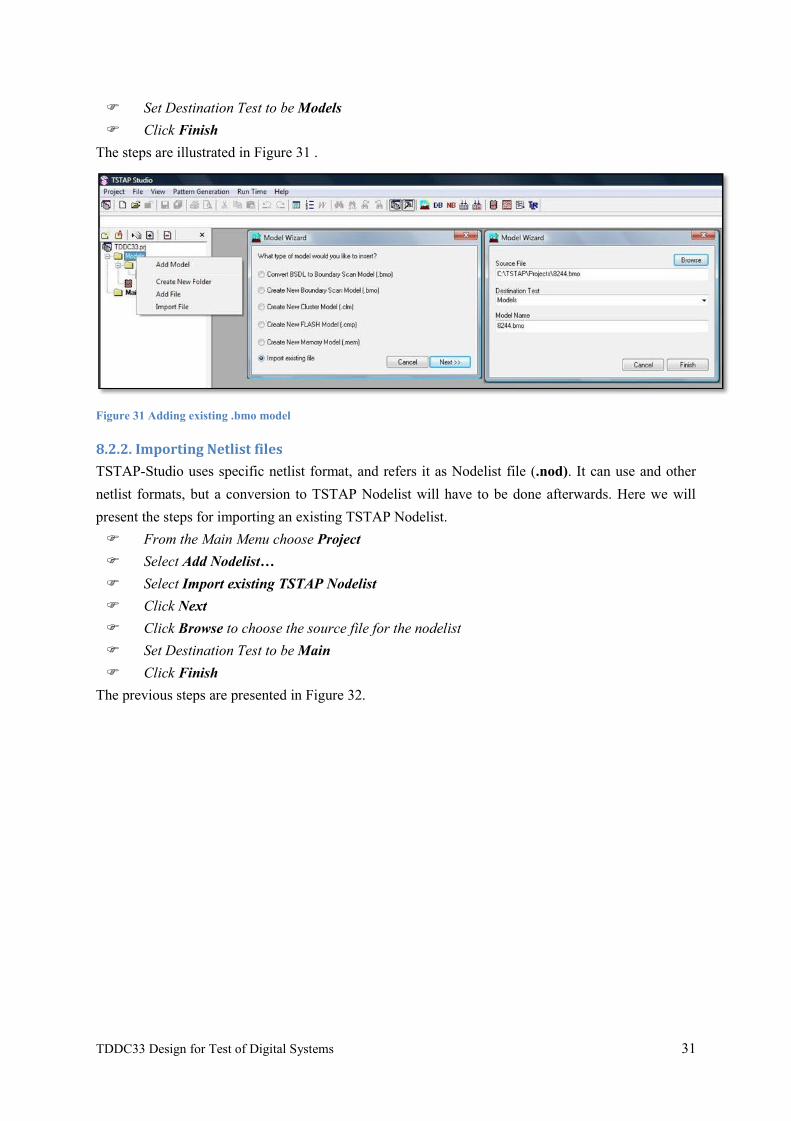
The steps are illustrated in Figure 31 .
Figure 31 Adding existing .bmo model
8.2.2. Importing Netlist files
TSTAP-Studio uses specific netlist format, and refers it as Nodelist file (.nod). It can use and other
netlist formats, but a conversion to TSTAP Nodelist will have to be done afterwards. Here we will
present the steps for importing an existing TSTAP Nodelist.
From the Main Menu choose Project
Select Add Nodelist…
Select Import existing TSTAP Nodelist
Click Next
Click Browse to choose the source file for the nodelist
Set Destination Test to be Main
Click Finish
The previous steps are presented in Figure 32.
TDDC33 Design for Test of Digital Systems 31
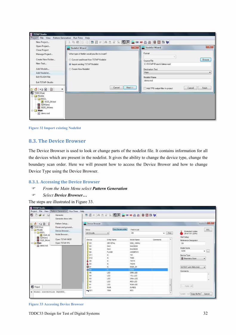
Figure 32 Import existing Nodelist
8.3. The Device Browser
The Device Browser is used to look or change parts of the nodelist file. It contains information for all
the devices which are present in the nodelist. It gives the ability to change the device type, change the
boundary scan order. Here we will present how to access the Device Brower and how to change
Device Type using the Device Browser.
8.3.1. Accessing the Device Browser
From the Main Menu select Pattern Generation
Select Device Browser…
The steps are illustrated in Figure 33.
Figure 33 Accessing Device Browser
TDDC33 Design for Test of Digital Systems 32
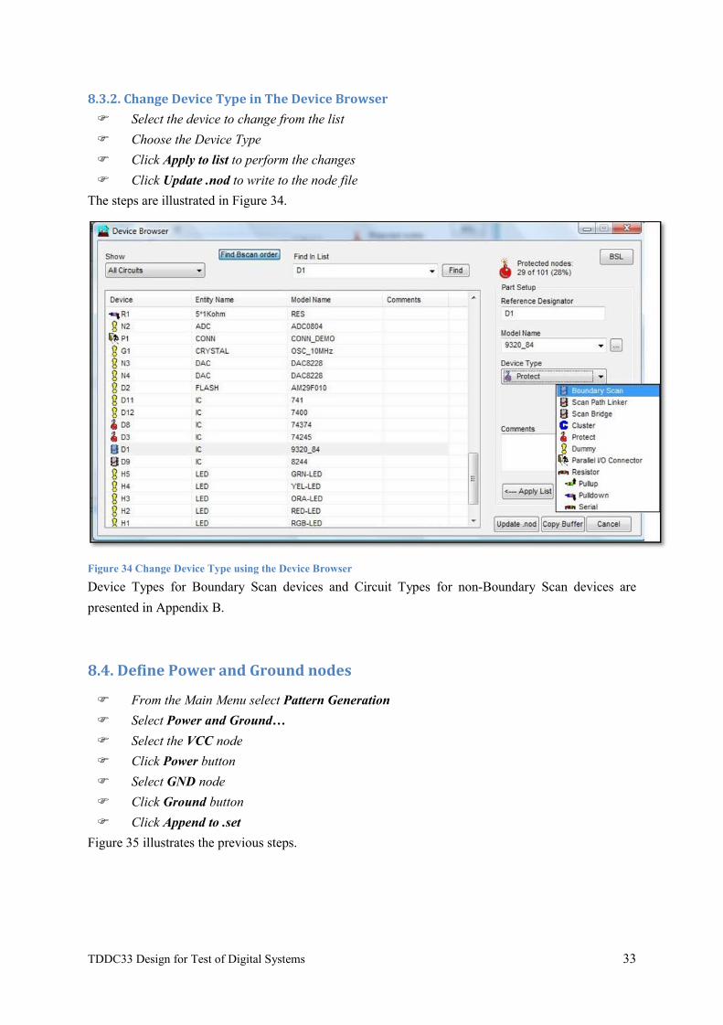
8.3.2. Change Device Type in The Device Browser
Select the device to change from the list
Choose the Device Type
Click Apply to list to perform the changes
Click Update .nod to write to the node file
The steps are illustrated in Figure 34.
Figure 34 Change Device Type using the Device Browser
Device Types for Boundary Scan devices and Circuit Types for non-Boundary Scan devices are
presented in Appendix B.
8.4. Define Power and Ground nodes
From the Main Menu select Pattern Generation
Select Power and Ground…
Select the VCC node
Click Power button
Select GND node
Click Ground button
Click Append to .set
Figure 35 illustrates the previous steps.
TDDC33 Design for Test of Digital Systems 33
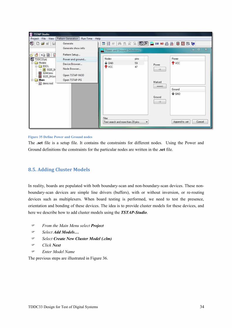
Figure 35 Define Power and Ground nodes
The .set file is a setup file. It contains the constraints for different nodes. Using the Power and
Ground definitions the constraints for the particular nodes are written in the .set file.
8.5. Adding Cluster Models
In reality, boards are populated with both boundary-scan and non-boundary-scan devices. These non-
boundary-scan devices are simple line drivers (buffers), with or without inversion, or re-routing
devices such as multiplexers. When board testing is performed, we need to test the presence,
orientation and bonding of these devices. The idea is to provide cluster models for these devices, and
here we describe how to add cluster models using the TSTAP-Studio.
From the Main Menu select Project
Select Add Models…
Select Create New Cluster Model (.clm)
Click Next
Enter Model Name
The previous steps are illustrated in Figure 36.
TDDC33 Design for Test of Digital Systems 34
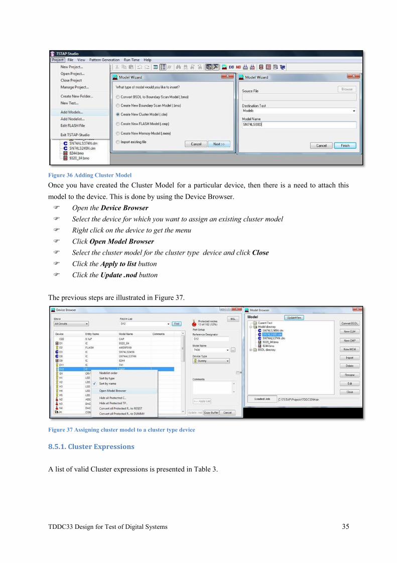
Figure 36 Adding Cluster Model
Once you have created the Cluster Model for a particular device, then there is a need to attach this
model to the device. This is done by using the Device Browser.
Open the Device Browser
Select the device for which you want to assign an existing cluster model
Right click on the device to get the menu
Click Open Model Browser
Select the cluster model for the cluster type device and click Close
Click the Apply to list button
Click the Update .nod button
The previous steps are illustrated in Figure 37.
Figure 37 Assigning cluster model to a cluster type device
8.5.1. Cluster Expressions
A list of valid Cluster expressions is presented in Table 3.
TDDC33 Design for Test of Digital Systems 35

Used on cluster inputsDRIVE Boundary scan pin on this node will driveSENSE Boundary scan pin on this node will senseFOLLOW One signal follows another oneCLOCK A toggling signal is driven
Used for describing cluster outputsEQUAL Outputs same logical value as inputCLK_EQUAL Outputs same logical value as input, but next test vector
Boolean$ Negate* Logical ANDTable 3 Cluster Expressions
An example of defining a cluster model is presented in Appendix C.
8.5.3. Cluster levels
If there are several cluster type devices that may drive a boundary-scan node, then there is a need to
specify different cluster levels. Usually in this case cluster models include parts, such that the device
is either enabled or disabled. This enable/disable control must come from a boundary-scan cell. In the
following part we present how to add different cluster levels. It is important that the situations where
multiple cluster devices are driving at the same time (clash) should be avoided in all the cluster levels.
Usually in the first cluster level the cluster devices should be disabled.
Open the Device Browser
From the dropdown list, select to show only the cluster circuits
Select a cluster device
Right click on the device to get the menu
Select Add Section sec_name, if you want to add the particular section (some mode of
behavior of the component, enable/disable for example) in the consequent cluster level
Select Delete last section, if you want to remove the last section from the last cluster level for
the selected device
Figure 38 illustrates these steps.
TDDC33 Design for Test of Digital Systems 36
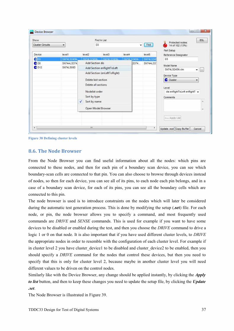
Figure 38 Defining cluster levels
8.6. The Node Browser
From the Node Browser you can find useful information about all the nodes: which pins are
connected to these nodes, and then for each pin of a boundary scan device, you can see which
boundary-scan cells are connected to that pin. You can also choose to browse through devices instead
of nodes, so then for each device, you can see all of its pins, to each node each pin belongs, and in a
case of a boundary scan device, for each of its pins, you can see all the boundary cells which are
connected to this pin.
The node browser is used is to introduce constraints on the nodes which will later be considered
during the automatic test generation process. This is done by modifying the setup (.set) file. For each
node, or pin, the node browser allows you to specify a command, and most frequently used
commands are DRIVE and SENSE commands. This is used for example if you want to have some
devices to be disabled or enabled during the test, and then you choose the DRIVE command to drive a
logic 1 or 0 on that node. It is also important that if you have used different cluster levels, to DRIVE
the appropriate nodes in order to resemble with the configuration of each cluster level. For example if
in cluster level 2 you have cluster_device1 to be disabled and cluster_device2 to be enabled, then you
should specify a DRIVE command for the nodes that control these devices, but then you need to
specify that this is only for cluster level 2, because maybe in another cluster level you will need
different values to be driven on the control nodes.
Similarly like with the Device Browser, any change should be applied instantly, by clicking the Apply
to list button, and then to keep these changes you need to update the setup file, by clicking the Update
.set.
The Node Browser is illustrated in Figure 39.
TDDC33 Design for Test of Digital Systems 37
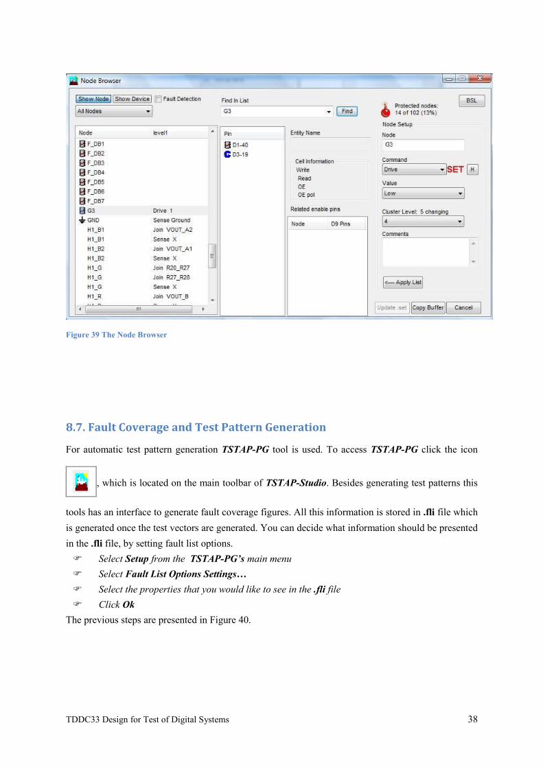
Figure 39 The Node Browser
8.7. Fault Coverage and Test Pattern Generation
For automatic test pattern generation TSTAP-PG tool is used. To access TSTAP-PG click the icon
, which is located on the main toolbar of TSTAP-Studio. Besides generating test patterns this
tools has an interface to generate fault coverage figures. All this information is stored in .fli file which
is generated once the test vectors are generated. You can decide what information should be presented
in the .fli file, by setting fault list options.
Select Setup from the TSTAP-PG’s main menu
Select Fault List Options Settings…
Select the properties that you would like to see in the .fli file
Click Ok
The previous steps are presented in Figure 40.
TDDC33 Design for Test of Digital Systems 38
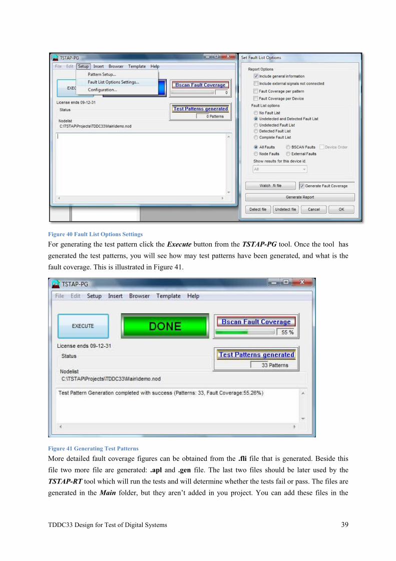
Figure 40 Fault List Options Settings
For generating the test pattern click the Execute button from the TSTAP-PG tool. Once the tool has
generated the test patterns, you will see how may test patterns have been generated, and what is the
fault coverage. This is illustrated in Figure 41.
Figure 41 Generating Test Patterns
More detailed fault coverage figures can be obtained from the .fli file that is generated. Beside this
file two more file are generated: .apl and .gen file. The last two files should be later used by the
TSTAP-RT tool which will run the tests and will determine whether the tests fail or pass. The files are
generated in the Main folder, but they aren’t added in you project. You can add these files in the
TDDC33 Design for Test of Digital Systems 39
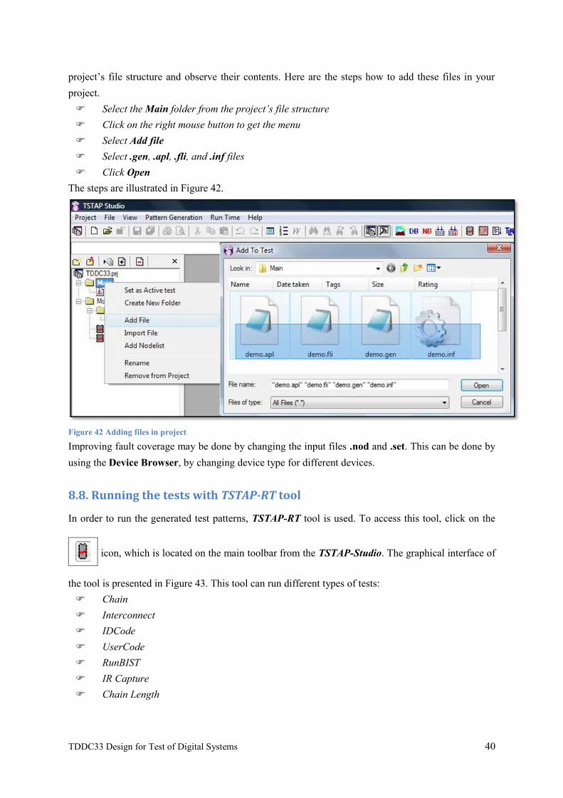
project’s file structure and observe their contents. Here are the steps how to add these files in your
project.
Select the Main folder from the project’s file structure
Click on the right mouse button to get the menu
Select Add file
Select .gen, .apl, .fli, and .inf files
Click Open
The steps are illustrated in Figure 42.
Figure 42 Adding files in project
Improving fault coverage may be done by changing the input files .nod and .set. This can be done by
using the Device Browser, by changing device type for different devices.
8.8. Running the tests with TSTAP-RT tool
In order to run the generated test patterns, TSTAP-RT tool is used. To access this tool, click on the
icon, which is located on the main toolbar from the TSTAP-Studio. The graphical interface of
the tool is presented in Figure 43. This tool can run different types of tests:
Chain
Interconnect
IDCode
UserCode
RunBIST
IR Capture
Chain Length
TDDC33 Design for Test of Digital Systems 40
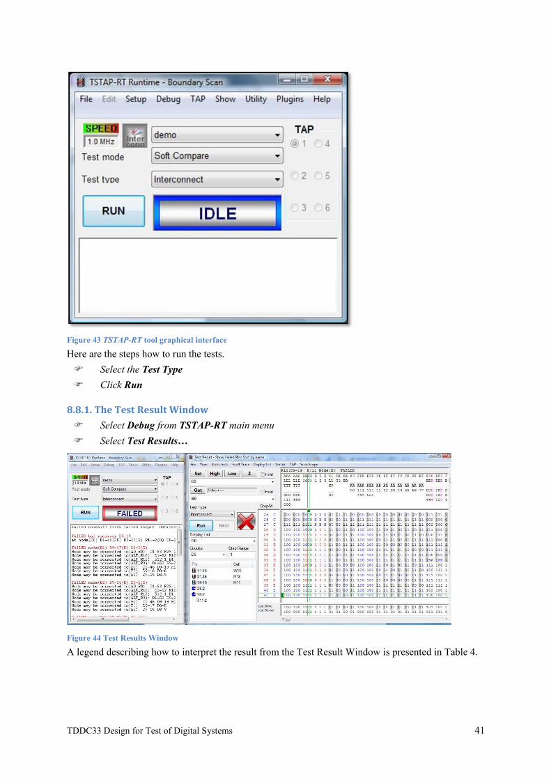
Figure 43 TSTAP-RT tool graphical interface
Here are the steps how to run the tests.
Select the Test Type
Click Run
8.8.1. The Test Result Window
Select Debug from TSTAP-RT main menu
Select Test Results…
Figure 44 Test Results Window
A legend describing how to interpret the result from the Test Result Window is presented in Table 4.
TDDC33 Design for Test of Digital Systems 41
Failed steps and signals are red. The shown value is the expected valuePassed steps and signals are blueDriver signals are blackActive driver has grey backgroundCluster driver is lilacTable 4 Interpreting the results from the Test Result Window
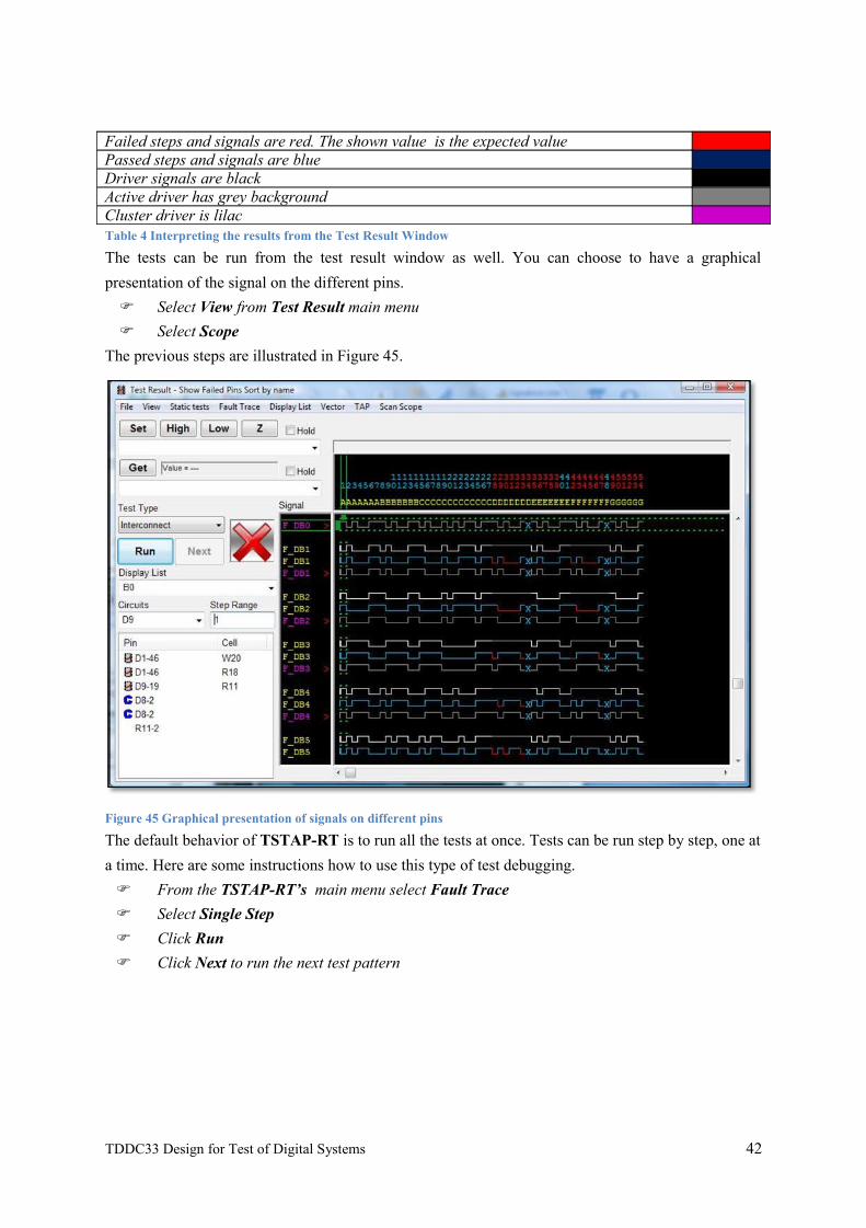
The tests can be run from the test result window as well. You can choose to have a graphical
presentation of the signal on the different pins.
Select View from Test Result main menu
Select Scope
The previous steps are illustrated in Figure 45.
Figure 45 Graphical presentation of signals on different pins
The default behavior of TSTAP-RT is to run all the tests at once. Tests can be run step by step, one at
a time. Here are some instructions how to use this type of test debugging.
From the TSTAP-RT’s main menu select Fault Trace
Select Single Step
Click Run
Click Next to run the next test pattern
TDDC33 Design for Test of Digital Systems 42
8.9. Working with BSL (Boundary scan Stimuli Language) files
BSL is not a standard “high-level” language, but instead it is an in-house (SAAB) language for "high-
level" test of Boundary-Scan devices.
BSL files are used for testing complex devices on the board, focusing mainly on non-boundary-scan
devices that are interconnected with boundary-scan devices. Here we will present a brief description
of a proper BSL file.
A BSL file consists of several parts:
• VECTOR DEFINITIONS
• MACRO DEFINITIONS
• PIN DEFINITIONS
• DEFAULT DEFINTIONS
• STIMULI SECTION
A test designer should only focus on the MACRO DEFINITIONS and STIMULI SECTION, the other
skeleton of the BSL file is automatically generated from the software when creating the BSL file. The
test patterns are part of the STIMULI SECTION, and ‘$’ is used to separate the different test patterns.
The use of MACRO DEFINITIONS can reduce the size of the BSL file, especially when the test
patterns that you want to generate follow a certain scheme. In that case you simply write a macro
definition and by using parameter list, you describe the scheme how the test patterns should be
generated. Once you have written the macro definition, it can be used in the STIMULI SECTION.
The PIN DEFINITIONS part is automatically generated. The pin definition syntax is as follow:
put pin_name[device_name-device_pin_number.boundary_scan_cell_number];for output pins
or
get pin_name[device_name-device_pin_number.boundary_scan_cell_number];for input pins
Because usually control boundary-scan cells for an I/O pins are not connected to a physical pin of the
boundary-scan device, in those cases device_pin_number is replaced with an ‘*’ character.
The VECTOR DEFINITIONS part is automatically generated as well. The vector definition syntax is:
VECTOR vector_name = pin_name1,pin_name2, . . . pin_namen;
In the STIMULI SECTION you are writing the test patterns. The test patterns consist of assigning
values to pins or vectors. You can as well use arithmetic and logic expressions for vectors.
• Assigning values to pins:
TDDC33 Design for Test of Digital Systems 43
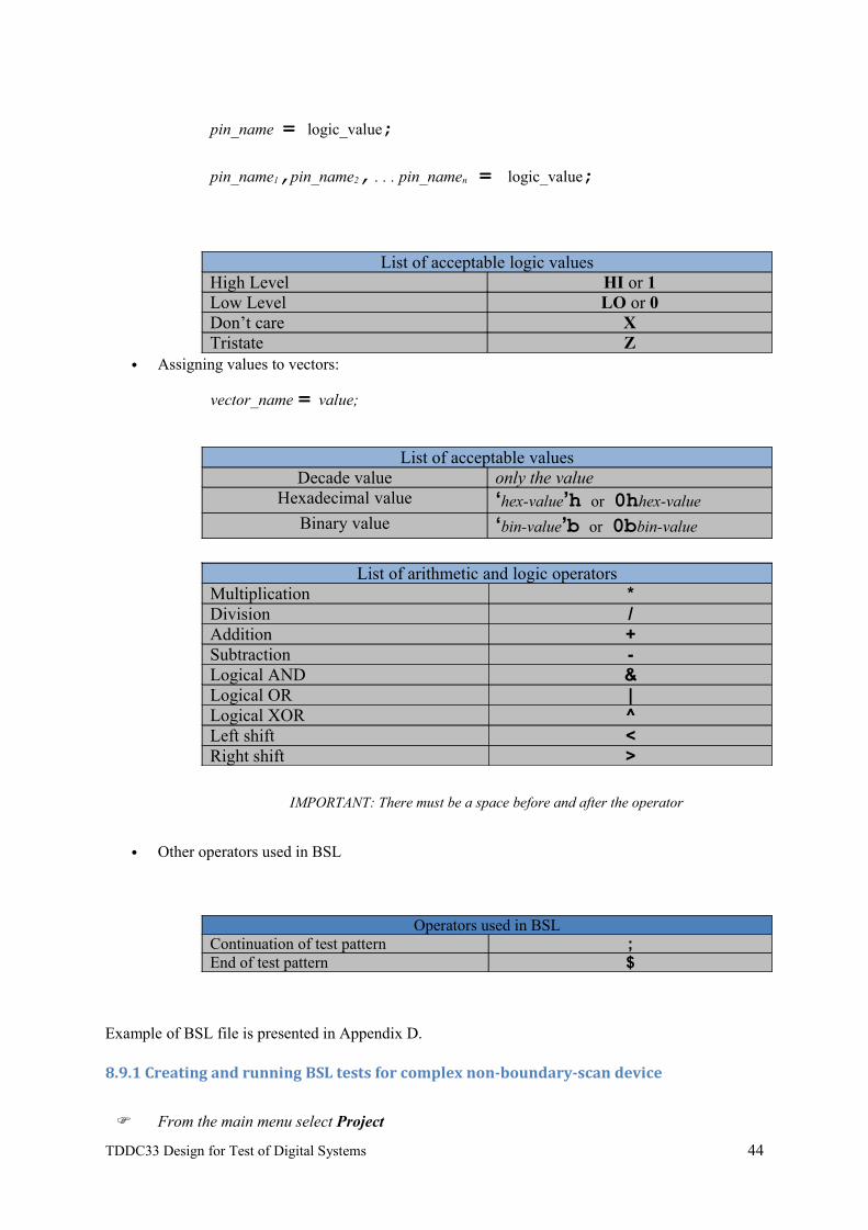
pin_name = logic_value;
pin_name1,pin_name2, . . . pin_namen = logic_value;
List of acceptable logic valuesHigh Level HI or 1Low Level LO or 0Don’t care XTristate Z
• Assigning values to vectors:
vector_name = value;
List of acceptable valuesDecade value only the value
Hexadecimal value ‘hex-value’h or 0hhex-value
Binary value ‘bin-value’b or 0bbin-value
List of arithmetic and logic operatorsMultiplication *Division /Addition +Subtraction -Logical AND &Logical OR |Logical XOR ^Left shift <Right shift >
IMPORTANT: There must be a space before and after the operator
• Other operators used in BSL
Operators used in BSLContinuation of test pattern ;End of test pattern $
Example of BSL file is presented in Appendix D.
8.9.1 Creating and running BSL tests for complex non-boundary-scan device
From the main menu select Project
TDDC33 Design for Test of Digital Systems 44
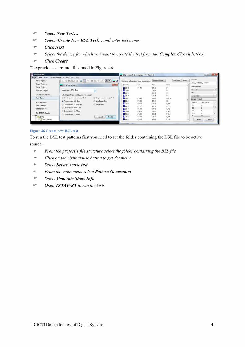
Select New Test…
Select Create New BSL Test… and enter test name
Click Next
Select the device for which you want to create the test from the Complex Circuit listbox.
Click Create
The previous steps are illustrated in Figure 46.
Figure 46 Create new BSL test
To run the BSL test patterns first you need to set the folder containing the BSL file to be active
source.
From the project’s file structure select the folder containing the BSL file
Click on the right mouse button to get the menu
Select Set as Active test
From the main menu select Pattern Generation
Select Generate Show Info
Open TSTAP-RT to run the tests
TDDC33 Design for Test of Digital Systems 45
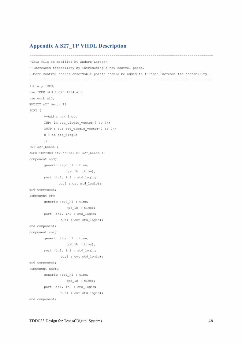
Appendix A S27_TP VHDL Description
----------------------------------------------------------------------------------------------
-This file is modified by Anders Larsson
--Increased testability by introducing a new control point.
--More control and/or observable points should be added to further increase the testability.
---------------------------------------------------------------------------------------------
library IEEE;
use IEEE.std_logic_1164.all;
use work.all;
ENTITY s27_bench IS
PORT (
--Add a new input
INP: in std_ulogic_vector(0 to 4);
OUTP : out std_ulogic_vector(0 to 0);
H : in std_ulogic
);
END s27_bench ;
ARCHITECTURE structural OF s27_bench IS
component andg
generic (tpd_hl : time;
tpd_lh : time);
port (in1, in2 : std_logic;
out1 : out std_logic);
end component;
component org
generic (tpd_hl : time;
tpd_lh : time);
port (in1, in2 : std_logic;
out1 : out std_logic);
end component;
component xorg
generic (tpd_hl : time;
tpd_lh : time);
port (in1, in2 : std_logic;
out1 : out std_logic);
end component;
component xnorg
generic (tpd_hl : time;
tpd_lh : time);
port (in1, in2 : std_logic;
out1 : out std_logic);
end component;
TDDC33 Design for Test of Digital Systems 46
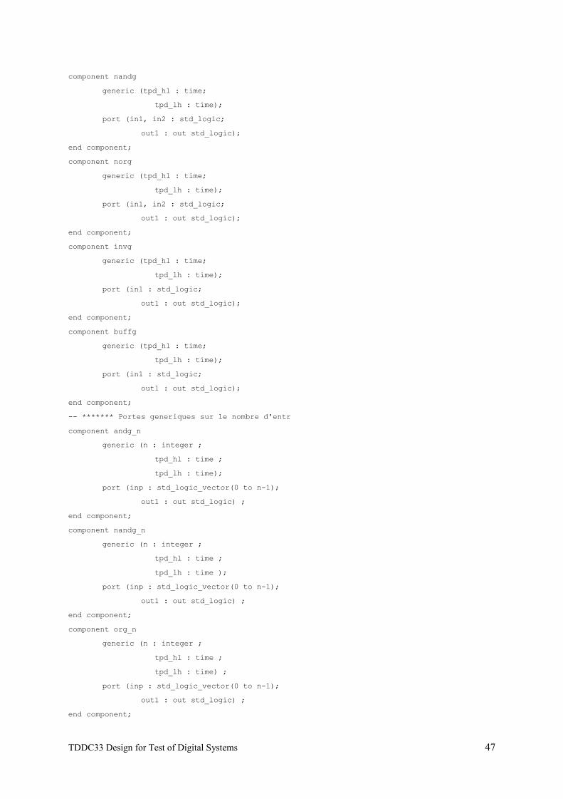
component nandg
generic (tpd_hl : time;
tpd_lh : time);
port (in1, in2 : std_logic;
out1 : out std_logic);
end component;
component norg
generic (tpd_hl : time;
tpd_lh : time);
port (in1, in2 : std_logic;
out1 : out std_logic);
end component;
component invg
generic (tpd_hl : time;
tpd_lh : time);
port (in1 : std_logic;
out1 : out std_logic);
end component;
component buffg
generic (tpd_hl : time;
tpd_lh : time);
port (in1 : std_logic;
out1 : out std_logic);
end component;
-- ******* Portes generiques sur le nombre d'entr
component andg_n
generic (n : integer ;
tpd_hl : time ;
tpd_lh : time);
port (inp : std_logic_vector(0 to n-1);
out1 : out std_logic) ;
end component;
component nandg_n
generic (n : integer ;
tpd_hl : time ;
tpd_lh : time );
port (inp : std_logic_vector(0 to n-1);
out1 : out std_logic) ;
end component;
component org_n
generic (n : integer ;
tpd_hl : time ;
tpd_lh : time) ;
port (inp : std_logic_vector(0 to n-1);
out1 : out std_logic) ;
end component;
TDDC33 Design for Test of Digital Systems 47
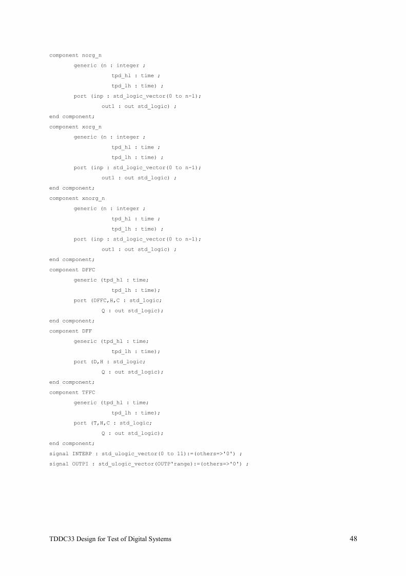
component norg_n
generic (n : integer ;
tpd_hl : time ;
tpd_lh : time) ;
port (inp : std_logic_vector(0 to n-1);
out1 : out std_logic) ;
end component;
component xorg_n
generic (n : integer ;
tpd_hl : time ;
tpd_lh : time) ;
port (inp : std_logic_vector(0 to n-1);
out1 : out std_logic) ;
end component;
component xnorg_n
generic (n : integer ;
tpd_hl : time ;
tpd_lh : time) ;
port (inp : std_logic_vector(0 to n-1);
out1 : out std_logic) ;
end component;
component DFFC
generic (tpd_hl : time;
tpd_lh : time);
port (DFFC,H,C : std_logic;
Q : out std_logic);
end component;
component DFF
generic (tpd_hl : time;
tpd_lh : time);
port (D,H : std_logic;
Q : out std_logic);
end component;
component TFFC
generic (tpd_hl : time;
tpd_lh : time);
port (T,H,C : std_logic;
Q : out std_logic);
end component;
signal INTERP : std_ulogic_vector(0 to 11):=(others=>'0') ;
signal OUTPI : std_ulogic_vector(OUTP'range):=(others=>'0') ;
TDDC33 Design for Test of Digital Systems 48
BEGIN
DFF0 : DFF generic map (1 ns,1 ns)
port map (
D => INTERP(1),
H => H,
Q => INTERP(0));
DFF1 : DFF generic map (1 ns,1 ns)
port map (
D => INTERP(3),
H => H,
Q => INTERP(2));
DFF2 : DFF generic map (1 ns,1 ns)
port map (
D => INTERP(5),
H => H,
Q => INTERP(4));
INV0 : INVG generic map (1 ns,1 ns)
port map (
in1 => INP(0),
out1 => INTERP(6));
INV1 : INVG generic map (1 ns,1 ns)
port map (
in1 => INTERP(3),
out1 => OUTPI(0));
AND0 : ANDG_N generic map (2,1 ns,1 ns)
port map (
inp(0) => INTERP(6),
inp(1) => INTERP(2),
out1 => INTERP(7));
OR0 : ORG_N generic map (2,1 ns,1 ns)
port map (
inp(0) => INTERP(9),
inp(1) => INTERP(7),
out1 => INTERP(8));
OR1 : ORG_N generic map (2,1 ns,1 ns)
port map (
inp(0) => INP(3),
inp(1) => INTERP(7),
out1 => INTERP(10));
NAND0 : NANDG_N generic map (2,1 ns,1 ns)
port map (
inp(0) => INTERP(10),
inp(1) => INTERP(8),
out1 => INTERP(11));
TDDC33 Design for Test of Digital Systems 49
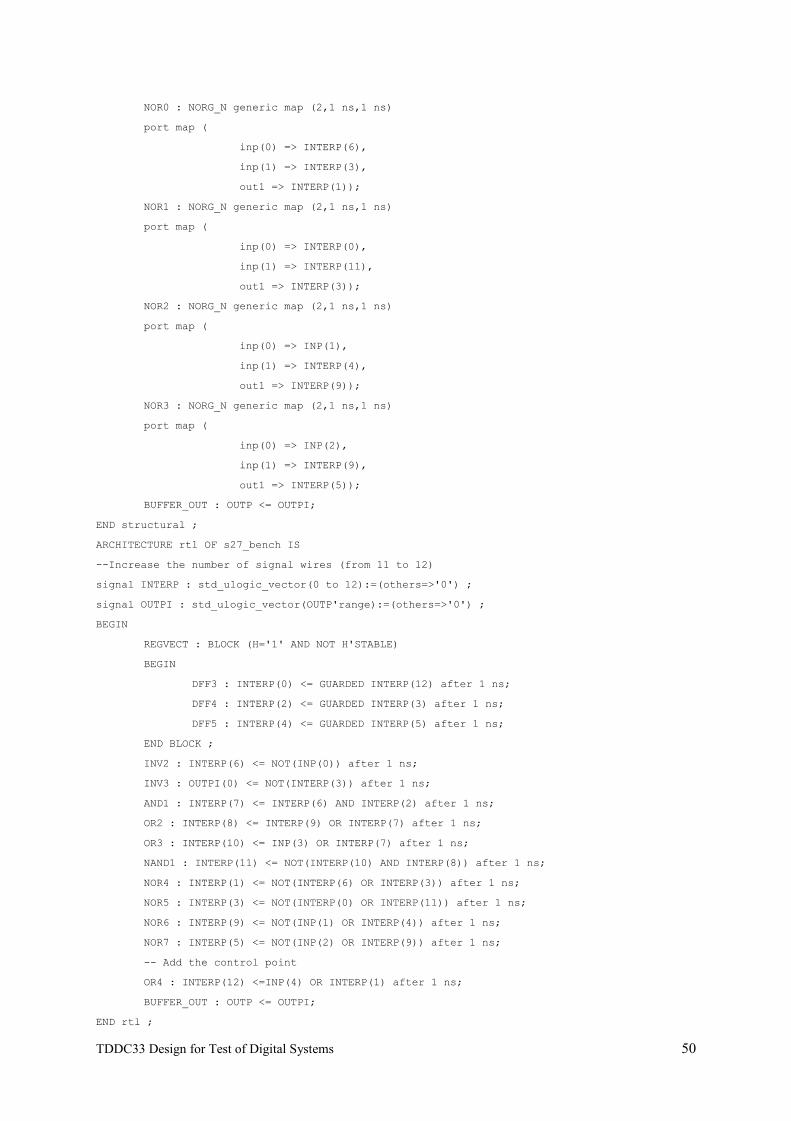
NOR0 : NORG_N generic map (2,1 ns,1 ns)
port map (
inp(0) => INTERP(6),
inp(1) => INTERP(3),
out1 => INTERP(1));
NOR1 : NORG_N generic map (2,1 ns,1 ns)
port map (
inp(0) => INTERP(0),
inp(1) => INTERP(11),
out1 => INTERP(3));
NOR2 : NORG_N generic map (2,1 ns,1 ns)
port map (
inp(0) => INP(1),
inp(1) => INTERP(4),
out1 => INTERP(9));
NOR3 : NORG_N generic map (2,1 ns,1 ns)
port map (
inp(0) => INP(2),
inp(1) => INTERP(9),
out1 => INTERP(5));
BUFFER_OUT : OUTP <= OUTPI;
END structural ;
ARCHITECTURE rtl OF s27_bench IS
--Increase the number of signal wires (from 11 to 12)
signal INTERP : std_ulogic_vector(0 to 12):=(others=>'0') ;
signal OUTPI : std_ulogic_vector(OUTP'range):=(others=>'0') ;
BEGIN
REGVECT : BLOCK (H='1' AND NOT H'STABLE)
BEGIN
DFF3 : INTERP(0) <= GUARDED INTERP(12) after 1 ns;
DFF4 : INTERP(2) <= GUARDED INTERP(3) after 1 ns;
DFF5 : INTERP(4) <= GUARDED INTERP(5) after 1 ns;
END BLOCK ;
INV2 : INTERP(6) <= NOT(INP(0)) after 1 ns;
INV3 : OUTPI(0) <= NOT(INTERP(3)) after 1 ns;
AND1 : INTERP(7) <= INTERP(6) AND INTERP(2) after 1 ns;
OR2 : INTERP(8) <= INTERP(9) OR INTERP(7) after 1 ns;
OR3 : INTERP(10) <= INP(3) OR INTERP(7) after 1 ns;
NAND1 : INTERP(11) <= NOT(INTERP(10) AND INTERP(8)) after 1 ns;
NOR4 : INTERP(1) <= NOT(INTERP(6) OR INTERP(3)) after 1 ns;
NOR5 : INTERP(3) <= NOT(INTERP(0) OR INTERP(11)) after 1 ns;
NOR6 : INTERP(9) <= NOT(INP(1) OR INTERP(4)) after 1 ns;
NOR7 : INTERP(5) <= NOT(INP(2) OR INTERP(9)) after 1 ns;
-- Add the control point
OR4 : INTERP(12) <=INP(4) OR INTERP(1) after 1 ns;
BUFFER_OUT : OUTP <= OUTPI;
END rtl ;
TDDC33 Design for Test of Digital Systems 50
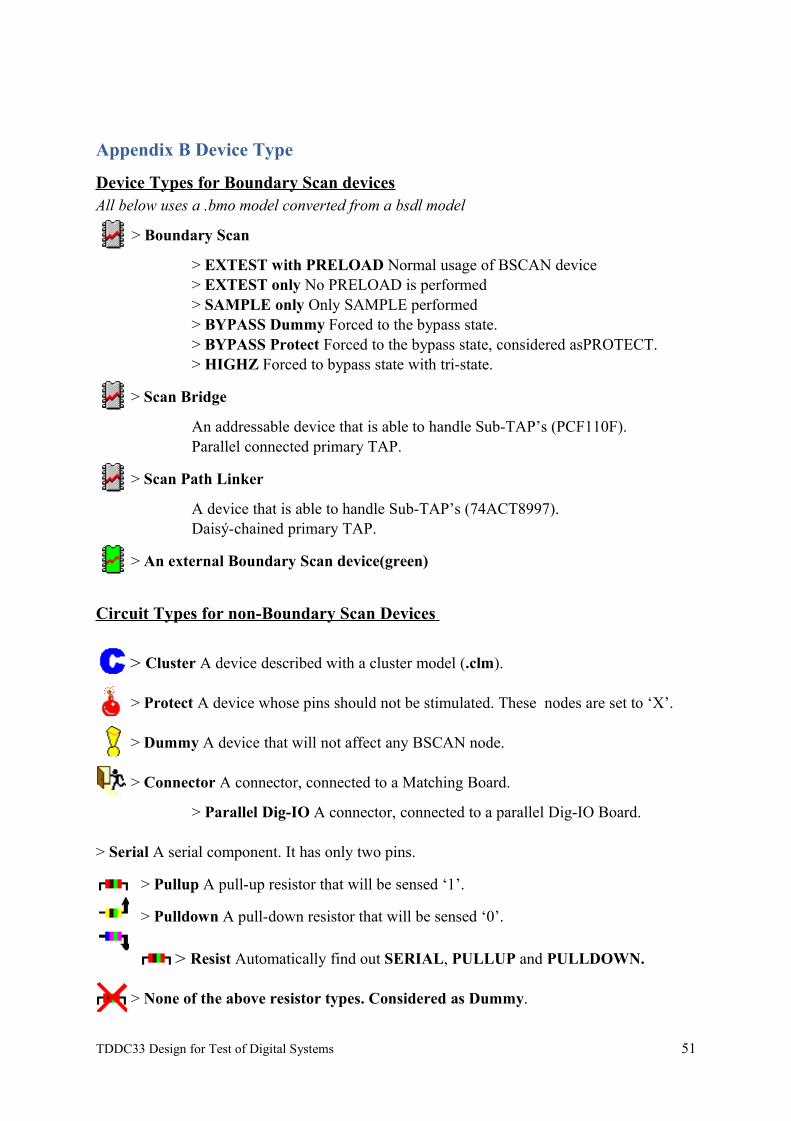
Appendix B Device Type
Device Types for Boundary Scan devicesAll below uses a .bmo model converted from a bsdl model
> Boundary Scan
> EXTEST with PRELOAD Normal usage of BSCAN device> EXTEST only No PRELOAD is performed> SAMPLE only Only SAMPLE performed> BYPASS Dummy Forced to the bypass state.> BYPASS Protect Forced to the bypass state, considered asPROTECT.> HIGHZ Forced to bypass state with tri-state.
> Scan Bridge
An addressable device that is able to handle Sub-TAP’s (PCF110F).Parallel connected primary TAP.
> Scan Path Linker
A device that is able to handle Sub-TAP’s (74ACT8997).Daisý-chained primary TAP.
> An external Boundary Scan device(green)
Circuit Types for non-Boundary Scan Devices
> Cluster A device described with a cluster model (.clm).
> Protect A device whose pins should not be stimulated. These nodes are set to ‘X’.
> Dummy A device that will not affect any BSCAN node.
> Connector A connector, connected to a Matching Board.
> Parallel Dig-IO A connector, connected to a parallel Dig-IO Board.
> Serial A serial component. It has only two pins.
> Pullup A pull-up resistor that will be sensed ‘1’.
> Pulldown A pull-down resistor that will be sensed ‘0’.
> Resist Automatically find out SERIAL, PULLUP and PULLDOWN.
> None of the above resistor types. Considered as Dummy.
TDDC33 Design for Test of Digital Systems 51
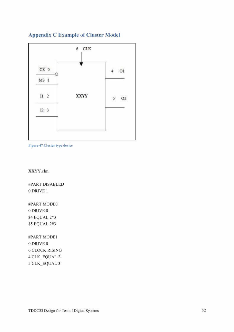
Appendix C Example of Cluster Model
Figure 47 Cluster type device
XXYY.clm
#PART DISABLED
0 DRIVE 1
#PART MODE0
0 DRIVE 0
$4 EQUAL 2*3
$5 EQUAL 2#3
#PART MODE1
0 DRIVE 0
6 CLOCK RISING
4 CLK_EQUAL 2
5 CLK_EQUAL 3
TDDC33 Design for Test of Digital Systems 52
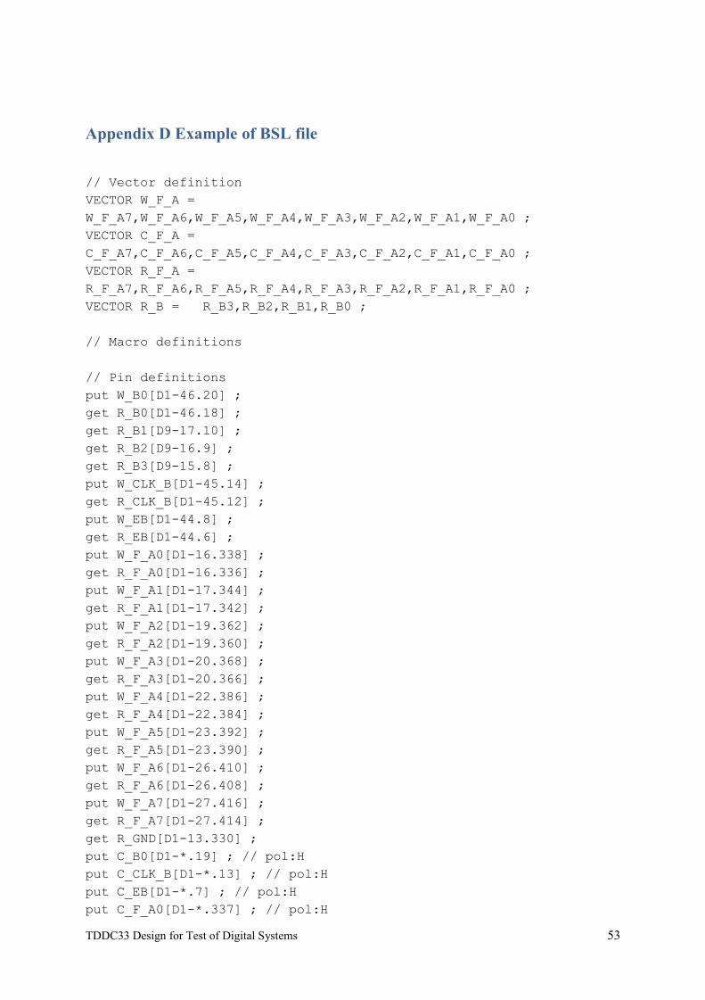
Appendix D Example of BSL file
// Vector definitionVECTOR W_F_A = W_F_A7,W_F_A6,W_F_A5,W_F_A4,W_F_A3,W_F_A2,W_F_A1,W_F_A0 ;VECTOR C_F_A = C_F_A7,C_F_A6,C_F_A5,C_F_A4,C_F_A3,C_F_A2,C_F_A1,C_F_A0 ;VECTOR R_F_A = R_F_A7,R_F_A6,R_F_A5,R_F_A4,R_F_A3,R_F_A2,R_F_A1,R_F_A0 ;VECTOR R_B = R_B3,R_B2,R_B1,R_B0 ;
// Macro definitions
// Pin definitionsput W_B0[D1-46.20] ;get R_B0[D1-46.18] ;get R_B1[D9-17.10] ;get R_B2[D9-16.9] ;get R_B3[D9-15.8] ;put W_CLK_B[D1-45.14] ;get R_CLK_B[D1-45.12] ;put W_EB[D1-44.8] ;get R_EB[D1-44.6] ;put W_F_A0[D1-16.338] ;get R_F_A0[D1-16.336] ;put W_F_A1[D1-17.344] ;get R_F_A1[D1-17.342] ;put W_F_A2[D1-19.362] ;get R_F_A2[D1-19.360] ;put W_F_A3[D1-20.368] ;get R_F_A3[D1-20.366] ;put W_F_A4[D1-22.386] ;get R_F_A4[D1-22.384] ;put W_F_A5[D1-23.392] ;get R_F_A5[D1-23.390] ;put W_F_A6[D1-26.410] ;get R_F_A6[D1-26.408] ;put W_F_A7[D1-27.416] ;get R_F_A7[D1-27.414] ;get R_GND[D1-13.330] ;put C_B0[D1-*.19] ; // pol:Hput C_CLK_B[D1-*.13] ; // pol:Hput C_EB[D1-*.7] ; // pol:Hput C_F_A0[D1-*.337] ; // pol:H
TDDC33 Design for Test of Digital Systems 53
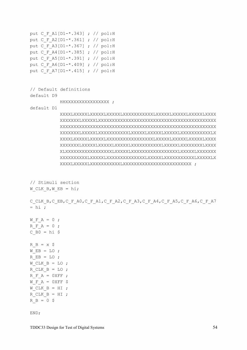
put C_F_A1[D1-*.343] ; // pol:Hput C_F_A2[D1-*.361] ; // pol:Hput C_F_A3[D1-*.367] ; // pol:Hput C_F_A4[D1-*.385] ; // pol:Hput C_F_A5[D1-*.391] ; // pol:Hput C_F_A6[D1-*.409] ; // pol:Hput C_F_A7[D1-*.415] ; // pol:H
// Default definitionsdefault D9
HHXXXXXXXXXXXXXXXX ;default D1
XXXXLXXXXXLXXXXXLXXXXXLXXXXXXXXXXXLXXXXXLXXXXXLXXXXXLXXXXXXXXXXXLXXXXXLXXXXXXXXXXXXXXXXXXXXXXXXXXXXXXXXXXXXXXXXXXXXXXXXXXXXXXXXXXXXXXXXXXXXXXXXXXXXXXXXXXXXXXXXXXXXXXXXXXXXXXXXXXXLXXXXXLXXXXXXXXXXXLXXXXXLXXXXXLXXXXXLXXXXXXXXXXXLXXXXXLXXXXXLXXXXXLXXXXXXXXXXXXXXXXXLXXXXXLXXXXXLXXXXXLXXXXXXXXXXXLXXXXXLXXXXXLXXXXXLXXXXXXXXXXXLXXXXXLXXXXXXXXLXXXXXLXXXXXXXXXXXXXXXXXLXXXXXLXXXXXXXXXXXXXXXXXLXXXXXLXXXXXXXXXXXXXXXXXLXXXXXLXXXXXXXXXXXXXXLXXXXXLXXXXXXXXXXXLXXXXXLXXXXXLXXXXXLXXXXXXXXXXXLXXXXXXXXXXXXXXXXXXXXXXXXX ;
// Stimuli sectionW_CLK_B,W_EB = hi;
C_CLK_B,C_EB,C_F_A0,C_F_A1,C_F_A2,C_F_A3,C_F_A4,C_F_A5,C_F_A6,C_F_A7 = hi ;
W_F_A = 0 ;R_F_A = 0 ;C_B0 = hi $
R_B = x $W_EB = LO ;R_EB = LO ;W_CLK_B = LO ;R_CLK_B = LO ;R_F_A = 0XFF ;W_F_A = 0XFF $W_CLK_B = HI ;R_CLK_B = HI ;R_B = 0 $
END;
TDDC33 Design for Test of Digital Systems 54

References
[1] http://asic.austriamicrosystems.com/databooks/c35/databook_c35_33/, April 2006.
TDDC33 Design for Test of Digital Systems 55