Embed Size (px)
Citation preview
AD-A272 848|l Ill) II I)I IDIDIIAIiN,
Final ReportContract No.: ONR N00014-88-K-0317
(ONR N00014-92-J-1868)
Properties of E-beam Interactive Oxide Filmsfor Nanometer Scale Structures
by
r --" ECTE R. C. Buchanan*
. 1 8 1993 " J. L. Hollenbeck' " AJ. Kim*
October 1993
Department of Materials Science and Engineering
Ceramic Division
University of Illinois at Urbana-Champaign105 S (;oodwin Ave.
Urbana, IL -61801
Soi pubirjj eie.e.d zeiu im
Thi,; research was supported by DARPA underOffice of Naval Research Sponsorship
Production in whole or in part is permitted for
any purpose of the United States Government
*Current Address Univ of Cincinnati, 499 Rhodes Hall, Cincinnati, OH 45221
9. 11 1? 013
S S 0 0 S 0b 0 0
'EdL RITY CLASSIFICATION OF THIlS PAGE
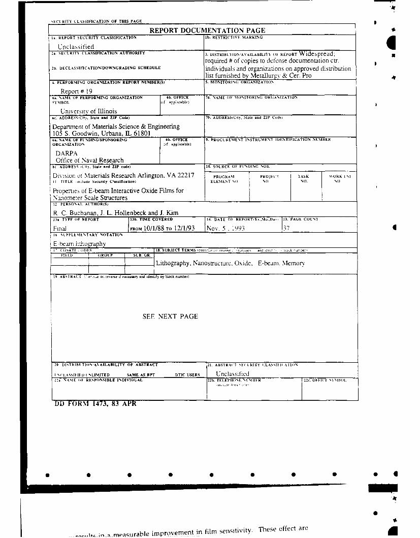
REPORT DOCUMENTATION PAGE1,, REPORT SECURITY CLASSIFICATION Ilb. RESTRICTIVE MARKING
Unclassified__________________________2.. SECURIT'i CLASSIFICATION AUTHORITY 3. DISTRIBCTIDN'A%'AILABILITY' (I REPORT Widespreadý X
required # of copies to defense documentation ctr.2b. D)ECLASSIFICATION/IDOW'NGRADING SCHEDULE individuals and organizations on approved distribution
______________________________________list furnished by Metallurgy & Cer. Pro4. PERFORMING ORGANIZATION REPORT NUMBER(S) 5. MONITORING ORGANIZATION
Report # 19______ ________________ _____
6a. NAME OF PERFORMING ORGANIZATION 6 b. OFFICE 7a. NAME OF %IONIlIORIG ORGANIZATIONS) MBOL (if applicable)
Universitv of Illinoisbc. ADDRESSiCIt), State and ZIP Code) 7b. ADURESSýCuly, State and ZIP Code)
Departent of Materials Science & Engineering105 S. Goodwin, Urbana, IL 61801 ______ _____________________
6a. 'NAME OF FUNDL',GISPONSORING 6b. OFFICE 9. PROCU.REMIENT INSTRUMENT IDENTIFICATION NUMBERORGANIZATION (if applicable)
DARPAOffice of Naval Research _______________________________
8c ADDRESS CI.State and ZIP code) 10. SOURCE OF FUNDING NOS.
Division ot Mlaterials Research Arlington, VA 22217 PROGRAM PROliX) T ASK NkORK L N1
11TITLE include Security Clasalflcation) ELEMENT NO. NO. NO.N)
PropertieN, of E-beam Interactive Oxide Films forNanometer Scale Structures ________________________
1,PE RSON AL AU~THOR(S)
R. C. Buchanan, J. L. Hollenbeck and J. Kiml3a. TYPE OF REPORT ib. ThIME COVERED 114., DATE OF REPORTiVr.,M...D-' 115. PAGE COU~l
Final 71FROM 10/1/88 TO 1.2/1/93 N ov. 5 ,1991 37i16.1 PPLLEMF-NTAkY NOTATION
E-beam IiuhographyI-) OSATI :liE)S Iis. SUBJECT TERMS =Mn "cIen,'acd. .- I ,o n-nb''
FIELD G;ROIP I SUB. GR..I
AB4RCTLithography, Nanostructure. Oxide, E-beami. %lemory
19 ABnTRACT on r~enee J neceasary and Identify oy block nomber)
SEF NEXT PAGE
DD FORM 1473, 83 APR
mgo,'itrahib jiprovement in film sensitivity. These effect are
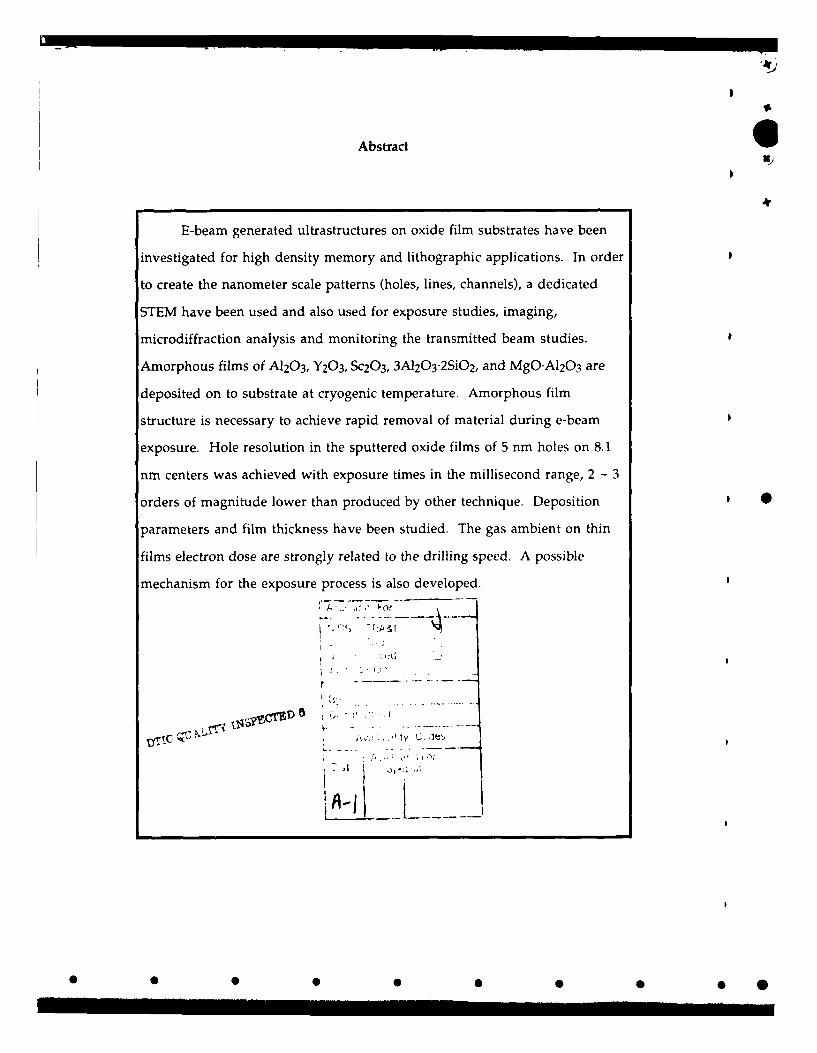
Abstract 6X)
E-beam generated ultrastructures on oxide film substrates have been
investigated for high density memory and lithographic applications. In order
to create the nanometer scale patterns (holes, lines, channels), a dedicated
STEM have been used and also used for exposure studies, imaging,
microdiffraction analysis and monitoring the transmitted beam studies.
Amorphous films of A120 3, Y203, Sc203, 3A12032SiO 2, and MgO'A1203 are
deposited on to substrate at cryogenic temperature. Amorphous film
structure is necessary to achieve rapid removal of material during e-beam
exposure. Hole resolution in the sputtered oxide films of 5 nm holes on 8.1
nm centers was achieved with exposure times in the millisecond range, 2 - 3
orders of magnitude lower than produced by other technique. Deposition '
parameters and film thickness have been studied. The gas ambient on thin
films electron dose are strongly related to the drilling speed. A possible
mechanism for the exposure process is also developed.
',' I- . J , -.O
S ..... . ......• • 0. .... .........
V!-"IC] o*A-
Table of ContentsI)
Page
L. Introduction I
IL Experimental Procedure 3
M. Results and Discussion 4
IV. Conclusions 13
V. Acknowledgements 14
VI. References 15
VII. List of Figures 17
I 0
S S S 0 0 0 0
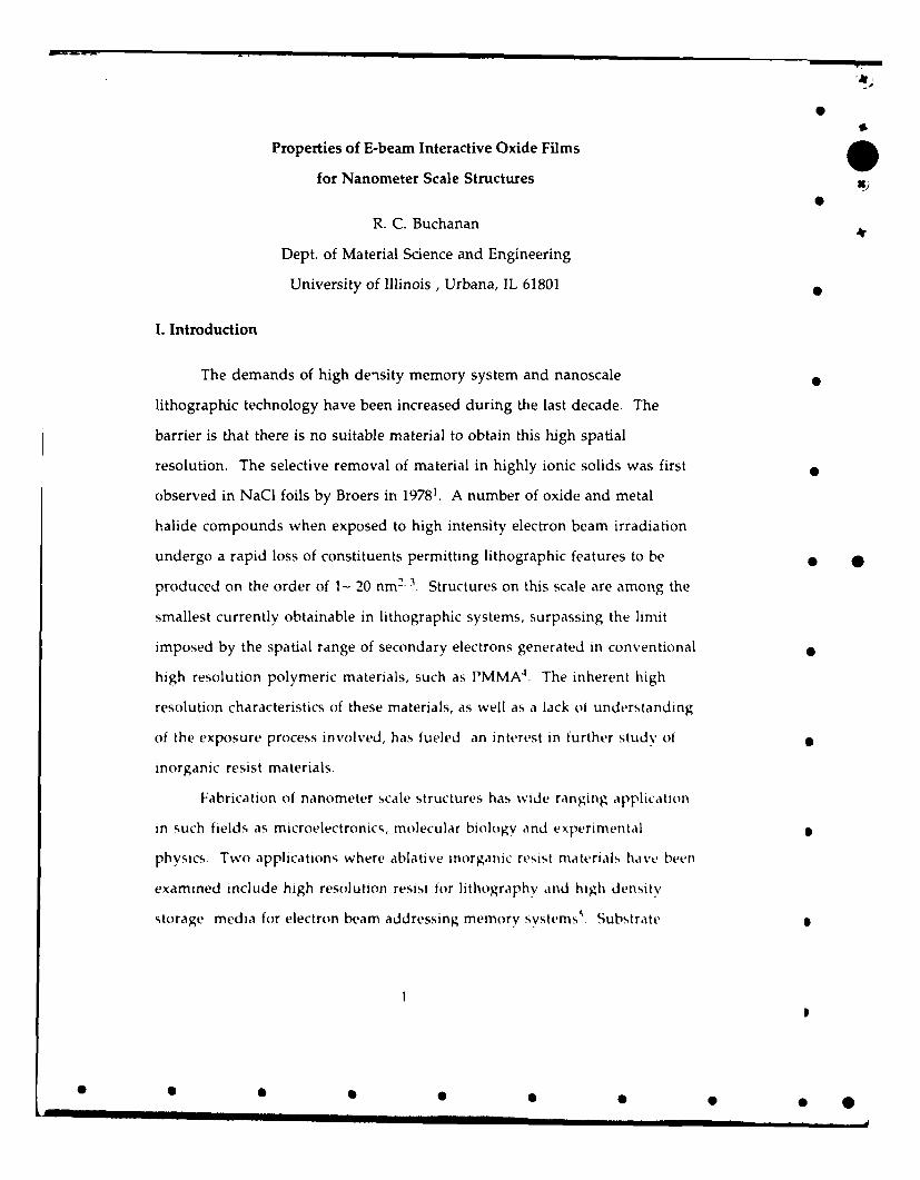
Properties of E-beam Interactive Oxide Films
for Nanometer Scale Structures X)
R. C. Buchanan 4
Dept. of Material Science and Engineering
University of Illinois , Urbana, IL 61801
I. Introduction
The demands of high density memory system and nanoscale
lithographic technology have been increased during the last decade. The
barrier is that there is no suitable material to obtain this high spatial
resolution. The selective removal of material in highly ionic solids was first
observed in NaCl foils by Broers in 1978'. A number of oxide and metal
halide compounds when exposed to high intensity electron beam irradiation
undergo a rapid loss of constituents permitting lithographic features to be • *produced on the order of 1- 20 nm 2 3. Structures on this scale are among the
smallest currently obtainable in lithographic systems, surpassing the limit
imposed by the spatial range of secondary electrons generated in conventional
high resolution polymeric materials, such as PMMA 4. The inherent high
resolution characteristics of these materials, as well as a lack of understanding
of the exposure process involved, has fueled an interest in further study of
inorganic resist materials.
Fabrication of nanometer scale structures has wide ranging application
in such fields as microelectronics, molecular biology and experimental
physics Two applications where ablative inorganic resist materials have been
examined include high resolution resist for lithography and high density
storage media for electron beam addressing memory svstems'. Substrate
, • •• • • •• •
S 50SS
IS
characteristics desirable in the above applications, in addition to nanometer
scale resolution, include low dosage requirements for exposure, high material
removal rates, high contrast, good physical and chemical durability and good 0
thermal conductivity.
To date the majority of studies reported on high resolution inorganic
resists concentrated on metal halides. In these materials, material loss
strongly depends on composition. In addition, the lithographic characteristics
of oxide materials have been observed by Hollenbeck and Buchanan 6. 7 to
depend on the method of film preparation and on the resulting 0
microstructura' characteristics. The latter studies have shown that proper
control of film deposition should produce improvements in resist properties,
particularly exposure requirements.
It is the purpose of this research to develop new oxide resist materials
capable of nanoscale resolution and to determine the interrelationships
between the various parameters of a lithographic system. The results show
that film characters are sensitive to the exposure of rf sputtered films
included amorphous film structure , inert g,v concentration, ionic character,
heat of formation, and film thickness. The dose rate and energy of the
incident beam were also found to influence the does requirement for
exposure The most sensitive films were found to be A1201, Y203, Sc201,
3A1201 25102, and MgO-AI201 which required an exposure dose of
approXimately 5. 10" C/cm 2 The ultimate resolution in amorphous Al201
films consisted of 5.0 nm holes on S.9 nm centers. The exposure process was
modeled as a sequence of events beginning with desorption of surface oxygen
and generation of bulk defects, as followed by extensive surface desorption,
diffusion of bulk defects and rapid expulsion of components remaining in the
irradiated volume.
2S
S 0 S S S S 5 5 0
II. Experimental Procedure
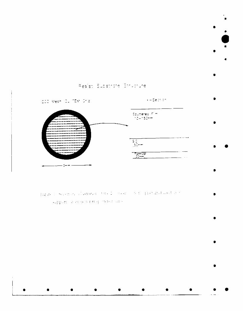
The oxide films were deposited by rf sputtering from dense
polycrystalline oxide tagets directly onto formvar coated 200 mesh grids
stabilized with SiO. The resulting resist/substrate arrangement is shown in
figure 1. The formvar and SiO coatings are amorphous and show no
deterioration under exposure conditions. Sputtering parameters were chosen
to allow the fabrication of both polycrystalline and amorphous films from 15
- 150 nm in thickness. To promote the formation of amorphous films, the
substrate temperature was controlled at 77 K through the use of a liquid
nitrogen cold stage.
Electron beam exposure of the thin oxide films was carried out using a
modified V. G. Microscope HB-5 STEM, capable of producing a 100 keV beam
of electrons with a dose rate of Nx10 5 A/cm 2 and a final spot diameter less
than 1 nm. Generation of lithographic patterns is being carried out through
computer control of the beam deflection and beam blanking systems in the
microscope.
Structural and chemical chraterization was primary done by a Philips
EM400T equipped with EDS and RBS. The RBS analysis was carried out using
incident 1 MeV He+ and was performed on samples deposited on polished Si
wafers. The microdiffraction capability of the V. G. HB-5 allowed electron
diffraction analysis to be performed on individual crystallites as small as the
beam spot size(l nm) when operating the microscope in spot mode. This
permitted analysis of local structural and crystallographic changes
accompanying the formation of nanometer scale features. Digital image
enhancement features of the system were used in anlyzing diffraction data.
3
S
III. Results and Discussion NJ
4"The two most important deposition parameters found to influence the
microstructure of rf sputtered oxide films were substrate temperature and rf
power. Deposition conditions necessary to promote the formation of
uniform amorphous films were also found to be strongly dependent on the
material itself. Using a substrate temperature of 77 K amorphous film
structure was produced in seven of the eight oxides studied. The deposition
of films at cryogenic temperature limited diffusion of adatoms on growing
films and resulted almost exclusively in amorphous film structures. Limited
sputtering power minimized local heating of the film surface during
deposition. To avoid local surface heating in films, powers were limited to
less than 50 Watts and a 10 min cooling period for every 30 min of deposition
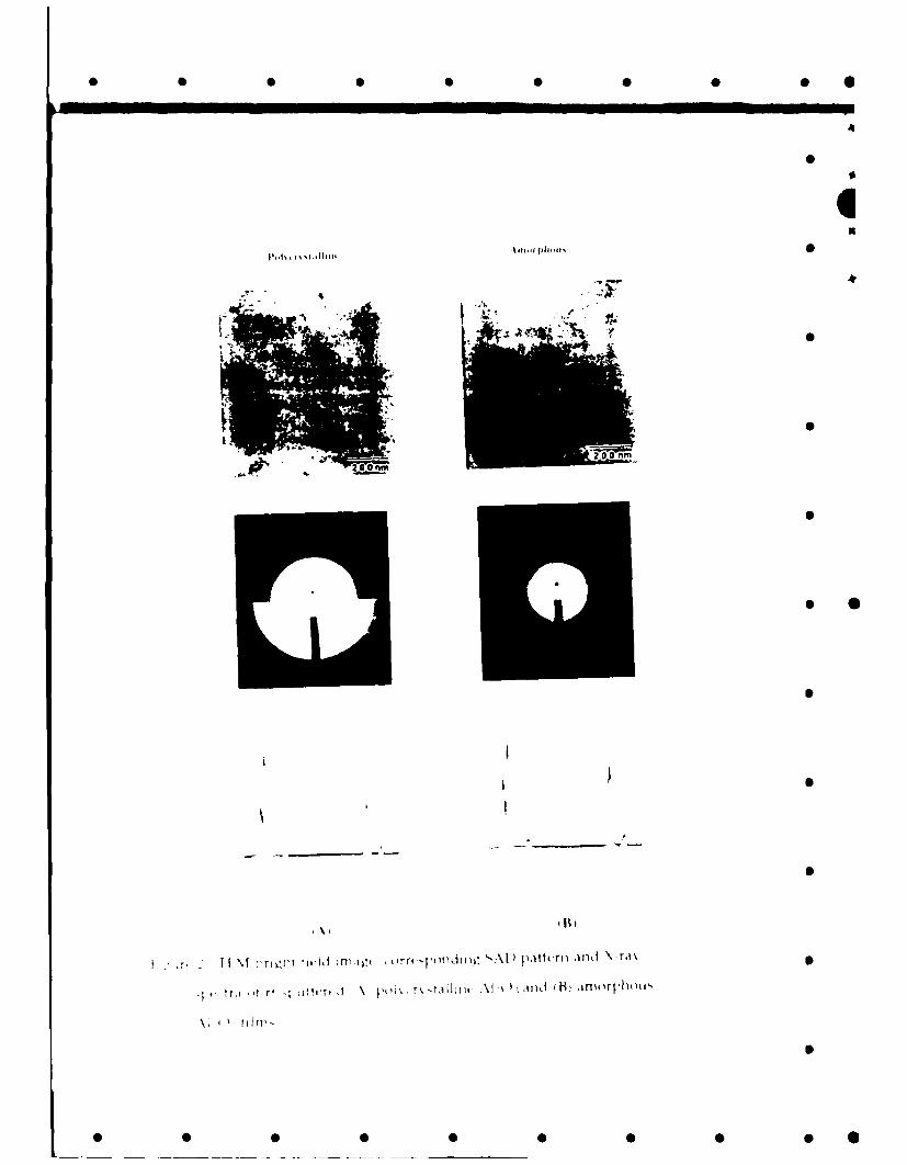
time. Bright field TEM images of polycrystalline and amorphous A120 3 films
along with their corresponding SAD patterns and X-ray spectra are shown in
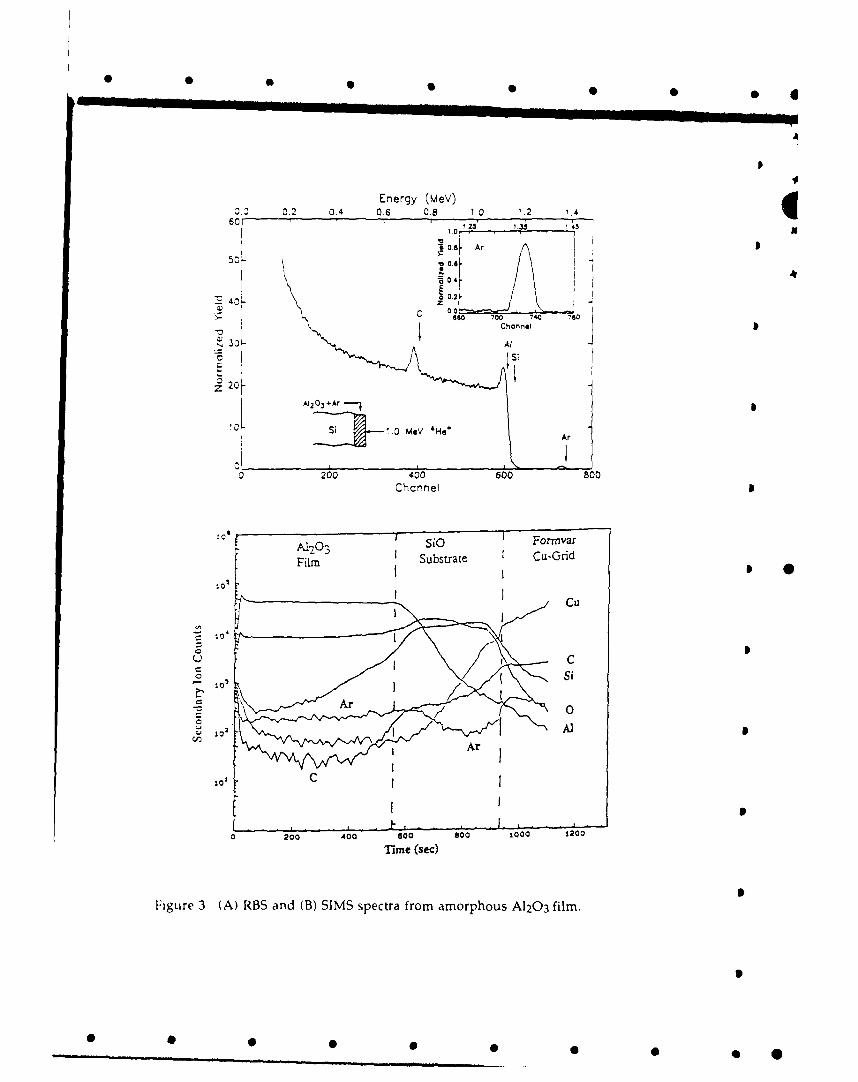
figure 2. RBS data from a series of amorphous A120 3 films was used to
establish quantitative standards and to confirm the Ar concentrations
determined by X-ray analysis. Ar concentration measured by X-ray and RBS
analysis in a series of three films were found to agree with ±0.1% atomic %.
SIMS spectra used to determine the Ar concentration changes were checked.
The Ar concentration was found to not fluctuate in whole films. These data
are shown in figure 3. The amorphous films showed good uniformity, good
density, very little contrast and a characteristic diffuse diffraction pattern. X-
ray spectra shows that the relative intensity of Ar peaks is different between
polycrystalline and amorphous films. The Ar concentration was found to
range from approximately 1.7 - 3.1 at% in amorphous films depend on
4
deposition condition. The summary of rf sputtered films structures is shown
in table 1. W
The initial response of rf sputtered oxide films under E-beam dose rate 4.
of approximately 1x10 5 A/cm 2 . Polycrystalline oxide films showed no mass
loss or lithographic response under extended periods (>10 s) of irradiation.
Amorphous films were found to exhibit lithographic characteristics with the
dose required for exposure varying from approximately 1x10 5 A/cm 2 (-50 ms)
in the most sensitive materials. The initial response of e-beam dose is
summarized in table 2. It becomes clear from the data in table 2 that removal
of material under exposure conditions is strongly dependent on both film
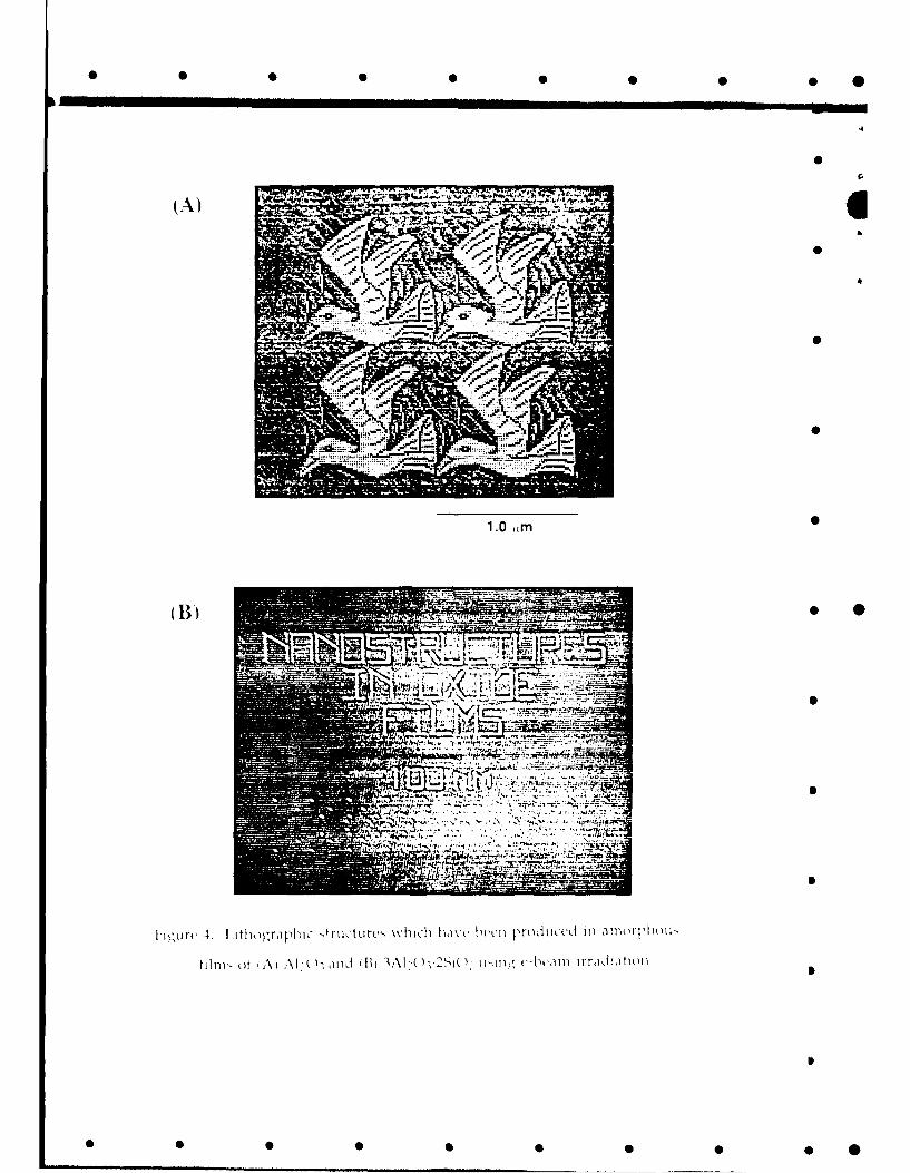
structure and composition. Examples of lithographic structures which can be
produced in the six oxides showing nanometer scale lithographic
characteristics are shown in figure 4 (A) and (B). These structures include
both holes, which are actually columns in 3-dimensions, and lines, which are
troughs in 3-dimension.
The dose requirement of rf sputtered films of A1203, Y20 3, Sc203,
3A1203.2SiO 2, and MgO-A1203 have also been found to show a response
which is two or three orders of magnitude more sensitive than oxides
produced by such techniques as anodization 5 , collection of smoke particles' or
crushing of powders9 . Although films prepared by other techniques have not
been well characterized, one obvious chemical difference in the rf sputtered
films is the presence of inert gas. The large increase in sensitivity observed in
rf sputtered films indicates that inert gas incorporated into the film structure
may, at least in part, be responsible for improved sensitivity.
A summary of selected material properties of the single metal oxides
examined is given in table 3. Material properties which were found to
correlate well with the exposure response of amorphous oxide films were the
5 S
bonding character, heat of formation and melting point. A rapid response
was found to occur in materials with high ionic character, high heats of X,
formation and high melting points. The highly ionic materials with high
bonding strength are required to produce films with sufficient sensitivity to
make them viable resists.
The process of material removal which occurs during the exposure of a
single hole in amorphous A120 3 was studied using multiple dose / multiple
spacing test pattern and monitoring of transmitted beam signal. Figure 5
shows a STEM bright field image of a test pattern generated using four 0
different total doses, or exposure times and four different hole spacings. Also
shown in figure 5 is the hole diameter produced as a function of exposure
time and a trace of the transmitted beam signal for the consecutive holes in 0
amorphous A120 3. From the bright field image and a plot of hole size vs.
total dose it was found that small incomplete holes were produced during
initial exposure and that these holes continued to increase in diameter upon
further exposure. This increase in hole size continued until a diameter of
approximately 10.6 nm was reached.
Direct evidence that atomic displacement occurs over the range of
many atomic spacings during exposure was observed both in the redeposition
of material into fully developed closely spaced hole and line structures, and
in the formation of small crystallites at the edges of newly formed structures.
Figure 6 shows two conditions under which material was found to be
redeposited in previously exposed areas: (A) when the e-beam was scanned
over relatively small area and (B) when line or hole patterns intersect or are
spaced very close together. (A) shows a pattern produced in amorphous
A120 3 in which a portion of the pattern has been observed at higher
magnification under normal bright field scanning conditions. This area of
6
the pattern shows that the diameter of existing holes was reduced from
redepostion of material into them and the entire area appears brighter due to aS
loss of material in the previously unexposed regions between holes. In (B)
the vertical series of lines initially produced in amorphous 3A12Oy2SiO2
were found to be refilled by subsequently exposed horizontal lines. Refilled
regions are most easily seen in segments of the vertical lines between the
horizontal lines.
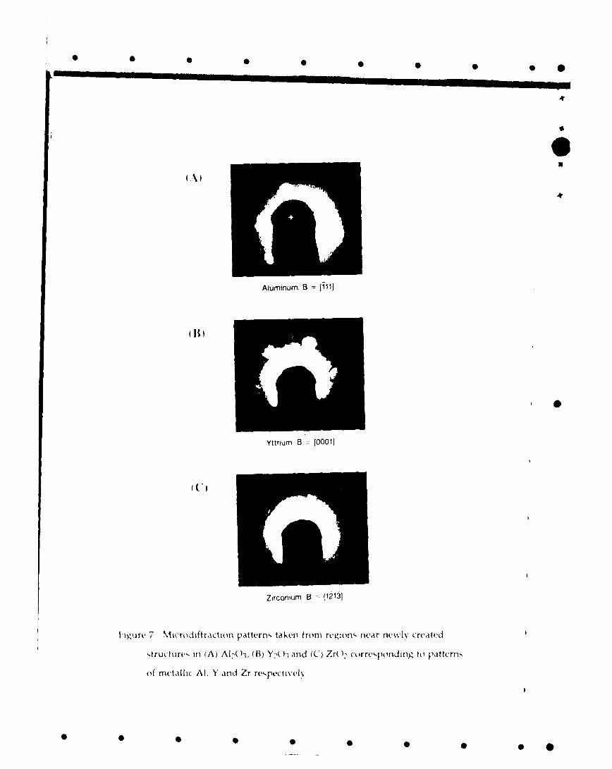
The formation of small crystallites was observed in STEM bright field
images after the exposure of many different patterns. Microdiffraction
patterns produced from similar crystallites, formed both near newly exposed
patterns and at hole and line edges, are shown in figure 7. The three
microdiffraction patterns were taken from amorphous films of A12 0 3 , Y2 0 3
and ZrO2 and were found to correspond to Al, Y, Zr patterns respectively.
The metal constituents in the irradiated volume of the film thus appear to be
spatially separated from the lattice oxygens during exposure and were reduced
to the metallic state.
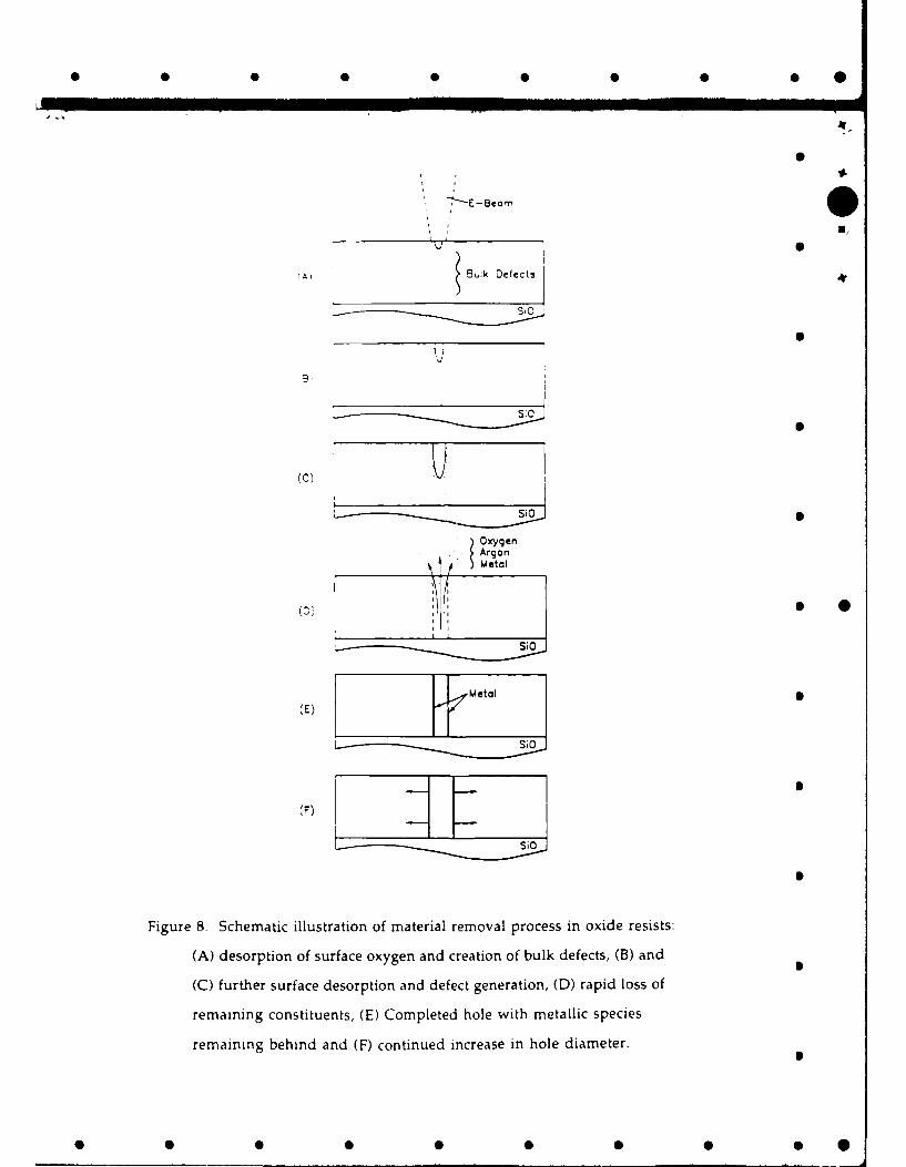
From the evidence above e ablative removal of material under e-beam
exposure appears to occur through a multiple step sequence of events starting
with desorption of surface oxygen and finishing with the rapid displacement
of bulk cation, oxygen and inert gas film components in the irradiated
volume. Figure 8 schematically illustrates the progression of hole
development believed to occur in oxide films beginning with: (A) the
desorption of oxygen from the surface and generation of defects in the bulk,
(B) and (C) continued surface desorption, (D) rapid expulsion of components
remaining in the irradiated volume and (E) and (F) the resulting hole which
retains metallic species at hole edges and which increases in size with
continued exposure.
.7
0S
0 0 S S S S S S •
The desorption of oxygen from surfaces and generatinm [ll hulk i,-it., t.
in oxide films is believed to occur simultaneously a, a reult il. tr,,
excitations produced by inelastic scattering ot incident e-beam ( )fi. '•,,d,
which is useful in describing desorption and defect generatlion in ,\idt-, ' ,
ESD theoryl-' . In this model, charge transfer in highly ioni, m,' i•.I
valence oxides occurs through an Auger decay proces.s and kan r ;n I ,
the loss of surface oxygen or displacement of bulk oxygen atoms tr,, ti.,
original electrostatic equilibrium position in the structure The, g.vnuratm,,•,,
0bulk oxygen and metal defects can be described by the defect equat•on, b,'.,
30o, = 3/2 02 + 3Vo + be
2AlA1 + 6e = 2 Almetad
Once bulk defects are formed a preferential diffusion of cation,, away irn ,
irradiated volume appears to occur. Evidence of the separation aMd
preferential diffusion of cations is found in the pres.ence (i rndur, d m•t..,* S
regions at hole edges. Electric field during c-beam exposure can , ilt t,
movement of cations away from the immediate area and aik, hinder .amdiffusion of negatively charged oxygen species remaynin .AI ltou ' ,
direct evidence exists that oxygen and argon art, the primary -t.,-it- in til,
irradiated volume, when the remaining material i, rapidly dci plad It.
of any oxygen or inert gas r( naming after exposure strongly -uppjrt thi'ý
Using FIELS, molecular oxygen peaks was reported to appear upon initial
exposure, which then disappear upon completion of the structure
It is still not clear what process may be controlling the final rapid
removal of material Linder irradiation, however, it is safe to assume that thi,
material must be in a highly defect and disordered state due to irradiation
damage. The produced oxygen and remaining volume may combine to form
molecular oxygen and the inert gas may coalesce to form bubbles. The
8 • S
volume expansion of gases formed in such a manner could be significant,
producing a region of high pressure, and result in a rapid expulsion of
material consistent with observation. Although no macroscopic evidence of 0
heating was observed, local heating from the relatively short duration high
intensity exposure could result in brief rapid expansion of material, in solid
or gaseous form, thereby generating a pressure capable of expelling material 0
from the hole. It is quite clear, however, that some critical point is reached, or
a critical volume of material is formed, which is associated with the final
rapid removal of material and formation of a complete hole.
The contrast response of polycrystalline and amorphous rf sputtered
films cannot be explained simply in terms of the initial damage mechanism
but rather indicates that microstructural characteristics are also extremely 0
important to the overall speed of the exposure process. Deposition of oxide
films at cryogenic temperature has produced structures which are not stable at
room temperature. This instability may help drive atomic rearrangement. 6 0
The relatively open structure of amorphous films is also believed to
significantly enhance the rate of bulk atomic diffusion. The greatly reduced
dose requirements of rf sputtered films relative to those produced by other
techniques is also strong evidence that both microstructural and chemical
characteristics strongly influence the rate at which material can be removed.
From the qualitative exposure model proposed above the total exposure time
or dose requirement of a given oxide resist should be dependent on the rate at
which surface species desorb and bulk defects can diffuse and finally be
displaced or expelled from the irradiated volume.
The parameters, such as film thickness, exposure parameters and inert
gas incorporation, which were found to primarily influence the dose
requirement in a given material are discussed below. 1hickness of the oxide
9
0 0 • S 0 0 0
I nnn n n •... .
a1
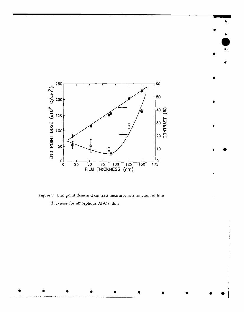
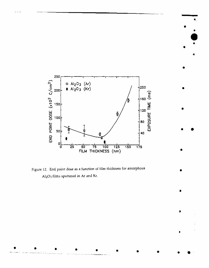
films was found to strongly affect the exposure dose requirement. Figure 6
shows the end point dose measured as a function of A120 3 film thickness
between approximately 15 and 150 nm. At film thickness greater than
approximately 100 nn it was found that the dose requirement begins to
increase, such that an optimum thickness occurs at 90 nm, where the film is
most sensitive. The contrast, reported as the percent change in transmitted
beam signal after exposure is also plotted in figure 9. This parameter is
important in data storage applications and over this thickness range should
be approximately proportional to film thickness, as observed. The influence
of film thickness on dose requirement is believed to involve the removal of
oxygen and inert gas remaining in the developing hole. If the film is very
thin, oxygen can be removed predominantly through surface desorption and
the critical volume and inert gas required for rapid expulsion may never be
generated. In very thick films (>100 nm) the larger amount of material which
must be removed and increased scattering of the incident electrons, appear to
result in a slower rate of final structure formation.
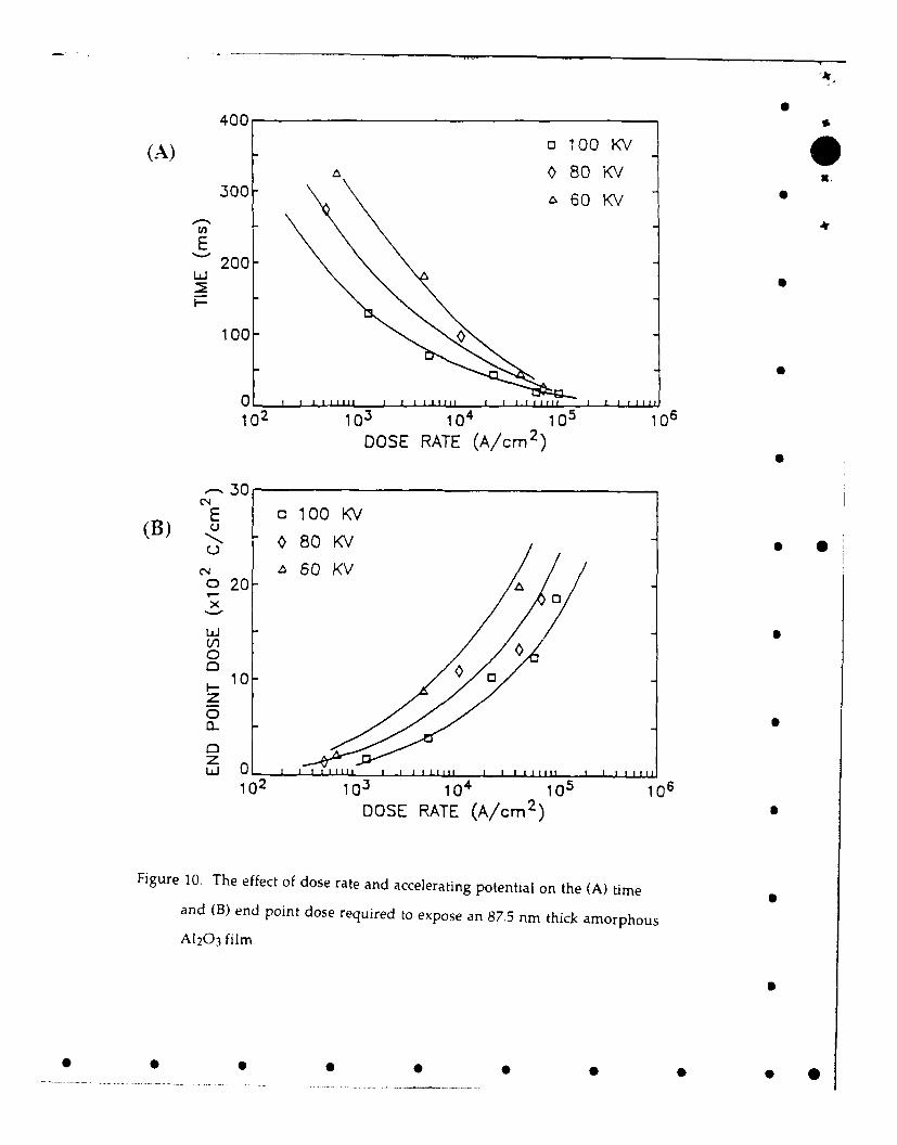
Two exposure parameters which can be strongly influence e-beam film
interactions are the dose rate and beam energy. The effect which dose rate
and beam energy had on the time and corresponding end dose required for
exposure of a single hole in an 87.5 nm thick A120 3 film is shown in figure 10.
The decrease in exposure time with increasing dose rate covered
approximately an order of magnitude between dose rates of 5x10 2 and IIO5
A/cm 2 . This decrease appears to result straightforwardly from the increased
number of electrons incident on the sample in a given time at higher dose
rates. However, the end point dose also increased as the dose rate increased.
This indicates that the total number of incident electrons required to
complete the exposure of a single hole increased as the rate at which electrons
1 0
S S • • 0 S • 5 0
impinge on the sample increases. In terms of the exposure model developed,
the probability for surface desorption and defect generation should not be X,p
dependent on dose rate. Therefore, the rate at which these events occur
should increase proportionately with dose rate. The bulk diffusion processes
which control the speed of material displacement in the bulk irradiated
volume should, however, be relatively independent of dose rate over this
range. Since there appears to be a critical volume of oxygen and inert gas
associated with the final removal of material and the completion of exposure,
the attainment of this critical condition will ultimately be controlled by the
time required for sufficient material diffusion to occur. As a result, the
diffusion of material within the bulk of irradiated film is believed to be the
rate controlling step in the exposure process. The increase of beam energy,
while not as significant as that of dose rate, does produce a factor of two
improvement in sensitivity at the higher accelerating potentials. * 0
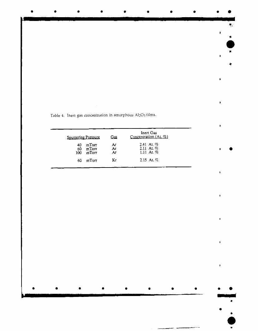
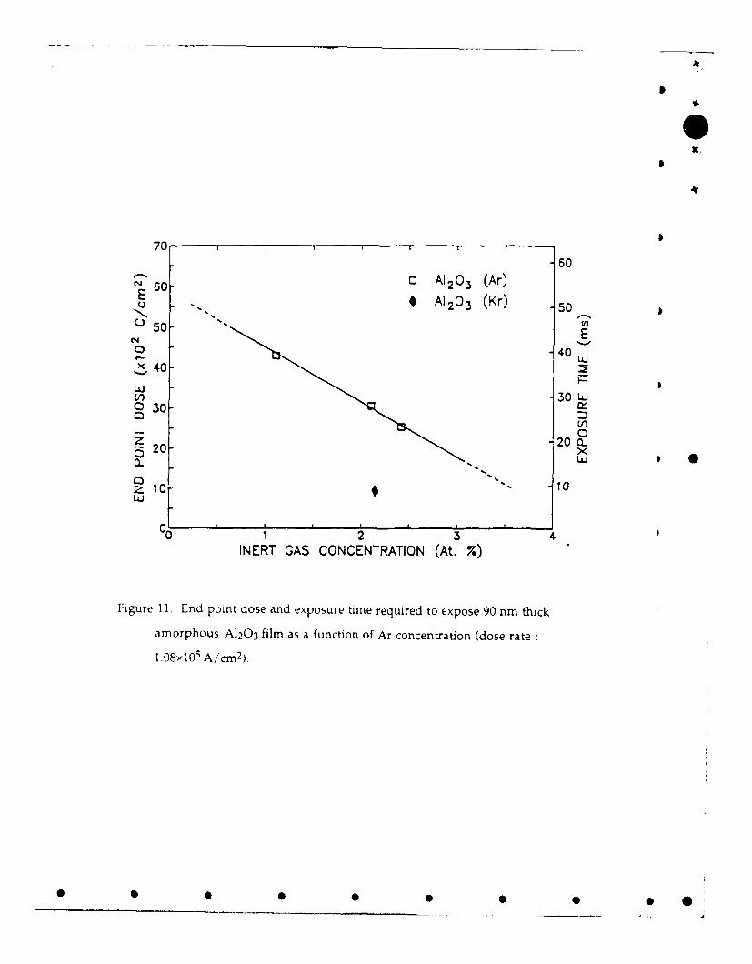
To isolate the effect of inert gas incorporation on the exposure
characteristics of the oxide films a series of 90 nm thick amorphous A1203
films containing various amounts of Ar were examined. These films were
deposited using different Ar pressure. These Ar concentration in the films
are given Table 4 and the Ar concentration increased as sputtering pressure
was decreased. In addition to Ar concentration, amorphous films produced
using a Kr atmosphere and incorporating Kr hi the structure was also
examined. Figure 11 shows the end point dose and time required for
complete exposure of amorphous A120 3 films as a function of Ar
concentration. The increment of Ar concentration resulted in huge
improvement of film sensitivity. Figure 12 shows the improvement in film
sensitivity using Kr. Kr, which has a larger atomic size compared to Ar,
II
S S S S S Now
A'
results in a measurable improvement in film sensitivity. These effect are
strongly related to the more open structure of amorphous films. IThe resolution of hole and line patterns was studied as a function of
film thickness and total exposure dose, using multiple dose / multiple 4
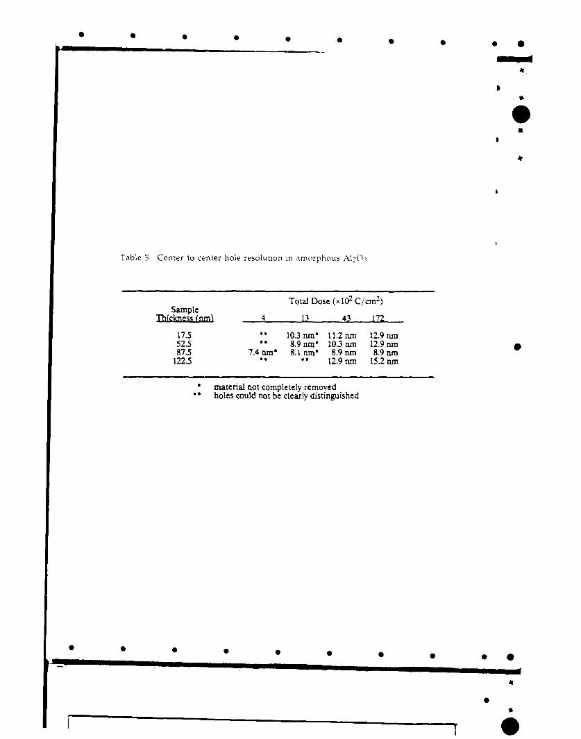
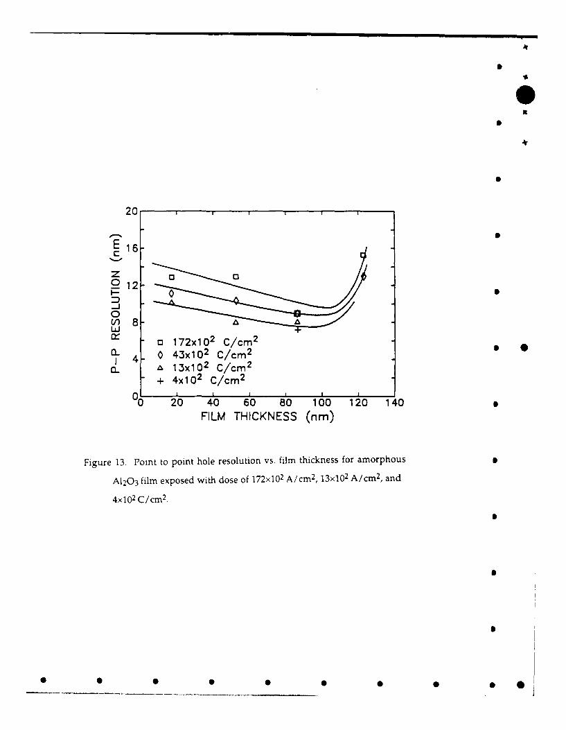
spacing patterns. Table 5 and figure 13 shows these effects. Optimum film
thickness was again found to occur at approximately 90 nm where 5.0 nm 0
holes could produced on 8.9 nm centers. Slightly better resolution is reported
at exposure doses of 13x10 2 and 4x10 2 C/cm 2, however, holes formed at these
doses did not result in complete material removal. 0
A number of factors are believed to contribute the final diameter of
holes produced in rf sputtered oxide films, including the spatial distribution
of electrons in the beam, divergence of the beam, noise in the exposure 0
system and the range of inelastic scattering events. The most significant
contribution is believed to be the noise in the exposure system which
produces variation in the beam position, Noise is not unusual in electron 40
beam systems and can arise from a number of sources, including external
mechanical, acoustic and magnetic sources, as well as from electrical and
mechanical instabilities in the system itself14 . Contributions from beam
divergence and the spatial distribution of electrons in the beam will also
contribute to exposure of material outside the nominal 1 nm diameter of the
incident beam but cannot alone account for the 5.0 nm diameter hole
produced in the optimized amorphous film. The range of inelastic scattering
events themselves should under ideal exposure conditions be the resolution
limiting mechanism1 5.
Conclusively, amorphous film structure was found to be a requirement
for rapid material removal to occur while material properties found to
influence irradiation response include ionic character, heat of formation and
12
I L A - A 6
AJ
melting point. The specific role of the material properties are not clear but
may involve the film growth processes and variations in final structure. As a 0
result of observation made, a format for predicting the response in new oxide
materials has now been established. Improvement in the lithographic
characteristics of high resolution oxide resists have been shown to be possible
through improved understanding of the exposure process. Figure 14 shows
also the possibility of applying this technique to other applications, such as
memory systems. This improved understanding, along with the
development of new materials, is expected to result in more widespread
application of these materials as the need for nanometer scale lithography
techniques continues to grow. 0
IV. Conclusions
1. A number of e-beam interactive high resolution oxide resist materials
have been developed, including A1203, Y20 3, Sc203, 3A1203.2SiO 2 , and
MgO.AI20 3 . These resists , produced by rf sputtering at cryogenic
temperature, can be exposed much more rapidly and with a lower dose than
materials prepared by other techniques.
2. The incorporation of Ar in amorphous A120 3 was found to decrease the
end point dose requirement, as the Ar concentration increased. Incorporation
of Kr at the same concentration was found to further decrease the end point
dose requirement.
3. High ionic character, high heat of formation and high melting point were
identified as desirable material characteristics.
4. A qualitative model of the exposure process has been developed. The
process was modeled as a sequence of events beginning with the desorption of
oxygen from the film surface and generation of bulk defects. Further surface
13 3
* 0 5 0 • 0 0 0 0 S
,4
• • •:j..,,•4-• • .,.;'t,,J~ • ••,,,,,,v'S
'4' a;•' • • '•• '•" ~ a4•,s*"tk•/
desorption and the diffusion of bulk defects is followed by a rapid expulsion O
of components remaining in the irradiated volume. Initial desorption and X,
defect generation is believed to result from electronic excitations produced by4.
inelastic scattering.
5. Film thickness was found to have a significant effect on the end point dose
requirements. The best result was obtained at approximately 90 nm. No
threshold current densities were observed in any of the films examined
under dose rates as low as 1X10 3 C/cm 2.
6. The high resolution of amorphous A120 3 films allowed the production of
5.0 nm holes on 8.9 nm centers and 8.0 nm lines on 12.0 run centers. Noise in
the exposure system was believed to limit the ultimate resolution.
V. Acknowledgments
We thank the staffs of Materials Research Labs for the use of the
equipment pertaining to this experiment. This work was supported by
DARPA under Office of Naval Research contracts No. N00014-88-K-0317 and
N0014-92-J-1868.
14
I
o
VI. Reference
1. A. N. Broers J. Cuomo J. Harper W. Molzen R. Laibowitz and M. 0
Pomerants, "High Resolution Electron Beam Fabrication Using STEM," 9th 4'
hIternational Congress on Electron Microscopy, III 343-354 (1978).
2. D. C. Joy, "The Spatial Resolution Limit of Electron Lithography," 0
Microelectronic Eng., 1 103-19 (1983).
I E. Kratschrner and M. Issacson, "Nanostructure Fabrication in Metals,
Insulators, and Semiconductors Using Self-Developing Metal Inorganic
Resists," 1. Vac. Sci. Technol., B4 361-4 (1986).
4. M. Issacson and A. Murray, "In Situ Vaporization of Very Low Molecular
Weight Resists Using 1/2 nm Diameter Electron Beams," J. Vac. Sci. Technol,
19 [411117-20 (1981).
5. M. E. Mochel J. A. Eades M. Metzger J. I. Meyer and J. M. Mochel, "Electron
Beam Cutting in Amorphous Alumina Sheets," Appl. Phys. Lett., 44 [51 502-5
(1984).
6. j. L. Hollenbeck and R. C. Buchanan, "Properties of E-Beam Interactive
Oxide Films," Mat. Res. Soc. Symrp., 72 289-294 (1986).
7. J. L. Hollenbeck and R. C. Buchanan, "Nanometer-Scale Structures
Produced in Oxide Films," Proceedings of the 45th Annual Meeting of the
Electron Microscopy Society of America, 396-7 (1987).
8- 1. G. Salisbury, R. S. Timsit, S. D. Berger, and C. J. Humphreys,
"Nanometer Scale Electron Beam Lithography in Inorganic Materials," Appl.
Phys. Lett., 45 [121 1289-91 (1985).
9. S. D. Berger, J. M. Macaulay, and L. M. Brown, "Radiation Damage in TiOx
at High Current Density," Phil. Mag. Lett., 56 [51 179-85 (1987).
15
S S 5 0 0 5 S 0 •
l M. L. Knotek and P. J. Fiebleman, "Stability of Ionically Bonded Surfaces
in Ionizing Environments," Snrface Science, 90 (78-90] (1979).
. M. L. Knotek, "Radiation Induced Surface Decomposition," Proceedings
of the 41st Annual Meeting of Electron Microscopy Society of America, 368-9
(1983).
12. M. L. Knotek, "Stimulated Desorption," Rev. Prog. Phys., 47 1499-1561
(1984).
13. S. D. Berger I. G. Salisbury R. H. Milne D. Imeson and C. J. Humphreys,
"Electron Energy-Loss Spectroscopy Studies of Nanometer -Scale Structures in
Alumina Produced by Intense Electron-Beam Irradiation," Phil. Mag. B, 55 [31
341-358 (1987).
14. E. Kratschmer, S. A. Rishton, D. P. Kern, and T. H. P. Chang,
"Quantitative Analysis of Resolution and Instability in Nanometer Electron
Beam Lithography," ]. Vac. Sci. Technol., B6 [6] 2074-79 (1988).
15. M. Isaacson and J. P. Langmore, "Determination of the Non-Localization
of Inelastic Scattering of Electrons by Electron Microscopy," Optik, 41 [1] 92-6
(1974).
16
• • •• • •• •
0~l I 0I 0I I I 0_ 1 nII Inl II I
i0
VII. List of Figures
X)
Table 1. Argon concentration in rf sputtered films. 0
Table 2. E-beam irradiation response in rf sputtered oxide thin film.
Table 3. Summary of oxide material properties.
Table 4. Inert gas concentration in amorphous A120 3 films.
Table 5. Center to center hole resolution in amorphous A12 0 3.
Figure 1. Schematic illustration of the 200 mesh coated copper grid used as a
support substrate for rf sputtered films.
Figure 2. TEM bright field image, corresponding SAD pattern and X-ray
spectra of rf sputtered (A) polycrystalline A120 3 and (B) amorphous
A1203 films.
Figure 3. (A) RBS and (B) SIMS spectra from amorphous A12 03 film.
Figure 4. Lithographic structures which have been produced in amorphous
films of (A) A120 3 and (B) 3A12 03 .2SIO 2 using e-beam irradiation.
Figure 5. Hole development in an 87.5 nm thick amorphous A12 0 3 film as
indicated by (A) a bright field image of a multiple dose/multiple
spacing pattern, (B) the resulting hole diameter as a function of
exposure time and (C) the transmitted signal during exposure of
three consecutive holes (dose rate: 1.08x10 5 A/cm2 ).
Figure 6. STEM bright field images of (A) amorphous A120 3 and (B)
3Al2O3.2SiO2 amorphous films in which redeposition of material into
adjacent structures was observed.
Figure 7. Microdiffraction patterns taken from regions near newly created
structures in (A) A1203, (B) Y20 3 and (C) ZrO 2 corresponding to patterns
of metallic Al, Y and Zr respectively.
17
• • • •• • •S
0 5 S ISIIN I nS mnn .. . . . . .. * ,,a. . . .
Figure 8. Schematic illustration of material removal process in oxide resists:
(A) desorption of surface oxygen and creation of bulk defects, (B) and U.
(C) further surface desorption and defect generation, (D) rapid loss of
remaining constituents, (E) Completed hole with metallic species
remaining behind and (F) continued increase in hole diameter.
Figure 9. End point dose and contrast measures as a function of film
thickness for amorphous A120 3 films.
Figure 10. The effect of dose rate and accelerating potential on the (A) time
and (B) end point dose required to expose an 87.5 nm thick amorphous
A120 3 film.
Figure 11. End point dose and exposure time required to expose 90 nm thick
amorphous A120 3 film as a function of Ar concentration (dose rate
1.08x10⁵ A/cm2).
Figure 12. End point dose as a function of film thickness for amorphous
A120 3 films sputtered in Ar and Kr.
Figure 13. Point to point hole resolution vs. film thickness for amorphous
A120 3 film exposed with dose of 172x10 2 A/cm2, 13x10 2 A/cm 2, and
4x10 2 C/cm 2.
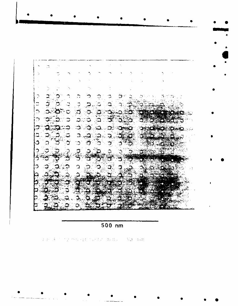
Figure 14. Dot patterns produced in amorphous A120 3 film.
18
400inn~lf KV
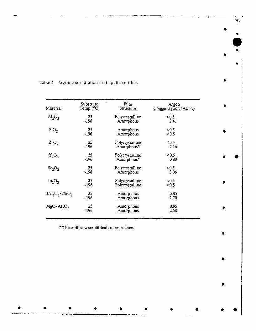
Table 1. Argon concentration in rf sputtered films.
Substrate Film ArsonMaterial Te.,O StrucMre Concentration (At. %7c)
A12 0 3 25 Polycrystalline < 0.5-196 Amorphous 2.41
SiO2 25 Amorphous < 0.5-196 Amorphous < 0.5
ZrO2 25 Polycrystalline < 0.5-196 Amorphous* 2.16
Y20 3 25 Polycrystalline < 0.5 * *-196 Amorphous* 0.80
Sc20 3 25 Polycrystalline < 0.5-196 Amorphous 3.06
In 2 0 3 25 Polycrystalline < 0.5-196 Polycrystalline < 0.5
3A12 0 3 .2SiO 2 25 Amorphous 0.85-196 Amorphous 1.70
MgO.AI2 0 3 25 Amorphous 0.95-196 Amorphous 2.58
"These films were difficult to reproduce.
• • •• • •• •

qiA'
Table 2. E-beam irradiation response in rf sputtered oxide thin film.
Initial Exposurea R Structre Size Dose Requirement
Polyerystalline:A120 3 none - -Y20 3 none - -ZrO, none - -SC2O3 none - -4n20 3 none - -
Amorphous:A120 3 rapid 5 rim 5 x 10, C/cm2
Y20 3 rapid 5 ran 5 - 10, C/cm 2
3A120 3.2SiO 2 rapid 5 rim 5 x 10³ C/cm2
MgO.A120 3 rapid 10 rim 5 x 10³ C/cm 2
Sc20 3 rapid 10 rim 5 x 10³ C/cm2
ZrO, slow 8 nm 1 . 106 C/cm 2
SiO 2 none -
0S
- - - - - - - - - - -
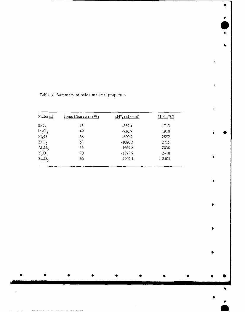
Table 3. Summary of oxide material propvrti_,5
SIonic Character %c•) =..f - -L.i o M .P. °i C
SiO 45 -859.4 1713In,0 3 49 -930.9 1910 *MgO 68 -600.9 2852
ZrO, 67 -1080.3 2715
A.10 3 56 -1669.8 2030
Y 103 70 -1897.9 2410Sc,0 3 66 -1902.1 > 2405
Sl
3
* *0 000 0 *
4,
i
Table 4. Inert gas concentration in amorphous A1203 films.
Inert Gas
Sputtering Pressure Gas Concentration (At. %)
40 reTorr Ar 2.41 At. %60 reTorr Ar 2.11 At.% ,
100 reTorr Ar 1.11 At. %
60 reTorr Kr 2.15 At. %
0 0 0 0 0 0 0
0
I
Table 5. Center to center hole resolution in amorphous Al2O-
Total Dose (x102 C/cmn)Sample
Thickness (nm) 4 13 43 172
17.5 "" 10.3 rim* 11.2 rim 12.9 nm52.5 8.9 8m" 10.3 am 12.9 nm87.5 7.4 rim 8.1 rim* 8.9 rm 8.9 rm
122.5 "" so 12.9 rum 15.2 rm
a material not completely removed• holes could not be clearly distinguished
0 0 0••
0
SI
0
• • • •• • •
* * S S S S S * 0 6
A
S
N
S
- 4
7S
S
2 0 0 nfl'
S
* 0
S
I S
S
I I \¶ vri�t�¶ i.�l � nrrt'���flhIn� �-'�\I ) p�tt�rn �ind \-rd\
-� rt � � *��h re I \ I'�U\ r\�t�iIifl�' \I � i-b ,Irndrphdlis
N 4
S
* 5 0 5 S S S S 5 6
Energy (MeV)0.0 0.2 0.4 0.6 0.8 1,0 1.2 1.4
M 1.0 5 1.5 *4
1 0.8 Ar
50-
40'ýZgo0.2
0 0,880 700 740 780
Channel
ASi
•~~~~
2oOS e
H *A
Aý2 0 3 +Ar-
SeV 4He+ Ar
0 200 400 600 800
Channel
A .[2 0 3
S i O
F o r m nv a r
Film Substrate Cu-Grid
Cu
0
Si
S10
"102 0
L"l
10' C I
I I ,
0 200 .oQ 600 goo 1000 1200
Time (sec)
Figure 3. (A) RBS and (B) SIMS spectra from amorphous A1203 film.
S
•
5 5
0 5
0 * 0
1.04
elS
(A) UFM &
LS
hthor~ihic rucurc, whch m~c eci prducc inalmi-I'lml
t I II t : I II L (B)I., I c-bcom i ra I t i(it
* S S5 0 S 000
x~n4
FF
-.- ~-i
lai WK.
SEEM7EME~
(x-axis: 10 mns/div.)
(c)
1\ p1 sc nrte nul and v t wid mm,',c (tte 1g1 J lt Ic do 1 -( IkItik
p, (r I I I) ,. til 1)tI ss ~ II ~
, S~ 5 0 5 S S S 5
0 0 00 S SS S
Aluminum: ti[ll)
Yttrium B[00011
Zirconium B3 1 12131
lFigure 7, %icrodiftraction patterns, takeni fromn regions near niewlY Created
structures, iii (A) AV( 13, (B) Y2( ¾ and (C) Zr()' corresponding to patterns
of ni(ta1lllc Al, Y and Zr respectively,
Bulk Defects
(C)
Sio
*Oxygen*Argon
"SI
Metal e
(E)
~SO
BS
(F)
Figure 8. Schematic illustration of material removal process in oxide resists:
(A) desorption of surface oxygen and creation of bulk defects, (B) and
(C) further surface desorption and defect generation, (D) rapid loss of
remaining constituents, (E) Completed hole with metallic species
remaining behind and (F) continued increase in hole diameter.
S 0
mm"
U,
250 , 60
Eu -50S200C-)
C14 .4 0 •x 150 "-
10o Io
o 100 z-203
z0nL 50- 10
z0 I I I I I 0
0 2s 50 75 100 125 150 175
FILM THICKNESS (nm)
Figure 9. End point dose and contrast measures as a function of film
thickness for amorphous A12 0 3 films.
0 0 0 0 • 0 0 0 0 0
400
(A) o 100KV
.0 80KV X,300. 60 KV
m~4'E
200
100
0 n1 1 1 1nnnii 1 t ! tf__l I I f illt I I I # it ))
10 2 103 104 105 06DOSE RATE (A/cm 2 )
,, 30C'N
E a 100 KV( 0 80KV aC-)
04 60 KVC 20A
x0
wi S(A00
10z0~
0z
102 103 1041 5 106DOSE RATE (A/cm2 )
Figure 10. The effect of dose rate and accelerating potential on the (A) time
and (B) end point dose required to expose an 87.5 nm thick amorphous
A120 3 film.
0 0 0
7060
60- c A1203 (Ar)U 60 A1203 (Kr) 5IN 0 50
-40
ULU
Ln 30 W0130
70
60
S60 200..3 ArS ) U
O 1 203 4INERT GAS CONCENTRATION (At. %)
Figure I1I End point dose and exposure time required to expose 90 nm thick
amorphous A120 3 film as a function of Ar concentration (dose rate
1.08xi0 5 A/cm2).
0 40 0 S00
0
250
4 3 A12 0 3 (Ar)E - 0200 A12 0 3 (Kr)S200 ,-.
S~Eo'o m 8o"-04 -160~
x 150 L,
LAJ -120Lii
o 100 - s
z C_0 80 J
z #j 0 -
0 25 50 75 100 125 150 175FILM THICKNESS (rim) S
Figure 12. End point dose as a function of film thickness for amorphous
A1203 films sputtered in Ar and Kr.
• • • •• • •
20
E 16-
12-
-ji
X - o 172x10 2 C/cm'-4L 0 43x1 02 C/cm2
CL 13x10 2 C/cm2
+ 4x10 2 C/cm2
OL 2'0 4'0 6'0 130 1060 120-' 14 0FILM THICKNESS (nm)
Figure 13. Point to point hole resolution vs. film thickness for amorphous
A12 03 film exposed with dose of 172xl02 A/cm2, 13x10 2 A/cm2, and
4x 10² C/cm2.
Lon 6 0 0 0 0 * 0
"I 0
o or
IL -35
500 n