Embed Size (px)
Citation preview

I
m^im^mmmmMmmM^MimmMmmä^MMmmMmik
ANNUAL REPORT
SiC Discrete Power Devices
Supported Under Grant # N00014-96-1-0363 Office of Naval Research
Funded by ONR Program Scientific Officer: Dr. John Zolper
Report for the Period of January 1,1999 through December 31,1999
Principal Investigator: Professor B. Jayant Baliga
Department of Electrical and Computer Engineering Power Semiconductor Research Center
North Carolina State University Campus Box 7924
Raleigh, North Carolina 27695-7924
SHC QUALITY INSPECTED 3
I 20000106 090

REPORT DOCUMENTATION PAGE Form Approved OMB No. 0704-0188
Public reporting burden for this collection of information is estimated to average 1 hour per response, including the time for reviewing instructions, searching existing data sources, gathering and maintaining the data needed, and completing and reviewing the collection of information. Send comments regarding this burden estimate or any other aspect of this collection of information, including suggestions for reducing this burden, to Washington Headquarters Services, Directorate for Information Operations and Reports, 1215 Jefferson Davis Highway, Suite 1204, Arlington, VA 22202-4302, and to the Office of Management and Budget, Paperwork Reduction Project (0704-0188), Washington, DC 20503.
1. AGENCY USE ONLY {Leave Blank)
2. REPORT DATE January 1, 20*»
3. REPORT TYPE AND DATES COVERED Annual!/1/99-12/31/99
4. TITLE AND SUBTITLE SiC Discrete Power Devices:
AUTHORS R. K. Chilukuri, B. J. Baliga
FUNDING NUMBERS 97PR00099-00 N00014-96-1-0363 N68892
N66020 4B855
7. PERFORMING ORGANIZATION NAME(S) AND ADDRESS(ES) North Carolina State University Hillsborough Street Raleigh, NC 27695
8. PERFORMING ORGANIZATION REPORT NUMBER
N00014-96-1-0363-1
SPONSORING / MONITORING AGENCY NAME(S) AND ADDRESS(ES) Sponsoring: ONR, Code 312, 800 North Quincy, Arlington, VA 22217-5660 Monitoring: Administrative Contracting Officer, Regional Office Atlanta Regional Office Atlanta, 101 Marietta Tower, Suite 2805,101 Marietta Street Atlanta, GA 30323-0008
10. SPONSORING/MONITORING AGENCY REPORT NUMBER
11. SUPPLEMENTARY NOTES
12a. DISTRIBUTION/AVAILABILITY STATEMENT Approved for Public Release, Distribution Unlimited
12b. DISTRIBUTION CODE
13. ABSTRACT (Maximum 200 words)
A novel planar vertical MOSFET structure (called ACCUFET), which eliminates both the problems of premature oxide breakdown and low inversion layer mobility, has been demonstrated by us. Here, the studies done at the Power Semiconductor Research Center for design and development of ACCUFETs are documented. The characteristics of ACCUFETs fabricated from 6H-SiC and 4H-SiC polytypes with measured breakdown voltages of 350^*50 V, are compared. The 6H-SiC ACCUFETs exhibited excellent electrical characteristics, while the performance of 4H-SiC ACCUFETs was worse than expected. The investigation of the poor performance of the 4H-SiC ACCUFETs provided insights for changes in device design and process flow, for improving their breakdown voltage and specific on-resistance. Further, characteristics of Ni/4H- SiC Schottky rectifiers operating at 1.5 to 2.5 kV using low energy Ar implants for edge termination are reported. Apart from being a detailed study of the performance of 4H-SiC high voltage Schottky barrier diodes, the characterization of these diodes also provided insights on the quality of the starting material, the barrier heights and the edge termination, that contributed to the proposed new ACCUFET fabrication run. In addition, the effect of key device design parameters on device characteristics have been studied with the help of two-dimensional simulations.
14. SUBJECT TERMS silicon carbide, ACCUFET, Schottky rectifier, specific on-resistance, breakdown voltage
15. NUMBER OF PAGES 40
16. PRICE CODE
17. SECURITY CLASSIFICATION OF REPORT unclassified
18. SECURITY CLASSIFICATION OF THIS PAGE unclassified
19. SECURITY CLASSIFICATION OF ABSTRACT unclassified
20. LIMITATION OF ABSTRACT SAR
NSN 7540-01-280-5500 Standard Form 298 (Rev. 2-89) Prescribed by ANSI Std. Z39-1 298-102

Table of Contents
1. Introduction 1
2. A Comparison of 6H-SiC and 4H-SiC ACCUFETs 3 2.1 Introduction 3 2.2 ACCUFET Device Structure and Fabrication 4 2.3 Comparison of 6H-SiC and 4H-SiC ACCUFETs 4 2.4 On the issue of improving breakdown voltage 9 2.5 On the issue of improving specific on-resistance... 13 2.6 Conclusion 14
3. High Voltage Ni/4H-SiC Schottky Rectifiers 16 3.1 Introduction 16 3.2 Device Fabrication 16 3.3 Results and Discussion 18 3.4 Conclusions 21
4. Device Design and Simulation 25 4.1 Introduction 25 4.2 Device Structure and Operation 25 4.3 Electric Fields 26
4.3.1 Effect of JFET width 26 4.3.2 Trade-off with forward voltage drop 28
4.4 Current density-Voltage (J-V) Characteristics 29 4.4.1 Effect of JFET width 29 4.4.2 Effect of channel length 29 4.4.3 Effect of gate bias 29
4.5 Specific On-Resistance 34 4.5.1 Analytical model 34 4.5.2 Effect of JFET width 36 4.5.3 Effect of channel length 36 4.5.4 Effect of gate bias 37
5. Conclusion 39

1. Introduction
The specific on-resistance of SiC FETs has been projected to be 100X lower than Si devices. Due to very low diffusion coefficients in SiC even at high temperatures, the UMOS structure has been used to fabricate 4H-SiC MOSFETs with breakdown of 1.1 kV [1]. In a SiC UMOS structure, high electric field at the trench corners leads to catastrophic failure of the gate oxide at high drain voltages [2], which restricts the maximum operating voltage to much below the plane parallel breakdown voltage. Further, the extremely low (1-7 cm2/V-s) inversion layer mobility observed in the SiC UMOS devices leads to a high specific on-resistance for the device, which nullifies the advantage of the low drift region resistance. A novel planar vertical MOSFET structure (called ACCUFET), which eliminates both the problems of premature oxide breakdown and low inversion layer mobility, has been demonstrated by us [3]. In this report, we document the studies done at the Power Semiconductor Research Center for design and development of ACCUFETs.
In section 2, we compare the characteristics of ACCUFETs fabricated from 6H- SiC and 4H-SiC polytypes with measured breakdown voltages of 350-450 Volts. The 6H- SiC ACCUFETs exhibited excellent electrical characteristics, while the performance of 4H-SiC ACCUFETs was worse than expected. The investigation of the poor performance of the 4H-SiC ACCUFETs provided insights for changes in device design and process flow, for improving their breakdown voltage and specific on-resistance. These insights and the subsequent changes incorporated in a proposed new ACCUFET fabrication run are also presented in this section.
In section 3, characteristics of Ni/4H-SiC Schottky rectifiers operating at 1.5 to 2.5 kV using low energy Ar implants for edge termination are reported. Apart from being a detailed study of the performance of 4H-SiC high voltage Schottky barrier diodes, the characterization of these diodes also provided insights on the quality of the starting material, the barrier heights and the edge termination, that contributed to the proposed new ACCUFET fabrication run.
Our new fabrication run is aimed at making ACCUFETs on 4H-SiC material of epilayer thicknesses varying from 10 urn to 40 urn, which correspond to breakdown voltages ranging from 2000 V to 7500 V. To facilitate an appropriate design matrix, the effect of key device design parameters on device characteristics have been studied with the help of two-dimensional simulations using MEDICI. These device simulations are discussed in section 4.
References:
1. A. K. Agarwal, J. B. Casady, L. B. Rowland, W. F. Valek, M. H. White, and C. D. Brandt, "1.1 kV 4H-SiC power UMOSFETs," IEEE Electron Device Lett., vol. 18, pp. 586-588, Dec. 1997.

J. W. Palmour, R. Singh, L. A. Lipkin, and D. G. Waltz, "4H-silicon carbide high temperature devices," in Trans. 3rd Int. Conf. High-Temperature Electronics (HiTEC), 1996, vol. 2, pp. XVI-9-14. P. M. Shenoy and B. J. Baliga, "The planar 6H-SiC ACCUFET: a new high-voltage power MOSFET structure," IEEE Electron Device Lett., vol. 18, pp. 589-591, Dec. 1997.

2. A Comparison of 6H-S1C and 4H-SiC ACCUFETs
2.1 Introduction SiC FETs have been projected to have a 100X lower specific on-resistance than Si
devices. As a consequence, the on-state voltage drop for even the high-voltage FET is much smaller than for any unipolar or bipolar silicon device. These switches are expected to switch off in less than 10 ns and have superb FBSOA [1]. Previously, the UMOS structure has been used to fabricate SiC MOSFETs because of very low diffusion coefficients in SiC even at high temperatures [2,3]. However, in a SiC UMOS structure, high electric field at the trench corners leads to catastrophic failure of the gate oxide at high drain voltages, which restricts the maximum operating voltage to much below the plane parallel breakdown voltage. Further, the extremely low (1-7 cm2/V-s) inversion layer mobility observed in the SiC UMOS devices leads to a high specific on-resistance for the device, which nullifies the advantage of the low drift region resistance. A novel planar vertical MOSFET structure (called ACCUFET), which eliminates both the problems of premature oxide breakdown and low inversion layer mobility, has been demonstrated [4]. ACCUFETs have been fabricated from 6H-SiC and 4H-SiC polytypes at Power Semiconductor Research Center [5]. Vertical MOSFETs fabricated from 4H-SiC are expected to show much lower specific on-resistance than those from 6H-SiC, due to a much higher (~10X) drift region electron mobility in 4H-SiC than in 6H-SiC. However, after fabrication, the 6H-SiC ACCUFETs exhibited excellent electrical characteristics, while the performance of 4H-SiC ACCUFETs was worse than expected. In this chapter, the electrical characteristics of the fabricated 6H-SiC and 4H-SiC ACCUFETs are compared. In addition, the investigation of the poor performance of the 4H-SiC ACCUFETs that provided insights for changes in device design and process flow, for improving the breakdown voltage and specific on-resistance is presented, and the subsequent changes incorporated in a proposed new run are listed.
MOSGate
^H .-■;.-■.■■■■ - ' ■■■-&>■
N+ I. Lch _|
/ N-
P+ \ WjcW2
r~
N-
N+ . ■
Drain
(a) (b)
Fig. 2.1 Schematic sketch of (a) cross-section and (b) top view of the planar SiC ACCUFET.

2.2 ACCUFET Device Structure and Fabrication Fig. 2.1 shows the cross-section of the proposed structure. The thickness and
doping of the N layer below the gate oxide is chosen such that it is completely depleted by the built-in potentials of the P7N" junction and the MOS gate, resulting in a normally-off device with the entire drain voltage supported by the P+/N" drift junction. The device is expected to have high breakdown voltage as this implanted P+/N" junction can support high voltages. The structure also utilizes the buried P+ region to suppress the electric field below the gate oxide, thereby preventing oxide rupture. When a positive gate bias is applied, the electrons flow through an accumulation channel created at the SiCVSiC interface. Since the accumulation layer mobility is expected to be higher than the inversion layer mobility, a lower on-resistance is expected for the proposed device. In order to verify the device operation, two dimensional numerical simulations were done using MEDICI. Simulations predicted that, with Wjch < 4 (im, the peak electric field in the gate oxide can be kept below 3.5 MV/cm even at a high drain bias of 1000V, thus preventing the oxide rupture problem observed in UMOSFETs [2,3].
An 8 mask process was developed to fabricate the high voltage planar ACCUFETs [5]. The starting wafers for both 6H- and 4H-SiC were single crystal N-type (3x1018 cm'3) substrates with a 10 u.m thick nitrogen doped (lxlO16 cm"3) epilayer. The buried junction was formed by a single high energy (380 KeV) boron implantation at a dose of lxlO14 cm" 2, using a 1.2 u.m thick deposited oxide as the mask. Monte Carlo simulations using SUPREM III predicted a channel thickness of about 0.3 urn and a junction depth of 0.7 um This implant was followed by multiple lower energy boron implants at the pad area so that contact could be made to the buried layer and at the periphery to isolate the source from the drift region at the edges of the device. Multiple energy (40,100 KeV) nitrogen implants at a dose of 8x1014 cm'2 were introduced to form the N* source regions. All implants were annealed at 1400 °C in argon for 30 minutes. After a standard RCA clean, the gate oxide (12.5 nm for 6H-SiC and 16 nm for 4H-SiC) was thermally grown using wet oxidation at 1100 °C followed by re-oxidation at 950 °C to reduce D;t and Qf [6]. A 0.5-um thick polysilicon was deposited by LPCVD and doped with phosphorous at 875 °C. The polysilicon was patterned using SF6/02 RIE and isolation oxide was thermally grown on the patterned polysilicon. Ti/Al was used to form both front and back side ohmic contacts. The ACCUFETs were fabricated with interdigitated linear geometries using 2-um design rules.
2.3 Comparison of 6H-SiC and 4H-SiC ACCUFETs All the characterization was done with the buried P+ layer shorted to the source.
Excellent I-V characteristics (Fig. 2.2) were obtained on the fabricated planar 6H-SiC ACCUFETs with good current saturation and gate control. Both the specific on- resistance (Ron,sP) and the saturation current increased with the temperature. A room temperature Ron,9p of 18 mQ-cm2 was measured on the best 6H-SiC device (cell pitch = 21 urn, Wjch = 4 pirn and Lch = 2.5 |im) at a logic level gate bias of only 5V, which was in excellent agreement with 15 mQ-cm2 obtained in simulations. In contrast, most of the previous SiC MOSFETs have used high-voltage (> 25V) gate drive in order to obtain good on-state conduction. In spite of using a low gate voltage, the measured specific on-

Wjch=3um Active area=2.52xl(T cm*
Vg=5V
25
Drain Voltage (V)
Fig. 2.2 Effect of temperature on the output characteristics of a 6H-SiC planar ACCUFET.
resistance of our 6H-SiC ACCUFETs is lower than that of the best 6H-SiC 50V UMOSFETs (38 mQ-crn2) [7] and the best 6H-SiC DIMOSFET (510V, 66 mQ-cm2) [8]. The measured Ro„,sp for the 6H-SiC ACCUFET is within 2.5X of the measured drift region resistance which is the best value obtained so far for any high voltage SiC MOSFET. Further, this Ron,sp is 30x lower than that of a 1500V Si MOSFET. The forward voltage drop of this device at 50 A/cm2 was 0.9V, which is much less than that of a 1200VIGBT (typically 3 V for a high speed device).
!
CO
180
160
140
120
100
80
60
40
20
No source metal fingers
n=1.7:
n=1.82-
250 300 350 400
Temperature (K)
6H-SiC Vg=5V.
80
f 60 G
40 1
20 £
a
450 500
Fig. 2.3 Specific on-resistance variation with temperature in 6H-SiC planar ACCUFETs with and without metal fingers on the source.

For obtaining a low R<,n,sp, it is important to keep metal contacts on N* source fingers. Sqme designs of ACCUFETs had metal finger contacts on the N* source, while others had a metal contact on the N* source pad area only. The devices with source metal fingers had low R«^ (<25 mQ-cm2), whereas those with remote source contacts had higher Ron,sp (-200 mQ-cm2) because of a high N* sheet resistance. The variation of Ron,* as a function of temperature was measured. The devices with source metal fingers exhibited a positive temperature coefficient whereas those which had remote source contacts showed a negative temperature coefficient.
-3
6HSiC
Device#53o261
>^g/Vta (300K)=O.76V <y Vta(450IQ=O.33V
lina^OOK^nOcrrf/Vs
|Jna(450K)=132cm2/Vs
300K
350K
400K
450K
0 1 2 3 4 5 6
Gate Voltage (V)
Fig. 2.4 Dependence of measured transfer characteristics of a 6H-SiC planar ACCUFET on temperature.
The Ron,sp of the devices with source metal fingers had a temperature dependence of T" where n varied from 1.4 to 1.73 for the different devices. The drift region Ron,sp measured from the test elements showed a positive temperature coefficient with an n value of 1.82. The Ron,sP of the device had a smaller temperature dependence than that of the drift region, indicating that contributions from other resistance components such as the channel, contact and substrate resistances collectively have a lower temperature dependence («<1.82). Further, although the electron mobility in 6H-SiC varies as T" where n =2.5, the R^p did not increase with an n value of 2.5 because of the increase in the carrier concentration due to the improved dopant ionization at higher temperatures. It is important to be noted that unlike previous SiC MOSFETs, these devices have a strong positive temperature coefficients for on-resistance. A positive temperature coefficient is extremely desirable since it allows paralleling of devices and also improves reliability by avoiding current filamentation problems. In contrast, the devices with remote source contact had a slight negative temperature coefficient, which was attributed to a negative temperature dependence (w=-1.25) of the N* source sheet resistance.
The threshold voltage Vu and the accumulation channel mobility Una were extracted from the measured transfer characteristics (Fig. 2.4). The threshold voltage

decreased from 0.76V at room temperature to 0.33V at 450 K (- -3 mV/°C). Thus, the 6H-SiC planar ACCUFET is a normally-off device throughout the temperature range. Further, this reduction in the threshold voltage with temperature contributes primarily to the increase in saturation current as observed in Fig. 2.1. The effective accumulation channel mobility increased slightly temperature from 120 cm2/V-s at 300K to 132 cm2/V-s at 450K. However, on a similar device, the accumulation channel mobility decreased slightly from 125 to 120 cm2/V-s for the same temperature range.
<
0.20
0.15
s
| 0.10 u e 2 0 0.05
0.00
. Vgs = 5V
■ ■ ■ • f • ■ ■ ■ *
■ Vgs = 4V
0.00
4frSiC Device UÜ518 T = 293K T = 450K
Active area = 2.64e-4 cm
0.25 0.50
Drain Voltage (V) 0.75
Vgs°3V
1.00
Fig. 2.5 Effect of temperature on the on-state characteristics of a 4H-SiC ACCUFET.
These changes were too small and fell within the measurement and extraction error and hence, no definitive trend in the effective accumulation channel mobility with temperature could be obtained. Thus, the accumulation channel mobility in these devices is inferred to be independent of temperature, unlike inversion layer mobility which increases rapidly with temperature.
The I-V characteristics of the 4H-SiC ACCUFET exhibit larger R^ (Fig. 2.5) than the 6H-SiC ACCUFET. The room temperature Ron,sp for the best 4H-SiC device was found to be very high (3.2 Q-cm2 at a gate bias of 5V), but reduced rapidly with increase in temperature to 128 mQ-cm2 at 450 K (Fig. 2.6(a)). The reduction in Ron,sp of the 4H- SiC devices was found to be due to an exponential increase of the effective channel mobility from 0.06 cm2/V-s at room temperature to 2.3 cm2/V-s at 450 K (Fig. 2.6(b)). The specific on-resistance is expected to be lower for devices fabricated on 4H-SiC wafers than those on 6H-SiC wafers due to the higher bulk mobility for electrons. Measurements on the test elements showed that as expected, the drift region resistance is indeed lower on the 4H-SiC wafers (0.9 mQ-cm2 vs 7.7 mQ-cm2 for 6H-SiC). Hence, it was concluded that the high resistance is most probably caused by the channel. The SIMS profile of the

8
deep boron implant indicated that the desired N-layer is formed for 6H-SiC. However, the SIMS profile exhibited a "shoulder" near the SiC/Si02 interface for 4H-SiC [9]. This indicates that the surface may have been inverted to P-type for 4H-SiC, which suggests formation of an inversion channel in the 4H-SiC MOSFET during the on-state. The increase in effective channel mobility with temperature for 4H-SiC is believed to be caused by interface states which trap electrons from the inversion layer.
3500 10.0
3000 -\ I Device zlS§18 X 4H-SiC
«C 2500 u E
■| 2000
■§ 1500 \ 4H-SiC
E
1
1.0
A\.
\
®l 1000 \ 1 0.1 f* \ 1 : (l,„=Aexp(-Ea/kT) *\
500 —*\ § A = 2092 cm2/V.s
o 6H-SiC *--♦-_-
B ÜB IB w
E. = 0.26eV
300 350 400 450 0.0 ' ' ' ' ' 2.0 2.4 2.8 3.2 3.6
Temperature (K) 1000/Temperature (1/K) (a) (b)
Fig. 2.6 (a) Effect of temperature on the specific on-state resistances in 6H- and 4H-SiC planar ACCUFETs. (b) Variation of effective mobility in a 4H- SiC planar ACCUFET with temperature, exhibiting Arrhenius-type dependence.
At room temperature, the unterminated 6H-SiC and 4H-SiC devices had a breakdown voltage (BV) of 350V and 450V, respectively, with a leakage current of < 100 U.A. There was no deterioration in the B V with repeated measurement on the same device as long as the current at breakdown was limited to 5mA (20A/cm2). The gate current was < 1 nA during the device breakdown. Hence, unlike the SiC UMOSFET, no evidence of oxide rupture was observed at breakdown in the SiC ACCUFET. Breakdown voltage of the buried P+/N" junction improved from 510V to 1240V on using an Ar implant edge termination [10], indicating that breakdown voltages of 1240V are obtainable from the epitaxial material used for fabricating the above ACCUFETs.
The effect of temperature on the breakdown voltage and the leakage current of a 6H-SiC planar ACCUFET is shown in Fig. 2.7. The breakdown voltage was observed to reduce linearly with temperature from 315 V at room temperature to 279 V at 200 °C. The rate of decrease in the breakdown voltage averaged about 0.21 V/°C, which

corresponded to a decrease in breakdown voltage of about 11% from room temperature to 200 °C. The leakage current, measured at a drain bias of 100 V, increased non-linearly from 0.33 uA at room temperature to 4.0 uA at 200 °C.
100 150 Temperature ( C)
Fig. 2.7 Effect of temperature on the breakdown voltage and leakage current of a 6H-SiC planar ACCUFET.
In Fig. 2.8, we plot specific on-resistance and breakdown voltage of 6H- and 4H- SiC ACCUFETs. For reference, lines describing the variation of specific on-resistance with breakdown voltage are included for real Si devices, ideal Si limit and ideal SiC limit at both 25 °C and 175 °C. The unterminated 4H-SiC ACCUFET (3.2 fl-cm2, 450V) is above the Si limit at room temperature. However, at 175 °C, this device is better than the real Si devices, assuming no change in the breakdown voltage. At this temperature, after edge termination, the 4H-SiC ACCUFET is about 1 OX better than the best Si device. The unterminated 6H-SiC ACCUFET is at the Si limit even at room temperature. After edge termination, this device is 100X better than the best Si device.
2.4 On the issue of improving breakdown voltage The breakdown voltage of the as-is ACCUFETs on 6H-SiC and 4H-SiC was about
350 V and 450 V, respectively. However, this is only about 30% of the ideal parallel- plane breakdown voltage (approximately, 1500 V). Hence, different edge terminations were investigated to determine the ways of improving the breakdown voltage.
Some of the devices were terminated by a Schottky contact (Fig. 2.9)formed with the lightly doped n-type epilayer by deposition of 3500 A of Titanium followed by 5000 A of Aluminum. The Schottky contact at the edge spreads the depletion at the edge and relaxes the electric field crowding, which can result in near-ideal breakdown voltages. However, the breakdown voltage of such a device in 6H-SiC and 4H-SiC was 360 V and 460 V, respectively. Measurements on test structures revealed that titanium formed a very poor Schottky contact with the epilayer, possibly due to poor epilayer surface before metallization.

10
10«
Ti 103
d E 's 10*
101 I s o
c '8 io° a »a
lfr« 10
tfÄ-SiC
Si limit
Real Si devices
100 1000
Breakdown Voltage (V)
10000
E u d « w e eg
10s
104
103
« 102
4) 06
u IS "S a
CO
101
10°
to-1
4HSUC
PSRC
Real Si devices
Real Si devices (25
*t PSRC (175% (projected)
4H-SiC limit (25 °C)
4H-SJC limit (175 °C)
10 100 1000
Breakdown Voltage (V)
10000
Fig. 2.8 Performance of 6H-SiC and 4H-SiC planar ACCUFETs.

11
Terminations without Amorohization Terminations with Amorphization
6H-SiC :360 V 4H-Sie:460Vl ^(Buried) 6H-SiC :370 V
AmorpMzed SiC
6H-SiC :330 V 4H-SiC :480 V
6H-SiC :390 V 4H-SiC :480 V
Pt-(Sinker)j
I^(Buriedj
Amorphized .SiC
Fig. 2.9 Breakdown voltages of 6H-SiC and 4H-SiC ACCUFETs after various edge terminations.
An edge termination that has resulted in near-ideal breakdown voltages in Schottky barrier diodes is the amorphization by argon ion-implantation [10]. This technique is based on creation of a thin high-resistivity layer on the surface at the edges of the device using high dose ion-implantation. With the application of a reverse bias, this high-resistivity layer promotes the spreading of the potential along the surface which results in reduced edge electric field. Hence, on some of the devices, the silicon carbide surface beyond the Schottky contact edge was amorphized using argon implants at an energy of 30 keV and a dose of lxlO15 cm"2. The breakdown voltage of these devices was the same as those of unterminated devices. Breakdown voltage was also measured on devices which did not have a Schottky metal on the edge and the amorphization extended to the P+ sinker isolating the device. The breakdown voltage of such a device in 6H-SiC and 4H-SiC was 390 V and 480 V, respectively.
This edge termination was not effective with the ACCUFET for the following reasons. The ACCUFET was designed such the P+ sinker and the buried P+ layer can be biased only at a small contact pad located at one edge of the device, and the edges (P+ sinker) of the device are far from the active device area (Fig. 2.10). Hence, when the pad is biased, there is considerable voltage drop between the pad and the edge, which if further enhanced if the conductivity of the P+ region is low due to the poor activation of the dopants. This large voltage drop and a poor Schottky barrier contact of the edge metal result in minimal potential spreading at the high resistivity amorphized region. Hence, the edge electric field does not reduce much, which renders the edge termination ineffective.
The effectiveness of this edge termination for an ACCUFET is proposed to be improved in a new device fabrication run by incorporating the following changes in the device design and process flow. The edge of the device is designed to be closer to the active area. The P+ sinker region is designed to be as close to the active device area as

12
possible and is included in as much of the device area as possible. In addition, the N+ source and the P+ regions are orthogonally shorted in the device area. Together these changes in the device design are expected to reduce the potential drop across the P+ region and make the edge termination more effective. Further, the conductivity of the P+ sinker will be improved by using aluminum as the acceptor ion instead of boron, since aluminum has lower ionization energy (0.19 - 0.23 eV) than boron (0.29 - 0.39 eV).
High resistivity region
Depletion ^W1^ Region path 2 ......-'
I J(schottky) N
N+
i I Fig. 2.10 Amorphization of SiC around the Schottky metal edge results in a high
resistivity region that reduces the edge electric field.
Further, the activation of the implanted acceptor ions will be improved by implanting at high temperature (1000 °C) and performing a post-implantation anneal at high temperature (1600 °C). In order to have a better Schottky contact at the edge, nickel

13
will be used instead of titanium due to the higher barrier height of nickel with lightly doped n-type SiC. In the new fabrication run, starting materials of different epilayer thicknesses namely, 10, 20, 30 and 40 |im, will be used.
Drain
Fig. 2.11 Specific on-resistance components of the ACCUFET.
2.5 On the issue of improving specific on-resistance The specific on-resistance components in an ACCUFET are shown in Fig. 2.11.
These include the source resistance (Rn+), the channel resistance (Rch), the JFET region resistance (Rj), the drift region resistance (Rd), the substrate resistance (Rsub) and the contact resistance. In the 4H-SiC ACCUFETs , the channel resistance was found to be dominant due to poor effective channel mobility. The channel mobilities have been demonstrated to improve by Low Pressure Chemical Vapor Deposition (LPCVD) of gate oxide instead growth by wet oxidation. In the new run, ACCUFETs will be made using both deposited as well as thermally grown gate oxides. The source resistance (Rn+), the channel resistance (Rch), the JFET region resistance (Rj) and the drift region resistance (Rd) can be improved by designing devices with sub-micron design rules. The contact resistance will be reduced by using aluminum to form ohmic contacts to the P+ regions and titanium to N+ regions, and doing a post-metallization anneal. Further, metal fingers are included on N+ source fingers in all ACCUFET designs to reduce the specific on- resistance. The differences between the previous device fabrication run and the proposed new run are listed in Fig. 2.12.

14
Old Run
B Room temperature implantation ff B Post-implantation anneal at 1400 °C B" B" Titanium Schottky contacts for edge B
termination B Ti ohmic contacts to both P+ and N+ B"
regions B" No post-metallization anneals B B" Gate oxide using thermal oxidation B B* P+ sinker using Boron implants B B* N+ and P+ shorted externally B°
through contact pads B Edge of device far from active area B
at some points B Devices on 10 u.m thick epilayers B B" Limited designs with metal source B
fingers
New Run
High temperature implantation Post-implantation anneal at >1600 °C Nickel Schottky contacts for edge termination Öhmic contacts: Aluminum to P+; Titanium to N+ High temp, post-metallization anneals Gate oxide using LPCVD as well P+ sinker using Aluminum implants N+ and P+ shorted orthogonally in the device area in some designs Edge of device designed to be closer to active area Devices on 10 to 40 fim thick epilayers All designs include metal source fingers
Fig. 2.12 A comparison of the previous and the new runs for the fabrication of ACCUFETs.
2.6 Conclusion The high temperature operation of planar high voltage vertical SiC ACCUFETs
fabricated from both 6H- and 4H-SiC, using a buried implanted region which shields the gate oxide, there by preventing the oxide rupture problem prevalent in SiC UMOSFETs, are discussed here. The 6H-SiC transistors had extremely good current saturation and a low measured specific on-resistance of 18 mQ-cm2 at a low gate bias of only 5 V at room temperature, which increased to 37 mQ-cm2 at 450 K. In contrast, the room temperature Ron,Sp for the best 4H-SiC device was very high (3.2 ft-cm2 at a gate bias of 5V), but reduced rapidly with increase in temperature to 128 mQ-cm2 at 450 K. The forward voltage drop of the 6H-SiC device at 50 A/cm2 was 0.9V, which is much less than that of a 1200V IGBT (typically 3V for a high speed device). This indicates that the SiC ACCUFET is a promising candidate for power electronic applications operating at higher frequencies and temperatures. The investigation of the poor performance of the 4H-SiC ACCUFETs provided insights for changes in device design and process flow for improving the breakdown voltage and specific on-resistance.

15
1. B. J. Baliga, "Power semiconductor devices for variable-frequency drives," Proc. IEEE, vol. 82, pp. 1112-1122, Aug. 1994.
2. J. W. Palmour, R. Singh, L. A. Lipkin, and D. G. Waltz, "4H-silicon carbide high temperature devices," in Trans. 3rd Int. Conf. High-Temperature Electronics (HiTEC), 1996, vol. 2, pp. XVI-9-14.
3. A K. Agarwal, J. B. Casady, L. B. Rowland, W. F. Valek, M. H. White, and C. D. Brandt, "1.1 kV 4H-SiC power UMOSFETs," IEEE Electron Device Lett, vol. 18, pp. 586-588, Dec. 1997.
4. P. M. Shenoy and B. J. Baliga, "The planar 6H-SiC ACCUFET: a new high-voltage power MOSFET structure," IEEE Electron Device Lett, vol. 18, pp. 589-591, Dec. 1997.
5. P. M. Shenoy, Ph.D. Thesis. 6. L. A. Lipkin and J. W. Palmour, "Improved oxidation procedures for reduced
Si02/SiC defects," J. Electron. Mater., vol. 25, no. 5, pp. 909-915, 1996. 7. J. W. Palmour, J. A. Edmond, H. S. Kong, and C. H. Carter, Jr., "6H-silicon carbide
power devices for aerospace applications," in Proc. of 28th Intersoc. Energy Conv. Engr. Conf, 1993, pp. 1249-1254.
8. J. N. Shenoy, J. A. Cooper, Jr., and M. R. Melloch, "High-voltage double-implanted power MOSFETs in 6H-SiC," IEEE Electron Device Lett, vol. 18, pp. 93-98, Mar. 1997.
9. RK. Chilukuri, P.M. Shenoy, and B. J. Baliga, "Comparison of 6H-SiC and 4H-SiC High Voltage Planar ACCUFETs," Proc. of IEEE International Symposium on Power Semiconductor Devices andICs, pp. 115-118, 1998.
10. D. Alok, R. Raghunathan, and B. J. Baliga, "Planar edge termination for 4H-silicon carbide devices," IEEE Trans. Electron Devices, vol. 43, pp. 1315-1317, Aug. 1996.

16
3. High Voltage Ni/4H-SiC Schottky Rectifiers
3.1 Introduction
Unipolar devices are preferable to bipolar devices due to their fast switching speeds and ruggedness. In silicon, Schottky rectifiers and power MOSFETs are preferred for applications requiring blocking voltages below 200 volts, beyond which the on-state voltage drop of these unipolar devices exceeds that of the bipolar devices leading to higher power losses. In silicon carbide (SiC), unipolar devices are preferable upto much higher blocking voltages, due to a very low drift region specific on-resistance in SiC unipolar devices and a high knee voltage in SiC bipolar devices due to the larger bandgap. A first order analysis comparing unipolar and bipolar SiC devices with each other and with silicon bipolar devices was performed assuming that all the power loss is incurred during the on- state current conduction phase [1]. By neglecting the power switching losses, this comparison gave a conservative criterion for the blocking voltages beyond which bipolar devices are superior. This analysis predicted that 4H-SiC unipolar devices will have lower on-state voltage drop than Si bipolar devices with breakdown voltages upto 5900V and 4H-SiC bipolar devices with breakdown voltages upto 9900V.
Wahab et al. [2] have demonstrated Ni/4H-SiC Schottky barrier diodes with blocking voltages upto 3 kV using Ni field plates on an Si02 layer as the edge termination, and with an on-state voltage drop of 7.1V at 100 A/cm2. Due to the high breakdown electric field strength in SiC, the electric field in the Si02 exceeds 3xl06 V/cm leading to concerns about reliable operation. The use of low energy Argon (Ar) implants for the edge termination avoids the oxide-reliability problem and has resulted in near-ideal breakdown voltages for 1 kV Schottky rectifiers on SiC [3]. In this chapter, characteristics of 4H-SiC Schottky rectifiers operating at 1.5 to 2.5 kV using low energy Ar implants for edge termination are reported.
3.2 Device Fabrication
The starting wafers were a single crystal 4H-SiC N-type (3xl018 cm"3) substrate with a 20 u.m thick nitrogen doped (1.5xl015 cm'3) epilayer, and another with a 40 p,m thick nitrogen doped (8.1xl014 cm"3) epilayer, purchased from CREE Research Inc. Prior to metallization, the wafers were degreased by rinsing with acetone, methanol and DI water for five minutes each. The wafers were then dipped in concentrated sulfiiric acid at 50 °C for five minutes. This was succeeded by a clean in an alkaline solution (NH40H:H2C>2:H20:: 1:1:5) at 70 °C for 5 min and an acidic solution (HC1:H202:H20::1:1:5) at 70 °C for 5 min. The wafers were dipped in a buffered HF solution just before metallization. After each of the above-mentioned treatments, the wafers were thoroughly rinsed with DI water. Schottky diodes (Fig. 3.1) of varying diameters from 0.2 to 1.0 mm were made by evaporating 500Ä Ni/ 1000Ä Al through a

17
shadow mask on the epitaxial layer. The ohmic contact on the back-side was made by blanket metallization of lOOOA Ti/ 2000Ä Al. The diodes were annealed at 400 °C for 1 hour in a Forming gas ambient (5% H2 in N2), and were terminated using amorphization of SiC by a blanket Argon implant at 30 keV, 2xl015 cm"2.
Schottky Contact
Aluminum (100 nm)
Ar Implants
Nickel (SOnm) /
AT Implants
N- epilayer
N+ Substrate
Titanium (100 nm) Aluminum (200 nm)
Back Contact
Fig. 3.1 Cross-section of a high voltage Ni/4H-SiC Schottky rectifier with low energy Argon implants for edge termination.
, , , , | , r i I | I . i . | i i i .
k 20 |J.m epi ■
2.5e+17 l\ N = 2.1el5/cm> \ ♦ = 1.98eV
-
2.0e+17 \ -
1.5e+17 -
1.0e+17 \ -
5.0e+16
.... i -. ... i .... i ... .
-
y
....,..., i .... i ... .
40 Jim epi 6.0e+17 \ N = 9.6el4 /cm»
\ ♦ = 1.95eV
5.0e+17 :
4.0e+17 \ :
3.0e+17 - \ -
Z0e+17 - \ :
1.0e+17
.... i .... i , ... i ... . \, ,' -40 -30 -20 -10
Bias Voltage (V) -40 -3CL. -20 -10
Bias Voltage (V)
Fig. 3.2 1/C2 vs Voltage plots for 20 |im and 40 |im epilayer Schottky barrier diodes.

18
3.3 Results and Discussion
Capacitance-voltage (C-V) measurements on the unterminated Schottky diodes were used to obtain the doping profile in the n-type epitaxial layer as well as the barrier height of Ni on both 20 and 40 jxm epi 4H-SiC. From the 1/C2 versus voltage plots (Fig. 3.2), the uniform doping concentrations of 2.1xl015 cm"3 and 9.6xl014 cm"3 were extracted for 20 urn and 40 \im epi materials, respectively. Using this data, the respective ideal plane parallel breakdown voltages were simulated to be 3200V and 6000V using MEDICI, with the impact ionization coefficients published recently [4]. The barrier height between Ni and 4H-SiC was measured on the non-annealed Schottky diodes to be 1.98 eV and 1.95 eV, respectively on the two epilayers.
10'
E
a U
10J r
101 t-
10°
io-1 k-
io-
io-' t-
10"" r
io-s r
io-« r
10"' t-
10-« -200 -150 -100 -50
Voltage (V)
Fig. 3.3 Current density-voltage characteristics of a 200 |im diameter Schottky rectifier on a 20 |im thick epilayer before the post-metallization anneal.
Forward and reverse current-voltage (I-V) measurements were done using Keithley equipment at temperatures ranging from room temperature to 200 °C. The barrier height and the ideality factor of the diodes were extracted from log(J)-V curves. At room temperature, an as-deposited 20 u.m epi (200 urn diameter) Schottky diode exhibited barrier height of 1.7 eV and an ideality factor of 1.07 (Fig. 3.3). This barrier height is about 0.2 eV lower than that obtained from the x-intercept of the 1/C2-V plot, which is typically observed in Schottky junctions [5]. The low ideality factor indicated that the diode characteristics followed an ideal thermionic emission model. This was verified using the following relationship for the forward voltage drop (Vp) in a Schottky diode, based on thermionic emission theory :
T/ nkT 7 { VF = In JF
u r) +n<j>B +RonJF (3.1)

19
where, k is the Boltzmann's constant, Tis the temperature, q is the electron charge and Jp is the forward current density. The effective Richardson constant, A*, was calculated as 146 A/K2cm2 assuming electron effective mass of 0.2m0 [6] and 6 conduction band minima in 4H-SiC [7]. The specific on-resistance of the 20 ^im epi diode was measured to be 7.7xl0"3 ß.cm2 at room temperature. Based on these values, the forward voltage drop of the diode at 100 A/cm2 was calculated to be 2.3 V. The measured forward voltage drop of this diode was 2.4V at 100 A/cm2 which is in excellent agreement with the calculated value. The barrier height and the ideality factor did not depend on the diode diameter. The Schottky diodes on 40 |im epi material exhibited a barrier height of 1.5 eV and an ideality factor of 1.1. The forward voltage drop in these diodes was higher than expected due to a poor back contact.
4H-SiC ■■■••■• Measured 200 um 0 Calculated
rO s 4 j2.»3 ..»
0.10 ..••" g ....•-■'
«5 a 40 \im epi •" ••"" T2.4
...•• ..-••"
a -..-••""". ^^-^~ O rj-2.4< ...• u ..••••'"
IS ...••■■'■
8 a. 20 jam epi •-
• __ j2.4
i/i 0.01 7 • .-••"
300 350 400
Tem perature (K)
450 500
Fig. 3.4 Variation of specific on-resistance of Ni/4H-SiC Schottky diodes with temperature.
The measured specific on-resistance (R0„) of the 20 \xm epi diode (Fig. 3.4) increased from 7.7 mßxra2 at room temperature to 24 mQ.cm2 at 200 °C, and was proportional to T2'44. In comparison, R0„ of the 40 |im epi diode increased from 32 mflxm2 at room temperature to 124 mQ.cm2 at 200 °C, and was proportional to T2'93. The observed temperature coefficients were similar to that predicted by reduction in electron mobility (~ T2 4). The measured Ron values were ~1.5X higher than the calculated drift region resistance over a 0-200 °C temperature range, indicating some contribution from the back contact.
At room temperature, the reverse leakage current in the 20 |im epi (200^im diameter) diode was less than lxlO"4 A/cm2 at 100V. The leakage current did not show any dependence on the diode diameter, indicating surface leakage currents. The measured

20
leakage current was much higher than that predicted by thermionic emission theory and the measured barrier height. This has been attributed to Schottky barrier height lowering at localized regions at the Ni/SiC interface due to presence of epitaxial layer defects at the interface [8]. Such high leakage currents have been simulated using a simple WKB approximation of the tunneling probability through a reverse biased Schottky barrier [9]. The leakage currents in the 40 |im epi diodes were an order of magnitude higher than those in 20 iim epi diodes.
1 I s
IO2
"'I1 ' |
10' i~ / 1 10° r / 1
10-' r T
io-2 r — 1
io-3 r ^~~-\ !
io-« i io-J i
io-6 -j
io-' -i ■ ■ ■ • 1 • ■ ■ ■ 1 ....!....
-100 -80 -60 -40 -20
Voltage (V)
0 12 3 4 5
Fig. 3.5 Current density-voltage characteristics of a 200 iim diameter Schottky rectifier on a 20 urn thick epilayer after annealing at 400°C for 1 hour in a Forming gas ambient.
To improve the back-side ohmic contacts, the diodes were annealed at 400 °C for 1 hour in a Forming gas ambient (5% H2 in N2). The J-V characteristics of a 20 iim epi (200ixm diameter) diode after annealing are shown in Fig. 3.5. From the forward characteristics, the barrier height and the ideality factor were extracted to be 0.7 eV and 1.03, respectively. This reduction in barrier height is attributed to diffusion of Al through the Ni to the SiC surface. The forward voltage drop at 100 A/cm2 was only 1.16V. At room temperature, the reverse leakage current this diode was about 2x10"2 A/cm2 at 100V. This leakage current was proportional to the diode diameter, indicating dominance of perimeter leakage caused by enhanced barrier height lowering at the edge due to electric field crowding. The Schottky diodes on 40 ixm epi material exhibited a barrier height and an ideality factor of 0.7 eV and 1.1, respectively. The use of low energy Argon (Ar) implants for a planar edge termination has resulted in near-ideal breakdown voltages for 1 kV Schottky rectifiers on SiC [3]. This technique was based upon creation of a thin high-resistivity layer on the surface at the edges of the device using high dose ion implantation. With the application of a reverse bias, this high resistivity layer promoted the spreading of the potential along the surface which resulted in reduced edge electric

21
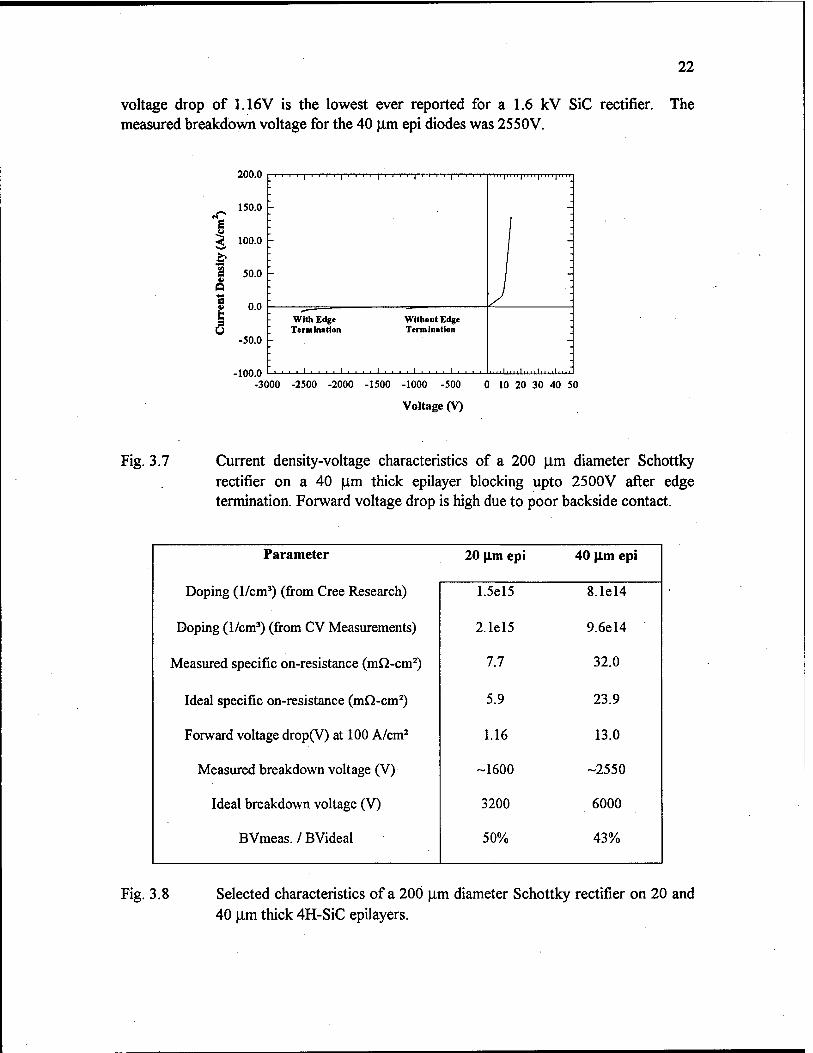
field. Hence, in this experiment, the Schottky diodes were terminated using amorphization of SiC using a blanket Argon implant at 30 keV at a dose of 2xl015 cm"2. The high voltage measurements were done by immersing the diode in a silicone oil. The breakdown voltage of an edge-terminated 20 urn epi (200um diameter) diode (Fig. 3.6) was measured to be >1600V, which was about 2X that of the unterminated diode (-800V). Similarly, the measured breakdown voltage for the 40 (xm epi diodes was >2550V (Fig. 3.7), which was about 2.5X that of the unterminated diode (-1100V). The measured breakdown voltages on the terminated 20 (im and 40 u\m epi diodes were about 50% and 43%, respectively, of the calculated ideal value (Fig. 3.8), indicating that the Argon implant edge termination is not as effective for 3-6 kV diodes on 4H-SiC as it was for the 1 kV diodes, or that the breakdown voltage is reduced by the presence of defects in the epilayers.
S o
fa s U
200.0
150.0
100.0
50.0
0.0
-50.0
-100.0
-150.0
-200.0
_ 1 1 1 1 1 1 1 1 1 1 1 1 1 1 1 1 1 1 1
With Edge Without Edge r Termination Termination
■■ ... i .... i .... i ... .'
~
-2000 -1500 -1000 -500
Voltage (V)
0 12 3 4 5
Fig. 3.6 Current density-voltage characteristics of a 200 urn diameter Schottky rectifier on a 20 urn thick epilayer, exhibiting forward voltage drop of 1.16V at 100 A/cm2 and blocking upto 1600V after edge termination.
3.4 Conclusions
Characteristics of Ni/4H-SiC Schottky rectifiers operating at 1.5 to 2.5 kV, terminated using low energy Ar implants, are reported. At room temperature, an as- deposited Ni/Al 20 |i.m epi (200 \im diameter) Schottky diode exhibited barrier height of 1.7 eV and an ideality factor of 1.07, while the reverse leakage current at 300 K was less than 10"3 A/cm2 at 200V. The forward voltage drop of this diode was only 2.4V at 100 A/cm2. After annealing, this voltage drop reduced to 1.16V at 100 A/cm2. The breakdown voltage was measured to be > 1600V after edge termination. This forward
22
voltage drop of 1.16V is the lowest ever reported for a 1.6 kV SiC rectifier. The measured breakdown voltage for the 40 \im epi diodes was 2550V.
200.0
150.0
I ^ 100.0
3 50.0 Q
E 0.0
-50.0 -
-100.0
l ' ' ' ' I ■ ' ' ' I ' ' ' ' l
With Edge Termination
Without Edge Termination
'l""l""l""l'
■ I ■ ■ ■ ■ I ■ ■.. I ■ ■. ■ I.
-3000 -2500 -2000 -1500 -1000 -500 0 10 20 30 40 50
Voltage (V)
Fig. 3.7 Current density-voltage characteristics of a 200 |im diameter Schottky rectifier on a 40 urn thick epilayer blocking upto 2500V after edge termination. Forward voltage drop is high due to poor backside contact.
Parameter
Doping (1/cm3) (from Cree Research)
20 Jim epi 40 |im epi
1.5el5 8.1el4
Doping (1/cm3) (from CV Measurements) 2.1el5 9.6el4
Measured specific on-resistance (mfl-cm2) 7.7 32.0
Ideal specific on-resistance (mfl-cm2) 5.9 23.9
Forward voltage drop(V) at 100 A/cm2 1.16 13.0
Measured breakdown voltage (V) -1600 -2550
Ideal breakdown voltage (V) 3200 6000
BVmeas. / BVideal 50% 43%
Fig. 3.8 Selected characteristics of a 200 |im diameter Schottky rectifier on 20 and 40 urn thick 4H-SiC epilayers.

23
The measured breakdown voltage in both cases was less than 50% of the ideal, indicating that either the Argon implant edge termination is not as effective for 3-6 kV diodes on 4H-SiC as it was for the 1 kV diodes, or that these thick epilayers contain defects which reduce breakdown voltage. The measured specific on-resistance of 20 \im and 40 u.m epi diodes was -1.5X higher than the calculated drift region resistance over a 0-200 °C temperature range, indicating some contribution from the back contact.
I. B. J. Baliga, "High Voltage Silicon Carbide Devices," in Wide-Bandgap Semiconductors for High Power, High Frequency and High Temperature, Mat. Res. Soc. Symp. Proc, vol. 512, pp. 77-88, 1998.
2 . Q. Wahab et al., "A 3 kV Schottky Barrier Diode in 4H-SiC," Appl. Phys. Lett., vol. 72, pp. 445-447, 1998.
3. D. Alok, R. Raghunathan, and B. J. Baliga, "Planar edge termination for 4H-silicon carbide devices," IEEE Trans. Electron Devices, vol. 43, pp. 1315-1317, 1996.
4. R. Raghunathan and B. J. Baliga, "Temperature Dependence of Hole Impact Ionization Coefficients in 4H and 6H-SiC," Solid State Electronics, vol. 43, pp. 199-211, 1999.
5. D. K. Schroder, Semiconductor Materials and Device Characterization, John Wiley and Sons, New York, 1990.
6. W. Götz, A. Schöner, G. Pensl, W. Suttrop, W. J. Choyke, R. Stein, and S. Leibenzeder, "Nitrogen donors in 4H-silicon carbide," J. Appl. Phys., vol. 73, pp. 3332-3338, 1992.
7. Y. M. Tairov and Y. A. Vodakov, Electroluminiscense, J. I. Pankove, Ed. New York: Springer-Verlag, 1977, pp. 31-61.
8. M. Bhatnagar, B. J. Baliga, H. R. Kirk, and G. A. Rozgonyi, "Effect of Surface Inhomogeneities on the Electrical Characteristics of SiC Schottky Contacts," IEEE Trans. Electron Devices, vol. 43, pp. 150-156, 1996.
9. J. Crofton and S. Sriram, "Reverse Leakage Current Calculations for SiC Schottky Contacts," IEEE Trans. Electron Devices, vol. 43, pp. 2305-2307, 1996.
10. A. Itoh, T. Kimoto, and H. Matsunami, "High Performance of High-Voltage 4H-SiC Schottky Barrier Diodes," IEEE Electron Device Lett., vol. 16, pp. 280-282, 1995.
II. A. Itoh and H. Matsunami, "Analysis of Schottky Barrier Heights of Metal/SiC Contacts and Its Possible Application to High-Voltage Rectifying Devices," Phys. Stat. Sol. (a), vol. 162, pp. 389-408, 1997.
12. B. J. Baliga, "Power semiconductor devices for variable-frequency drives," Proc. IEEE, vol. 82, pp. 1112-1122, 1994.
13. D. Alok and B. J. Baliga, "SiC Device Edge Termination Using Finite Area Argon Implantation," IEEE Trans. Electron Devices, vol. 44, pp. 1013-1017, 1997.
14. A. Itoh, T. Kimoto, and H. Matsunami, "Excellent Reverse Blocking Characteristics of High-Voltage 4H-SiC Schottky Rectifiers with Boron-Implanted Edge Termination," IEEE Electron Device Lett, vol. 17, pp. 139-141, 1996.
15. M. Bhatnagar, P. K. McLarty, and B. J. Baliga, "Silicon-Carbide High-Voltage (400V) Schottky Barrier Diodes," IEEE Electron Device Lett, vol. 13, pp. 501-503, 1992.
25
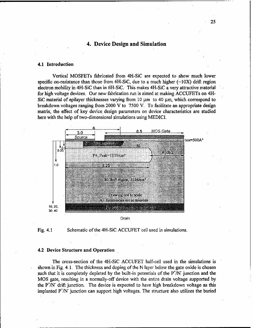
4. Device Design and Simulation
4.1 Introduction
Vertical MOSFETs fabricated from 4H-SiC are expected to show much lower specific on-resistance than those from 6H-SiC, due to a much higher (~10X) drift region electron mobility in 4H-SiC than in 6H-SiC. This makes 4H-SiC a very attractive material for high voltage devices. Our new fabrication run is aimed at making ACCUFETs on 4H- SiC material of epilayer thicknesses varying from 10 u.m to 40 |im, which correspond to breakdown voltages ranging from 2000 V to 7500 V. To facilitate an appropriate design matrix, the effect of key device design parameters on device characteristics are studied here with the help of two-dimensional simulations using MEDICI.
t 10,20, 30,40
. I>awjmg!n$:tO;SSälE:;
:;JM[ÄiS*§iäö$i;är£ißM
tox=500A°
Fig. 4.1 Schematic of the 4H-SiC ACCUFET cell used in simulations.
4.2 Device Structure and Operation
The cross-section of the 4H-SiC ACCUFET half-cell used in the simulations is shown in Fig. 4.1. The thickness and doping of the N layer below the gate oxide is chosen such that it is completely depleted by the built-in potentials of the P+/N" junction and the MOS gate, resulting in a normally-off device with the entire drain voltage supported by the P+/N" drift junction. The device is expected to have high breakdown voltage as this implanted P7N" junction can support high voltages. The structure also utilizes the buried

26
P+ region to suppress the electric field below the gate oxide, thereby preventing oxide rupture. When a positive gate bias is applied, the electrons flow through an accumulation channel created at the SiCVSiC interface. Since the accumulation layer mobility is expected to be higher than the inversion layer mobility, a lower on-resistance is expected for the proposed device.
The epilayer thicknesses were chosen to be 10 u.m, 20 p.m, 30 Jim and 40 |xm. The epilayer (drift region) doping was chosen to be lxlO16 cm"3, 2.1xl015 cm'3, 2.5xl015 cm"3, and 8.4xl014 cm"3, respectively, based on the available starting material. The substrate doping, similarly, was lxlO19 cm*3, 6xl018 cm"3, 7.8xl018 cm"3, and 8.6xl018 cm"3, respectively. The substrate thickness was 2 Jim in all cases. The N+ source was 0.2 p.m deep, and had a gaussian doping profile with a peak concentration of lxl020 cm"3. The buried P+ layer was also chosen to have a gaussian profile with a peak concentration of lxlO19 cm"3 at depth of 0.65 |im. The layer formed a P+/N- junction at a depth of 1 |im,
and chosen to be 16.5 |im wide (Wp). The JFET region width (Wjch), which is the
distance between adjacent buried P+ layers, was varied from 1.5 u.m to 4.5 p.m. The
channel length (Lch) was varied from 1.25 u.m to 4.25 |im. The gate oxide was chosen to be 500 A thick. Both the N+ source and the buried P+ regions were connected to the same electrode and maintained at ground potential during simulations.
"g 3.0e+6
g 2.5e+6 ^ 2.0e+6
1 1.5e+6 u. o 1.0e+6 -
o 5.0e+5 k
Ui 0.0e+0
10 \im epi Nd = 1e16 cm"3
Vd = 2000 V
Wjch varied
1.5 urn 2.5 jim 3.5 urn 4.5 urn
0 1 2 3 4 5 6
Distance from SiC^/SiC interface at center of ACCUFET {\im)
Fig. 4.2 Electric field profile in SiC as a function of the distance of from SiCVSiC interface at the center of the ACCUFET cell for different JFET widths.
4.3 Electric Fields
4.3.1 Effect of JFET width
The JFET region width (Wjch) in the ACCUFET, which is the distance between two adjacent buried P+ layers, is an important design parameter. When a large drain bias
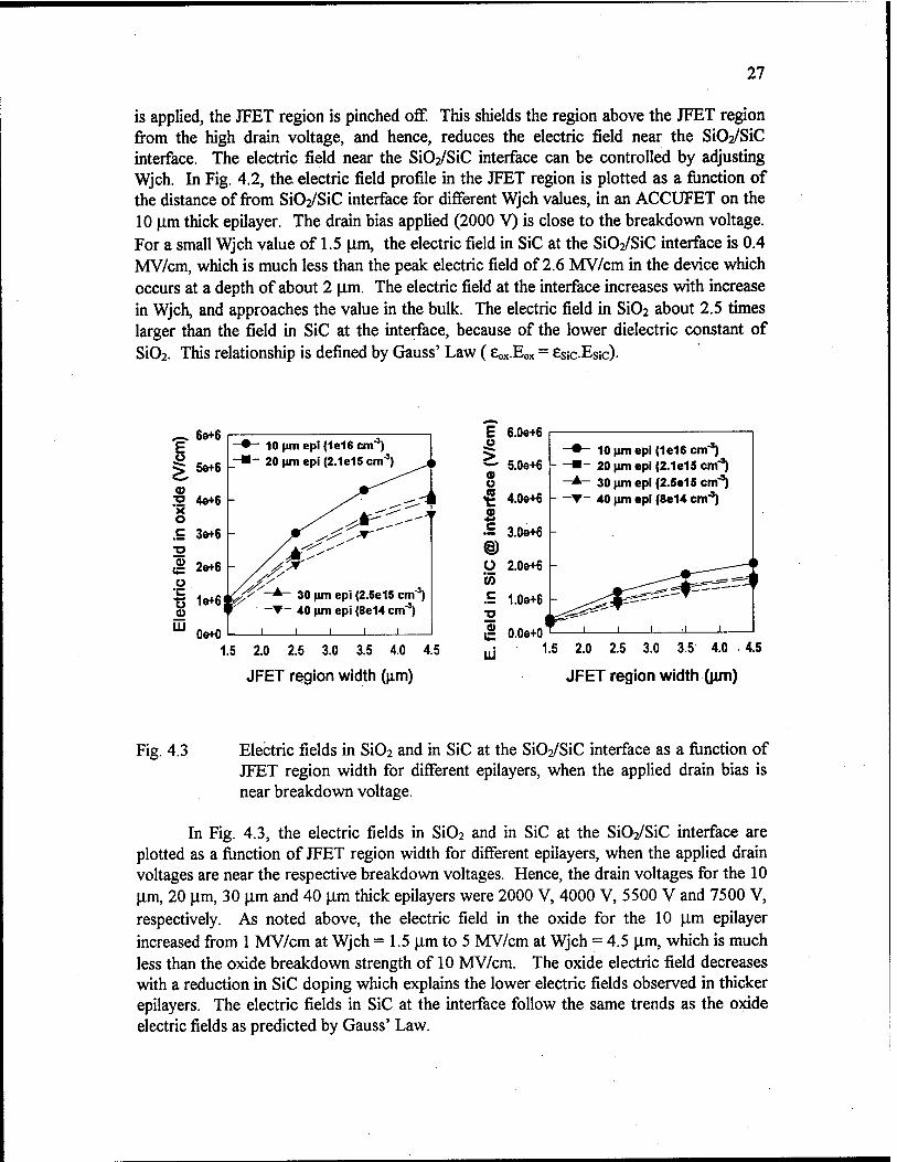
27
is applied, the JFET region is pinched off. This shields the region above the JFET region from the high drain voltage, and hence, reduces the electric field near the SiCVSiC interface. The electric field near the Si02/SiC interface can be controlled by adjusting Wjch. In Fig. 4.2, the electric field profile in the JFET region is plotted as a function of the distance of from Si02/SiC interface for different Wjch values, in an ACCUFET on the 10 pm thick epilayer. The drain bias applied (2000 V) is close to the breakdown voltage. For a small Wjch value of 1.5 |im, the electric field in SiC at the Si02/SiC interface is 0.4 MV/cm, which is much less than the peak electric field of 2.6 MV/cm in the device which occurs at a depth of about 2 urn The electric field at the interface increases with increase in Wjch, and approaches the value in the bulk. The electric field in Si02 about 2.5 times larger than the field in SiC at the interface, because of the lower dielectric constant of Si02. This relationship is defined by Gauss' Law (eox.Eox = eSic.ESic).
.-» 6e+6 E
E 6 Oe+6 —•- 10 jun epi (1e16 cm"3) ,o
S5*6 _""■"" 20 |un epi (2.1e1S cm"3) i 01 Ü
5.0e+6
03 2 4e+6 y^^-i I € 4.0e+6 X o ./ ^^--*
r 0) (2
.£ 3e+6 J* ^^r 3.0e+6 2 £ 2e+6
'S 1»*6! Uyy~~*r~ 30 W* eP' (2.6e16 cm'3) ' -T- 40 \tm epi (8e14 cm"3)
i i i i i
© Ü (5 c
2.0O+6
1.0O+6 03 \ "O
m 0e+0 0) 0.0e+0 1.5 2.0 2.5 3.0 3.5 4.0 4.5
JFET region width (urn) LU
10mnepi (le-löcm"3) 20 Jim epi (2.1 e15 cm"3) 30 urn epi (2.5e1S cm"3) 40 jim epi (8e14 cm"3)
1.5 2.0 2.5 3.0 3.5 4.0 4.5
JFET region width Qim)
Fig. 4.3 Electric fields in Si02 and in SiC at the Si02/SiC interface as a function of JFET region width for different epilayers, when the applied drain bias is near breakdown voltage.
In Fig. 4.3, the electric fields in Si02 and in SiC at the Si02/SiC interface are plotted as a function of JFET region width for different epilayers, when the applied drain voltages are near the respective breakdown voltages. Hence, the drain voltages for the 10 urn, 20 um, 30 um and 40 [im thick epilayers were 2000 V, 4000 V, 5500 V and 7500 V, respectively. As noted above, the electric field in the oxide for the 10 um epilayer increased from 1 MV/cm at Wjch = 1.5 urn to 5 MV/cm at Wjch = 4.5 urn, which is much less than the oxide breakdown strength of 10 MV/cm. The oxide electric field decreases with a reduction in SiC doping which explains the lower electric fields observed in thicker epilayers. The electric fields in SiC at the interface follow the same trends as the oxide electric fields as predicted by Gauss' Law.

28
4.3.2 Trade-off with forward voltage drop
Although reducing Wjch provides the advantage of low oxide electric fields, it comes with a cost. When Wjch is decreased, the cross-sectional area for current flow from the channel into the drift region decreases and this results in an increase in the specific on-resistance of the device. Hence, the forward voltage drop of the device increases with a reduction in Wjch. In Fig. 4.4(a), the forward voltage drop at a current density of 100 A/cm2 is plotted as a function of Wjch for different epilayers, at a gate bias of 5 V. For a Wjch value of 1.5 u,m, the forward voltage drop is about an order of magnitude higher than that for higher values of Wjch. This is because the JFET region is completely pinched off at this low value of Wjch. Further, the forward voltage drop is higher for thicker epilayers. This is due to an increase in the specific on-resistance, caused not only by the increase in epilayer thickness but also by the reduction in the epilayer doping. The trade-off between the electric field in the oxide at device breakdown and the forward voltage drop at 100 A/cm2 at a gate bias of 5 V, presented in Fig. 4.4 (b). It can be seen that for Wjch greater than 3.5 |i.m, the forward voltage does not reduce significantly. Hence, the optimal value of Wjch was chosen to be 3.5 |im, and was used to define a typical cell for subsequent simulations.
§1000.0
1.5 2.0 2.5 3.0 3.5 4.0 4.5
JFET region width (\im)
E .o > 0)
■D "5 o
2 0)
UJ
6e+6
5e+6
4e+6
3e+6
2e+6
1e+6
0e+0 0.1 1.0 10.0 100.0 1000.0
Forward voltage drop at 100 A/cm2 (V)
Vg = 5V <
A . _ f —•— 10 |j.m epi . —■— 20 (im epi
—*- 30 urn epi
- 4 -▼- 40 um epi
- \ XN^
I I I
(a) (b)
Fig. 4.4 (a) Variation of forward voltage drop with JFET region width for different epilayers at a gate bias of 5 V. (b) Trade-off between the electric field in the oxide at device breakdown and the forward voltage drop at 100 A/cm2
at a gate bias of 5 V

29
4.4 Current density-Voltage (J-V) Characteristics
4.4.1 Effect of JFET width
The J-V characteristics of ACCUFETs on the different epilayers at a gate bias of 5 V, for different values of JFET width (Wjch) are presented in Fig. 4.5 and Fig. 4.6. The channel length was assumed to be 2.25 Jim. For each of the epilayers, the J-V curves exhibit a relatively flat saturation region over a large voltage range, with saturation current densities of the order of 300 A/cm2. The breakdown voltage appears to increase slightly with Wjch, which is due to the reduction in the peak electric field in the device with increase in Wjch, as seen in Fig. 4.2. Further, it is observed that the reduction in the peak electric field in the device is accompanied by an increase in the electric field at the SiCVSiC interface. This increase in the electric field near the interface with an increase in Wjch causes a reduction in channel length (channel length modulation). This results in an increase in saturation current at larger values of Wjch (not shown here). The saturation current densities, however, appear to decrease with increasing Wjch because of the increase in the cell width. The slopes of the curves in the linear region increase with increase in Wjch, due to reduction in the specific on-resistance, as discussed in the previous section.
4.4.2 Effect of channel length
The J-V characteristics of ACCUFETs on the different epilayers at a gate bias of 5 V, for different values of channel length (Lch) is presented in Fig. 4.7. Wjch was assumed to be 3.5 urn. For each of the epilayers, the J-V curves exhibit a relatively flat saturation region over a large voltage range. The effects of channel length modulation can be distinctly observed in these curves. It is most apparent among the J-V curves for Lch = 1.25 |im. For this low value of Lch, the saturation current densities decrease with decreasing values of epilayer doping, which is the case with the different materials. Further, the slopes of these curves are much larger than those for the higher values of Lch. The effects of channel length modulation on the saturation current densities and the slopes of the J-V curves in the saturation region, are negligible for Lch > 2.25 urn. The breakdown voltage is independent of the channel length.
4.4.3 Effect of gate bias
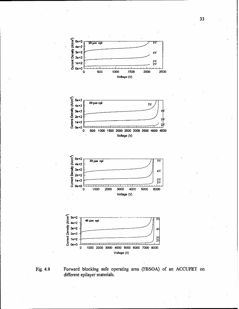
The J-V characteristics of ACCUFETs on the different epilayers for different values of gate bias (Vg) is presented in Fig. 4.8. Wjch and Lch were assumed to be 3.5 Urn and 2.25 |im, respectively. For each of the epilayers, the J-V curves exhibit a relatively flat saturation region over a large drain voltage range. The saturation current densities decrease with decreasing values of epilayer doping, which is the case with the

30
Nd«1e16cm'3
10 Jim epi
2500
500
2. 400
£ 300 « I aoo
Nd ■ 2.1*16 cm" 20 (im «pi
WJch varlad
_i_ j_ _i_
1.6 jun 2.6 Jim 3.6 Jim 4.6 jim
1000 1500 2000 2500 3000 3500 4000 4500
Voltaga (V)
5 Ä«
600
400
300
200
100
0
Nd = 2.5e16cm-' 30 |im
Wjch varied
1.5 jim 2.5 jim 3.5 jim 4.5 |im
1000 2000 3000
Voltage (V)
4000 5000 6000
E 500
§.400 Nd = 8e14 cm-3
40 Jim Wjch varied
_i_
1.5 jim 2.5 jim 3.5 jim 4.5 jim
_i_ j_
1000 2000 3000 4000 5000 6000 7000 8000
Voltage (V)
Fig. 4:5 J-V characteristics of the different epilayers at a gate bias of 5 V exhibiting breakdown voltage dependence on JFET width.

31
Nd = 1e16 crn3
10|imepi Wjch varied
_l_l _LI _L
1.6 um 2.5 (im 3.6 um 4.6 Mm , i .... i ... ,
60 80 100 120 140 160 180 200
Vottage (V)
80 100 120 140 160 180 200
Voltage (V)
80 100 120 140 160 180 200
Voltage (V)
80 100 120 140 160 180 200
Voltage (V)
Fig. 4.6 J-V characteristics of the different epilayer materials at a gate bias of 5 V exhibiting on-resistance dependence on JFET width.

32
& £
ü
lOUU
1200 : 1.25(im 3.25(im 10(imepi I r 2.25 Jim —— 4.25 (im ^^/
800
400
500 1000 1500
Voltage (V)
2000 2500
■£ 1600 o £ 1200 .£ £ B00
■8 ■E 400 S 6 0
1.25 (im ;- 2.25 (im 3.25
4.25 (MI (im
20 lim epi
J
500 1000 1500 2000 2500 3000 3500 4000 4500
Voltage (V)
1000 2000 3000 4000 5000 6000
Voltage (V)
•C 1600
i?- 1200
ü 1000 2000 3000 4000 5000 6000 7000 8000
Voltage (V)
Fig. 4.7 J-V characteristics of the different epilayer materials at a gate bias of 5 V exhibiting breakdown voltage dependence on channel length.
33
1000 1500
Voltage (V)
2500
■ ■ ■ ■ ' ■ ' ' »
500 1000 1500 2000 2500 3000 3500 4000 4500
Voltage (V)
| 5e+2 F
§-4e+2
f" 3e+2 E- <$ 2e+2 %
g 1e+2
o 0e+0
30 \im epi
in ■ ■ i i
1000 2000 3000 4000
Voltage (V)
5V
4V
3V 2V
i ■ .
5000 6000
1000 2000 3000 4000 5000 6000 7000 8000
Voltage (V)
Fig. 4.8 Forward blocking safe operating area (FBSOA) of an ACCUFET on different epilayer materials.

34
different materials, as discussed in the previous section. In all cases, these devices exhibit a square forward blocking safe operating area (FBSOA).
Ln+/2 Source
tP
td
F1S p+
LWjch/2
Wp/2 current spreading. ""
T~* i
ß Hj/fi N- Mi
Wcell/2
Drain
Fig. 4.9 Specific on-resistance components in an ACCUFET.
4.5 Specific On-Resistance
4.5.1 Analytical model
The total specific on-resistance of an ACCUFET has been modeled to be comprised of the N+ source resistance (Rn+), the channel resistance (Rch), the JFET region resistance (Rj), the drift region resistance (Rd) and the substrate resistance (Rsub), as shown in Fig. 4.9. The source specific on-resistance, Rn+, is given by
Rn+ = psn+ . Ln+ . Wcell/2
where, psn+ and Ln+ are the sheet resistance and the length of the source region, respectively, and Wcell is the cell width. The accumulation channel resistance, Rch, is given by
Lch. Wcell Jlna . Cox . (Vg - Vta)
where, Lch is the channel length, [xna is the accumulation channel mobility, Cox is the oxide capacitance, Vg is the gate voltage, and Vta is the accumulation threshold voltage. The JFET region resistance, Rj, is given by

35
RJ tp.Wcdl
q. jut. Nd. b
where tp is the length of the JFBT regten, pn is the c-axis mobility in the JFET region, Nd is the drift region doping, and b it the width of the undepleted JFET region. The values for tp and h were taken from simulations. The drift region resistance, Rd, is given by
Rd Wcell. ln(l + Wp/b)
2, tanp* . q . pa , Nd
(td - Wp/2.tanB)
q . U,D . Nd
where, Wp is the width of the buried P+ layer, and td is the thickness of the drift region which the difference of the epilayer thickness and tp. 6 is the angle of current spreading in the drift region. From simulations, it was observed that the current density in the ACCUFET* is uniformly distributed at thickness greater than 15 urn Based on this observation and from Fig. 4.9, ß is defined to be
ß —[«8* The substrate resistance, Rsub, is given by
Rsub t sub
q. pn_sub. Nd_sub
where, t_sub is the substrate thickness, |in„sub is the c-axis mobility in the substrate, and Nd_sub is the substrate doping
Epi thlcknttt (|im) 10 20 30 40
Epl doping (1/cm3) 1e16 2.1e15 2.5e15 8.4e14
Substrat« thickness (um) 2 2 2 2
Substrat« doping (1/cm3) 1e19 6e18 7.8e18 8.6e18
Channel mobMty (V/cm*.s) 270 260 260 255
Drift mobility (V/cm1.«) 813 891 886 1 913
Substrats mobility (V/cm".s) 73 105 90 80
Threshold voHsoe (V) 1.97 2.21 2.23 2.26
Undepl.JFETwWth,b(um) 2.0 1.3 1.4 0.6
JFET reolon thktk.. tp (um) 1.45 2.1 2.0 2.8
tan(P) 0.66 I °J2 0.71 0.79
Fig. 4.10 Materiel and device parameter» in different starting materials.

36
The important material and device parameters in different starting materials that are required for the calculation of the specific on-resistance components are shown in Fig. 4.10. Using these parameters and the above equations, the individual specific on- resistance components were evaluated for different epilayers as listed in Fig. 4.11. The channel and the drift region resistance are found to contribute significantly to the on- resistance. The contribution from the JFET region becomes significant in the low-doped epilayers. Note that the total specific on-resistance values calculated using the model compare well with those obtained from simulations. Further, for each of the epilayers, the specific on-resistance of the device is compared with the ideal punch-through drift region specific on-resistance. This ratio is of the order of 3X for epilayers of thickness > 20 |im. For the 10 \im epilayer, the ratio is about 9X, primarily due to a large contribution from the channel resistance.
Epi Thickness (urn) 10 20 30 40
R:n+source (mQ.cm2) 0.28 0.28 0.28 0.28
Rxhannel (mQ.cm2) 7.92 8.22 8.22 8.39 R:jfet (mQ.cm2) 0.77 5.14 4.04 26.53 R:drift (mn.cm2) 2.28 14.24 14.71 54.89
R:substrate (mfl.cm2) 1.67e-3 1.98e-3 1.78e-3 1.82e-3
R:total (mQ.cm2) 11.2 27.9 27.2 90 R:total (fromsimulatn.) 7.1 23.6 23.9 98 PunchThru ideal R:drift 0.77 6.7 8.5 32.6 Rrtotal / PT ideal Rdrift 9.2 3.5 2.8 3.0
Fig. 4.11 Specific on-resistance components in different starting materials.
4.5.2 Effect of JFET width
The dependence of specific on-resistance on JFET width (Wjch) in different epilayers is shown in Fig. 4.12. It also shows horizontal straight lines which represent the punch-through ideal drift region specific resistance for each case. For these simulations, the channel length was 2.25 (xm and the gate bias was 5V. The specific on-resistance is observed to reduce rapidly with increase in Wjch, but does not change much for Wjch > 3.5 um.
4.5.3 Effect of channel length
The dependence of specific on-resistance on channel length (Lch) in different epilayers is shown in Fig. 4.13. The JFET width was assumed to be 3.5 fim and the gate

37
bias was 5V. The specific on-resistance increased linearly with increase in Lch. The specific on-resistance for the thicker epilayers is larger because of both lower doping as well as larger thickness.
10000.0 r
cC 1000.0 k-
G , E, 100.0 Q. eo_ c o
OH
2 3 4
JFET Width (Wjch) (urn)
Fig. 4.12 Dependence of specific on-resistance on JFET width in different epilayer materials. The horizontal straight lines indicate the punch-through ideal drift region specific resistance for each case. (Channel length = 2.25 |xm, Gate bias = 5 V)
4.5.4 Effect of gate bias
The dependence of specific on-resistance on gate bias in different epilayers is shown in Fig. 4.14. The JFET width and the channel length were assumed to be 3.5 (xm and 2.25 Urn, respectively. The specific on-resistance decreases with increase in the gate bias. It is observed that the specific on-resistance doesn't reduce much for gate bias values greater than 10 V.

39
5. Conclusion
In the previous chapters, the planar Accumulation-channel Field Effect Transistor (ACCUFET) was introduced and its electrical characteristics on 4H-SiC with different epilayer thicknesses was extensively discussed. This novel planar vertical MOSFET structure, which eliminates both the problems of premature oxide breakdown and low inversion layer mobility (commonly observed in SiC UMOSFETs), was demonstrated at PSRC on both 6H-SiC and 4H-SiC on 10 urn thick epilayers. A room temperature specific on-resistance (Ron,sp) of 18 mQ-cm2 was measured on the best 6H-SiC device at a logic-level gate drive voltage of only 5 V. The measured R^sp for the 6H-SiC ACCUFET was within 2.5X of the measured drift region resistance which was the best value obtained so far for any high voltage SiC MOSFET. Further, the Ron,sp exhibited a positive temperature coefficient which is extremely desirable. In contrast, the room temperature Ro„,,p for the best 4H-SiC device was found to be very high (3.2 Q-cm2 at a gate bias of 5V), but reduced rapidly with increase in temperature to 128 mQ-cm2 at 450 K, due to increase in channel mobility. Simulations had predicted breakdown voltages of over 1500 V for both types of devices. However, the 6H-SiC and 4H-SiC devices had a room- temperature breakdown voltage (BV) of 350V and 450 V, respectively, with a leakage current of < 100 uA. Several test runs and measurements were performed to understand how to improve the specific on-resistance and the breakdown voltage of these devices. The insights thus gained resulted in several changes in the process flow as well as the device design for fabrication of improved high-performance 4H-SiC high voltage ACCUFETs. We plan to fabricate these devices and the results will be given in the next year's report.


![[Chapter I] Basic Knowledge of Discrete Semiconductor Devices...used for high-frequency devices or optical devices. InGaN, the material of blue LED lasers, and SiC and GaN, the materials](https://img.pdfslide.us/doc/110x75/600b8a0d80d15411af0ed397/chapter-i-basic-knowledge-of-discrete-semiconductor-devices-used-for-high-frequency.jpg)


![[Chapter V] Basic Knowledge of Discrete Semiconductor Devices](https://img.pdfslide.us/doc/110x75/616a22fa11a7b741a34f32ba/chapter-v-basic-knowledge-of-discrete-semiconductor-devices.jpg)