Embed Size (px)
Citation preview
Freescale Semiconductor, Inc.User’s Guide
© Freescale Semiconductor, Inc., 2015. All rights reserved.
Document Number: KT33909UGRev. 1.0, 4/2015
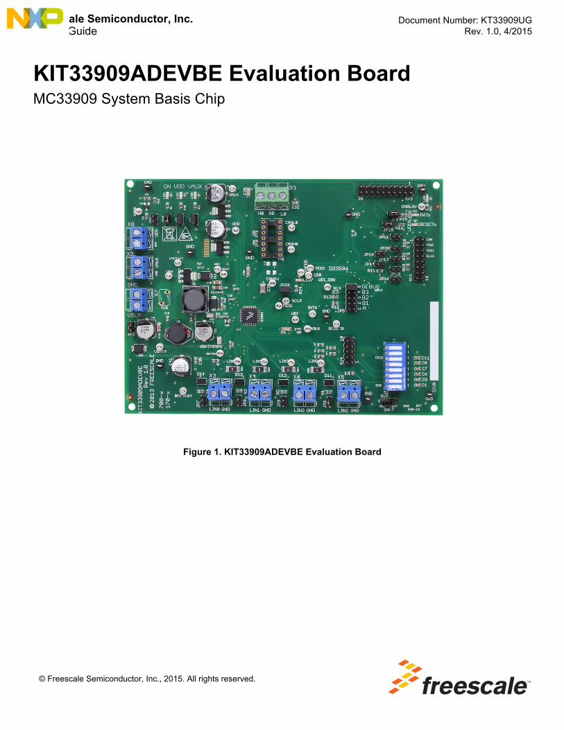
KIT33909ADEVBE Evaluation BoardMC33909 System Basis Chip
Figure 1. KIT33909ADEVBE Evaluation Board
KT33909UG Rev. 1.02 Freescale Semiconductor, Inc.
Contents
1 Important Notice . . . . . . . . . . . . . . . . . . . . . . . . . . . . . . . . . . . . . . . . . . . . . . . . . . . . . . . . . . . . . . . . . . . . . . . . . . . . . . . . . . . . . . . . . . . 32 Getting Started . . . . . . . . . . . . . . . . . . . . . . . . . . . . . . . . . . . . . . . . . . . . . . . . . . . . . . . . . . . . . . . . . . . . . . . . . . . . . . . . . . . . . . . . . . . . 43 Getting to Know the Hardware . . . . . . . . . . . . . . . . . . . . . . . . . . . . . . . . . . . . . . . . . . . . . . . . . . . . . . . . . . . . . . . . . . . . . . . . . . . . . . . . 54 Accessory Interface Board . . . . . . . . . . . . . . . . . . . . . . . . . . . . . . . . . . . . . . . . . . . . . . . . . . . . . . . . . . . . . . . . . . . . . . . . . . . . . . . . . . 155 Installing the Software and Setting up the Hardware . . . . . . . . . . . . . . . . . . . . . . . . . . . . . . . . . . . . . . . . . . . . . . . . . . . . . . . . . . . . . . 166 Schematic . . . . . . . . . . . . . . . . . . . . . . . . . . . . . . . . . . . . . . . . . . . . . . . . . . . . . . . . . . . . . . . . . . . . . . . . . . . . . . . . . . . . . . . . . . . . . . . 237 Board Layout. . . . . . . . . . . . . . . . . . . . . . . . . . . . . . . . . . . . . . . . . . . . . . . . . . . . . . . . . . . . . . . . . . . . . . . . . . . . . . . . . . . . . . . . . . . . . 248 Board Bill of Materials . . . . . . . . . . . . . . . . . . . . . . . . . . . . . . . . . . . . . . . . . . . . . . . . . . . . . . . . . . . . . . . . . . . . . . . . . . . . . . . . . . . . . . 259 Accessory Item Bill of Materials . . . . . . . . . . . . . . . . . . . . . . . . . . . . . . . . . . . . . . . . . . . . . . . . . . . . . . . . . . . . . . . . . . . . . . . . . . . . . . 2710 References . . . . . . . . . . . . . . . . . . . . . . . . . . . . . . . . . . . . . . . . . . . . . . . . . . . . . . . . . . . . . . . . . . . . . . . . . . . . . . . . . . . . . . . . . . . . . 2811 Revision History . . . . . . . . . . . . . . . . . . . . . . . . . . . . . . . . . . . . . . . . . . . . . . . . . . . . . . . . . . . . . . . . . . . . . . . . . . . . . . . . . . . . . . . . . 29

Important Notice
KT33909UG Rev. 1.0 Freescale Semiconductor, Inc. 3
1 Important NoticeFreescale provides the enclosed product(s) under the following conditions:
This evaluation kit is intended for use of ENGINEERING DEVELOPMENT OR EVALUATION PURPOSES ONLY. It is provided as a sample IC pre-soldered to a printed circuit board to make it easier to access inputs, outputs, and supply terminals. This evaluation board may be used with any development system or other source of I/O signals by simply connecting it to the host MCU or computer board via off-the-shelf cables. This evaluation board is not a Reference Design and is not intended to represent a final design recommendation for any particular application. Final device in an application will be heavily dependent on proper printed circuit board layout and heat sinking design as well as attention to supply filtering, transient suppression, and I/O signal quality.
The goods provided may not be complete in terms of required design, marketing, and or manufacturing related protective considerations, including product safety measures typically found in the end product incorporating the goods. Due to the open construction of the product, it is the user's responsibility to take any and all appropriate precautions with regard to electrostatic discharge. In order to minimize risks associated with the customers applications, adequate design and operating safeguards must be provided by the customer to minimize inherent or procedural hazards. For any safety concerns, contact Freescale sales and technical support services.
Should this evaluation kit not meet the specifications indicated in the kit, it may be returned within 30 days from the date of delivery and will be replaced by a new kit.
Freescale reserves the right to make changes without further notice to any products herein. Freescale makes no warranty, representation or guarantee regarding the suitability of its products for any particular purpose, nor does Freescale assume any liability arising out of the application or use of any product or circuit, and specifically disclaims any and all liability, including without limitation consequential or incidental damages. “Typical” parameters can and do vary in different applications and actual performance may vary over time. All operating parameters, including “Typical”, must be validated for each customer application by customer’s technical experts.
Freescale does not convey any license under its patent rights nor the rights of others. Freescale products are not designed, intended, or authorized for use as components in systems intended for surgical implant into the body, or other applications intended to support or sustain life, or for any other application in which the failure of the Freescale product could create a situation where personal injury or death may occur.
Should the Buyer purchase or use Freescale products for any such unintended or unauthorized application, the Buyer shall indemnify and hold Freescale and its officers, employees, subsidiaries, affiliates, and distributors harmless against all claims, costs, damages, and expenses, and reasonable attorney fees arising out of, directly or indirectly, any claim of personal injury or death associated with such unintended or unauthorized use, even if such claim alleges Freescale was negligent regarding the design or manufacture of the part.Freescale™ and the Freescale logo are trademarks of Freescale Semiconductor, Inc. All other product or service names are the property of their respective owners. © Freescale Semiconductor, Inc. 2015

Getting Started
KT33909UG Rev. 1.04 Freescale Semiconductor, Inc.
2 Getting Started
2.1 Kit Contents/Packing ListThe KIT33909ADEVBE contents include:
• Assembled and tested evaluation board/module in anti-static bag.• Quick Start Guide, Analog Tools• Warranty card
2.2 Jump StartFreescale's analog product development boards help to easily evaluate Freescale products. These tools support analog mixed signal and power solutions including monolithic ICs using proven high-volume SMARTMOS mixed signal technology, and system-in-package devices utilizing power, SMARTMOS and MCU dies. Freescale products enable longer battery life, smaller form factor, component count reduction, ease of design, lower system cost and improved performance in powering state of the art systems.
• Go to www.freescale.com/analogtools• Locate your kit• Review your Tool Summary Page• Look for
• Download documents, software and other informationOnce the files are downloaded, review the user guide in the bundle. The user guide includes setup instructions, BOM and schematics. Jump start bundles are available on each tool summary page with the most relevant and current information. The information includes everything needed for design.
2.3 Required Equipment and Software To use this kit, you need:
• Power supply: 2.7 to 36 V with current limit set initially to 2.0 A
• Oscilloscope (preferably 4-channel)
• Function Generator/MCU to toggle TXD pins of CAN 0 and LIN0-4
• SPIgen Software with KITUSBSPIDGLVME: http://www.freescale.com/spigen
• Voltage meter to monitor various voltage levels
2.4 System RequirementsThe kit requires the following to function properly with the software:
• Windows® XP, Windows 7, or Vista in 32-bit and 64-bit versions
Jump Start Your Design
Getting to Know the Hardware
KT33909UG Rev. 1.0 Freescale Semiconductor, Inc. 5
3 Getting to Know the Hardware
3.1 Board OverviewThe KIT33909ADEVBE Evaluation Board (EVB) is an easy-to-use circuit board allowing the user to exercise all the functions of the MC33909 system basis chip. A PC communicates to the EVB through a USB/SPI dongle (KITUSBSPIDGLEVME) connected to the PC's USB port. The Freescale SPIGen (version 7.0 and above) program provides the user interface to the MC33909 SPI port and allows the user to validate the capabilities of the IC, send commands to the IC, and receive status information from the IC.
3.2 Board FeaturesThe board features are as follows:
• Supports all regulated voltages - VPRE, VDD, VAUX and CAN5V.
• Provides access to the CAN0 (ISO11898-2 and -5) physical layer.
• Provides configurable terminations for CAN0 via 12 pin DIP socket.
• Offers access to the LIN0-4 (LIN 2.1 and SAE J2602-2) physical layers.
• Provides selectable Safe Mode resistors and a Watchdog Inhibit mode.
• Offers MCU monitoring and fail-safe support
• Provides a USB-to-SPI dongle interface
3.3 Device FeaturesThis evaluation board features the following Freescale product:
Table 1. Features
Device Description Features
MC33909System Basis Chip with DC/DC and Multiple Switch-to-Ground Interface
• VDD rail (3.3 V or 5.0 V) operates down to 2.7 V on VBATP (provided by VPRE Buck/Boost)
• VAUX rail (3.3 V or 5.0 V) capable of surviving short-to-battery (40 V) condi-tions
• Low Q current operation for low-power sleep mode, typ. 125 A
• Secured SPI and advanced watchdog
• Advanced power management unit for the MCU and additional integrated cir-cuits
• Highly flexible SMPS pre-regulator, allowing two topologies: non-inverting buck-boost or standard buck
Getting to Know the Hardware
KT33909UG Rev. 1.06 Freescale Semiconductor, Inc.
3.4 Board Description This EVB consists of an MC33909 system basis chip and power conditioning circuitry. The board provides access to the IC for functional testing, and offers compatible connectivity with external circuits.
Figure 2. KIT33909ADEVBE
VDD
VAUX
BATTERYCONNECTION
PI FILTER
ON, VDD, andVAUX LED's
VAUX and VDDPNP's
CAN BUS andTERMINATION SOCKET
20 PIN SV3 CONNECTORIC SIGNALS
SPI DONGLELED
INTb andRESETbLED's
SPI DONGLECONNECTOR
SAFE MODE
SGx SWITCHES andCONNECTOR
LIN 0-4 with OPTIONAL 1Kohm PULL-UP to BATTERY
VPRESMPS
Getting to Know the Hardware
KT33909UG Rev. 1.0 Freescale Semiconductor, Inc. 7
3.5 LED DisplayThe following LEDs are provided as visual output devices for the KIT33909ADEVBE evaluation board:
Figure 3. LED Locations on the KIT33909ADEVBE Evaluation Board
1. LED No 1—ON Indicates when JP3 is on and Battery is supplied
2. LED No 2—INTb Indicates that the INTb pin has been activated low
3. LED No 3—RESETb Indicates that the RESETb pin has been activated low
4. LED No 4—VDD Indicates that the VDD supply is operating
5. LED No 5—VAUX Indicates that the VAUX supply is operating
6. LED No 6 Indicates SPI Dongle is powered and connected correctly to the 33909 board
7. LED No 7—SAFEb Indicates that the SAFE mode has been entered
ON (LED1)
VDD (LED4)
VAUX (LED5)
INTb (LED2) RESETb (LED3)
LED6
SAFEb (LED7)
Getting to Know the Hardware
KT33909UG Rev. 1.08 Freescale Semiconductor, Inc.
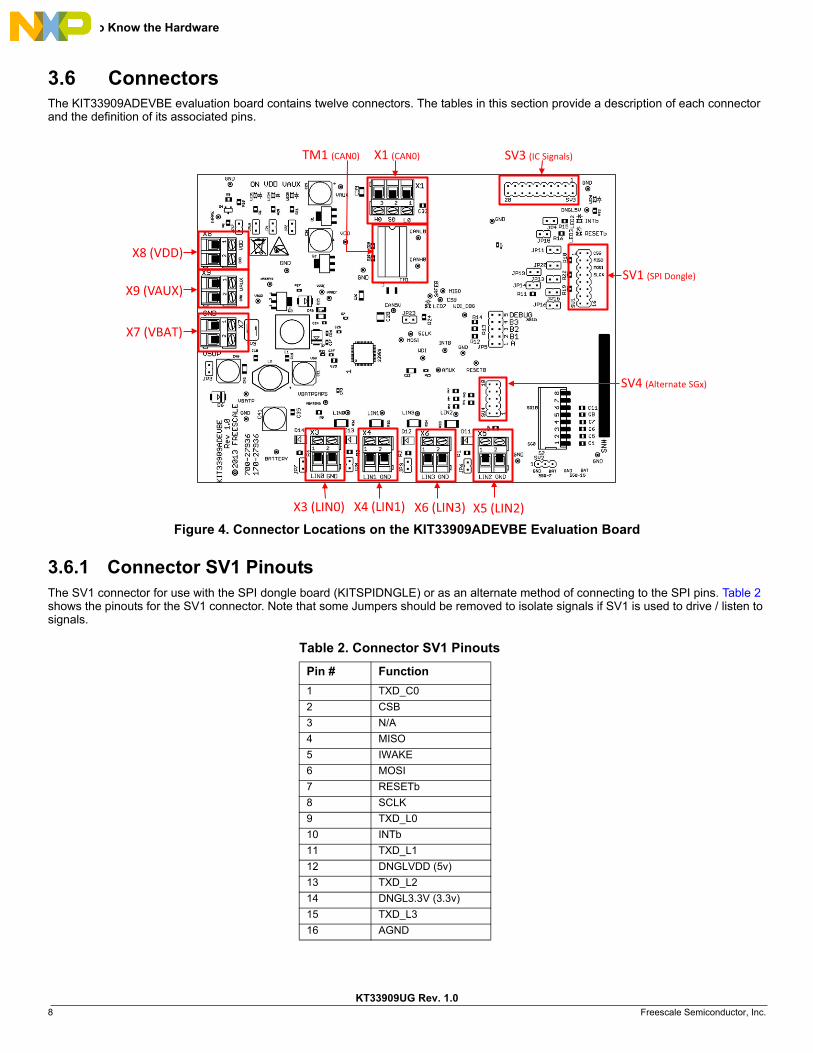
3.6 ConnectorsThe KIT33909ADEVBE evaluation board contains twelve connectors. The tables in this section provide a description of each connector and the definition of its associated pins.
Figure 4. Connector Locations on the KIT33909ADEVBE Evaluation Board
3.6.1 Connector SV1 PinoutsThe SV1 connector for use with the SPI dongle board (KITSPIDNGLE) or as an alternate method of connecting to the SPI pins. Table 2 shows the pinouts for the SV1 connector. Note that some Jumpers should be removed to isolate signals if SV1 is used to drive / listen to signals.
Table 2. Connector SV1 Pinouts
Pin # Function
1 TXD_C0
2 CSB
3 N/A
4 MISO
5 IWAKE
6 MOSI
7 RESETb
8 SCLK
9 TXD_L0
10 INTb
11 TXD_L1
12 DNGLVDD (5v)
13 TXD_L2
14 DNGL3.3V (3.3v)
15 TXD_L3
16 AGND
SV1 (SPI Dongle)
SV3 (IC Signals) X1 (CAN0)
SV4 (Alternate SGx)
TM1 (CAN0)
X3 (LIN0) X4 (LIN1) X6 (LIN3) X5 (LIN2)
X8 (VDD)
X9 (VAUX)
X7 (VBAT)
Getting to Know the Hardware
KT33909UG Rev. 1.0 Freescale Semiconductor, Inc. 9
3.6.2 Connector SV3 PinoutsThe SV3 Connector provides IC usage off of the EVB.
3.6.3 Connector SV4 PinoutsConnector SV4 is an alternate connector for SGx pins for use off of the EVB.
Table 3. Connector SV3 Pinouts
Pin # Function
1 TXD_L0
2 RXD_L0
3 TXD_L1
4 RXD_L1
5 TXD_L2
6 RXD_L2
7 TXD_L3
8 RXD_L3
9 TXD_C0
10 N/A
11 RXD_C0
12 N/A
13 RESETb
14 INTb
15 SAFEb
16 AMUX
17 VDD
18 VAUX
19 AGND
20 AGND
Table 4. Connector SV4 Pinouts
Pin # Function
1 SG0
2 SG1
3 SG2
4 SG3
5 SG4
6 SG5
7 AGND
8 N/A
9 N/A
10 Battery
Getting to Know the Hardware
KT33909UG Rev. 1.010 Freescale Semiconductor, Inc.
3.6.4 Connector X1 (CAN0) PinoutsConnector X1(CAN0) provides a link to the CAN0 Bus.
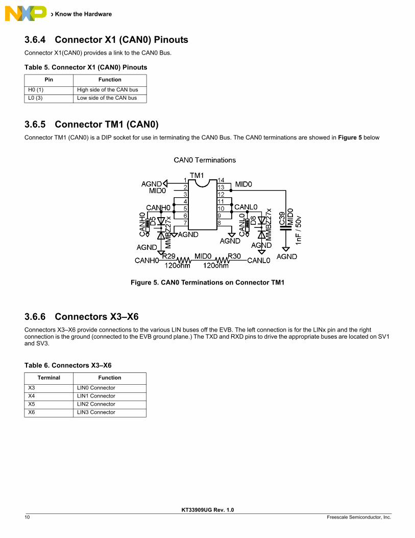
3.6.5 Connector TM1 (CAN0)Connector TM1 (CAN0) is a DIP socket for use in terminating the CAN0 Bus. The CAN0 terminations are showed in Figure 5 below
Figure 5. CAN0 Terminations on Connector TM1
3.6.6 Connectors X3–X6Connectors X3–X6 provide connections to the various LIN buses off the EVB. The left connection is for the LINx pin and the right connection is the ground (connected to the EVB ground plane.) The TXD and RXD pins to drive the appropriate buses are located on SV1 and SV3.
Table 5. Connector X1 (CAN0) Pinouts
Pin Function
H0 (1) High side of the CAN bus
L0 (3) Low side of the CAN bus
Table 6. Connectors X3–X6
Terminal Function
X3 LIN0 Connector
X4 LIN1 Connector
X5 LIN2 Connector
X6 LIN3 Connector
Getting to Know the Hardware
KT33909UG Rev. 1.0 Freescale Semiconductor, Inc. 11
3.6.7 Connectors X8 and X9 (Regulators)Connectors X8 and X9 provide linkage to VDD and VAUX externally.
3.7 Test Point DefinitionsThe following test-point jumpers provide access to signals on the MC33909 IC:
Table 7. Connectors X8 and X9
Terminal Function
X8 VDD Connector
X9 VAUX Connector
Table 8. MC33909 Test Point Definitions
Schematic Label Name Description
BATTERY BATTERY Supply Voltage for EVB
VBATP VBATP VBATP Supply Voltage
VBATSMPS VBATSMPS VBATSMPS Supply Voltage
VBATSNS VBATSNS VBATSNS Supply Voltage
VSW2 VSW2 Switching Regulator Output
VPREGATE VPREGATE Gate Control of Low Side FET
VPRE VPRE Pre-Regulator Voltage/Supply for VDD/VAUX/CAN5V
VPREF VPREF Secondary Test Point for Pre-Regulator Voltage
VDD VDD VDD Supply Voltage
VAUX VAUX Auxiliary Supply Voltage
IWAKE IWAKE Wake-up from SPI on VDD
CANL0 CANL0 CAN Low Output
CANH0 CANH0 CAN High Output
CAN5V CAN5V CAN Interface Output Voltage
MISO MISO Serial Output to the MCU/SPIGEN
MOSI MOSI SPI Control Data Input
CSB CSB SPI Control Chip Select Bar Input
SCLK SCLK SPI Control Clock Input
DNGL5V DNGL5V SPI Dongle Supply Voltage
WDI WDI Watchdog Inhibit
WDI DEBUG WDI DEBUG Watchdog Debug Mode (Set to 12 V to disable Watchdog)
SAFEB SAFEB Safe Circuitry Output
INTB INTB Input Change of State Detection Output
AMUX AMUX Analog Multiplex Output
RESETB RESETB Device Reset Output
LIN0 LIN0 LIN0 Bus Connection
LIN1 LIN1 LIN1 Bus Connection
LIN2 LIN2 LIN2 Bus Connection
LIN3 LIN3 LIN3 Bus Connection
GND GND Ground Plane Connection
Getting to Know the Hardware
KT33909UG Rev. 1.012 Freescale Semiconductor, Inc.
3.8 USB/SPI Dongle ConnectorUSB/SPI dongle connector mates with the 16 conductor flat cable connecting to the USB/SPI Dongle (KITUSBSPIDGLEVME).This is a 16 pin, 0.1” center, dual-row connector designed to interface directly to the USB/SPI Dongle unit. The USB/SPI dongle connector consists of the following 16 pins.
Table 9. USB/SPI Dongle Connector Pinouts
Pin Number Name Description
1 CSB SPI signal, Chip Select Bar
2 CNTL2 CNTL2 connected to TXD_C0
3 SO SPI signal, Serial Out
4 CNTL1 CNTL1 connected to TXD_C1
5 SI SPI signal, Serial In
6 CNTL0 CNTL0 connected to IWAKE
7 SCLK SPI signal, Serial Clock
8 DATA4 DATA4 connected to RESETB
9 CNTL3 CNTL3 connected to INTB
10 DATA3 DATA3 Connected to TXD_L0
11 VDD +5.0 V VDD from USB
12 DATA2 DATA2 connected to TXD_L2
13 +3.3V +3.3 V from USB (Not Used)
14 DATA1 DATA1 Connected to TXD_L2
15 GND Signal Ground
16 DATA0 DATA0 connected to TXD_L3

Getting to Know the Hardware
KT33909UG Rev. 1.0 Freescale Semiconductor, Inc. 13
3.9 Jumper DefinitionsThe following table defines the evaluation board jumper positions and explains their functions. (The default settings are shown in bold.)
Figure 6. Jumper locations on the KIT33909ADEVBE evaluation board
Table 10. KIT33909ADEVBE Evaluation Board Jumper Definitions
Jumper Description Setting Connection
SV2SG0 - 5 selection for closing switch to Battery or Ground (only one jumper should be set)
1-2 Switch to Ground
2-3 Switch to Battery
JP1 VDD LED IN / OUT Enables LED indicating VDD voltage
JP2 VAUX LED IN / OUT Enables LED indicating VAUX voltage
JP3 EVB VSUP IN / OUT Applies VSUP to main board
JP4 INTB LED IN / OUT Provides the INTb LED a pull up path to VDD
JP5 SAFE Mode Selection IN / OUT
A single jumper should be used to select one of the following modes (SAFE mode A, B1, B2, B3 or DEBUG). When selecting DEBUG the user shall apply 12 V to the WDI_DBG test point before pow-ering the IC
JP6 LIN2 Bus IN / OUTConnects LIN2 to battery through 1 kohm resistor and diode
JP7 LIN0 Bus IN / OUTConnects LIN0 to battery through 1 kohm resistor and diode
JP8 LIN1 Bus IN / OUTConnects LIN1 to battery through 1 kohm resistor and diode
JP9 LIN3 Bus IN / OUTConnects LIN3 to battery through 1 kohm resistor and diode
Getting to Know the Hardware
KT33909UG Rev. 1.014 Freescale Semiconductor, Inc.
3.10 SwitchesThe KIT33909ADEVBE contains one block of switches (S2) that allows easy testing of the SGx functionality. The Jumper JP1 is used to determine the connection on a close of the switch, either Battery (BAT) or Ground (GND). S2 provides: SG0–5 selections for closing switch to Battery or Ground (only one jumper should be set). The allocation is as follows:
JP10 ON LED IN / OUT Enables LED indicating EVB is powered on
JP11 TXD_C0 Connection IN / OUT Connects TXD_C0 to SPI Dongle
JP13 TXD_L0 Connection IN / OUT Connects TXD_L0 to SPI Dongle
JP14 TXD_L1 Connection IN / OUT Connects TXD_L1 to SPI Dongle
JP15 TXD_L2 Connection IN / OUT Connects TXD_L2 to SPI Dongle
JP16 TXD_L3 Connection IN / OUT Connects TXD_L3 to SPI Dongle
JP17 IWAKE Signal IN / OUTApplies IWAKE signal from SPI dongle to IWAKE circuit
JP18 RESETB LED IN / OUT Provides the RESETb LED a pull up path to VDD
JP19 INTB Connection IN / OUT Connects INTb to SPI Dongle
JP20 RESETB Connection IN / OUT Connects RESETb to SPI Dongle
JP23 SAFEB Pull-Up IN / OUT Provides SAFEb pull up to Battery
Table 11. KIT33909ADEVBE Switches
S2 Position SGx Connection
1 SG0
2 SG1
3 SG2
4 SG3
5 SG4
6 SG5
Table 10. KIT33909ADEVBE Evaluation Board Jumper Definitions
Jumper Description Setting Connection
Accessory Interface Board
KT33909UG Rev. 1.0 Freescale Semiconductor, Inc. 15
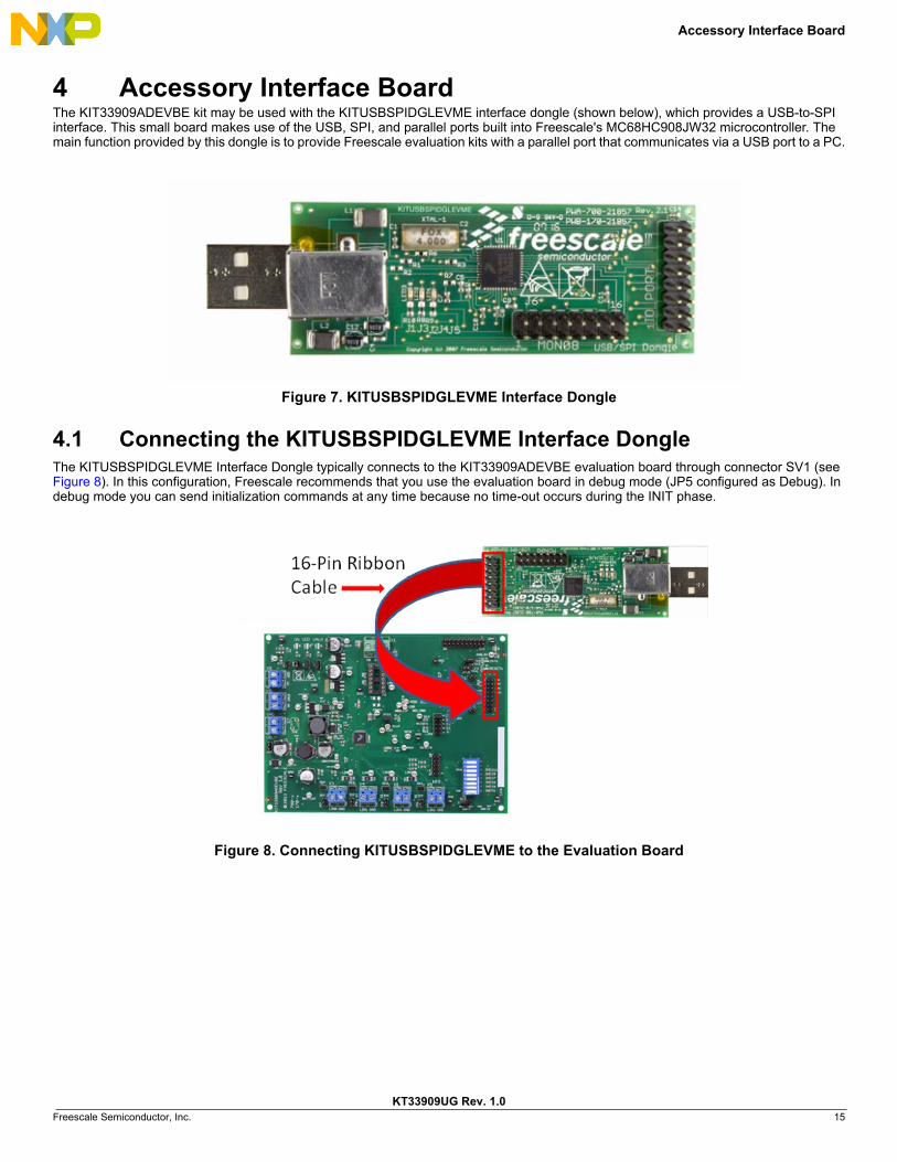
4 Accessory Interface BoardThe KIT33909ADEVBE kit may be used with the KITUSBSPIDGLEVME interface dongle (shown below), which provides a USB-to-SPI interface. This small board makes use of the USB, SPI, and parallel ports built into Freescale's MC68HC908JW32 microcontroller. The main function provided by this dongle is to provide Freescale evaluation kits with a parallel port that communicates via a USB port to a PC.
Figure 7. KITUSBSPIDGLEVME Interface Dongle
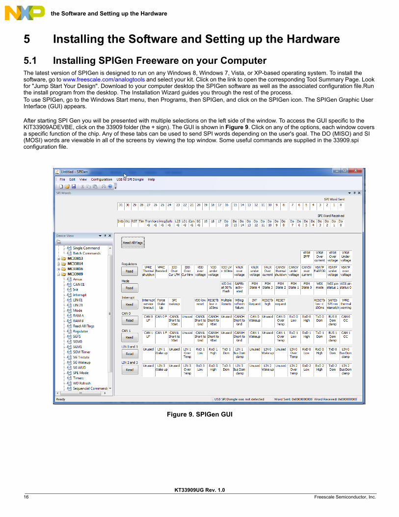
4.1 Connecting the KITUSBSPIDGLEVME Interface DongleThe KITUSBSPIDGLEVME Interface Dongle typically connects to the KIT33909ADEVBE evaluation board through connector SV1 (see Figure 8). In this configuration, Freescale recommends that you use the evaluation board in debug mode (JP5 configured as Debug). In debug mode you can send initialization commands at any time because no time-out occurs during the INIT phase.
Figure 8. Connecting KITUSBSPIDGLEVME to the Evaluation Board
Installing the Software and Setting up the Hardware
KT33909UG Rev. 1.016 Freescale Semiconductor, Inc.
5 Installing the Software and Setting up the Hardware
5.1 Installing SPIGen Freeware on your Computer The latest version of SPIGen is designed to run on any Windows 8, Windows 7, Vista, or XP-based operating system. To install the software, go to www.freescale.com/analogtools and select your kit. Click on the link to open the corresponding Tool Summary Page. Look for "Jump Start Your Design". Download to your computer desktop the SPIGen software as well as the associated configuration file.Run the install program from the desktop. The Installation Wizard guides you through the rest of the process.To use SPIGen, go to the Windows Start menu, then Programs, then SPIGen, and click on the SPIGen icon. The SPIGen Graphic User Interface (GUI) appears.
After starting SPI Gen you will be presented with multiple selections on the left side of the window. To access the GUI specific to the KIT33909ADEVBE, click on the 33909 folder (the + sign). The GUI is shown in Figure 9. Click on any of the options, each window covers a specific function of the chip. Any of these tabs can be used to send SPI words depending on the user's goal. The DO (MISO) and SI (MOSI) words are viewable in all of the screens by viewing the top window. Some useful commands are supplied in the 33909.spi configuration file.
Figure 9. SPIGen GUI
Installing the Software and Setting up the Hardware
KT33909UG Rev. 1.0 Freescale Semiconductor, Inc. 17
5.2 Describing the GUI InterfaceThe Graphical User Interface allows the user to program all SPI features by using a friendly interface as well as modifying the register table manually for advance users. The MC33909 Tab allows for much easier usage as the user does not have to know the address or command bits to do an action, the program will take care of this.
5.3 Using SPIGenBefore using the SPIGen program features, you should have the appropriate MC33909 datasheet available. The datasheet provides detailed information on device features and flag settings.
In general, SPIGen provides three ways of setting and resetting MC33909 register bits
1. Within each sub-tab, click on the bits directly in the Selected register (white color changes to blue color if 1 is selected) and hit the "Write" button. The corresponding received word will be displayed in the 32 bit "SPi Word Received" section at the top of the screen. In addition, you can also read the specific bits for the selected register by hitting the "Read" button.
2. Use one of the pre-defined buttons in the selection field. It will highlight the correct bits and the user can send the command by hitting the 'Write" button.
3. Directly address the register and send the desired SPI word using 32-bit "SPI Word Sent option" at the top of the interface.
Note that the write button will send what is adjusted.The read button will set the boxes to the current IC state.
The following sections provide details on three of the most commonly used tab options.
Installing the Software and Setting up the Hardware
KT33909UG Rev. 1.018 Freescale Semiconductor, Inc.
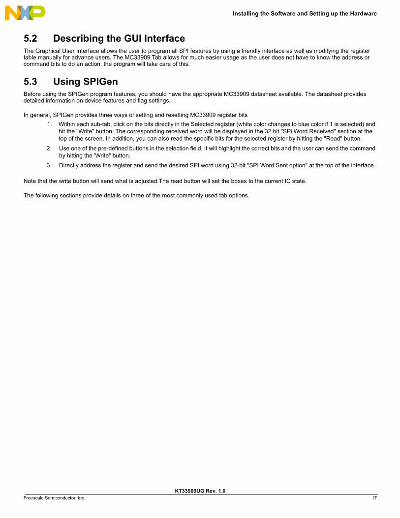
5.3.0.1 The W/D Refresh Tab
In general, access the “W/D Refresh” tab first when the device is in Debug mode (the Safe Jumper J5 is set and the WDI_Debug Test Point is connected to 12 V.). In this tab, selecting "Send simple refresh" will put the device into Normal mode. Normal mode gives you read/write access to all registers except for those which require the device to be in an Init state.
Figure 10. The W/D Refresh Tab
Installing the Software and Setting up the Hardware
KT33909UG Rev. 1.0 Freescale Semiconductor, Inc. 19
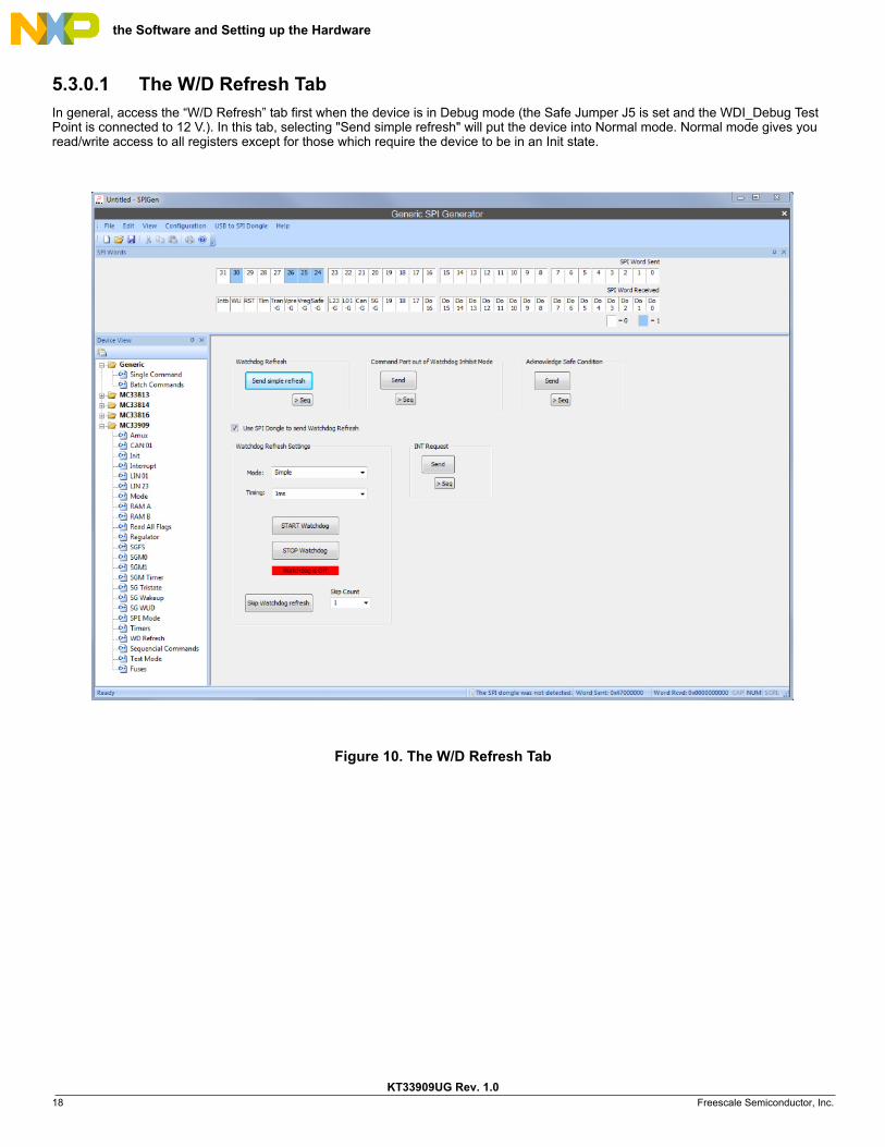
5.3.0.2 The Regulator Tab
The "Regulator" tab allows you to enable/disable the VAUX and CAN5V regulators. (The CAN5V regulator must be on to enable LIN bus operation.) The Regulator Tab also allows you to read all the regulator flags. The flags provide the current status (e.g. VBATP batfail = 1 after POR, Vpre Boosted = 1 since the IC starts at VBATP = 5.0 V which is in the boost range) of each of the regulators. Reading the regulator tabs will reset the register contents to zero (clear all flags.) If an error is pending for any flag, that flag will continue to reset to 1 each time a Read is executed. You must clear the associated fault before resuming normal Read operations on the flag.
Notice that all adjustments done to VAUX or VDD will be valid only after you press the write button.
Figure 11. The Regulator Tab
Installing the Software and Setting up the Hardware
KT33909UG Rev. 1.020 Freescale Semiconductor, Inc.
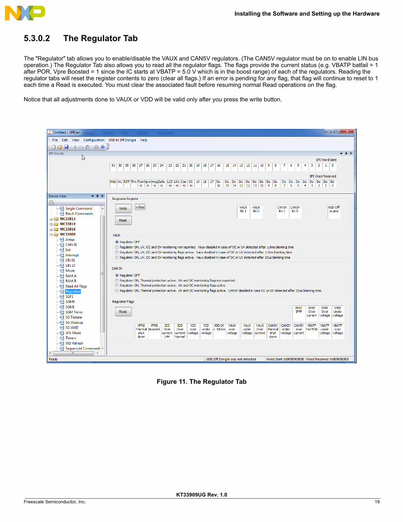
5.3.0.3 The Sequential Commands Tab
The "Sequential Commands" tab allows you to build a set of commands and subsequently send those commands to the “Sequence” tab. (To do so, hit the >seq button by the desired SPI word.) You can also rearrange the order of commands, add wait statements, and loop a sequence of commands.
Figure 12. The Sequential Commands Tab
Installing the Software and Setting up the Hardware
KT33909UG Rev. 1.0 Freescale Semiconductor, Inc. 21
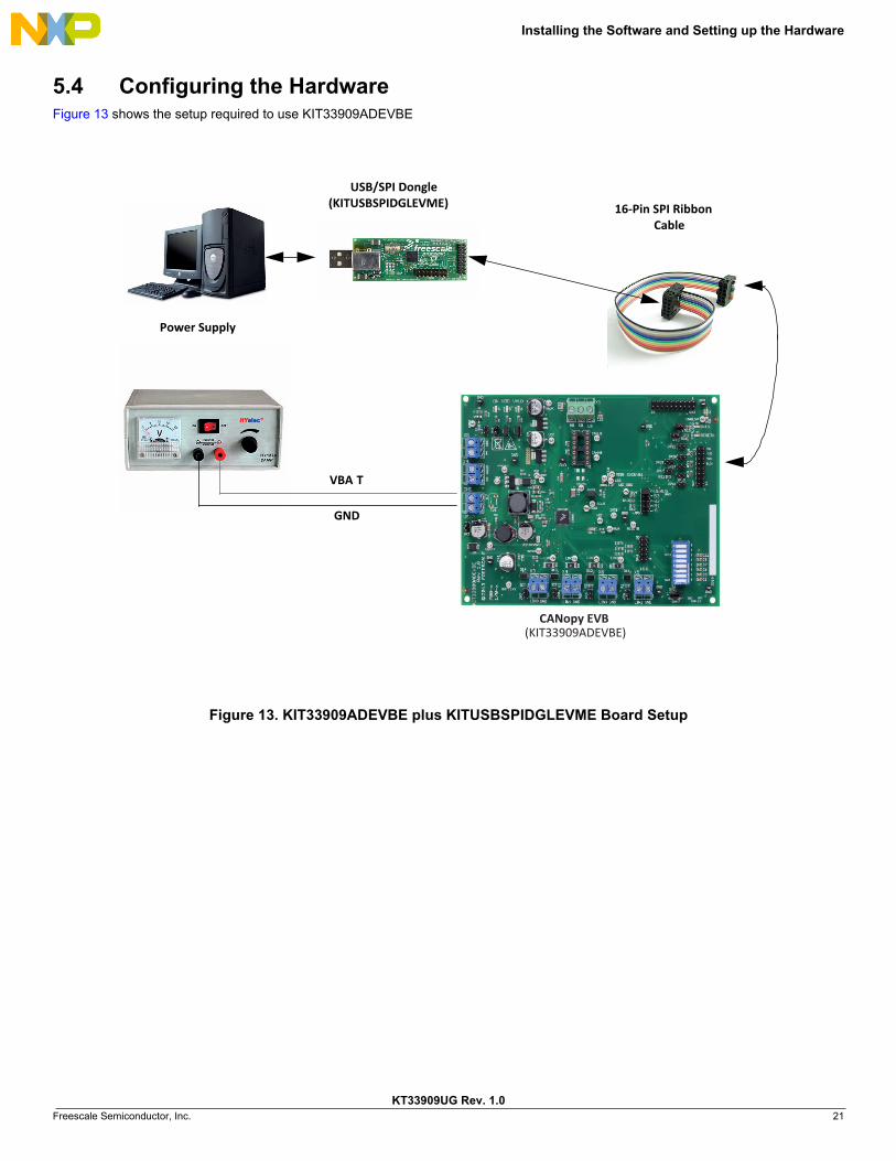
5.4 Configuring the HardwareFigure 13 shows the setup required to use KIT33909ADEVBE
Figure 13. KIT33909ADEVBE plus KITUSBSPIDGLEVME Board Setup
USB/SPI Dongle(KITUSBSPIDGLEVME) 16-Pin SPI Ribbon
Cable
Power Supply
GND
VBA T
CANopy EVB(KIT33909ADEVBE)

Installing the Software and Setting up the Hardware
KT33909UG Rev. 1.022 Freescale Semiconductor, Inc.
5.4.1 Step-by-step Instructions for Setting up the Hardware using SPIGenTo perform the demonstration examples, use following connections and setup procedure:
1. Ready the computer and install the SPIGen.
2. Connect a cable between the evaluation board connector SV1 and the SPI Dongle. Connect the USB cable from the SPI Dongle to the computer.
3. Set the EVB Jumpers and Switches as needed. (Refer to the jumper locations in Figure 6 and the jumper definitions in Table 10)
4. Attach the DC power supply (without turning on the power) to connector X7 for VSUP and GND.
5. Select the Safe Mode setting by using JP5. If the DEBUG mode (used to disable watchdog) is selected, an additional 12 V DC power supply must be connected to the WDI_DEBUG test point.
6. Attach loads to the board output connectors as desired.
7. Launch SPIGen and select the MC33909 Interface tab.
8. Turn on the DC power supply connected to the WDI_DEBUG test point.
9. Turn on the DC power supply connected to the X7 connector. At this point, the LED's for the "ON" and "VDD" voltage rails turn on and you can monitor the voltages. The WDI_DEBUG pin is at 12 V.
10. The IC will idle in the INIT state until a WD refresh word is sent. (There is no time limit in Watchdog inhibit mode.) While the IC is in the INIT state, enter the INIT word. (The INIT word can only be sent while the IC is in the INIT state.) All other words can also be sent while the IC is in INIT but some functions may not become active until Normal mode is entered.
11. Leave the INIT state by sending the WD refresh word (click in "Send Simple Refresh" under the WD Refresh tab) and operate the part as desired. May now turn on / off the various functions of the IC and test overall functionality.
Schematic
KT33909UG Rev. 1.0 Freescale Semiconductor, Inc. 23
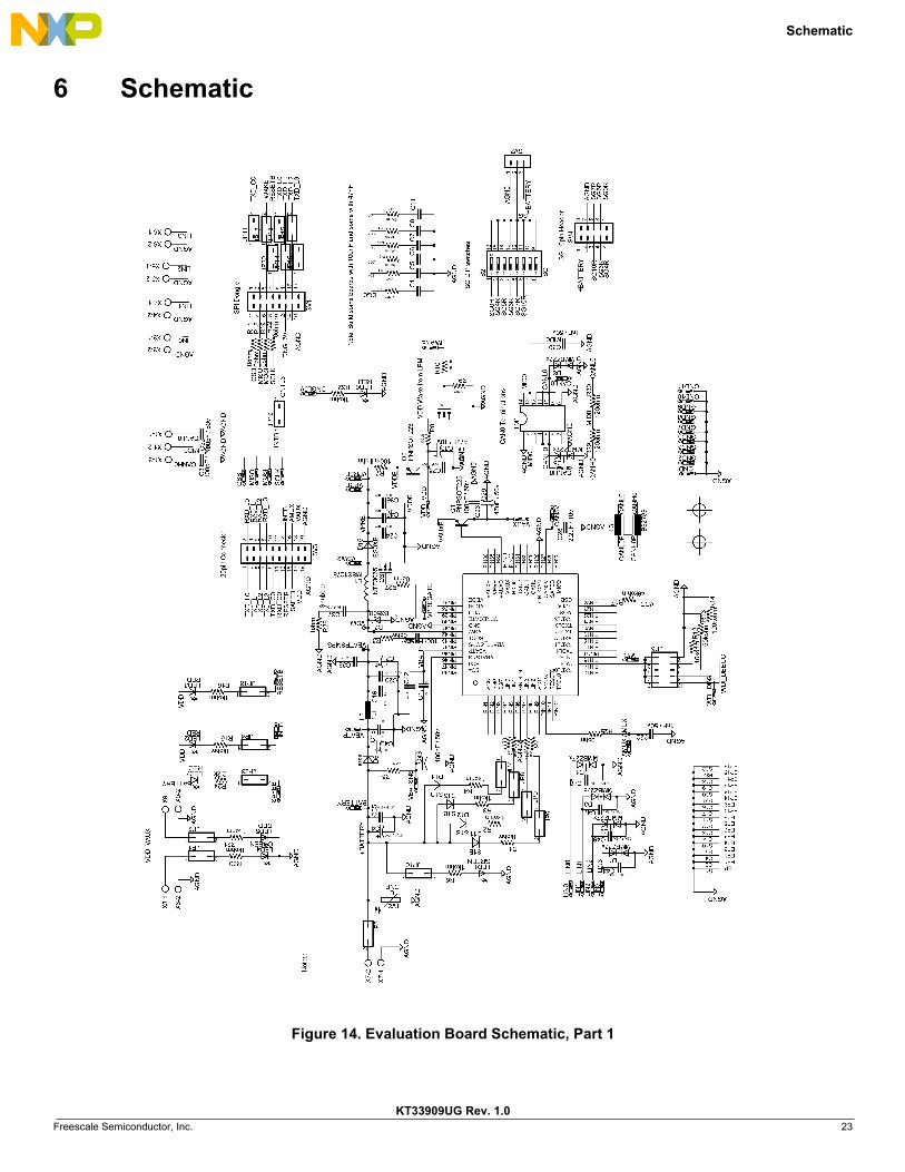
6 Schematic
Figure 14. Evaluation Board Schematic, Part 1
Board Layout
KT33909UG Rev. 1.024 Freescale Semiconductor, Inc.
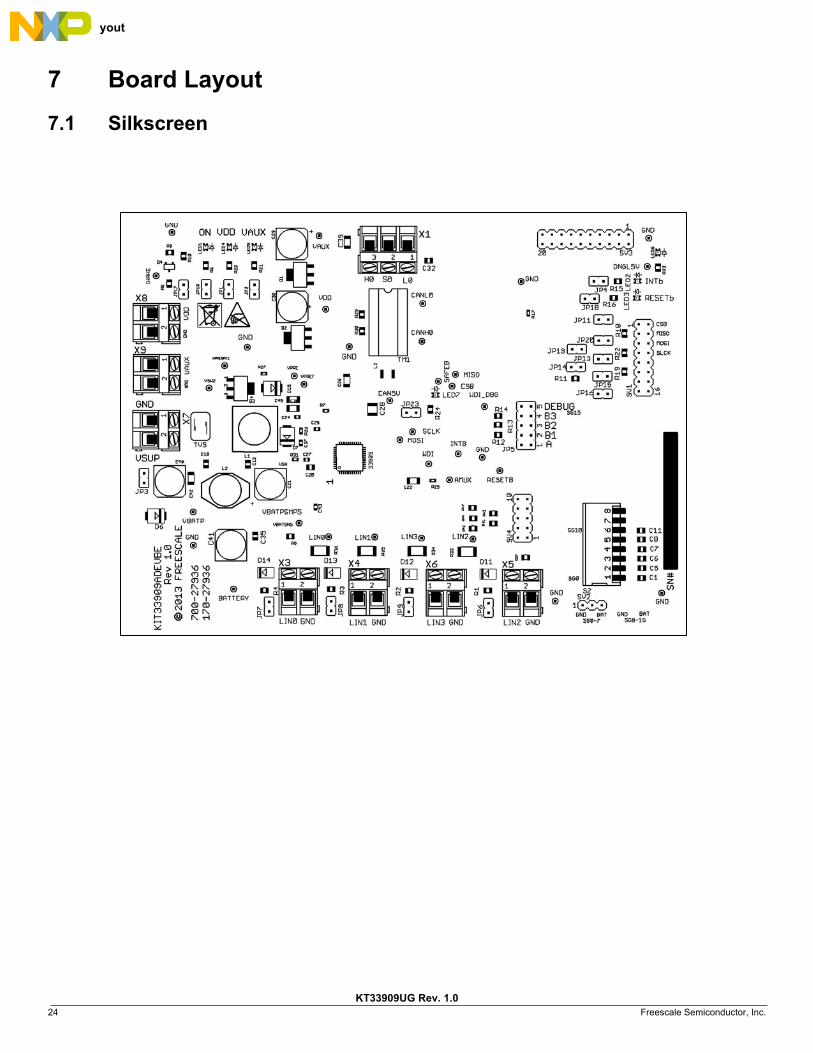
7 Board Layout
7.1 Silkscreen
Board Bill of Materials
KT33909UG Rev. 1.0 Freescale Semiconductor, Inc. 25
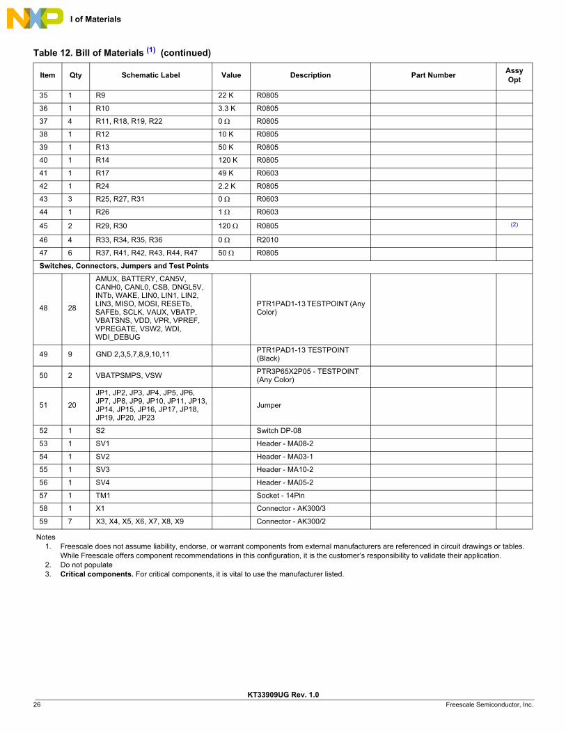
8 Board Bill of Materials
Table 12. Bill of Materials (1)
Item Qty Schematic Label Value Description Part NumberAssy Opt
Freescale Components
1 1 U1 CANopy MC33909Q5AD (3)
Inductors
2 1 L1 22 uH MSS1278 (Coilcraft) (3)
3 1 L2 3 uH DO3316P (3)
4 1 L3 B82789 SM-CAN-CHOKE
Transistors
5 2 Q1, Q2 PNPSOT223
6 1 Q3 NTF3055
7 1 Q4 MMBF0201NLT1G
Diodes
8 6 D1, D2, D3, D4, D5, D8 MMBZ27x
9 2 D6, D15 ES3XB (3 A)
10 1 D7 B350B (Vishay Schottky)
11 4 D11, D12, D13, D14 S1B (1 A)
12 2 LED1, LED4 CHIPLED - 0805 (Green)
13 5 LED2, LED3, LED5, LED6, LED7 CHIPLED - 0805 (Red)
Capacitors
14 8C1, C5, C6, C7, C8, C11, C18. C19
100 nF 50 V - C0805
15 1 C17 10 nF 50 V - C0603
16 1 C20 4.7 uF 50 V - C0805
17 2 C21, C40 22 uF 50 V - 153CLV-0807
18 2 C22, C39 1 nF 50 V - C1206
19 2 C24, C25 10 nF 10 V - C0603
20 1 C26 100 nF 50 V - C1206
21 2 C27, C43 100 nF 50 V - C0603
22 1 C28 2.2 uF 10 V - C1210
23 2 C29, C41 47 uF 50 V - 153CLV-0807
24 1 C30 47 uF 10 V - 153CLV-0807
25 2 C31, C32 100 pF 50 V - C0805
26 1 C35 100 nF 50 V - C0805
27 1 C36 10 uF 10 V - C1206
28 2 C37, C38 10 nF 50 V - C0603
29 1 C42 47 uF 50 V - C1206
30 4 C44, C46, C47, C48 220 pF 50 V - C0603
31 1 C45 47 uF 10 V - C1206
Resistors
32 11R1, R2, R3, R4, R5, R6, R15, R16, R20, R21, R32
1.0 K R0805
33 1 R7 100 m R0603
34 1 R8 300 R0805
Board Bill of Materials
KT33909UG Rev. 1.026 Freescale Semiconductor, Inc.
35 1 R9 22 K R0805
36 1 R10 3.3 K R0805
37 4 R11, R18, R19, R22 0 R0805
38 1 R12 10 K R0805
39 1 R13 50 K R0805
40 1 R14 120 K R0805
41 1 R17 49 K R0603
42 1 R24 2.2 K R0805
43 3 R25, R27, R31 0 R0603
44 1 R26 1 R0603
45 2 R29, R30 120 R0805 (2)
46 4 R33, R34, R35, R36 0 R2010
47 6 R37, R41, R42, R43, R44, R47 50 R0805
Switches, Connectors, Jumpers and Test Points
48 28
AMUX, BATTERY, CAN5V, CANH0, CANL0, CSB, DNGL5V, INTb, WAKE, LIN0, LIN1, LIN2, LIN3, MISO, MOSI, RESETb, SAFEb, SCLK, VAUX, VBATP, VBATSNS, VDD, VPR, VPREF, VPREGATE, VSW2, WDI, WDI_DEBUG
PTR1PAD1-13 TESTPOINT (Any Color)
49 9 GND 2,3,5,7,8,9,10,11PTR1PAD1-13 TESTPOINT (Black)
50 2 VBATPSMPS, VSWPTR3P65X2P05 - TESTPOINT (Any Color)
51 20
JP1, JP2, JP3, JP4, JP5, JP6, JP7, JP8, JP9, JP10, JP11, JP13, JP14, JP15, JP16, JP17, JP18, JP19, JP20, JP23
Jumper
52 1 S2 Switch DP-08
53 1 SV1 Header - MA08-2
54 1 SV2 Header - MA03-1
55 1 SV3 Header - MA10-2
56 1 SV4 Header - MA05-2
57 1 TM1 Socket - 14Pin
58 1 X1 Connector - AK300/3
59 7 X3, X4, X5, X6, X7, X8, X9 Connector - AK300/2
Notes 1. Freescale does not assume liability, endorse, or warrant components from external manufacturers are referenced in circuit drawings or tables.
While Freescale offers component recommendations in this configuration, it is the customer’s responsibility to validate their application.2. Do not populate3. Critical components. For critical components, it is vital to use the manufacturer listed.
Table 12. Bill of Materials (1) (continued)
Item Qty Schematic Label Value Description Part NumberAssy Opt

Accessory Item Bill of Materials
KT33909UG Rev. 1.0 Freescale Semiconductor, Inc. 27
9 Accessory Item Bill of Materials
Table 13. Bill of Materials (4)
Item Qty Part Number Description
1 1 KITUSBSPIDGLEVME SPIgen USB to EVB interface board
Notes 4. Freescale does not assume liability, endorse, or warrant components from external manufacturers are referenced in circuit drawings or tables.
While Freescale offers component recommendations in this configuration, it is the customer’s responsibility to validate their application.
References
KT33909UG Rev. 1.028 Freescale Semiconductor, Inc.
10 ReferencesFollowing are URLs where you can obtain information on related Freescale products and application solutions:
10.1 SupportVisit www.freescale.com/support for a list of phone numbers within your region.
10.2 WarrantyVisit www.freescale.com/warranty for a list of phone numbers within your region.
Freescale.com Support Pages
Description URL
KIT33909ADEVBE Tool Summary Page http://www.freescale.com/webapp/sps/site/prod_summary.jsp?code=KIT33909ADEVBE
MC33909 Product Summary Page http://www.freescale.com/webapp/sps/site/prod_summary.jsp?code=MC33909
MC33909 Datasheet http://www.freescale.com/files/analog/doc/data_sheet/MC33909.pdf
SPIGen Software http://www.freescale.com/files/soft_dev_tools/software/device_drivers/SPIGen.html
KITUSBSPIDGLEVME Tool Summary Page http://www.freescale.com/webapp/sps/site/prod_summary.jsp?code=KITUSBSPIDGLEVME
Analog Analog Home Page http://www.freescale.com/analog

Revision History
KT33909UG Rev. 1.0 Freescale Semiconductor, Inc. 29
11 Revision History
Revision Date Description of Changes
1.03/2015 Initial Release
4/2015 Corrected pin connections in Table 4
Document Number: KT33909UGRev. 1.0
4/2015
Information in this document is provided solely to enable system and software implementers to use Freescale products.
There are no express or implied copyright licenses granted hereunder to design or fabricate any integrated circuits based
on the information in this document.
Freescale reserves the right to make changes without further notice to any products herein. Freescale makes no
warranty, representation, or guarantee regarding the suitability of its products for any particular purpose, nor does
Freescale assume any liability arising out of the application or use of any product or circuit, and specifically disclaims any
and all liability, including without limitation consequential or incidental damages. “Typical” parameters that may be
provided in Freescale data sheets and/or specifications can and do vary in different applications, and actual performance
may vary over time. All operating parameters, including “typicals,” must be validated for each customer application by
customer’s technical experts. Freescale does not convey any license under its patent rights nor the rights of others.
Freescale sells products pursuant to standard terms and conditions of sale, which can be found at the following address:
freescale.com/SalesTermsandConditions.
Freescale and the Freescale logo are trademarks of Freescale Semiconductor, Inc., Reg. U.S. Pat. & Tm. Off.
SMARTMOS is a trademark of Freescale Semiconductor, Inc. All other product or service names are the property of their
respective owners.
© 2015 Freescale Semiconductor, Inc.
How to Reach Us:
Home Page: freescale.com
Web Support: freescale.com/support


![AN11913 BGU8019, GNSS, LNA, L2 - NXP Semiconductors · AN11915 BGU8309 [GPS1401M] tuned for GNSS L2-band evaluation board Rev. 1 — 17 July 2017 Application note Document information](https://img.pdfslide.us/doc/110x75/601d384fd93e38614c0119ac/an11913-bgu8019-gnss-lna-l2-nxp-semiconductors-an11915-bgu8309-gps1401m-tuned.jpg)