Embed Size (px)
Citation preview

AN11514 BGU8H1 LTE LNA evaluation board Rev. 3 — 22 January 2016 Application note
Document information Info Content Keywords BGU8H1, LTE, LNA
Abstract This document explains the BGU8H1 LTE LNA evaluation board
Ordering info Board-number: OM7886 12NC: 9340 686 51598
Contact information For more information, please visit: http://www.nxp.com

NXP Semiconductors AN11514 BGU8H1 LTE LNA EVB
AN11514 All information provided in this document is subject to legal disclaimers. © NXP B.V. 2016. All rights reserved.
Application note Rev. 3 — 22 January 2016 2 of 23
Contact information For more information, please visit: http://www.nxp.com For sales office addresses, please send an email to: [email protected]
Revision history Rev Date Description 3 2 1
20160122 20151120 20140423
Updated with extra application information Text paragraph 4.1 updated First publication

NXP Semiconductors AN11514 BGU8H1 LTE LNA EVB
AN11514 All information provided in this document is subject to legal disclaimers. © NXP B.V. 2016. All rights reserved.
Application note Rev. 3 — 22 January 2016 3 of 23
1. Introduction NXP Semiconductors’ BGU8H1 LTE LNA Evaluation Board is designed to evaluate the performance of the LTE LNA using:
NXP Semiconductors’ BGU8H1 LTE Low Noise Amplifier
A matching inductor
A decoupling capacitor
NXP Semiconductors’ BGU8H1 is a low-noise amplifier for LTE receiver applications in a plastic, leadless 6 pin, extremely thin small outline SOT1232 at 1.1 x 0.7 x 0.37mm, 0.4mm pitch. The BGU8H1 features gain of 13 dB and a noise figure of 0.9 dB at a current consumption of 5 mA. Its superior linearity performance removes interference and noise from co-habitation cellular transmitters, while retaining sensitivity. The LNA components occupy a total area of approximately 4 mm2.
In this document, the application diagram, board layout, bill of materials, and typical results are given, as well as some explanations on LTE related performance parameters like input third-order intercept point IIP3, gain compression and noise.
Fig 1. BGU8x1 LTE LNA evaluation board (used for BGU8L1, BGU8M1 and BGU8H1)

NXP Semiconductors AN11514 BGU8H1 LTE LNA EVB
AN11514 All information provided in this document is subject to legal disclaimers. © NXP B.V. 2016. All rights reserved.
Application note Rev. 3 — 22 January 2016 4 of 23
2. General description Modern cellular phones have multiple radio systems, so problems like co-habitation are quite common. Since the LTE diversity antenna needs to be placed far from the main antenna to ensure the efficiency of the channel, a low noise amplifier close to the antenna is used to compensate the track-losses (and SAW-filter losses when applicable) on the printed circuit board. A LTE receiver implemented in a mobile phone requires a low current consumption and low Noise Figure. All the different transmit signals that are active in smart phones and tablets can cause problems like inter-modulation and compression. Therefore also a high linearity is required.
3. BGU8H1 LTE LNA evaluation board The BGU8H1LNA evaluation board simplifies the RF evaluation of the BGU8H1 LTE LNA applied in a LTE front-end, often used in mobile cell phones. The evaluation board enables testing of the device RF performance and requires no additional support circuitry. The board is fully assembled with the BGU8H1 including the input series inductor and decoupling capacitor. The board is supplied with two SMA connectors for input and output connection to RF test equipment. The BGU8H1can operate from a 1.5 V to 3.1 V single supply and consumes typical 5 mA.
3.1 Application Circuit The circuit diagram of the evaluation board is shown in Fig 2. With jumper JU1 the enable input can be connected either to Vcc or GND.
Fig 2. Circuit diagram of the BGU8x1 LNA evaluation board (used for BGU8L1, BGU8M1 and BGU8H1)
4
1
BGU8x1
6
2
35
X3
GND Ven Vcc
X4
JU1
C1
L1
X1 X2
RF in RF out
BGU8x1LTE LNAEVB
C2

NXP Semiconductors AN11514 BGU8H1 LTE LNA EVB
AN11514 All information provided in this document is subject to legal disclaimers. © NXP B.V. 2016. All rights reserved.
Application note Rev. 3 — 22 January 2016 5 of 23
3.2 PCB Layout
Fig 3. Printed-Circuit Board layout of the BGU8x1LNA evaluation board (used for BGU8L1, BGU8M1 and BGU8H1)
A good PCB layout is an essential part of an RF circuit design. The LNA evaluation board of the BGU8H1 can serve as a guideline for laying out a board using the BGU8H1. Use controlled impedance lines for all high frequency inputs and outputs. Bypass Vcc with decoupling capacitors, preferably located as close as possible to the device. For long bias lines it may be necessary to add decoupling capacitors along the line further away from the device. Proper grounding of the GND pins is also essential for good RF performance. Either connect the GND pins directly to the ground plane or through vias, or do both, which is recommended. The material that has been used for the evaluation board is FR4 using the stack shown in Fig 4.
(1) Material supplier is ISOLA DURAVER; εr = 4.6-4.9: T
Fig 4. Stack of the PCB material
0.2mm FR4 critical
0.8mm FR4 only for mechanical rigidity of PCB
20um Cu
20um Cu
20um Cu

NXP Semiconductors AN11514 BGU8H1 LTE LNA EVB
AN11514 All information provided in this document is subject to legal disclaimers. © NXP B.V. 2016. All rights reserved.
Application note Rev. 3 — 22 January 2016 6 of 23
4. Bill of materials
Table 1. BOM of the BGU8H1 LTE LNA evaluation board Designator Description Footprint Value Supplier Name/type Comment F BGU8H1 1.1 x 0.7 x
0.37mm3, 0.4mm pitch
NXP SOT1232
PCB 20 x 35mm BGU8H1 LTE LNA EV Kit
C1 Capacitor 0402 1nF Murata GRM1555 Decoupling
C2 Capacitor 0402 1nF Murata GRM1555 Decoupling
L1 Inductor 0402 3.3nH Murata LQW15 Input matching
X1, X2 SMA RD connector
- - Johnson, End launch SMA 142-0701-841
RF input/ RF output
X3 DC header - - Molex, PCB header, Right Angle, 1 row, 3 way 90121-0763
Bias connector
X4 JUMPER Stage
- - Molex, PCB header, Vertical, 1 row, 3 way 90120-0763
Connect Ven to Vcc or separate Ven voltage
JU1 JUMPER
4.1 BGU8H1 NXP Semiconductors’ BGU8H1 LTE low noise amplifier is designed for the LTE frequency band. The integrated biasing circuit is temperature stabilized, which keeps the current constant over temperature. It also enables the superior linearity performance of the BGU8H1. The BGU8H1 is also equipped with an enable function that allows it to be controlled via a logic signal. In disabled mode it consumes less than1 μA.
The output of the BGU8H1 is internally matched between 2300 MHz and 2690 MHz whereas only one series inductor at the input is needed to achieve the best RF performance. The output is AC coupled via an integrated capacitor.
It requires only two external components to build a LTE LNA having the following advantages:
Low noise
System optimized gain
High linearity under jamming
1.1 x 0.7 x 0.37, 0.4mm pitch: SOT1232
Low current consumption
Short power settling time
4.2 Series inductor The evaluation board is supplied with Murata LQW15 series inductor of 3.3 nH. This is a wire wound type of inductor with high quality factor (Q) and low series resistance (Rs). This type of inductor is recommended in order to achieve the best noise performance. High Q inductors from other suppliers can be used. If it is decided to use other low cost inductors with lower Q and higher Rs the noise performance will degrade.

NXP Semiconductors AN11514 BGU8H1 LTE LNA EVB
AN11514 All information provided in this document is subject to legal disclaimers. © NXP B.V. 2016. All rights reserved.
Application note Rev. 3 — 22 January 2016 7 of 23
5. Required Equipment In order to measure the evaluation board the following is necessary:
DC Power Supply op to 30 mA at 1.5 V to 3.1 V
Two RF signal generators capable of generating RF signals at the LTE operating frequency between 2300 MHz and 2690 MHz.
An RF spectrum analyzer that covers at least the operating frequency between 2300 MHz and 2690 MHz as well as a few of the harmonics. Up to 6 GHz should be sufficient. “Optional” a version with the capability of measuring noise figure is convenient
Amp meter to measure the supply current (optional)
A network analyzer for measuring gain, return loss and reverse isolation
Noise figure analyzer and noise source
Directional coupler
Proper RF cables
6. Connections and setup The BGU8H1 LTE LNA evaluation board is fully assembled and tested (see Fig 5). Please follow the steps below for a step-by-step guide to operate the LNA evaluation board and testing the device functions. 1. Connect the DC power supply to the Vcc and GND terminals. Set the power supply to
the desired supply voltage, between 1.5 V and 3.1 V, but never exceed 3.1 V as it might damage the BGU8H1.
2. Jumper JU1 is connected between the Vcc terminal of the evaluation board and the Ven pin of the BGU8H1.
3. Connect the RF signal generator and the spectrum analyzer to the RF input and the RF output of the evaluation board, respectively. Do not turn on the RF output of the signal generator yet, set it to approximately -40 dBm output power at center frequency of the wanted LTE-ban and\ set the spectrum analyzer at the same center frequency and a reference level of 0 dBm.
4. Turn on the DC power supply and it should read approximately 4..5 mA. 5. Enable the RF output of the generator: The spectrum analyzer displays a tone
around –27 dBm. 6. Instead of using a signal generator and spectrum analyzer one can also use a
network analyzer in order to measure gain as well as in- and output return loss, P1dB and IP3 (see Fig 6).
7. For noise figure evaluation, either a noise figure analyzer or a spectrum analyzer with noise option can be used. The use of a 5 dB noise source, like the Agilent 364B is recommended. When measuring the noise figure of the evaluation board, any kind of adaptors, cables etc between the noise source and the evaluation board should be minimized, since this affects the noise figure (see Fig 7).

NXP Semiconductors AN11514 BGU8H1 LTE LNA EVB
AN11514 All information provided in this document is subject to legal disclaimers. © NXP B.V. 2016. All rights reserved.
Application note Rev. 3 — 22 January 2016 8 of 23
Fig 5. Evaluation board including its connections
Fig 6. 2-Tone Setup for 50Ω LNA board tests (S-Parameters, P1dB and 2-Tone-tests)

NXP Semiconductors AN11514 BGU8H1 LTE LNA EVB
AN11514 All information provided in this document is subject to legal disclaimers. © NXP B.V. 2016. All rights reserved.
Application note Rev. 3 — 22 January 2016 9 of 23
Fig 7. Setup diagram for 50Ω LNA-board NF-Measurements.

NXP Semiconductors AN11514 BGU8H1 LTE LNA EVB
AN11514 All information provided in this document is subject to legal disclaimers. © NXP B.V. 2016. All rights reserved.
Application note Rev. 3 — 22 January 2016 10 of 23
7. Evaluation Board Tests
7.1 S-Parameters
The measured S-Parameters and stability factor K are given in the figures below. For the measurements, a BGU8H1-LNA EVB is used ((see Fig 5). Measurements have been carried out using the setup shown in Fig 6.
Fig 8. BGU8H1 S-Parameters (typical values). Vcc=2.8V, Pin=-45dBm.
-30
-25
-20
-15
-10
-5
0
5
10
15
20
0.0E+00 2.0E+09 4.0E+09 6.0E+09 8.0E+09 1.0E+10
S21
[dB
]
Freq [Hz]
S21 (dB)
-80
-70
-60
-50
-40
-30
-20
-10
0
0.0E+00 2.0E+09 4.0E+09 6.0E+09 8.0E+09 1.0E+10
S12
[dB
]
Freq [Hz]
S12(dB)
-30
-25
-20
-15
-10
-5
0
0.0E+00 2.0E+09 4.0E+09 6.0E+09 8.0E+09 1.0E+10
Spar
[dB
]
Freq [Hz]
S11 & S22
S11
S22
0.01
0.1
1
10
100
1000
0.0E+00 2.0E+09 4.0E+09 6.0E+09 8.0E+09 1.0E+10
K-fa
ctor
Freq [Hz]
K-factor

NXP Semiconductors AN11514 BGU8H1 LTE LNA EVB
AN11514 All information provided in this document is subject to legal disclaimers. © NXP B.V. 2016. All rights reserved.
Application note Rev. 3 — 22 January 2016 11 of 23
Fig 9. BGU8H1 S-Parameters (typical values). Vcc=2.8V, Pin=-45dBm (freq. range zoomed in).
10
11
12
13
14
15
16
2.2E+09 2.4E+09 2.6E+09 2.8E+09
S21
[dB
]
Freq [Hz]
S21 (dB)
-40
-35
-30
-25
-20
-15
-10
2.2E+09 2.4E+09 2.6E+09 2.8E+09
S12
[dB
]
Freq [Hz]
S12(dB)
-30
-25
-20
-15
-10
-5
0
2.2E+09 2.4E+09 2.6E+09 2.8E+09
Spar
[dB
]
Freq [Hz]
S11 & S22
1
1.1
1.2
1.3
1.4
1.5
1.6
1.7
1.8
1.9
2
2.2E+09 2.4E+09 2.6E+09 2.8E+09
K-fa
ctor
Freq [Hz]
K-factor
NXP Semiconductors AN11514 BGU8H1 LTE LNA EVB
AN11514 All information provided in this document is subject to legal disclaimers. © NXP B.V. 2016. All rights reserved.
Application note Rev. 3 — 22 January 2016 12 of 23
7.2 1dB gain compression Strong in-band cell phone TX jammers can cause linearity problems and result in third-order intermodulation products in the LTE frequency band. In this chapter the effects of these strong signals is shown. For the measurements, a BGU8H1-LNA EVB is used ((see Fig 5). Measurements have been carried out using the setup shown in Fig 6 The gain as function of input power of the DUT was measured between port RFin and RFout of the EVB at the LTE center frequencies. The figures below show the gain compression curves at LNA-board.
Fig 10. Gain versus inp. power , f=2350MHz (band 40) Fig 11. Gain versus input power , f=2655MHz (band 7)
0
2
4
6
8
10
12
14
16
-30 -25 -20 -15 -10 -5 0
Gai
n [
dB
]
Pin [dBm]
BGU8H1, 50745#1P1dB, f=2350MHz
Vcc=1.8V
Vcc=2.8V
Vcc=3.1V
Vcc=1.5V
0
2
4
6
8
10
12
14
16
-30 -25 -20 -15 -10 -5 0
Gai
n [
dB
]
Pin [dBm]
BGU8H1, 50745#1P1dB, f=2655MHz
Vcc=1.8V
Vcc=2.8V
Vcc=3.1V
Vcc=1.5V

NXP Semiconductors AN11514 BGU8H1 LTE LNA EVB
AN11514 All information provided in this document is subject to legal disclaimers. © NXP B.V. 2016. All rights reserved.
Application note Rev. 3 — 22 January 2016 13 of 23
7.3 2-Tone Test
The figures below show the spectra of the DUT caused by a 2-Tone input signal around the centre of the LTE-bands. For the measurements, a BGU8H1-LNA EVB is used ((see Fig 5). Measurements have been carried out using the setup shown in Fig 6.
Fig 12. Gain versus input power, band 40 Fig 13. Gain versus input power, band 7
-100
-90
-80
-70
-60
-50
-40
-30
-20
-10
0
2.34E+09 2.35E+09 2.36E+09 2.37E+09 2.38E+09
Po
ut
[dB
m]
Freq [Hz]
BGU8H1_50745#12-Tone Test, band 40
Vcc=1.8V
Vcc=2.8V
Vcc=3.1V
Vcc=1.5V
-100
-90
-80
-70
-60
-50
-40
-30
-20
-10
0
2.64E+09 2.65E+09 2.66E+09 2.67E+09 2.68E+09
Po
ut
[dB
m]
Freq [Hz]
BGU8M1_50744#12-Tone Test, band 7
Vcc=1.8V
Vcc=2.8V
Vcc=3.1V
Vcc=1.5V

NXP Semiconductors AN11514 BGU8H1 LTE LNA EVB
AN11514 All information provided in this document is subject to legal disclaimers. © NXP B.V. 2016. All rights reserved.
Application note Rev. 3 — 22 January 2016 14 of 23
7.4 Enable Timing Test The following diagram shows the setup to test LNA Turn ON and Turn OFF time. Set the waveform generator to square mode and the output amplitude at 3Vrms with high output impedance. The waveform generator has adequate output current to drive the LNA therefore no extra DC power supply is required which simplifies the test setup. Set the RF signal generator output level to -20dBm between 2300 MHz and 2690 MHz and increase its level until the output DC on the oscilloscope is at 5mV on 1mV/division, the signal generator RF output level is approximately -3dBm. It is very important to keep the cables as short as possible at input and output of the LNA so the propagation delay difference on cables between the two channels is minimized. It is also critical to set the oscilloscope input impedance to 50ohm on channel 2 so the diode detector can discharge quickly to avoid a false result on the Turn OFF time testing.
Fig 14. Setup Enable Timing Test The series capacitor will influence the Ton/Toff switching time. When the default value C2=1nF is used, Ton will approximately be 9us. By reducing C2 to 100pF, Ton is reduced to approximately 4µs (see Fig 15 and Fig 16).

NXP Semiconductors AN11514 BGU8H1 LTE LNA EVB
AN11514 All information provided in this document is subject to legal disclaimers. © NXP B.V. 2016. All rights reserved.
Application note Rev. 3 — 22 January 2016 15 of 23
Fig 15. Results Enable Timing Test. Series capacitor C2=1nF. Ton~9µs (left) and Toff~200ns (right).
Fig 16. Results Enable Timing Test. Series capacitor C2=100pF. Ton~4µs (left).

NXP Semiconductors AN11514 BGU8H1 LTE LNA EVB
AN11514 All information provided in this document is subject to legal disclaimers. © NXP B.V. 2016. All rights reserved.
Application note Rev. 3 — 22 January 2016 16 of 23
8. Typical LNA evaluation board results
Table 2. Typical results measured on the evaluation Board.
Typical LNA evaluation board resultsTemp = 25 °C
Parameter Symbol Unit NoteFreq. [MHz]
Supply Voltage Vcc 1.5 1.8 2.8 3.1 VSupply Current Icc 4.3 4.8 5.0 5.0 mA
Noise Figure 2350 NF 1.0 1.0 1.0 1.0 dB2655 1.2 1.2 1.1 1.1 [1]
Power Gain 2350 Gp 12.7 13.0 13.0 13.3 dB2655 11.7 12.0 12.5 12.3
Input Return Loss 2350 RLin 7 8 9 8 dB2655 8 8 9 9
Output Return Loss 2350 RLout 22 20 20 23 dB2655 27 20 20 26
Reverse Isolation 2350 ISOrev 22 20 22 22 dB2655 22 20 22 22
Input 1dB Gain Compression 2350 Pi1dB -11.7 -8.0 -3.0 -0.5 dBm2655 -10.2 -7.0 -1.0 0.6
Output 1dB Gain Compression 2350 Po1dB 0.0 4.0 9.0 11.8 dBm2655 0.5 4.0 10.5 11.9
Input third order intercept point 2350 IIP3 -2.7 2.0 6.0 5.4 dBm [2]2655 -0.8 5.0 8.0 8.6
Output third order intercept point 2350 OIP3 10.0 15.0 19.0 18.7 dBm [2]2655 10.9 17.0 20.5 20.9
Power settling time Ton 4 4 4 4 µsToff 1 1 1 1 µs
[1] Including PCB losses[2] f = f_center_band; Delta_f=10MHz
Pin_f1 = Pin_f2 = -15 dBm

NXP Semiconductors AN11514 BGU8H1 LTE LNA EVB
AN11514 All information provided in this document is subject to legal disclaimers. © NXP B.V. 2016. All rights reserved.
Application note Rev. 3 — 22 January 2016 17 of 23
9. Improved in band blocking performance modification In some cases a strong in-band jamming signal is present, reducing the sensitivity. This in band blocking test case in illustrated below in Fig 17. A jamming signal causes an increase of the noise-floor closely around the jamming frequency, which reduces the sensitivity for a wanted signal overlapping with the noise band.
Fig 17. Example in band blocking test case A solution is to make a low impedance path for low frequencies at the input of the LNA. This can be done by an additional shunt inductor L2 with a high value, as shown in the circuit of Fig 18 and board detail in Fig 19 (L1 and C2 have been swapped compared with Fig 2 to avoid a DC-path between RFin and GND). For L2 a Murata LQW15 wire wound inductor with a value of 82nH is used.
Fig 18. Circuit diagram of modified BGU8x1 LTE LNA evaluation board (L2=82nH)
4
1
BGU8x1
6
2
35
X3
GND Ven Vcc
X4
JU1
C1
L1
X1 X2
RF in RF out
BGU8x1LTE LNAEVB
C2
L2

NXP Semiconductors AN11514 BGU8H1 LTE LNA EVB
AN11514 All information provided in this document is subject to legal disclaimers. © NXP B.V. 2016. All rights reserved.
Application note Rev. 3 — 22 January 2016 18 of 23
Fig 19. Detail of modified BGU8x1 LTE LNA evaluation board The measured performance is given in Fig 20 and Table 3. The Gain and the NF are almost equal for both versions.
Fig 20. Measured performance modified BGU8x1 LTE LNA evaluation board
NXP Semiconductors AN11514 BGU8H1 LTE LNA EVB
AN11514 All information provided in this document is subject to legal disclaimers. © NXP B.V. 2016. All rights reserved.
Application note Rev. 3 — 22 January 2016 19 of 23
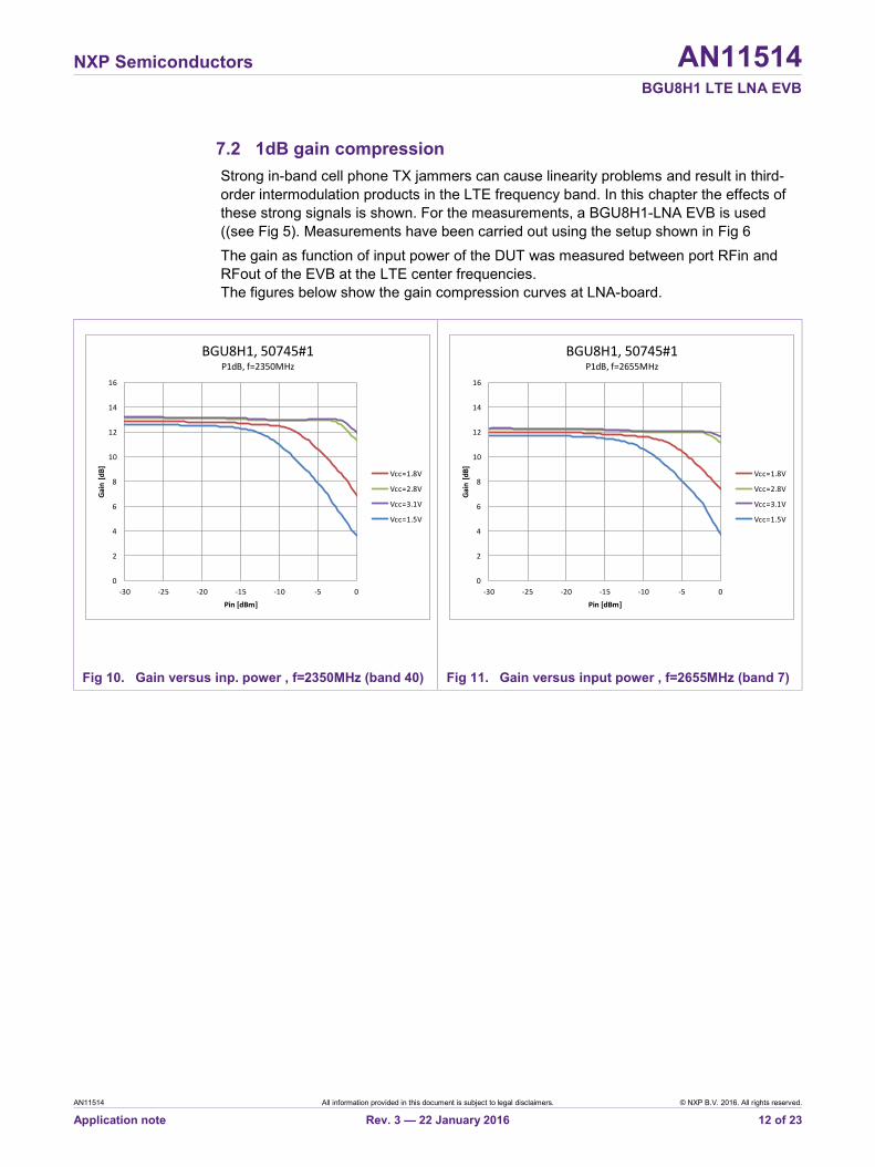
Table 3. Typical results measured on the modified evaluation Board.
Note: Noise Figure is including PCB losses.
Typical LNA evaluation board resultsTemp [°C] 25 BU8H1_157716P_Spar [dBm] -45 3 EVB's
Default L2=82nH DeltaParameter Symbol typ typ typ Unit Notes
Freq. [MHz]Supply Voltage Vcc 2.80V 2.80V 2.80V V
Noise Figure 2350 NF dB2500 1.05 1.04 -0.012655
Power Gain 2350 Gp 13.0 12.8 -0.1 dB2500 12.5 12.3 -0.22655 12.0 11.7 -0.2
Input Return Loss 2350 RLin 8.7 6.2 -2.5 dB2500 8.3 6.0 -2.32655 8.5 5.9 -2.6
Output Return Loss 2350 RLout 20.6 17.9 -2.7 dB2500 22.7 20.4 -2.22655 23.5 23.6 0.1
Reverse Isolation 2350 ISOrev 22.7 22.9 0.2 dB2500 22.5 22.7 0.22655 22.4 22.6 0.2
Input 1dB Gain Compression 2350 Pi1dB -0.8 -0.3 0.5 dBm2500 -0.3 0.5 0.82655 0.4 1.0 0.6
Output 1dB Gain Compression 2350 Po1dB 11.1 11.5 0.4 dBm2500 11.2 11.8 0.72655 11.3 11.7 0.4
Input third order intercept point 2350 IIP3 4.2 4.3 0.1 dBm(average lsb&usb) 2500 5.7 6.3 0.6
2655 5.7 6.2 0.5Output third order intercept point2350 OIP3 17.4 17.6 0.2 dBm(average lsb&usb) 2500 18.1 18.8 0.7
2655 17.4 18.1 0.7

Error!
Unknow
n docume
nt property nam
e.
Error! Unknow
n document property nam
e. E
rror! Unknow
n document property
name.
NXP Semiconductors AN11514 BGU8H1 LTE LNA EVB
AN11514 All information provided in this document is subject to legal disclaimers. © NXP B.V. 2016. All rights reserved.
Application note Rev. 3 — 22 January 2016 20 of 23
10. Legal information
10.1 Definitions Draft — The document is a draft version only. The content is still under internal review and subject to formal approval, which may result in modifications or additions. NXP Semiconductors does not give any representations or warranties as to the accuracy or completeness of information included herein and shall have no liability for the consequences of use of such information.
10.2 Disclaimers Limited warranty and liability — Information in this document is believed to be accurate and reliable. However, NXP Semiconductors does not give any representations or warranties, expressed or implied, as to the accuracy or completeness of such information and shall have no liability for the consequences of use of such information. NXP Semiconductors takes no responsibility for the content in this document if provided by an information source outside of NXP Semiconductors.
In no event shall NXP Semiconductors be liable for any indirect, incidental, punitive, special or consequential damages (including - without limitation - lost profits, lost savings, business interruption, costs related to the removal or replacement of any products or rework charges) whether or not such damages are based on tort (including negligence), warranty, breach of contract or any other legal theory.
Notwithstanding any damages that customer might incur for any reason whatsoever, NXP Semiconductors’ aggregate and cumulative liability towards customer for the products described herein shall be limited in accordance with the Terms and conditions of commercial sale of NXP Semiconductors.
Right to make changes — NXP Semiconductors reserves the right to make changes to information published in this document, including without limitation specifications and product descriptions, at any time and without notice. This document supersedes and replaces all information supplied prior to the publication hereof.
Suitability for use — NXP Semiconductors products are not designed, authorized or warranted to be suitable for use in life support, life-critical or safety-critical systems or equipment, nor in applications where failure or malfunction of an NXP Semiconductors product can reasonably be expected to result in personal injury, death or severe property or environmental damage. NXP Semiconductors and its suppliers accept no liability for inclusion and/or use of NXP Semiconductors products in such equipment or applications and therefore such inclusion and/or use is at the customer’s own risk.
Applications — Applications that are described herein for any of these products are for illustrative purposes only. NXP Semiconductors makes no representation or warranty that such applications will be suitable for the specified use without further testing or modification.
Customers are responsible for the design and operation of their applications and products using NXP Semiconductors products, and NXP Semiconductors accepts no liability for any assistance with applications or customer product design. It is customer’s sole responsibility to determine whether the NXP Semiconductors product is suitable and fit for the customer’s applications and products planned, as well as for the planned application and use of customer’s third party customer(s). Customers should provide appropriate design and operating safeguards to minimize the risks associated with their applications and products.
NXP Semiconductors does not accept any liability related to any default, damage, costs or problem which is based on any weakness or default in the customer’s applications or products, or the application or use by customer’s third party customer(s). Customer is responsible for doing all necessary testing for the customer’s applications and products using NXP Semiconductors products in order to avoid a default of the applications and the products or of the application or use by customer’s third party customer(s). NXP does not accept any liability in this respect.
Export control — This document as well as the item(s) described herein may be subject to export control regulations. Export might require a prior authorization from national authorities.
Evaluation products — This product is provided on an “as is” and “with all faults” basis for evaluation purposes only. NXP Semiconductors, its affiliates and their suppliers expressly disclaim all warranties, whether express, implied or statutory, including but not limited to the implied warranties of non-infringement, merchantability and fitness for a particular purpose. The entire risk as to the quality, or arising out of the use or performance, of this product remains with customer.
In no event shall NXP Semiconductors, its affiliates or their suppliers be liable to customer for any special, indirect, consequential, punitive or incidental damages (including without limitation damages for loss of business, business interruption, loss of use, loss of data or information, and the like) arising out the use of or inability to use the product, whether or not based on tort (including negligence), strict liability, breach of contract, breach of warranty or any other theory, even if advised of the possibility of such damages.
Notwithstanding any damages that customer might incur for any reason whatsoever (including without limitation, all damages referenced above and all direct or general damages), the entire liability of NXP Semiconductors, its affiliates and their suppliers and customer’s exclusive remedy for all of the foregoing shall be limited to actual damages incurred by customer based on reasonable reliance up to the greater of the amount actually paid by customer for the product or five dollars (US$5.00). The foregoing limitations, exclusions and disclaimers shall apply to the maximum extent permitted by applicable law, even if any remedy fails of its essential purpose.
10.3 Trademarks Notice: All referenced brands, product names, service names and trademarks are property of their respective owners.

NXP Semiconductors AN11514 BGU8H1 LTE LNA EVB
AN11514 All information provided in this document is subject to legal disclaimers. © NXP B.V. 2016. All rights reserved.
Application note Rev. 3 — 22 January 2016 21 of 23
11. List of figures
Fig 1. BGU8x1 LTE LNA evaluation board (used for BGU8L1, BGU8M1 and BGU8H1) .................... 3
Fig 2. Circuit diagram of the BGU8x1 LNA evaluation board (used for BGU8L1, BGU8M1 and BGU8H1) .......................................................... 4
Fig 3. Printed-Circuit Board layout of the BGU8x1LNA evaluation board (used for BGU8L1, BGU8M1 and BGU8H1) ................................................... 5
Fig 4. Stack of the PCB material ................................. 5 Fig 5. Evaluation board including its connections ....... 8 Fig 6. 2-Tone Setup for 50Ω LNA board tests (S-
Parameters, P1dB and 2-Tone-tests) ............... 8 Fig 7. Setup diagram for 50Ω LNA-board NF-
Measurements. ................................................. 9 Fig 8. BGU8H1 S-Parameters (typical values).
Vcc=2.8V, Pin=-45dBm. .................................. 10 Fig 9. BGU8H1 S-Parameters (typical values).
Vcc=2.8V, Pin=-45dBm (freq. range zoomed in). ........................................................................ 11
Fig 10. Gain versus inp. power , f=2350MHz (band 40) ........................................................................ 12
Fig 11. Gain versus input power , f=2655MHz (band 7) ........................................................................ 12
Fig 12. Gain versus input power, band 40 .................. 13 Fig 13. Gain versus input power, band 7 .................... 13 Fig 14. Setup Enable Timing Test ............................... 14 Fig 15. Results Enable Timing Test. Series capacitor
C2=1nF. Ton~9µs (left) and Toff~200ns (right). ........................................................................ 15
Fig 16. Results Enable Timing Test. Series capacitor C2=100pF. Ton~4µs (left). .............................. 15
Fig 17. Example in band blocking test case ................ 17 Fig 18. Circuit diagram of modified BGU8x1 LTE LNA
evaluation board (L2=82nH) ........................... 17 Fig 19. Detail of modified BGU8x1 LTE LNA evaluation
board ............................................................... 18 Fig 20. Measured performance modified BGU8x1 LTE
LNA evaluation board ..................................... 18

NXP Semiconductors AN11514 BGU8H1 LTE LNA EVB
AN11514 All information provided in this document is subject to legal disclaimers. © NXP B.V. 2016. All rights reserved.
Application note Rev. 3 — 22 January 2016 22 of 23
12. List of tables
Table 1. BOM of the BGU8H1 LTE LNA evaluation board .......................................................................... 6
Table 2. Typical results measured on the evaluation Board. ............................................................. 16
Table 3. Typical results measured on the modified evaluation Board. ............................................ 19

NXP Semiconductors AN11514 BGU8H1 LTE LNA EVB
Please be aware that important notices concerning this document and the product(s) described herein, have been included in the section 'Legal information'.
© NXP B.V. 2016. All rights reserved.
For more information, visit: http://www.nxp.com For sales office addresses, please send an email to: [email protected]
Date of release: 22 January 2016 Document identifier: AN11514
13. Contents
1. Introduction ......................................................... 3 2. General description ............................................. 4 3. BGU8H1 LTE LNA evaluation board .................. 4 3.1 Application Circuit .............................................. 4 3.2 PCB Layout ........................................................ 5 4. Bill of materials .................................................... 6 4.1 BGU8H1 ............................................................. 6 4.2 Series inductor ................................................... 6 5. Required Equipment ........................................... 7 6. Connections and setup ....................................... 7 7. Evaluation Board Tests .................................... 10 7.1 S-Parameters ................................................... 10 7.2 1dB gain compression ...................................... 12 7.3 2-Tone Test ...................................................... 13 7.4 Enable Timing Test .......................................... 14 8. Typical LNA evaluation board results ............. 16 9. Improved in band blocking performance
modification ....................................................... 17 10. Legal information .............................................. 20 10.1 Definitions ........................................................ 20 10.2 Disclaimers....................................................... 20 10.3 Trademarks ...................................................... 20 11. List of figures ..................................................... 21 12. List of tables ...................................................... 22 13. Contents ............................................................. 23