Embed Size (px)
Citation preview
Semiconductor Physics of Lasing and Exciton Condensation etc.
Kanika Bansal, Arthur Varghese, Padmashri Patil
Amit Bhunia, Saurav Kumar, Mayur Shinde, Mohit Singh
Shouvik Datta, Dept. of Physics, IISER-Pune
Anton Ego: “Yes, I think I do. After reading a lot of overheated puffery about your new cook, you know what I'm craving? A little perspective.
That's it. I'd like some fresh, clear, well seasoned perspective.Can you suggest a good wine to go with that? ”
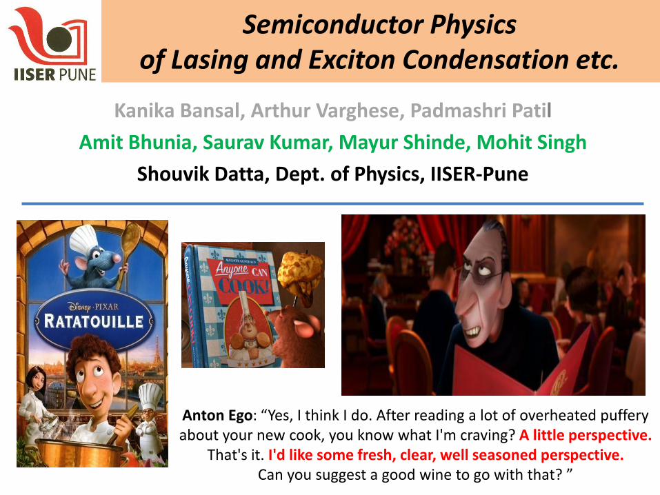
Past & Current Research Things We have been Asking…
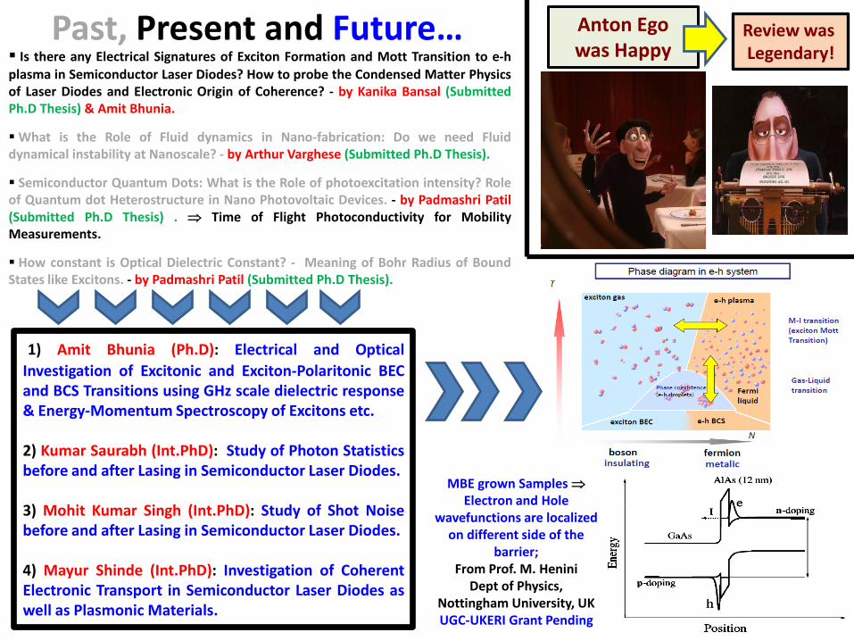
Are there any Electrical Signatures of Exciton Formation and MottTransition to e-h plasma in Semiconductor Laser Diodes? How to probethe Condensed Matter Physics of Laser Diodes and Electronic Origin ofCoherence? - by Kanika Bansal (Submitted Ph.D Thesis) & Amit Bhunia.
What is the Role of Fluid dynamics in Nano-fabrication: Do we needFluid dynamical instability at Nanoscale? - by Arthur Varghese(Submitted Ph.D Thesis).
Semiconductor Quantum Dots: What is the - Role of photoexcitationintensity Fluorescence Blinking? Role of Quantum dot Heterostructure inNano Photovoltaic Devices? - by Padmashri Patil (Submitted PhD Thesis).
How constant is Optical Dielectric Constant? - Meaning of Bohr Radiusof Bound States like Excitons. - by Padmashri Patil (Submitted Ph.DThesis).
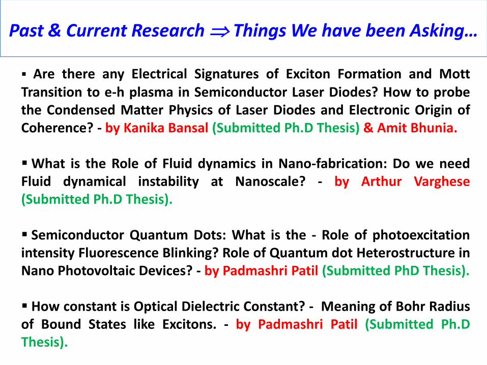
Ongoing & Future Research Things We Will be Asking…
1) Amit Bhunia (Ph.D): Electrical and Optical Investigation of Excitonic andExciton-Polaritonic BEC and BCS Transitions. Energy-Momentum Spectroscopy ofExcitons etc.
2) Kumar Saurabh (Int.PhD): Study of Photon Statistics before and after Lasing inSemiconductor Laser Diodes.
3) Mohit Kumar Singh (Int.PhD): Study of Shot Noise before and after Lasing inSemiconductor Laser Diodes.
4) Mayur Shinde (Int.PhD): Investigation of Coherent Electronic Transport inSemiconductor Laser Diodes as well as Plasmonic Materials.
How to connect all these following issues to probe the Electronic Origin of Coherence in Lasing and Excitonic BEC etc ?
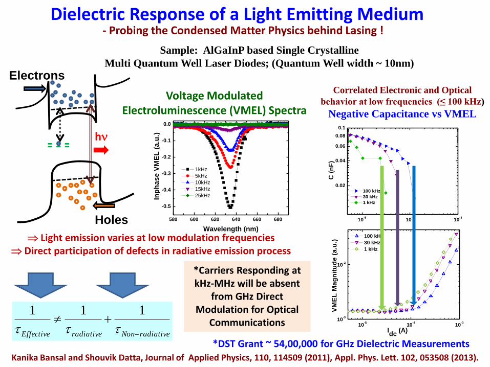
Dielectric Response of a Light Emitting Medium
radiativeNonradiativeEffective
111
Correlated Electronic and Optical
behavior at low frequencies (≤ 100 kHz)
Negative Capacitance vs VMEL
Light emission varies at low modulation frequencies Direct participation of defects in radiative emission process
Kanika Bansal and Shouvik Datta, Journal of Applied Physics, 110, 114509 (2011), Appl. Phys. Lett. 102, 053508 (2013)..
Sample: AlGaInP based Single Crystalline
Multi Quantum Well Laser Diodes; (Quantum Well width ~ 10nm)
Electrons
Holes 580 600 620 640 660 680
-0.5
-0.4
-0.3
-0.2
-0.1
0.0
1kHz
5kHz
10kHz
15kHz
25kHz
Inp
ha
se
VM
EL
(a
.u.)
Wavelength (nm)
Voltage Modulated Electroluminescence (VMEL) Spectra
- Probing the Condensed Matter Physics behind Lasing !
h
*DST Grant ~ 54,00,000 for GHz Dielectric Measurements
10-5
10-4
10-3
10-3
10-2
100 kHz
30 kHz
1 kHz
VM
EL
Ma
gn
itu
de
(a
.u.)
Idc
(A)
10-5
10-4
10-3
0.02
0.04
0.06
0.08
0.1
100 kHz
30 kHz
1 kHz
C (
nF
)
*Carriers Responding at kHz-MHz will be absent
from GHz Direct Modulation for Optical
Communications
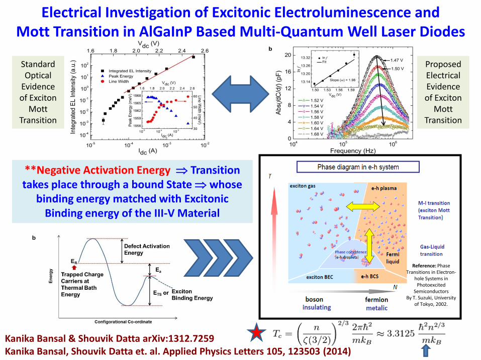
Electrical Investigation of Excitonic Electroluminescence and Mott Transition in AlGaInP Based Multi-Quantum Well Laser Diodes
Kanika Bansal & Shouvik Datta arXiv:1312.7259Kanika Bansal, Shouvik Datta et. al. Applied Physics Letters 105, 123503 (2014)
**Negative Activation Energy Transition takes place through a bound State whose
binding energy matched with Excitonic Binding energy of the III-V Material
Reference: Phase Transitions in Electron-
hole Systems in Photoexcited
SemiconductorsBy T. Suzuki, University
of Tokyo, 2002.
Standard Optical
Evidence of Exciton
Mott Transition
ProposedElectricalEvidence of Exciton
Mott Transition
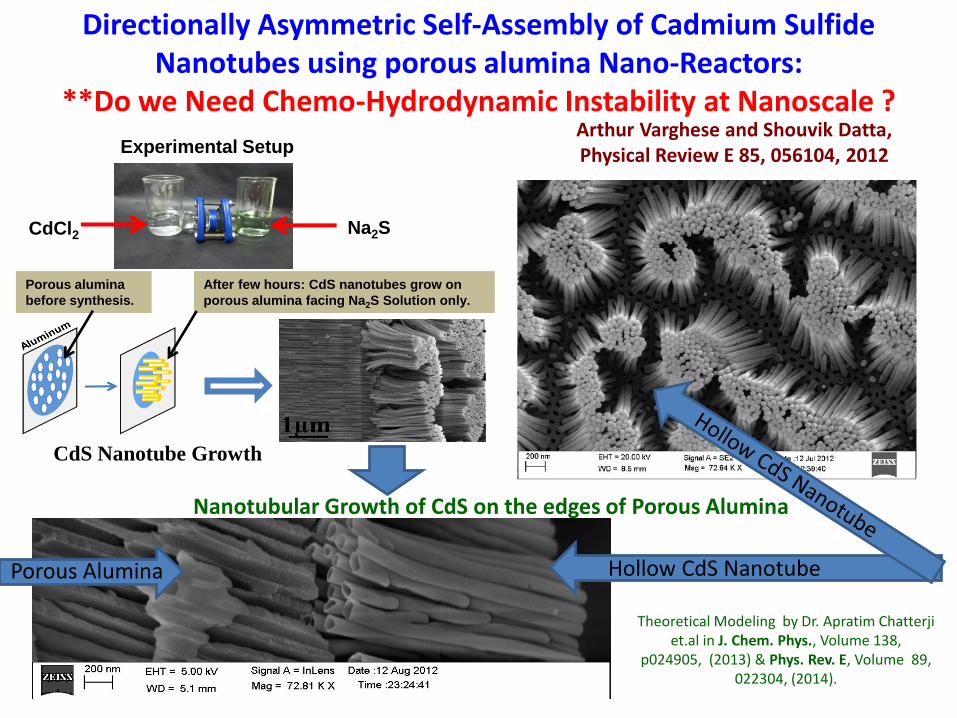
Directionally Asymmetric Self-Assembly of Cadmium Sulfide Nanotubes using porous alumina Nano-Reactors:
**Do we Need Chemo-Hydrodynamic Instability at Nanoscale ?
Nanotubular Growth of CdS on the edges of Porous Alumina
Porous Alumina Hollow CdS Nanotube
Experimental Setup
Na2SCdCl2
CdS Nanotube Growth
Porous alumina
before synthesis.
After few hours: CdS nanotubes grow on
porous alumina facing Na2S Solution only.
Arthur Varghese and Shouvik Datta, Physical Review E 85, 056104, 2012
Theoretical Modeling by Dr. Apratim Chatterjiet.al in J. Chem. Phys., Volume 138,
p024905, (2013) & Phys. Rev. E, Volume 89, 022304, (2014).
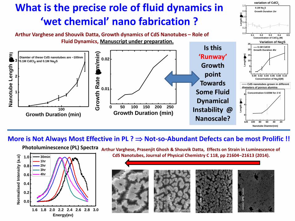
What is the precise role of fluid dynamics in ‘wet chemical’ nano fabrication ?
1.6 1.8 2.0 2.2 2.4 2.6 2.8 3.0
0.0
0.2
0.4
0.6
0.8
1.0
No
rma
lis
ed
In
ten
sit
y (
a.u
)
Energy(ev)
30min
1hr
2hr
3hr
4hr
More is Not Always Most Effective in PL ? Not-so-Abundant Defects can be most Prolific !!
0.00 0.02 0.04 0.06 0.08 0.10
0
5
10
15
20
25
Le
ng
th(
m)
Concertration of Na2S(M)
0.1M CdCl2
Growth Duration 4hr
Variation of Na2S
0.1 0.2 0.3 0.4 0.50.0
0.2
0.4
0.6
0.8
1.0variation of CdCl
2
Le
ng
th (m
)
Concentration of CdCl2 (M)
0.1M Na2S
Growth Duration 1hr
120 100 80 60 40 20
0
4
8Concentration 0.025M for 2 hr
Le
ng
th (m
)
Nanotube Diamter(nm)
CdS nanotubes grown in different
diameters of porous alumina
Arthur Varghese and Shouvik Datta, Growth dynamics of CdS Nanotubes – Role of Fluid Dynamics, Manuscript under preparation.
Arthur Varghese, Prasenjit Ghosh & Shouvik Datta, Effects on Strain in Luminescence of CdS Nanotubes, Journal of Physical Chemistry C 118, pp 21604–21613 (2014).
100
1
2
3
Na
no
tub
e L
en
gth
(m
)
Growth Duration (min)
Diamter of these CdS nanotubes are ~100nm
0.1M CdCl2 and 0.1M Na2S
0 50 100 150 200 250
0.01
0.02
Gro
wth
Ra
te (m
/min
)
Growth Duration (min)
Is this ‘Runway’Growth
point Towards
Some Fluid Dynamical
Instability @ Nanoscale?
Photoluminescence (PL) Spectra
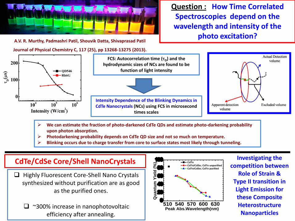
CdTe/CdSe Core/Shell NanoCrystals
We can estimate the fraction of photo-darkened CdTe QDs and estimate photo-darkening probability upon photon absorption.
Photodarkening probability depends on CdTe QD size and not so much on temperature. Blinking occurs due to charge transfer from core to surface states most likely through tunneling.
Highly Fluorescent Core-Shell Nano Crystals synthesized without purification are as good
as the purified ones.
~300% increase in nanophotovoltaicefficiency after annealing.
510 540 570 600 6300
20
40
60
80
100Q
ua
ntu
m Y
ield
(%
)
Peak Abs.Wavelength(nm)
CdTe
CdTe/CdSe; CdTe unpurified
CdTe/CdSe; CdTe purified
Investigating the competition between
Role of Strain &Type II transition in Light Emission for these Composite Heterostructure Nanoparticles
Question : How Time Correlated Spectroscopies depend on the wavelength and intensity of the
photo excitation?
FCS: Autocorrelation time (D) and the hydrodynamic sizes of NCs are found to be
function of light intensity
Intensity Dependence of the Blinking Dynamics in CdTe Nanocrystals (NCs) using FCS in microsecond
times scales
A.V. R. Murthy, Padmashri Patil, Shouvik Datta, Shivaprasad Patil
Journal of Physical Chemistry C, 117 (25), pp 13268-13275 (2013).
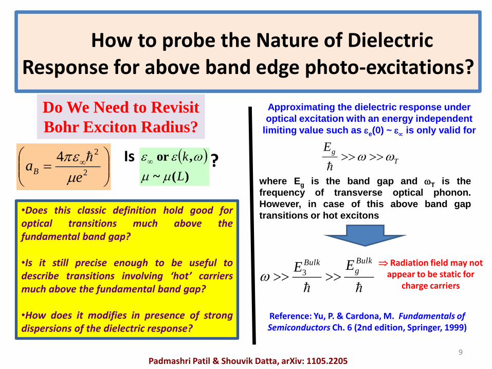
How to probe the Nature of Dielectric Response for above band edge photo-excitations?
9
•Does this classic definition hold good foroptical transitions much above thefundamental band gap?
•Is it still precise enough to be useful todescribe transitions involving ‘hot’ carriersmuch above the fundamental band gap?
•How does it modifies in presence of strongdispersions of the dielectric response?
2
24
eaB
Do We Need to Revisit
Bohr Exciton Radius?
)(~
,or
L
k
?Is
Padmashri Patil & Shouvik Datta, arXiv: 1105.2205
Approximating the dielectric response under
optical excitation with an energy independent
limiting value such as e(0) ~ is only valid for
T
gE
where Eg is the band gap and T is the
frequency of transverse optical phonon.
However, in case of this above band gap
transitions or hot excitons
Bulk
gBulk EE
3 Radiation field may not
appear to be static for charge carriers
Reference: Yu, P. & Cardona, M. Fundamentals of Semiconductors Ch. 6 (2nd edition, Springer, 1999)
1) Amit Bhunia (Ph.D): Electrical and Optical
Investigation of Excitonic and Exciton-Polaritonic BECand BCS Transitions using GHz scale dielectric response& Energy-Momentum Spectroscopy of Excitons etc.
2) Kumar Saurabh (Int.PhD): Study of Photon Statisticsbefore and after Lasing in Semiconductor Laser Diodes.
3) Mohit Kumar Singh (Int.PhD): Study of Shot Noisebefore and after Lasing in Semiconductor Laser Diodes.
4) Mayur Shinde (Int.PhD): Investigation of CoherentElectronic Transport in Semiconductor Laser Diodes aswell as Plasmonic Materials.
Past, Present and Future…
MBE grown Samples Electron and Hole
wavefunctions are localized on different side of the
barrier; From Prof. M. Henini
Dept of Physics, Nottingham University, UKUGC-UKERI Grant Pending
Is there any Electrical Signatures of Exciton Formation and Mott Transition to e-hplasma in Semiconductor Laser Diodes? How to probe the Condensed Matter Physicsof Laser Diodes and Electronic Origin of Coherence? - by Kanika Bansal (SubmittedPh.D Thesis) & Amit Bhunia.
What is the Role of Fluid dynamics in Nano-fabrication: Do we need Fluiddynamical instability at Nanoscale? - by Arthur Varghese (Submitted Ph.D Thesis).
Semiconductor Quantum Dots: What is the Role of photoexcitation intensity? Roleof Quantum dot Heterostructure in Nano Photovoltaic Devices. - by Padmashri Patil(Submitted Ph.D Thesis) . Time of Flight Photoconductivity for MobilityMeasurements.
How constant is Optical Dielectric Constant? - Meaning of Bohr Radius of BoundStates like Excitons. - by Padmashri Patil (Submitted Ph.D Thesis).
Review was Legendary!
Anton Ego was Happy