Embed Size (px)
Citation preview

June 12 to 15, 2011San Diego, CA
Multi‐tip Probe (MtP) Contacts forMulti tip Probe (MtP) Contacts for Flip Chip Wafer Level Probing
Norman Armendariz, Ph.D.@ [email protected]
James [email protected]
TEST TECHNOLOGY CENTER INFRASTRUCTURE

Overview• Introduction• Approach• Qualification Test FlowsQ
– Technology Qualification– Production Qualification
• Effect of OT on CRes• Effect of OT on CRes• Effect of Cleaning Frequency• Actual Over Travel• Comparative Analyses
– Electrical– Mechanical
• Summary of Multi‐tip Probe (MtP) Attributes• Conclusion• Acknowledgements
June 12 to 15, 2011 IEEE SW Test Workshop 2
• Acknowledgements

Introduction• Multi site probing of Flip Chip devices with pin counts• Multi-site probing of Flip Chip devices with pin-counts
approaching 12000 pins will physically strain the current mechanical test cell infrastructure capability and with increased electrical performance also requiredincreased electrical performance also required.
• Currently, CVPC- conventional vertical probe cards are used to probe Flip-Chip devices (~170um pitch 100um diaused to probe Flip-Chip devices ( 170um pitch, 100um dia. solder bumps) w/~7000 pins.
• The cost of probe cards are also expected to increase• The cost of probe cards are also expected to increase, primarily due to the need for custom interconnections. Typically, MLC-multi-layered substrates, are used to interconnect to the PCB.interconnect to the PCB.
• Moreover, if these tips can leverage a similar MLC inherent to current FFI-Formfactor probe card construction then ato current FFI-Formfactor probe card construction, then a cost effective approach would also be facilitated.

Approach• A TI / FFI strategic probe development effort was initiated
to MEMs fabricate probe tips on existing FFI MicroSpring® technology to validate the multi‐tip “probe physics” on solder bumped featuressolder bumped features.
• A comparative analysis was then performed to determine if b tt b l ti i t f l t i l dif a better probe solution, in terms of electrical and physical performance would result vs. current C‐VPC technology based on a test vehicle with ~4,000 spherical solder bumps at ~170um pitchsolder bumps at 170um pitch.
• Probe qualification and integration based on a 2‐step process;process; – 1‐Technology Qualification: to validate technology– 2‐Production Qualification: to determine production worthiness.

MtP / FFI-Micro-spring Probe Card TechnologyMicro Springs w/ MEMS used to form “Crown” tips, similar to WSP pogo-pin crown-tips, may offer a better COO when scaling from x1 to x4 multi-site applications, since the MLC-multi-layered ceramic is inherent in both.
Various crown tips or features can be custom fabricated on theVarious crown tips or features can be custom fabricated on the micro-spring to optimize probing with the micro-springs fabricated on an MLC for multi-site.

QUALIFICATION TEST FLOW: MtP vs. C-VPC
MtPMtP
Dallas Test Floor Production Test Floor
TEST FLOORS
MtP/FFIMtP
PROD QUAL
MtP TECH QUAL
MtP RTP
IN PROCESS
PASS
NO NOSTEP 1 STEP 2
C-VPC WST SET-UP
C-VPC RTP
C-VPC WST TI-BASELINE
Comparative probe card analysis performed in parallel to CVPC to minimize risk to production delivery, if MtP did not work.

1‐Technology Qualification Test FlowObjective: Define a stable probe / cleaning process and HW set-up before volume production qualification phase.
M P
MtP Probe Cards Re-Probed #2 8 Wafers
MtP CARD 2Wafer
1TestCell
# 1Wafer
2Wafer
2Wafer
3Wafer
4Stop for Tech Qual Review
MtP CARD 1
I V i bl
TestCell# 2
CVPC CARD
1
Wafer2
Wafer3 Control Reference
Output Variables:Input Variables:• Probe Card to Probe Card• Wafer to Wafer (Re‐probe)
Output Variables:• CRes• Yield• Re‐Probe Rate
• Throughput• Bump Scrub Damage• Planarity/AlignmentRe Probe Rate Planarity/Alignment

TQ: Effect of Over‐travel on CRes
Better contact performance (low CRes) is observed as OT‐over‐travel increases, but minimum of 60um is needed to achieve a good stable contact.
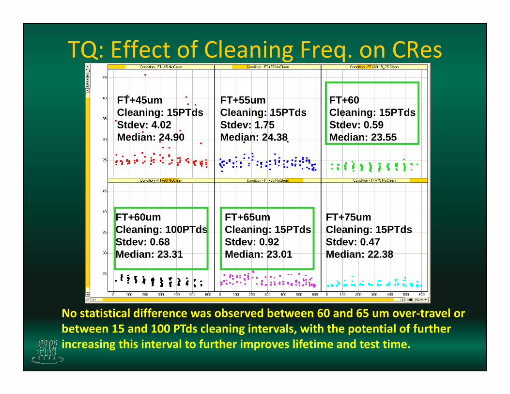
TQ: Effect of Cleaning Freq. on CRes
FT+45umCleaning: 15PTdsStd 4 02
FT+55umCleaning: 15PTdsStd 1 75
FT+60Cleaning: 15PTdsStd 0 59Stdev: 4.02
Median: 24.90Stdev: 1.75Median: 24.38
Stdev: 0.59Median: 23.55
FT+75umFT+65umFT+60umCleaning: 15PTdsStdev: 0.47Median: 22.38
Cleaning: 15PTdsStdev: 0.92Median: 23.01
Cleaning: 100PTdsStdev: 0.68Median: 23.31
No statistical difference was observed between 60 and 65 um over‐travel or between 15 and 100 PTds cleaning intervals, with the potential of further increasing this interval to further improves lifetime and test time.

TQ: Actual MtP Deflection in Test Cell
– Programmed Over‐Travel (POT) Th Z t
Program Over-travel um (POT)
(POT): The Z‐movement of the prober chuck in the z‐axis in the test cell.
AOTum
– Actual Over‐travel (AOT): Th t l Z t /The actual Z‐movement / compression of the Multi Point Tip’s micro‐spring
Dummy Wafer in the test cell.
Prober Chuck

Actual MtP Deflection in Test Cell• Based on the in‐situ “Clay Puck” tests, the actual over‐
travel (AOT) in the test cell was measured to be 40um ( )with a POT of FT+100um.
• In other words a programmed over travel (POT) set at• In other words, a programmed over‐travel (POT) set at FT+100um is equivalent to 40um of actual over‐travel (AOT).
• As a result, the current and stable programmed over‐travel (POT) recipe was defined based on this characterization to within the capabilities of the MtP micro‐spring deflection range and with an effective lower force required than if 100um was the AOT.q

TQ: MtP vs. CVPC Electrical Correlation
C-VPC MtP #1
MtP#2Wafer#1
Wafer#1
MtP#2
WaferWafer#1
Same wafer was probed with C‐VPC and both HD2’s cardsMtP‐1 600/603 (99.5%) Bin to Bin correlation to C‐VPCMtP‐2 597/603 (99 2%) Bin to Bin correlation to C‐VPCMtP‐2 597/603 (99.2%) Bin to Bin correlation to C‐VPC
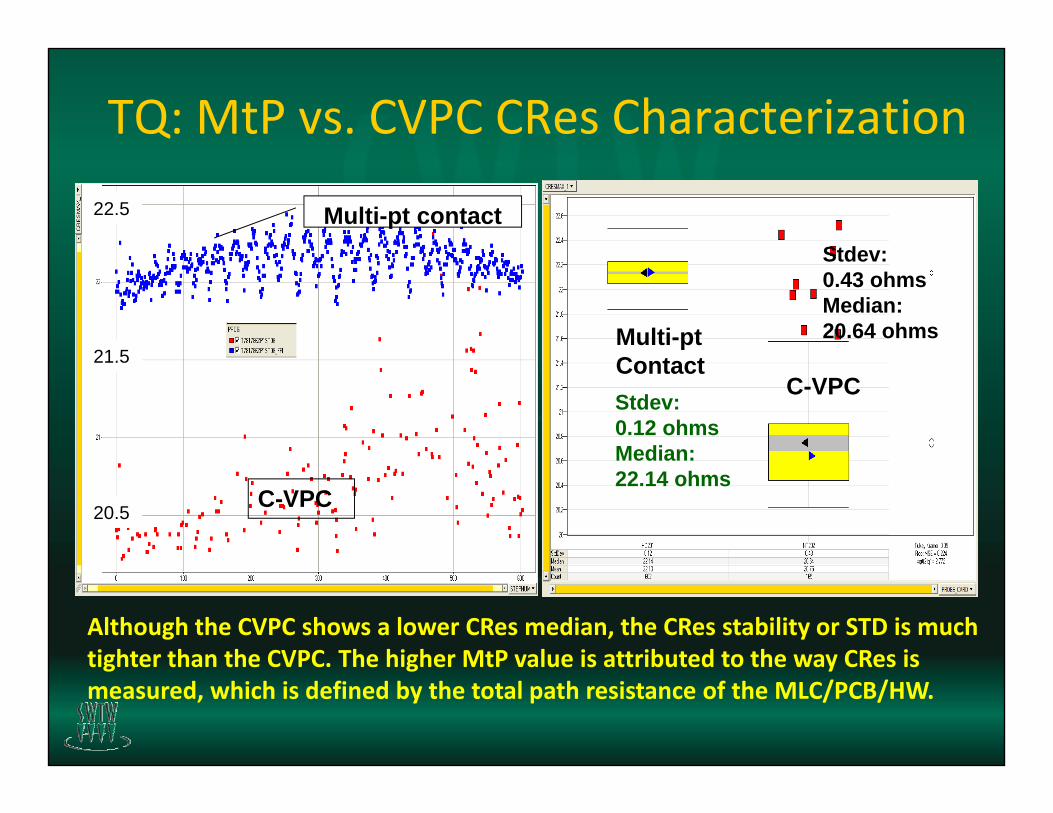
TQ: MtP vs. CVPC CRes Characterization
Multi-pt contactStdev:
22.5
Multi-pt
Stdev: 0.43 ohmsMedian: 20.64 ohms
21 5 ContactC-VPC
Stdev: 0.12 ohmsMedian:
21.5
C-VPC
Median: 22.14 ohms
20.5
Although the CVPC shows a lower CRes median, the CRes stability or STD is much tighter than the CVPC. The higher MtP value is attributed to the way CRes istighter than the CVPC. The higher MtP value is attributed to the way CRes is measured, which is defined by the total path resistance of the MLC/PCB/HW.

2‐Production Qualification Test FlowObjective: To validate long term stability of probe card / set-up and probe process reliability (Production Worthiness)
MtP LOTSTestCell LOTS
100 WafersSplit 4 Lots
MtP Probe Cards
CARD1
1A,2ATestCell
# 1
Parallel Test Flow (Multi-Test Cell
3A,4A
LOTsTestCell LOTsMtP
RTP
(Multi Test Cell setups)
LOTs1B,2B
TestCell# 2
LOTs3B,4BCARD
2
I V i bl Output Variables:Input Variables:• Probe Card to Probe Card• Wafer to Wafer (Re‐probe)
Output Variables:• CRes• Yield• Re‐Probe Rate
• TPT• Bump Scrub Damage• Planarity/Alignment
• Lot to LotRe Probe Rate Planarity/Alignment
• Lifetime/Reliability

PQ: MtP Production CRes Stability
Test Cell A Test Cell CTest Cell BTest Cell A
Lot#4
Test Cell CTest Cell B
Lot#1 Lot#2 Lot#3
Continuous production lots ran during production qualification checkout demonstrated contact stability over many consecutive wafers probed. This y y pvalidated the process recipe stability and margin for production fan out.

PQ: MtP Electrical Test Reliability
‐Re‐probe rate is very low w/ an average of 0.12% out of 40K die probed.‐Yield recovery from re‐probe related to contact was extremely low.‐Implies: mis‐contact is negligible and 1st Pass Yield is maximized‐Implies: mis‐contact is negligible and 1st Pass Yield is maximized

C‐VPC vs. MtP: Effect on Bump
MtPC-VPC Flat probes
MtP
CVPC Flat probes compress or impact the apex of the bump
Multi‐tip contacts create small dimple marks away from the apex
MtP
impact the apex of the bump. Bump height damage > 1/3 of the bump is not desirable. Also,
dimple marks away from the apex of bump; not affecting bump height. The pointed tips better
h b ’ d lCRes not as stable thus, more frequent cleaning to remove compacted debris is required.
penetrate the bump’s oxide layer, resulting in stable CRes using much lower probe force.p q p

Key Learning: “Probe Physics”• The pressure between any two (2) surfaces in
contact with each other is a function of force and contact area.
Force = Pressure x Contact Area
• Multi Point tip enables a lower force perArea 1
• Multi‐Point tip enables a lower force per probe creating adequate pressure to break into the surface of the bump to make a reliable electrical contact.
Flat Tip C-VPC
• To achieve the same effect, the corresponding flat tip of a C‐VPC approach would requires a larger force to collapse the surface oxide of the bump apex
Area 2surface oxide of the bump apex
• The electrical contact surface area; however is comparable where the sides of the pyramid provide sufficient surface area for
Multi-Point Contact
py a d p o de su c e t su ace a ea oelectrical conduction.

Summary of MTP Attributes
• Self alignment of tips to bump. Well centered
• No reflow of bump after probe is required
• CRes < C‐VPC
• Force/Pin < C‐VPC
• Cleaning < C‐VPC
• Planarization not required
• Cost Of Ownership < C‐VPC (Multi‐Site)
Conclusion• Multi-tip Probe contacts with the “piercing” action,
demonstrated a stable and production worthy contact mechanism for Flip Chip bump probing using a lowermechanism for Flip Chip bump probing using a lower force solution than the C-VPC
• The lower force exhibited by the MtP probe enables a path for a viable high pin-count / multi-site configurations probe solution with a lower Cost Of Ownership (COO)( )
• When this technology successfully completes the Production Qualification phase and if meets TI COOProduction Qualification phase and if meets TI COO targets, then it will be deployed to test floors as production volumes warrant.

Acknowledgements
• Carey Farley• Dien Ho
• Frank Meza• Tim Lillie
• Stan Ferrell• Dan Stillman
b
• Doug Shuey• Barry Naseck
• Jim Oborny