Embed Size (px)
Citation preview
JOURNAL OF DISPLAY TECHNOLOGY, VOL. 5, NO. 12, DECEMBER 2009 541
Dual-Plate OLED Display (DOD) Embedded WithWhite OLED
Chang-Wook Han, Hwa Kyung Kim, Hee Suk Pang, Sung-Hoon Pieh, Chang Je Sung, Hong Seok Choi,Woo-Chan Kim, Myung-Seop Kim, and Yoon-Heung Tak
Abstract—White organic light-emitting diode (WOLED) withcolor filter adopting dual-plate OLED display (DOD) structureis proposed. In order to prevent outgassing from color filter andovercoat, the SiN passivation film was deposited on the overcoatfilm. This structure does not show any defects after it has beenkept over 500 hours of storage tests at 90 C. By fabricating 1stacked WOLED consisting of fluorescent blue layer/ phospho-rescent red:green layer, luminance efficiency of 20 cd/A withCIEx � � ��, CIEy � � �� was achieved.
Index Terms—Barrier layer, color filter, dual-plate organic light-emitting diode (OLED) display (DOD), white OLED (WOLED) .
I. INTRODUCTION
I T IS WELL KNOWN that fine-metal mask (FMM) methodis not suitable for full color active-matrix organic light-
emitting diode (AMOLED) display prepared on a large-sizedsubstrate, due to its rather inaccurate precision in alignment ofthe mask with the substrate. Also, dark spots, which are causedas the glass substrate is in contact with FMM, are consideredas serious problem. Considering these problems, white organiclight-emitting diode (WOLED) is expected to become a strongcandidate for AMOLED display adopting larger than 5th Gen-eration substrate, owing to their advantages of high resolution,low cost and FMM-less method [1]–[4].
In general, when WOLED and color filter (CF) are em-bedded into AMOLED panel, two types of panel structure,such as, bottom and top emitting structure may be considered,depending on emitting direction. In the bottom emitting struc-ture, WOLED, CF and thin-film transistor (TFT) are fabricatedon the same substrate. This structure has some drawbacks inrespect to fabrication process, aperture ratio and CF-outgassing.On the other hand, top emitting structure has a serious problemin electrical resistance of semitransparent cathode to get uni-form brightness. Moreover, due to the unwanted microcavityeffect between a reflective lower electrode and a semi-reflectiveupper electrode, there is limitation to emitting the visible lightin the wide wavelength range [5], [6].
Manuscript received February 16, 2009; revised May 05, 2009. Current ver-sion published November 18, 2009.
The authors are with the OLED Technology Development Division, LGDisplay Company, Ltd., Paju-si Gyeonggi-do, 413-811, Korea (e-mail:[email protected]; [email protected]; [email protected]; [email protected]; [email protected]; [email protected];[email protected]; [email protected]; [email protected]).
Color versions of one or more of the figures in this paper are available onlineat http://ieeexplore.ieee.org.
Digital Object Identifier 10.1109/JDT.2009.2024009
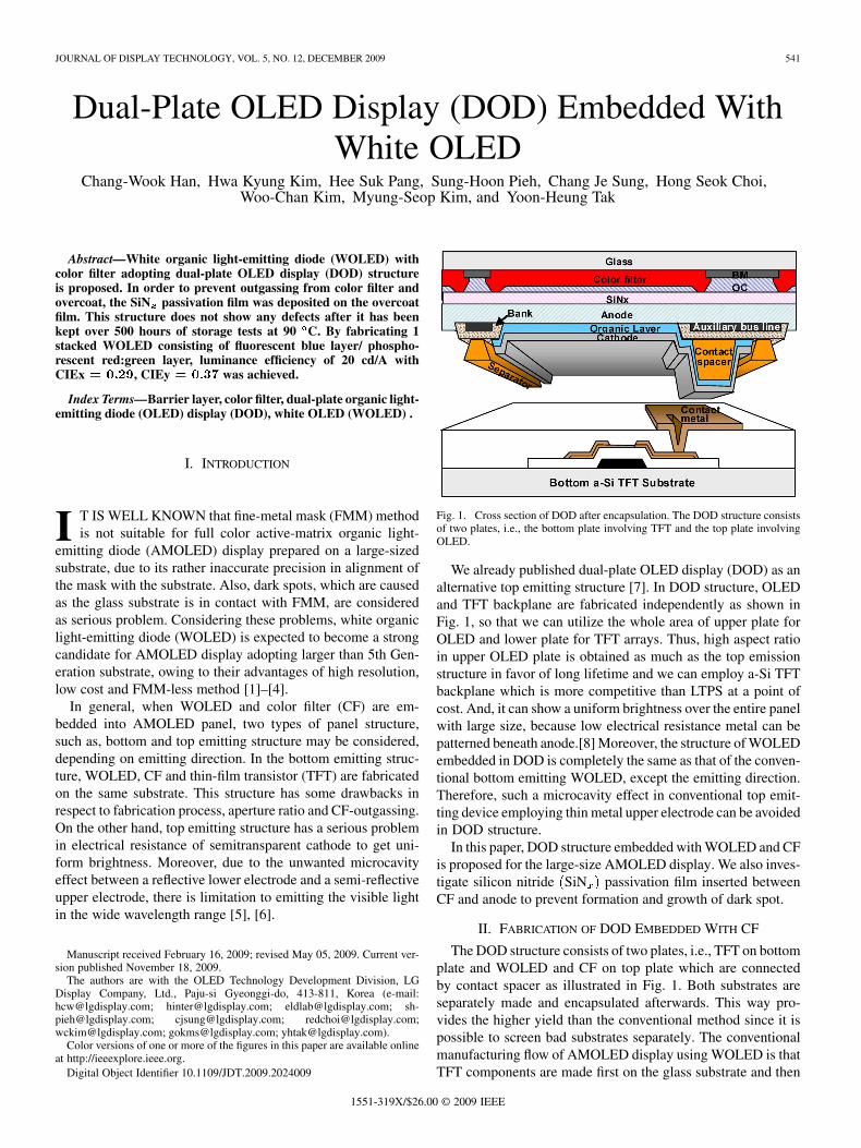
Fig. 1. Cross section of DOD after encapsulation. The DOD structure consistsof two plates, i.e., the bottom plate involving TFT and the top plate involvingOLED.
We already published dual-plate OLED display (DOD) as analternative top emitting structure [7]. In DOD structure, OLEDand TFT backplane are fabricated independently as shown inFig. 1, so that we can utilize the whole area of upper plate forOLED and lower plate for TFT arrays. Thus, high aspect ratioin upper OLED plate is obtained as much as the top emissionstructure in favor of long lifetime and we can employ a-Si TFTbackplane which is more competitive than LTPS at a point ofcost. And, it can show a uniform brightness over the entire panelwith large size, because low electrical resistance metal can bepatterned beneath anode.[8] Moreover, the structure of WOLEDembedded in DOD is completely the same as that of the conven-tional bottom emitting WOLED, except the emitting direction.Therefore, such a microcavity effect in conventional top emit-ting device employing thin metal upper electrode can be avoidedin DOD structure.
In this paper, DOD structure embedded with WOLED and CFis proposed for the large-size AMOLED display. We also inves-tigate silicon nitride SiN passivation film inserted betweenCF and anode to prevent formation and growth of dark spot.
II. FABRICATION OF DOD EMBEDDED WITH CF
The DOD structure consists of two plates, i.e., TFT on bottomplate and WOLED and CF on top plate which are connectedby contact spacer as illustrated in Fig. 1. Both substrates areseparately made and encapsulated afterwards. This way pro-vides the higher yield than the conventional method since it ispossible to screen bad substrates separately. The conventionalmanufacturing flow of AMOLED display using WOLED is thatTFT components are made first on the glass substrate and then
1551-319X/$26.00 © 2009 IEEE
542 JOURNAL OF DISPLAY TECHNOLOGY, VOL. 5, NO. 12, DECEMBER 2009
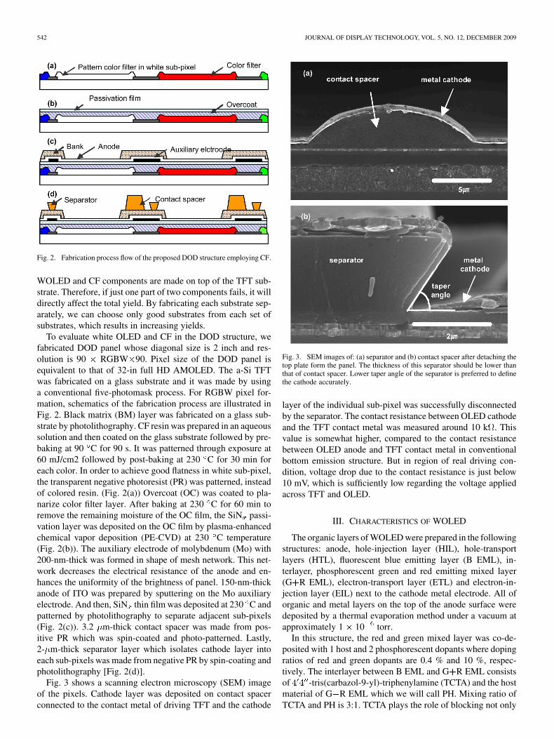
Fig. 2. Fabrication process flow of the proposed DOD structure employing CF.
WOLED and CF components are made on top of the TFT sub-strate. Therefore, if just one part of two components fails, it willdirectly affect the total yield. By fabricating each substrate sep-arately, we can choose only good substrates from each set ofsubstrates, which results in increasing yields.
To evaluate white OLED and CF in the DOD structure, wefabricated DOD panel whose diagonal size is 2 inch and res-olution is 90 RGBW 90. Pixel size of the DOD panel isequivalent to that of 32-in full HD AMOLED. The a-Si TFTwas fabricated on a glass substrate and it was made by usinga conventional five-photomask process. For RGBW pixel for-mation, schematics of the fabrication process are illustrated inFig. 2. Black matrix (BM) layer was fabricated on a glass sub-strate by photolithography. CF resin was prepared in an aqueoussolution and then coated on the glass substrate followed by pre-baking at 90 C for 90 s. It was patterned through exposure at60 mJ/cm2 followed by post-baking at 230 C for 30 min foreach color. In order to achieve good flatness in white sub-pixel,the transparent negative photoresist (PR) was patterned, insteadof colored resin. (Fig. 2(a)) Overcoat (OC) was coated to pla-narize color filter layer. After baking at 230 C for 60 min toremove the remaining moisture of the OC film, the SiN passi-vation layer was deposited on the OC film by plasma-enhancedchemical vapor deposition (PE-CVD) at 230 C temperature(Fig. 2(b)). The auxiliary electrode of molybdenum (Mo) with200-nm-thick was formed in shape of mesh network. This net-work decreases the electrical resistance of the anode and en-hances the uniformity of the brightness of panel. 150-nm-thickanode of ITO was prepared by sputtering on the Mo auxiliaryelectrode. And then, SiN thin film was deposited at 230 C andpatterned by photolithography to separate adjacent sub-pixels(Fig. 2(c)). 3.2 m-thick contact spacer was made from pos-itive PR which was spin-coated and photo-patterned. Lastly,2- m-thick separator layer which isolates cathode layer intoeach sub-pixels was made from negative PR by spin-coating andphotolithography [Fig. 2(d)].
Fig. 3 shows a scanning electron microscopy (SEM) imageof the pixels. Cathode layer was deposited on contact spacerconnected to the contact metal of driving TFT and the cathode
Fig. 3. SEM images of: (a) separator and (b) contact spacer after detaching thetop plate form the panel. The thickness of this separator should be lower thanthat of contact spacer. Lower taper angle of the separator is preferred to definethe cathode accurately.
layer of the individual sub-pixel was successfully disconnectedby the separator. The contact resistance between OLED cathodeand the TFT contact metal was measured around 10 k . Thisvalue is somewhat higher, compared to the contact resistancebetween OLED anode and TFT contact metal in conventionalbottom emission structure. But in region of real driving con-dition, voltage drop due to the contact resistance is just below10 mV, which is sufficiently low regarding the voltage appliedacross TFT and OLED.
III. CHARACTERISTICS OF WOLED
The organic layers of WOLED were prepared in the followingstructures: anode, hole-injection layer (HIL), hole-transportlayers (HTL), fluorescent blue emitting layer (B EML), in-terlayer, phosphorescent green and red emitting mixed layer(G R EML), electron-transport layer (ETL) and electron-in-jection layer (EIL) next to the cathode metal electrode. All oforganic and metal layers on the top of the anode surface weredeposited by a thermal evaporation method under a vacuum atapproximately 1 10 torr.
In this structure, the red and green mixed layer was co-de-posited with 1 host and 2 phosphorescent dopants where dopingratios of red and green dopants are 0.4 % and 10 %, respec-tively. The interlayer between B EML and G R EML consistsof -tris(carbazol-9-yl)-triphenylamine (TCTA) and the hostmaterial of G R EML which we will call PH. Mixing ratio ofTCTA and PH is 3:1. TCTA plays the role of blocking not only
HAN et al.: DUAL-PLATE OLED DISPLAY EMBEDDED WITH WOLED 543
Fig. 4. Electroluminescent spectra of WOLED with red doping ratios of 0.2%(dashed line) and 0.4% (solid line), in which thickness of HIL is 500 ��. (inset:device structure of WOLED).
electron transfer but also triplet-exciton from the phosphores-cent emitting layer (G R EML) to the fluorescent emitting layer(B EML), due to its high LUMO level and triplet energy level.In case that the interlayer consists of TCTA only, the electronblocking property is so strong that electron–hole recombinationoccurs mostly at G R EML and WOLED emits weak blue light.As mixing PH into the interlayer, electrons are transferred fromG R EML to B EML so that electron–hole recombination oc-curs at B EML as well. It is found that our WOLED shows op-timal white color at the mixing ratio of 3:1.
Before fabricating entire WOLED, we studied to find the op-timum concentration of the dopants in G R EML for improvingefficiency and color tunability. When green and red dopants are10% and 0.4%, respectively, we found that the WOLED showsthe best result. Although amount of red dopant is quite small,Fig. 4 shows that intensity of red region in white spectrum isconsiderable. These phenomena can be explained by the excitonenergy transfer from green dopant to red dopant. In other words,green dopant acts as the host of red dopant. It was confirmedby the fact that intensity of red region is enhanced as the greendopant increases [9].
Fig. 4 displays the electroluminescent spectra of the WOLEDof red dopant with 0.2% and 0.4% respectively, with greendopant kept at 10% and 500 -thick HTL in both devices.As amount of red dopant is raised, intensity of red region isincreased, but that of green is decreased. It means that moreexciton energy transfer occurs from green dopant to red dopantin G R EML. The WOLED with 0.4% red doping ratio showsefficiency of 18.7 cd/A and CIEx , CIEy at 3.9mA cm . For 0.2% red doping ratio, the efficiency is 20 cd/Awith CIEx , CIEy at the same current density.
IV. 2-IN DOD PANEL EMBEDDED WITH WOLED AND CF
A. Optimization of WOLED in DOD Panel
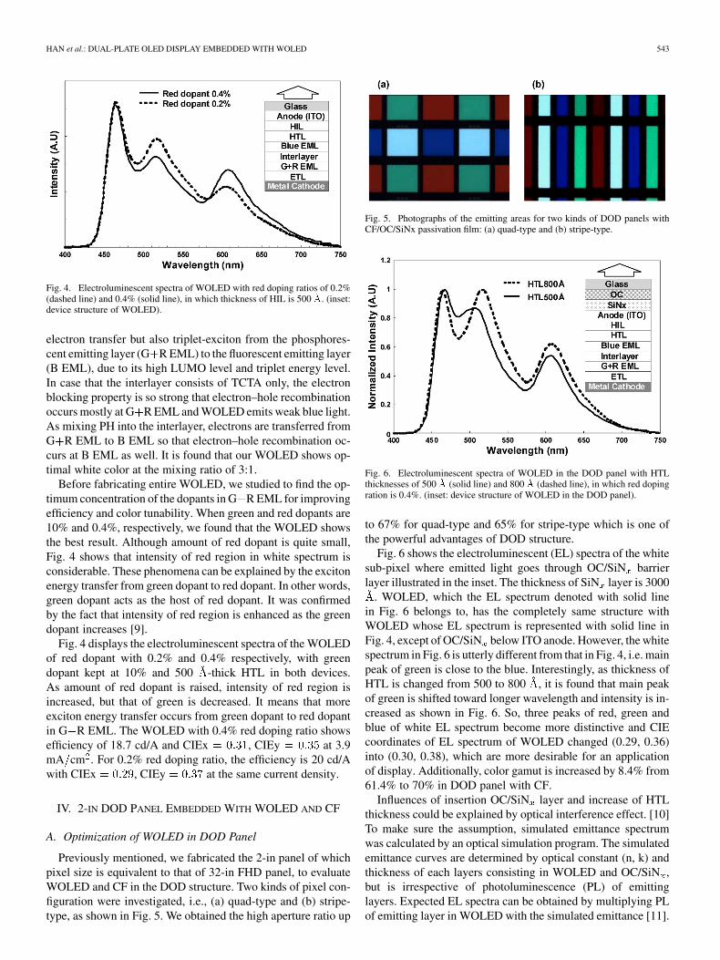
Previously mentioned, we fabricated the 2-in panel of whichpixel size is equivalent to that of 32-in FHD panel, to evaluateWOLED and CF in the DOD structure. Two kinds of pixel con-figuration were investigated, i.e., (a) quad-type and (b) stripe-type, as shown in Fig. 5. We obtained the high aperture ratio up
Fig. 5. Photographs of the emitting areas for two kinds of DOD panels withCF/OC/SiNx passivation film: (a) quad-type and (b) stripe-type.
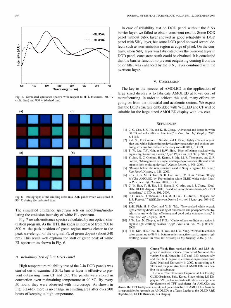
Fig. 6. Electroluminescent spectra of WOLED in the DOD panel with HTLthicknesses of 500 �� (solid line) and 800 �� (dashed line), in which red dopingration is 0.4%. (inset: device structure of WOLED in the DOD panel).
to 67% for quad-type and 65% for stripe-type which is one ofthe powerful advantages of DOD structure.
Fig. 6 shows the electroluminescent (EL) spectra of the whitesub-pixel where emitted light goes through OC/SiN barrierlayer illustrated in the inset. The thickness of SiN layer is 3000
. WOLED, which the EL spectrum denoted with solid linein Fig. 6 belongs to, has the completely same structure withWOLED whose EL spectrum is represented with solid line inFig. 4, except of OC/SiN below ITO anode. However, the whitespectrum in Fig. 6 is utterly different from that in Fig. 4, i.e. mainpeak of green is close to the blue. Interestingly, as thickness ofHTL is changed from 500 to 800 , it is found that main peakof green is shifted toward longer wavelength and intensity is in-creased as shown in Fig. 6. So, three peaks of red, green andblue of white EL spectrum become more distinctive and CIEcoordinates of EL spectrum of WOLED changed (0.29, 0.36)into (0.30, 0.38), which are more desirable for an applicationof display. Additionally, color gamut is increased by 8.4% from61.4% to 70% in DOD panel with CF.
Influences of insertion OC/SiN layer and increase of HTLthickness could be explained by optical interference effect. [10]To make sure the assumption, simulated emittance spectrumwas calculated by an optical simulation program. The simulatedemittance curves are determined by optical constant (n, k) andthickness of each layers consisting in WOLED and OC/SiN ,but is irrespective of photoluminescence (PL) of emittinglayers. Expected EL spectra can be obtained by multiplying PLof emitting layer in WOLED with the simulated emittance [11].
544 JOURNAL OF DISPLAY TECHNOLOGY, VOL. 5, NO. 12, DECEMBER 2009
Fig. 7. Simulated emittance spectra with respect to HTL thickness; 500 ��(solid line) and 800 �� (dashed line).
Fig. 8. Photographs of the emitting areas in a DOD panel which was stored at90 C during the indicated time.
The simulated emittance spectrum acts on modifying/modu-lating the emission intensity of white EL spectrum.
Fig. 7 reveals emittance spectra calculated by our optical sim-ulation program. As the HTL thickness is increased from 500 to800 , the peak position of green region moves closer to thepeak wavelength of the original PL of green dopant (about 540nm). This result well explains the shift of green peak of whiteEL spectrum as shown in Fig. 6.
B. Reliability Test of 2-in DOD Panel
High temperature reliability test of the 2-in DOD panels wascarried out to examine if SiNx barrier layer is effective to pre-vent outgassing from CF and OC. The panels were stored inconvection oven maintaining temperature at 90 C. By every50 hours, they were observed with microscope. As shown inFig. 8(a)-(d), there is no change in emitting area after over 500hours of keeping at high temperature.
In case of reliability test on DOD panel without the SiNxbarrier layer, we failed to obtain consistent results. Some DODpanel without SiNx layer showed as good reliability as DODpanel with SiN layer, but some DOD panel showed several de-fects such as non-emission region at edge of pixel. On the con-trary, when SiN layer was fabricated over the overcoat layer inDOD panel, consistent result could be obtained. It is concludedthat the barrier function to prevent outgassing coming from thecolor filter was enhanced by the SiN layer combined with theovercoat layer.
V. CONCLUSION
The key to the success of AMOLED in the application oflarge sized display is to fabricate AMOLED at lower cost ofmanufacturing. In order to achieve this goal, many efforts aregoing on from the industrial and academic sectors. We expectthat the DOD structure embedded with WOLED and CF will besuitable for the large-sized AMOLED display with low cost.
REFERENCES
[1] C. C. Chu, J. K. Ha, and K. H. Cjung, “Advanced and issues in whiteOLED and color filter architecture,” in Proc. Soc. Inf. Display, 2007,p. 1118.
[2] S.-J. Su, E. Gonmori, J. Sasabe, and J. Kido, Highly efficient organicblue-and white-light emitting devices having a carier-and exciton-con-fining structure for reduced efficiency roll-off 2008, p. 4189.
[3] T.-W. Lee, T.Y. Noh, and D.W. Shin, “High-efficiency stacked whiteorganic light-emitting diodes,” Appl. Phys. Lett., vol. 92, p. 5071, 2003.
[4] Y. Sun, N. C. Giebink, H. Kanno, B. Ma, M. E. Thompson, and S. R.Forrest, “Management of singlet and triplet excitons for efficient whiteorganic light-emitting devices,” Nature Letters, p. 908, 2006.
[5] “Reason behind the new structure used in Sony’s organic EL panel,”Flat Panel Display, p. 128, 2005.
[6] S. Y. Kim, M. G. Kim, S. H. Lee, and J. M. Kim, “3.0-in 308-ppiWVGA AMOLED by Top-emitting white OLED white color filter,”in Proc. Soc. Inf. Display, 2008, p. 937.
[7] C.-W. Han, Y.-H. Tak, I. B. Kang, B.-C. Ahn, and I. J. Cjung, “Dual-plate OLED display (DOD) based on amorphous-silicon(a-Si) TFTbackplane,” J. SID, p. 101, 2009.
[8] C. C. Wu, S. D. Theiuss, G. Gu, M. H. Lu, J. C. Sturm, S. Wagner, andS. R. Forrest, “,” IEEE Electron Device Lett., vol. 18, no. , pp. 609–612,1997.
[9] S.-H. Pieh, H. S. Choi, and Y. H. Tak, “Two-stacked white organiclight-emitting diodes consisting of fluorescent and phosphorescent hy-brid structure with high efficiency and good color characteristics,” inProc. Soc. Inf. Display, 2009.
[10] J. W. Lee, N. Chopra, and F. So, “Cavity effects on light extraction inorganic light emitting devices,” Appl. Phys. Lett., vol. 92, p. 033303,2008.
[11] H. K. Kim, H. S. Choi, D. H. You, and J. W. Yang, “Method to enhancecolor gamut up to 89% in bottom emission active-matrix organic lightemitting device,” in Proc. Int. Meeting on Inf. Display, 2007, p. 43.
Chang-Wook Han received the B.S. and M.S. de-grees in material science from Seoul National Uni-versity, Seoul, Korea, in 1987 and 1989, respectively,and the Ph.D. degree in electrical engineering fromSeoul National University in 2007, researching a-SiTFTs and the pixel structure of AMOLEDs on a flex-ible metal substrate.
He is a Chief Research Engineer at LG Display,OLED Business, Paju, Korea. Since joining LG Dis-play in 1990, he has worked on the device and processdevelopment of TFT backplanes for AMLCDs and
also on the TFT backplane, circuit, and panel structure of AMOLEDs. Now, heis responsible for research on AMOLEDs as a Team Leader at the OLED R&DDepartment, OLED Business, LG Display.
HAN et al.: DUAL-PLATE OLED DISPLAY EMBEDDED WITH WOLED 545
Hwa-Kyung Kim received the B.S. and M.S. degreesin material science engineering from Hanyang Uni-versity and Pohang University for Science and Tech-nology (POSTECH), respectively.
She is a Research Engineer at LG Display, OLEDBusiness, Paju, Korea. Since joining LG ElectronicsCompany in 2004, she has worked on the device de-velopment for AMOLED. Now, she is responsible forresearch on WOLED and CF as research engineerat OLED Technology Development Team 1, OLEDBusiness, LG Display.
Heesuk Pang received the M.S. degree in physicsfrom Sungkyunkwan University. Seoul, Korea, inwhich year??
He is an Senior Research Engineer at the LGDisplay, OLED Business, Paju, Korea. He is respon-sible for the research and development of AMOLEDdisplays. He joined LG Display in 2000, he hasworked on process development of TFT back planefor AMOLED as a process engineer. Now He isdeveloping the new structure and process for largesize AMOLED.
Sung-Hoon Pieh received the B.S. and M.S. degreesin electrical engineering from Soong-Sil and KoreaUniversity, respectively.
He is a junior Research Engineer at LG Display,OLED Business, Paju, Korea. His M.S. work wason fabrication of Nano Device using selective pat-terning with e-beam Lithography, LCD projectionLithography. Since joining LG Electronics Co. in2005, he has worked on the device development forAMOLED. Now, he is responsible for research onWOLED as research engineer at OLED Technology
Development Team 1, LG Display.
Chang Je Sung is Research Engineer at LG Display,OLED Business, Paju, Korea. received the B.S. andM.S. degrees in Physics from Yonsei University.His work was on carrier injection and transport inOLEDs. In 2004, he joined the LG Electronics Com-pany and since then he worked on the organic devicetechnology and process engineering of AMOLEDdisplay.
Hong Seok Choi received the B.S., M.S., and Ph.D.degrees in physics from Seoul National University,Korea, in 1992, 1994, and 1999, respectively. HisPh.D. work was on optical properties of transitionmetal oxides.
He is a Chief Research Engineer at LG Display,OLED Business, Paju, Korea.In 2001, he joined LGElectronics Company and worked on technical devel-opment of OLED. In 2008, he transferred to LG Dis-play and has researched OLED.
Woo Chan Kim e received the B.S. degrees in met-allurgical engineering from Korea University, Korea,in 1994, and the M.S. and Ph.D. degrees in materialscience from KAIST, Korea, in 1996 and 2002, re-spectively.
He is a Chief Research Engineer at LG Display,OLED Business, Paju, Korea. Since joining LG Dis-play in 2002, he has worked on the process develop-ment and also on panel structure of AMOLED dis-plays.
Myung-Seop Kim received the M.S. degrees inPhysics and the Ph.D. in Applied Physics fromYonsei University, Korea, in 1997 and 2007, respec-tively.
He is a Chief Research Engineer at LG Display,OLED Business, Paju, Korea. Since joining LG Elec-tronics Co. in 1997, he has worked on the develop-ment of AMOLED device. Now, he is researching onthe degradation mechanism of OLED device and isresponsible for process technology of AMOLED dis-plays at OLED Business, LG Display.
Yoon-Heung Tak received the B.S. degree in chem-istry and M.S. degree and his Ph.D. in physical chem-istry from Philips Marburg University, Germany, in1991, 1994, and 1997, respectively. His Ph.D. workwas on the injection, transport, and recombination ofcharge carriers in OLEDs.
He is a Vice President at LG Display, OLEDBusiness, Gumi, Korea. He is responsible for theprocess and production department of AMOLEDdisplays. In 1997, he joined the LG Electronics Co.and since then he has worked on the technology,
process, and product development of AMOLED displays. He is currently theHead of the OLED Process & Production Department, OLED Business, LGDisplay.