Embed Size (px)
Citation preview
Copyright ©2016 DENSITRON TECHNOLOGIES Ltd. All rights reserved. – Proprietary Data
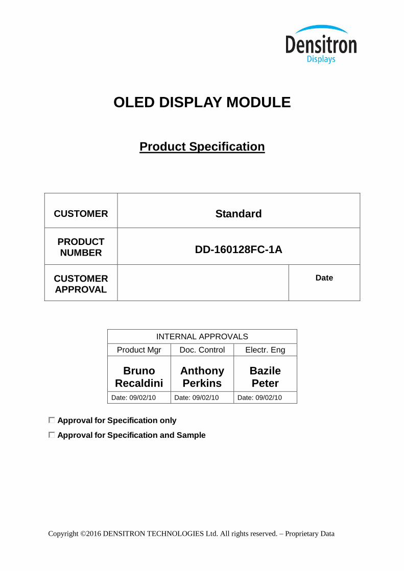
OLED DISPLAY MODULE
Product Specification
CUSTOMER Standard
PRODUCT NUMBER DD-160128FC-1A
CUSTOMER APPROVAL
Date
INTERNAL APPROVALS
Product Mgr Doc. Control Electr. Eng
Bruno Recaldini
Anthony Perkins
Bazile Peter
Date: 09/02/10 Date: 09/02/10 Date: 09/02/10
Approval for Specification only
Approval for Specification and Sample
Product No. DD-160128FC-1A REV. C
Page 2 / 29
Copyright ©2016 DENSITRON TECHNOLOGIES Ltd. All rights reserved. – Proprietary Data
TABLE OF CONTENTS
1 MAIN FEATURES .......................................................................................................... 4
2 MECHANICAL SPECIFICATION ............................................................................... 5
2.1 MECHANICAL CHARACTERISTICS .................................................................... 5 2.2 MECHANICAL DRAWING ..................................................................................... 6
3 ELECTRICAL SPECIFICATION ................................................................................. 7
3.1 ABSOLUTE MAXIMUM RATINGS ....................................................................... 7 3.2 ELECTRICAL CHARACTERISTICS ...................................................................... 8
3.3 INTERFACE PIN ASSIGNMENT ............................................................................ 9 3.4 BLOCK DIAGRAM ................................................................................................ 11
3.5 TIMING CHARACTERISTICS .............................................................................. 12
4 OPTICAL SPECIFICATION ....................................................................................... 18
4.1 OPTICAL CHARACTERISTICS ............................................................................ 18
5 FUNCTIONAL SPECIFICATION .............................................................................. 19
5.1 COMMANDS .......................................................................................................... 19 5.2 POWER UP/DOWN SEQUENCE ........................................................................... 19
5.3 RESET CIRCUIT ..................................................................................................... 19 5.4 ACTUAL APPLICATION EXAMPLE ................................................................... 20
6 PACKAGING AND LABELLING SPECIFICATION .............................................. 21
6.1 LABELLING & MARKING .................................................................................... 21
7 QUALITY ASSURANCE SPECIFICATION ............................................................. 22
7.1 CONFORMITY ....................................................................................................... 22 7.2 DELIVERY ASSURANCE ..................................................................................... 22
7.3 DEALING WITH CUSTOMER COMPLAINTS .................................................... 26
8 RELIABILITY SPECIFICATION .............................................................................. 27
8.1 RELIABILITY TESTS ............................................................................................ 27
8.2 LIFE TIME ............................................................................................................... 27
9 HANDLING PRECAUTIONS ...................................................................................... 28
10 SUPPORTED ACCESSORIES .................................................................................... 29
10.1 DUO KIT .................................................................................................................. 29
10.2 TRANSITION BOARD CARD ............................................................................... 29 10.3 CONNECTOR BOARD CARD ............................................................................... 29 10.4 CONNECTOR ......................................................................................................... 29
Product No. DD-160128FC-1A REV. C
Page 3 / 29
Copyright ©2016 DENSITRON TECHNOLOGIES Ltd. All rights reserved. – Proprietary Data
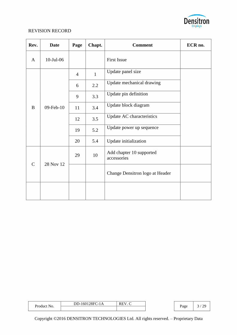
REVISION RECORD
Rev. Date Page Chapt. Comment ECR no.
A 10-Jul-06 First Issue
B 09-Feb-10
4 1 Update panel size
6 2.2 Update mechanical drawing
9 3.3 Update pin definition
11 3.4 Update block diagram
12 3.5 Update AC characteristics
19 5.2 Update power up sequence
20 5.4 Update initialization
C 28 Nov 12
29 10 Add chapter 10 supported
accessories
Change Densitron logo at Header
Product No. DD-160128FC-1A REV. C
Page 4 / 29
Copyright ©2016 DENSITRON TECHNOLOGIES Ltd. All rights reserved. – Proprietary Data
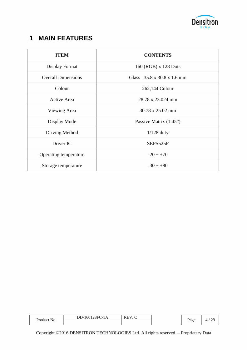
1 MAIN FEATURES
ITEM CONTENTS
Display Format 160 (RGB) x 128 Dots
Overall Dimensions Glass 35.8 x 30.8 x 1.6 mm
Colour 262,144 Colour
Active Area 28.78 x 23.024 mm
Viewing Area 30.78 x 25.02 mm
Display Mode Passive Matrix (1.45”)
Driving Method 1/128 duty
Driver IC SEPS525F
Operating temperature -20 ~ +70
Storage temperature -30 ~ +80

Product No. DD-160128FC-1A REV. C
Page 5 / 29
Copyright ©2016 DENSITRON TECHNOLOGIES Ltd. All rights reserved. – Proprietary Data
2 MECHANICAL SPECIFICATION
2.1 MECHANICAL CHARACTERISTICS
ITEM CHARACTERISTIC UNIT
Display Format 160 (RGB) x 128 Dots
Overall Dimensions 35.80 x 30.80 x 1.6 mm
Viewing Area 30.78 x 25.02 mm
Active Area 28.78 x 23.024 mm
Dot Size 0.04 x 0.164 mm
Dot Pitch 0.06 x 0.18 mm
Weight 3.6 g
IC Controller/Driver SEPS525F (COF)
Product No. DD-160128FC-1A REV. C
Page 6 / 29
Copyright ©2016 DENSITRON TECHNOLOGIES Ltd. All rights reserved. – Proprietary Data
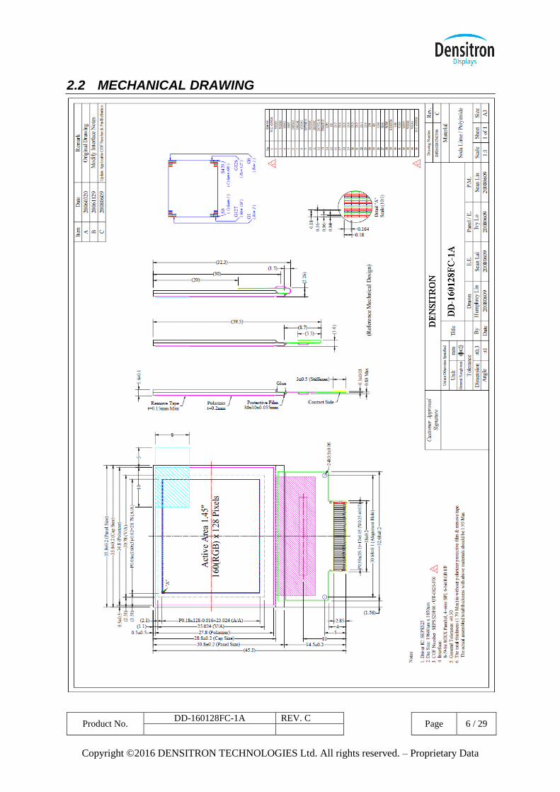
2.2 MECHANICAL DRAWING
Product No. DD-160128FC-1A REV. C
Page 7 / 29
Copyright ©2016 DENSITRON TECHNOLOGIES Ltd. All rights reserved. – Proprietary Data
3 ELECTRICAL SPECIFICATION
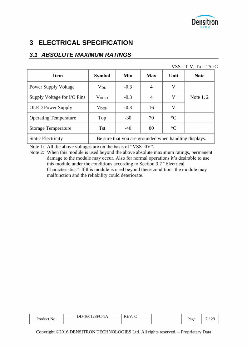
3.1 ABSOLUTE MAXIMUM RATINGS
VSS = 0 V, Ta = 25 °C
Item Symbol Min Max Unit Note
Power Supply Voltage VDD -0.3 4 V
Note 1, 2 Supply Voltage for I/O Pins VDDIO -0.3 4 V
OLED Power Supply VDDH -0.3 16 V
Operating Temperature Top -30 70 °C
Storage Temperature Tst -40 80 °C
Static Electricity Be sure that you are grounded when handling displays.
Note 1: All the above voltages are on the basis of “VSS=0V”.
Note 2: When this module is used beyond the above absolute maximum ratings, permanent
damage to the module may occur. Also for normal operations it’s desirable to use
this module under the conditions according to Section 3.2 “Electrical
Characteristics”. If this module is used beyond these conditions the module may
malfunction and the reliability could deteriorate.
Product No. DD-160128FC-1A REV. C
Page 8 / 29
Copyright ©2016 DENSITRON TECHNOLOGIES Ltd. All rights reserved. – Proprietary Data
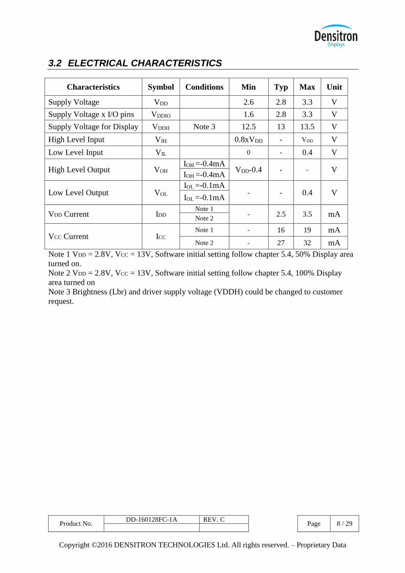
3.2 ELECTRICAL CHARACTERISTICS
Characteristics Symbol Conditions Min Typ Max Unit
Supply Voltage VDD 2.6 2.8 3.3 V
Supply Voltage x I/O pins VDDIO 1.6 2.8 3.3 V
Supply Voltage for Display VDDH Note 3 12.5 13 13.5 V
High Level Input VIH 0.8xVDD - VDD V
Low Level Input VIL 0 - 0.4 V
High Level Output VOH IOH =-0.4mA
VDD-0.4 - - V IOH =-0.4mA
Low Level Output VOL IOL =-0.1mA
- - 0.4 V IOL =-0.1mA
VDD Current IDD Note 1
- 2.5 3.5 mA Note 2
VCC Current ICC Note 1 - 16 19 mA
Note 2 - 27 32 mA
Note 1 VDD = 2.8V, VCC = 13V, Software initial setting follow chapter 5.4, 50% Display area
turned on.
Note 2 VDD = 2.8V, VCC = 13V, Software initial setting follow chapter 5.4, 100% Display
area turned on
Note 3 Brightness (Lbr) and driver supply voltage (VDDH) could be changed to customer
request.
Product No. DD-160128FC-1A REV. C
Page 9 / 29
Copyright ©2016 DENSITRON TECHNOLOGIES Ltd. All rights reserved. – Proprietary Data
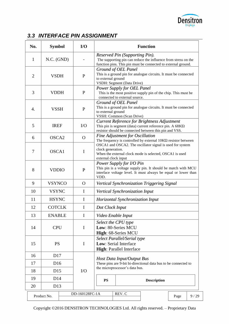
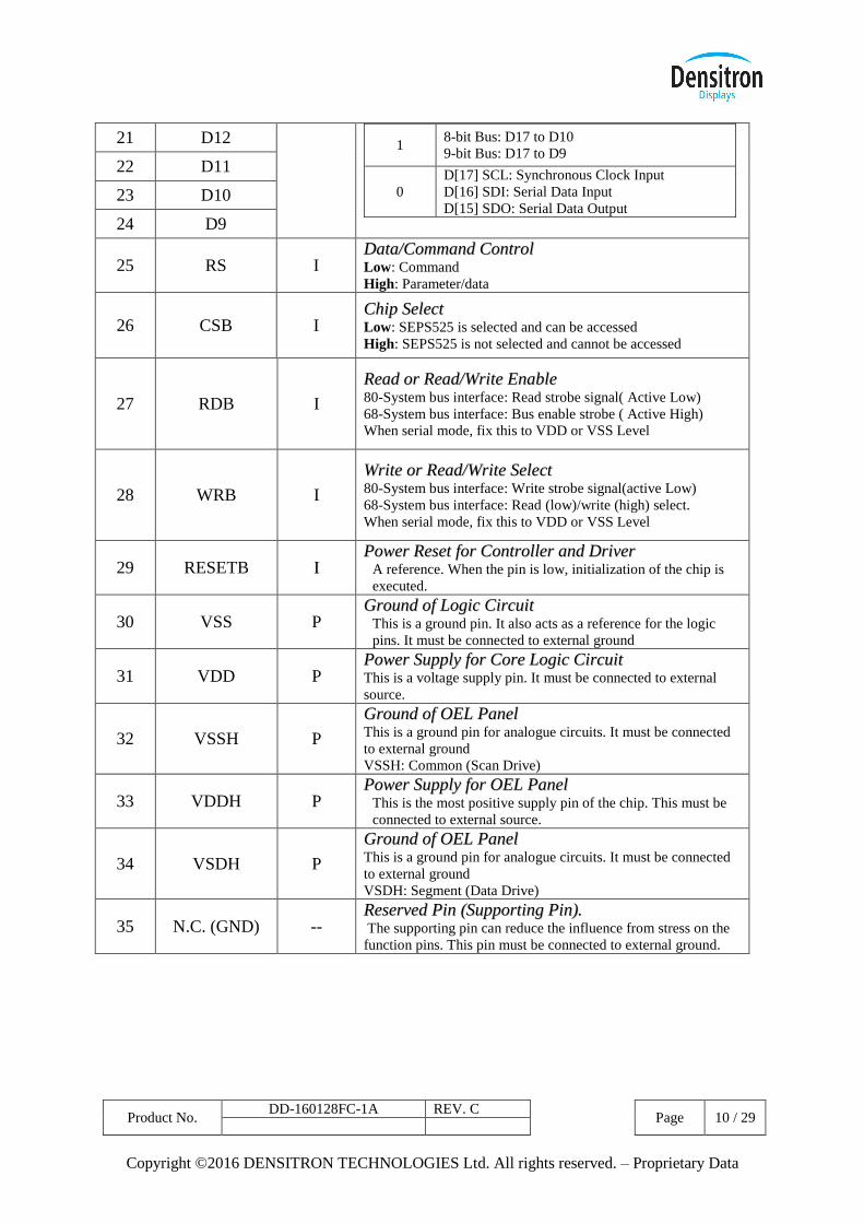
3.3 INTERFACE PIN ASSIGNMENT
No. Symbol I/O Function
1 N.C. (GND) - RReesseerrvveedd PPiinn ((SSuuppppoorrttiinngg PPiinn)).. The supporting pin can reduce the influence from stress on the
function pins. This pin must be connected to external ground.
2 VSDH P
GGrroouunndd ooff OOEELL PPaanneell This is a ground pin for analogue circuits. It must be connected
to external ground
VSDH: Segment (Data Drive)
3 VDDH P PPoowweerr SSuuppppllyy ffoorr OOEELL PPaanneell
This is the most positive supply pin of the chip. This must be
connected to external source.
4. VSSH P
GGrroouunndd ooff OOEELL PPaanneell This is a ground pin for analogue circuits. It must be connected
to external ground
VSSH: Common (Scan Drive)
5 IREF I/O CCuurrrreenntt RReeffeerreennccee ffoorr BBrriigghhttnneessss AAddjjuussttmmeenntt This pin is segment (data) current reference pin. A 68KΏ resistor should be connected between this pin and VSS.
6 OSCA2 O FFiinnee AAddjjuussttmmeenntt ffoorr OOsscciillllaattiioonn The frequency is controlled by external 10KΏ resistor between
OSCA1 and OSCA2. The oscillator signal is used for system
clock generation.
When the external clock mode is selected, OSCA1 is used
external clock input
7 OSCA1 I
8 VDDIO PP
PPoowweerr SSuuppppllyy ffoorr II//OO PPiinn This pin is a voltage supply pin. It should be match with MCU
interface voltage level. It must always be equal or lower than
VDD.
9 VSYNCO O VVeerrttiiccaall SSyynncchhrroonniizzaattiioonn TTrriiggggeerriinngg SSiiggnnaall
10 VSYNC I VVeerrttiiccaall SSyynncchhrroonniizzaattiioonn IInnppuutt
11 HSYNC I HHoorriizzoonnttaall SSyynncchhrroonniizzaattiioonn IInnppuutt
12 COTCLK I DDoott CClloocckk IInnppuutt
13 ENABLE I VViiddeeoo EEnnaabbllee IInnppuutt
14 CPU I SSeelleecctt tthhee CCPPUU ttyyppee
Low: 80-Series MCU
High: 68-Series MCU
15 PS I SSeelleecctt PPaarraalllleell//SSeerriiaall ttyyppee
Low: Serial Interface
High: Parallel Interface
16 D17
I/O
HHoosstt DDaattaa IInnppuutt//OOuuttppuutt BBuuss These pins are 9-bit bi-directional data bus to be connected to
the microprocessor’s data bus.
PS Description
17 D16
18 D15
19 D14
20 D13
Product No. DD-160128FC-1A REV. C
Page 10 / 29
Copyright ©2016 DENSITRON TECHNOLOGIES Ltd. All rights reserved. – Proprietary Data
21 D12 1
8-bit Bus: D17 to D10
9-bit Bus: D17 to D9
0
D[17] SCL: Synchronous Clock Input
D[16] SDI: Serial Data Input
D[15] SDO: Serial Data Output
22 D11
23 D10
24 D9
25 RS I DDaattaa//CCoommmmaanndd CCoonnttrrooll Low: Command
High: Parameter/data
26 CSB I CChhiipp SSeelleecctt Low: SEPS525 is selected and can be accessed
High: SEPS525 is not selected and cannot be accessed
27 RDB I
RReeaadd oorr RReeaadd//WWrriittee EEnnaabbllee 80-System bus interface: Read strobe signal( Active Low)
68-System bus interface: Bus enable strobe ( Active High)
When serial mode, fix this to VDD or VSS Level
28 WRB I
WWrriittee oorr RReeaadd//WWrriittee SSeelleecctt 80-System bus interface: Write strobe signal(active Low)
68-System bus interface: Read (low)/write (high) select.
When serial mode, fix this to VDD or VSS Level
29 RESETB II PPoowweerr RReesseett ffoorr CCoonnttrroolllleerr aanndd DDrriivveerr
A reference. When the pin is low, initialization of the chip is
executed.
30 VSS P GGrroouunndd ooff LLooggiicc CCiirrccuuiitt
This is a ground pin. It also acts as a reference for the logic
pins. It must be connected to external ground
31 VDD P PPoowweerr SSuuppppllyy ffoorr CCoorree LLooggiicc CCiirrccuuiitt This is a voltage supply pin. It must be connected to external
source.
32 VSSH P
GGrroouunndd ooff OOEELL PPaanneell This is a ground pin for analogue circuits. It must be connected
to external ground
VSSH: Common (Scan Drive)
33 VDDH P PPoowweerr SSuuppppllyy ffoorr OOEELL PPaanneell
This is the most positive supply pin of the chip. This must be
connected to external source.
34 VSDH P
GGrroouunndd ooff OOEELL PPaanneell This is a ground pin for analogue circuits. It must be connected
to external ground
VSDH: Segment (Data Drive)
35 N.C. (GND) -- RReesseerrvveedd PPiinn ((SSuuppppoorrttiinngg PPiinn)).. The supporting pin can reduce the influence from stress on the
function pins. This pin must be connected to external ground.
Product No. DD-160128FC-1A REV. C
Page 11 / 29
Copyright ©2016 DENSITRON TECHNOLOGIES Ltd. All rights reserved. – Proprietary Data
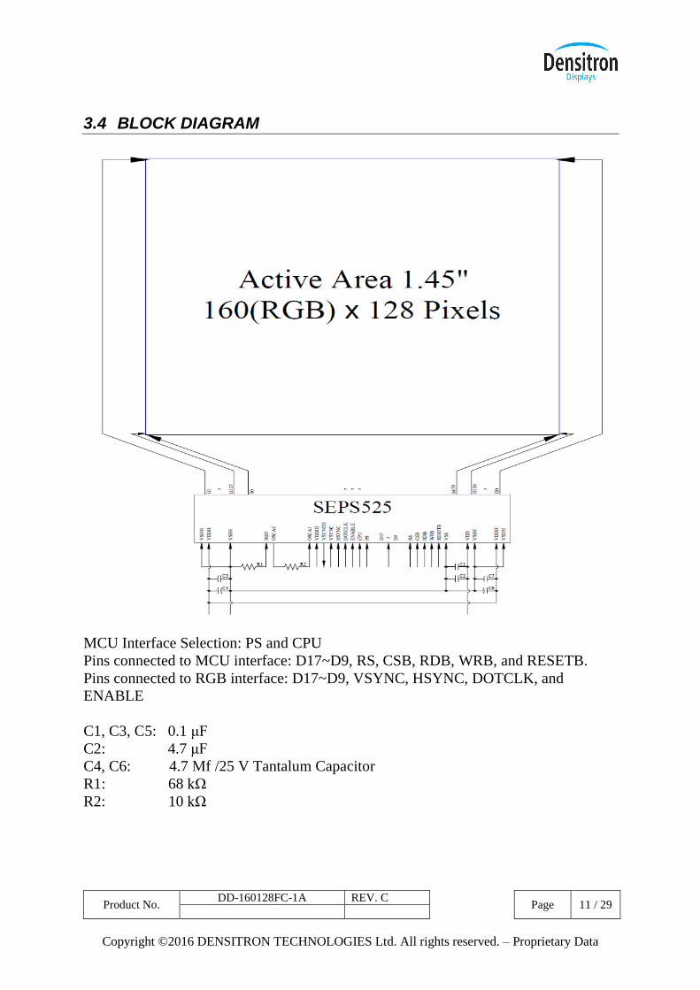
3.4 BLOCK DIAGRAM
MCU Interface Selection: PS and CPU
Pins connected to MCU interface: D17~D9, RS, CSB, RDB, WRB, and RESETB.
Pins connected to RGB interface: D17~D9, VSYNC, HSYNC, DOTCLK, and
ENABLE
C1, C3, C5: 0.1 μF
C2: 4.7 μF
C4, C6: 4.7 Μf /25 V Tantalum Capacitor
R1: 68 kΩ
R2: 10 kΩ
Product No. DD-160128FC-1A REV. C
Page 12 / 29
Copyright ©2016 DENSITRON TECHNOLOGIES Ltd. All rights reserved. – Proprietary Data
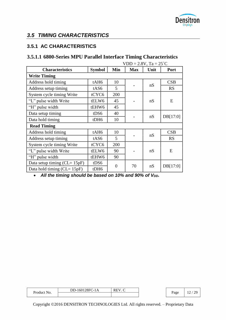
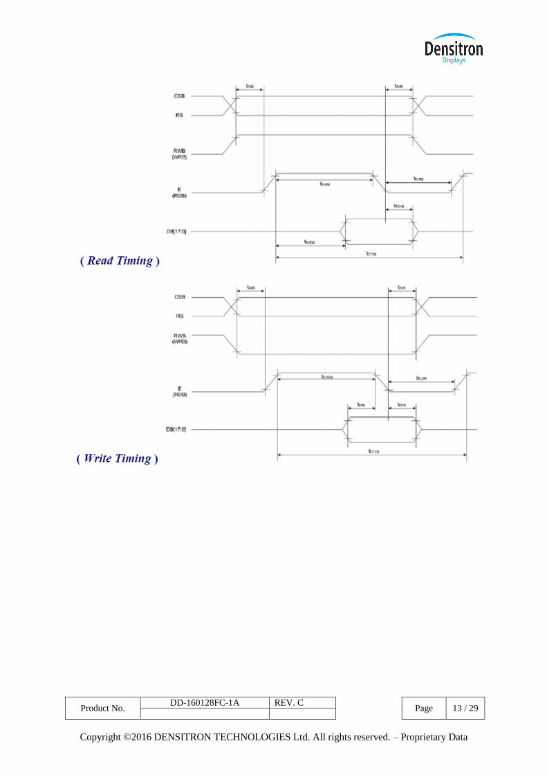
3.5 TIMING CHARACTERISTICS
3.5.1 AC CHARACTERISTICS
3.5.1.1 6800-Series MPU Parallel Interface Timing Characteristics
VDD = 2.8V, Ta = 25˚C
Characteristics Symbol Min Max Unit Port
Write Timing
Address hold timing tAH6 10 - nS
CSB
Address setup timing tAS6 5 RS
System cycle timing Write tCYC6 200
- nS E “L” pulse width Write tELW6 45
“H” pulse width tEHW6 45
Data setup timing tDS6 40 - nS DB[17:0]
Data hold timing tDH6 10
Read Timing
Address hold timing tAH6 10 - nS
CSB
Address setup timing tAS6 5 RS
System cycle timing Write tCYC6 200
- nS E “L” pulse width Write tELW6 90
“H” pulse width tEHW6 90
Data setup timing (CL= 15pF) tDS6 0 70 nS DB[17:0]
Data hold timing (CL= 15pF) tDH6
All the timing should be based on 10% and 90% of VDD.
Product No. DD-160128FC-1A REV. C
Page 13 / 29
Copyright ©2016 DENSITRON TECHNOLOGIES Ltd. All rights reserved. – Proprietary Data
Product No. DD-160128FC-1A REV. C
Page 14 / 29
Copyright ©2016 DENSITRON TECHNOLOGIES Ltd. All rights reserved. – Proprietary Data
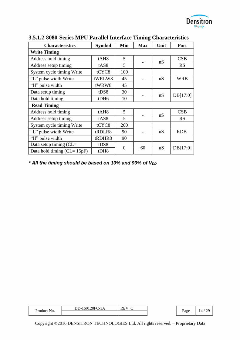
3.5.1.2 8080-Series MPU Parallel Interface Timing Characteristics
Characteristics Symbol Min Max Unit Port
Write Timing
Address hold timing tAH8 5 - nS
CSB
Address setup timing tAS8 5 RS
System cycle timing Write tCYC8 100
- nS WRB “L” pulse width Write tWRLW8 45
“H” pulse width tWRW8 45
Data setup timing tDS8 30 - nS DB[17:0]
Data hold timing tDH6 10
Read Timing
Address hold timing tAH8 5 - nS
CSB
Address setup timing tAS8 5 RS
System cycle timing Write tCYC8 200
- nS RDB “L” pulse width Write tRDLR8 90
“H” pulse width tRDHR8 90
Data setup timing (CL=
15pF) tDS8
0 60 nS DB[17:0] Data hold timing (CL= 15pF) tDH8
* All the timing should be based on 10% and 90% of VDD

Product No. DD-160128FC-1A REV. C
Page 15 / 29
Copyright ©2016 DENSITRON TECHNOLOGIES Ltd. All rights reserved. – Proprietary Data
Product No. DD-160128FC-1A REV. C
Page 16 / 29
Copyright ©2016 DENSITRON TECHNOLOGIES Ltd. All rights reserved. – Proprietary Data
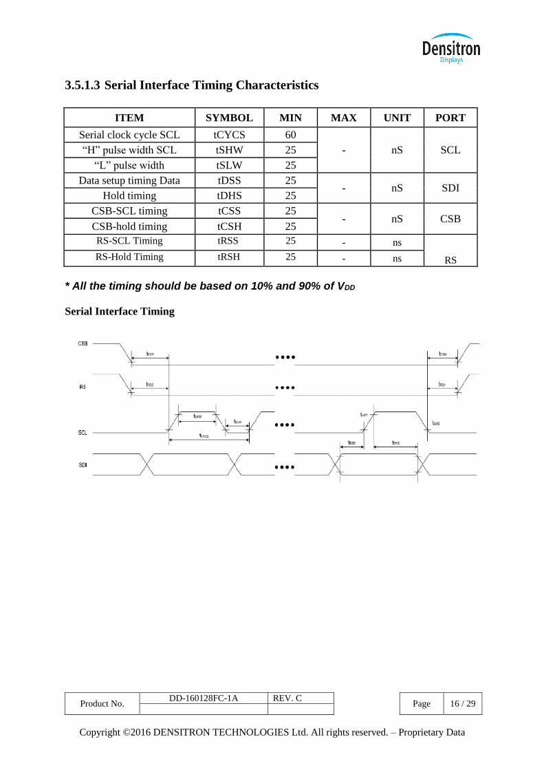
3.5.1.3 Serial Interface Timing Characteristics
ITEM SYMBOL MIN MAX UNIT PORT
Serial clock cycle SCL tCYCS 60
- nS SCL “H” pulse width SCL tSHW 25
“L” pulse width tSLW 25
Data setup timing Data tDSS 25 - nS SDI
Hold timing tDHS 25
CSB-SCL timing tCSS 25 - nS CSB
CSB-hold timing tCSH 25
RS-SCL Timing tRSS 25 - ns
RS RS-Hold Timing tRSH 25 - ns
* All the timing should be based on 10% and 90% of VDD
Serial Interface Timing

Product No. DD-160128FC-1A REV. C
Page 17 / 29
Copyright ©2016 DENSITRON TECHNOLOGIES Ltd. All rights reserved. – Proprietary Data
3.5.1.4 RGB Interface Timing Characteristics
Symbol Item Min Max Unit Port
tDCYC Dot Clock Cycle 100 - ns
tDLW Dot “L” Pulse Width 50 - ns DOTCLK
tDHW Dot “H” Pulse Width 50 - ns
tDS Data Setup Timing 5 --
ns D[17:12]
tDH Data Hold Timing 5 ns
tVLW Vsync Pulse Width 1 - DOTCLK VSYNC
tHLW Hsync Pulse Width 1 - DOTCLK HSYNC
* All the timing should be based on 10% and 90% of VDD
Product No. DD-160128FC-1A REV. C
Page 18 / 29
Copyright ©2016 DENSITRON TECHNOLOGIES Ltd. All rights reserved. – Proprietary Data
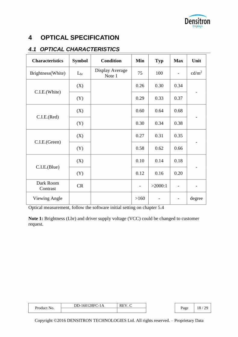
4 OPTICAL SPECIFICATION
4.1 OPTICAL CHARACTERISTICS
Characteristics Symbol Condition Min Typ Max Unit
Brightness(White) Lbr Display Average
Note 1 75 100 - cd/m2
C.I.E.(White)
(X)
0.26 0.30 0.34
-
(Y) 0.29 0.33 0.37
C.I.E.(Red)
(X)
0.60 0.64 0.68
-
(Y) 0.30 0.34 0.38
C.I.E.(Green)
(X)
0.27 0.31 0.35
-
(Y) 0.58 0.62 0.66
C.I.E.(Blue)
(X)
0.10 0.14 0.18
-
(Y) 0.12 0.16 0.20
Dark Room
Contrast CR - >2000:1 - -
Viewing Angle >160 - - degree
Optical measurement, follow the software initial setting on chapter 5.4
Note 1: Brightness (Lbr) and driver supply voltage (VCC) could be changed to customer
request.
Product No. DD-160128FC-1A REV. C
Page 19 / 29
Copyright ©2016 DENSITRON TECHNOLOGIES Ltd. All rights reserved. – Proprietary Data
5 FUNCTIONAL SPECIFICATION
5.1 COMMANDS
Please refer to the Technical Manual for the SEPS525F
5.2 POWER UP/DOWN SEQUENCE
To protect panel and extend the panel lifetime, the driver IC power up/down routine should
include a delay period between high voltage and low voltage power sources during turn
on/off. It gives the panel enough time to complete the action of charge and discharge
before/after the operation.
5.2.1 POWER UP SEQUENCE VDD,, VDDIO ON VDDH ON Display On
1. Power up VDD & VDD IO
2. Send Display off command VDDH
3. Initialization
4. Clear Screen
5. Power up VDDH
6. Delay 100ms (When VDDH is stable) VDD /VDDIO
7. Send Display on command
Ground
5.2.2 POWER DOWN SEQUENCE Display off VDDH off VDD,, VDDIO off
1. Send Display off command
2. Power down VDDH VDDH
3. Delay 100ms
(When VDDH reach 0 and panel is
completely discharges) VDD /VDDIO
4. Power down VDD & VDDIO
Ground
5.3 RESET CIRCUIT
When RESETB input is low, the chip is initialized with the following status: 1. Frame frequency: 90Hz
2. OSC: internal OSC ON
3. DDRAM write horizontal address: MX1 = 00h, MX2 = 9Fh
4. DDRAM write vertical address: MY1 = 00h, MY2 = 7Fh
5. Display data RAM write: HC = 1, VC = 1, HV = 0
6. RGB data swap: OFF
7. Row scan shift direction: G0, G1, … , G126, G127
8. Column data shift direction: S0, S1, … , S478, S479
9. Display ON/OFF: OFF
10. Panel display size: FX1 = 00h, FX2 = 9Fh, FY1 = 00h, FY2 = 7Fh
11. Display data RAM read column/row address: FAC = 00h, FAR = 00h
12. Pre-charge time(R/G/B): 0 clock
13. Pre-charge current(R/G/B): 0 uA
14. Driving current(R/G/B): 0 uA
Product No. DD-160128FC-1A REV. C
Page 20 / 29
Copyright ©2016 DENSITRON TECHNOLOGIES Ltd. All rights reserved. – Proprietary Data
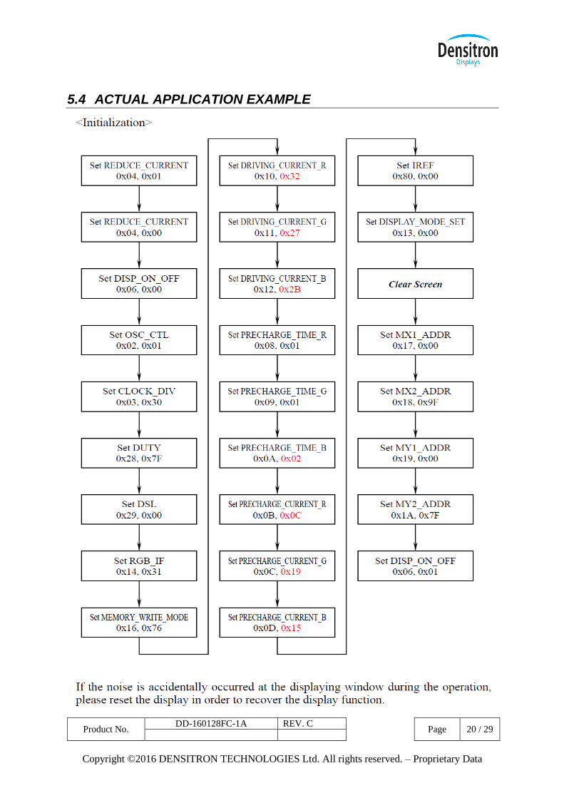
5.4 ACTUAL APPLICATION EXAMPLE
Product No. DD-160128FC-1A REV. C
Page 21 / 29
Copyright ©2016 DENSITRON TECHNOLOGIES Ltd. All rights reserved. – Proprietary Data
6 PACKAGING AND LABELLING SPECIFICATION
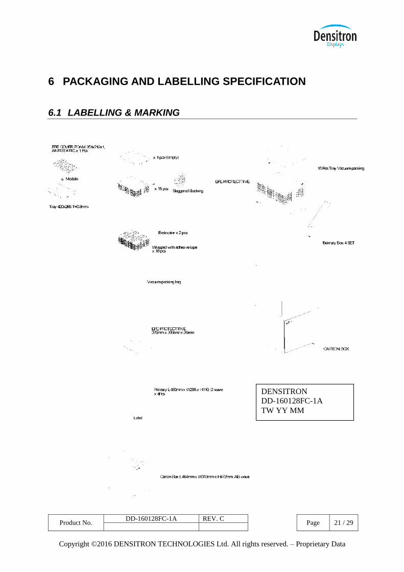
6.1 LABELLING & MARKING
DENSITRON
DD-160128FC-1A
TW YY MM
Product No. DD-160128FC-1A REV. C
Page 22 / 29
Copyright ©2016 DENSITRON TECHNOLOGIES Ltd. All rights reserved. – Proprietary Data
7 QUALITY ASSURANCE SPECIFICATION
7.1 CONFORMITY
The performance, function and reliability of the shipped products conform to the Product
Specification.
7.2 DELIVERY ASSURANCE
7.2.1 DELIVERY INSPECTION STANDARDS
MIL-STD-105E, general inspection level II, single sampling level;
IPC-AA610 rev. C, class 2 electronic assemblies standard
The quality assurance levels are shown below:
Class AQL (%)
Critical defect 0.5%
Major defect 1.0%
Minor defect 1.5%
TOTAL 2.0%
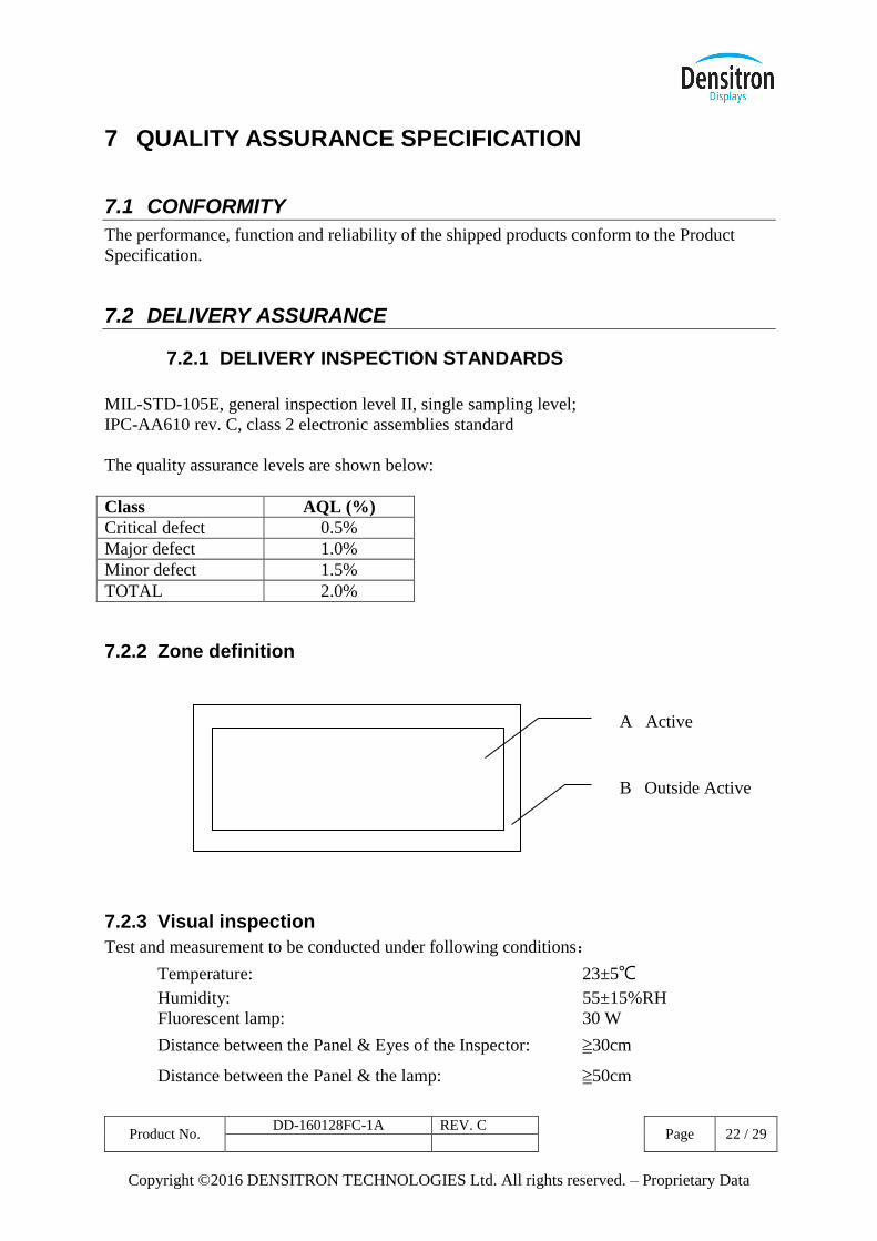
7.2.2 Zone definition
7.2.3 Visual inspection
Test and measurement to be conducted under following conditions:
Temperature: 23±5℃
Humidity: 55±15%RH
Fluorescent lamp: 30 W
Distance between the Panel & Eyes of the Inspector: ≧30cm
Distance between the Panel & the lamp: ≧50cm
A Active
B Outside Active
Product No. DD-160128FC-1A REV. C
Page 23 / 29
Copyright ©2016 DENSITRON TECHNOLOGIES Ltd. All rights reserved. – Proprietary Data
7.2.4 Standard of appearance inspection
Units: mm
Class Item Criteria
Minor Packing &
Label
Outside & inside package Presence of product no., lot no., quantity
Critical Product must not be mixed with others and quantity must not be different from
that indicated on the label
Major Dimension Product dimensions must be according to specification and drawing
Major Electrical Product electrical characteristics must be according to specification
Critical OLED
Display
Missing lines, short circuits or wrong patterns on OLED display are not
allowed
Minor Black spot,
white spot,
dust
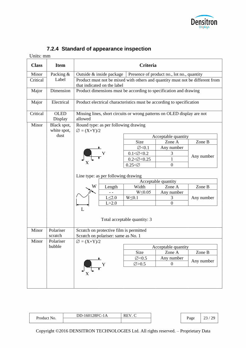
Round type: as per following drawing
= (X+Y)/2
Acceptable quantity
Size Zone A Zone B
<0.1 Any number
Any number
0.1<<0.2 3
0.2<<0.25 1
0.25< 0
Line type: as per following drawing
Acceptable quantity
Length Width Zone A Zone B
- - W≤0.05 Any number
Any number
L≤2.0 W≤0.1 3
L>2.0 0
Total acceptable quantity: 3
Minor Polariser
scratch
Scratch on protective film is permitted
Scratch on polariser: same as No. 1
Minor Polariser
bubble = (X+Y)/2
Acceptable quantity
Size Zone A Zone B
<0.5 Any number Any number
>0.5 0
X
Y
L
W
X
Y
Product No. DD-160128FC-1A REV. C
Page 24 / 29
Copyright ©2016 DENSITRON TECHNOLOGIES Ltd. All rights reserved. – Proprietary Data
Class Item Criteria
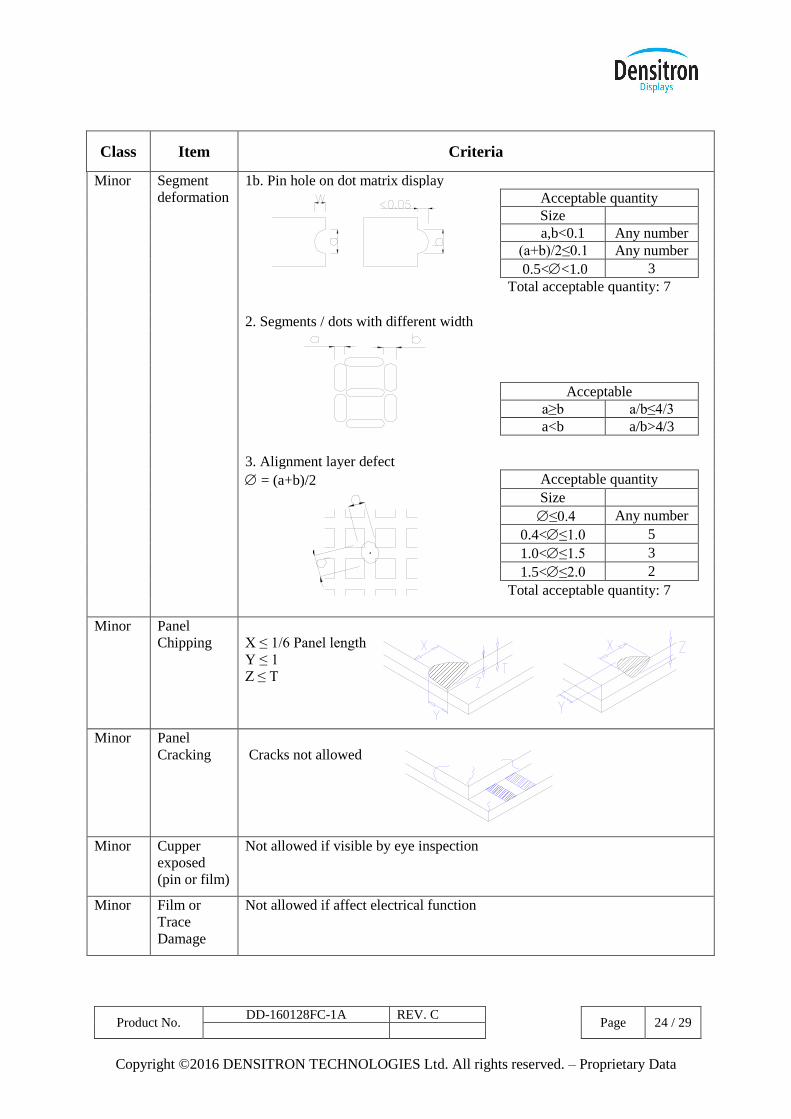
Minor Segment
deformation
1b. Pin hole on dot matrix display
Acceptable quantity
Size
a,b<0.1 Any number
(a+b)/2≤0.1 Any number
0.5<<1.0 3
Total acceptable quantity: 7
2. Segments / dots with different width
Acceptable
a≥b a/b≤4/3
a<b a/b>4/3
3. Alignment layer defect
= (a+b)/2 Acceptable quantity
Size
≤0.4 Any number
0.4<≤1.0 5
1.0<≤1.5 3
1.5<≤2.0 2
Total acceptable quantity: 7
Minor Panel
Chipping
X ≤ 1/6 Panel length
Y ≤ 1
Z ≤ T
Minor Panel
Cracking
Cracks not allowed
Minor Cupper
exposed
(pin or film)
Not allowed if visible by eye inspection
Minor Film or
Trace
Damage
Not allowed if affect electrical function
Product No. DD-160128FC-1A REV. C
Page 25 / 29
Copyright ©2016 DENSITRON TECHNOLOGIES Ltd. All rights reserved. – Proprietary Data
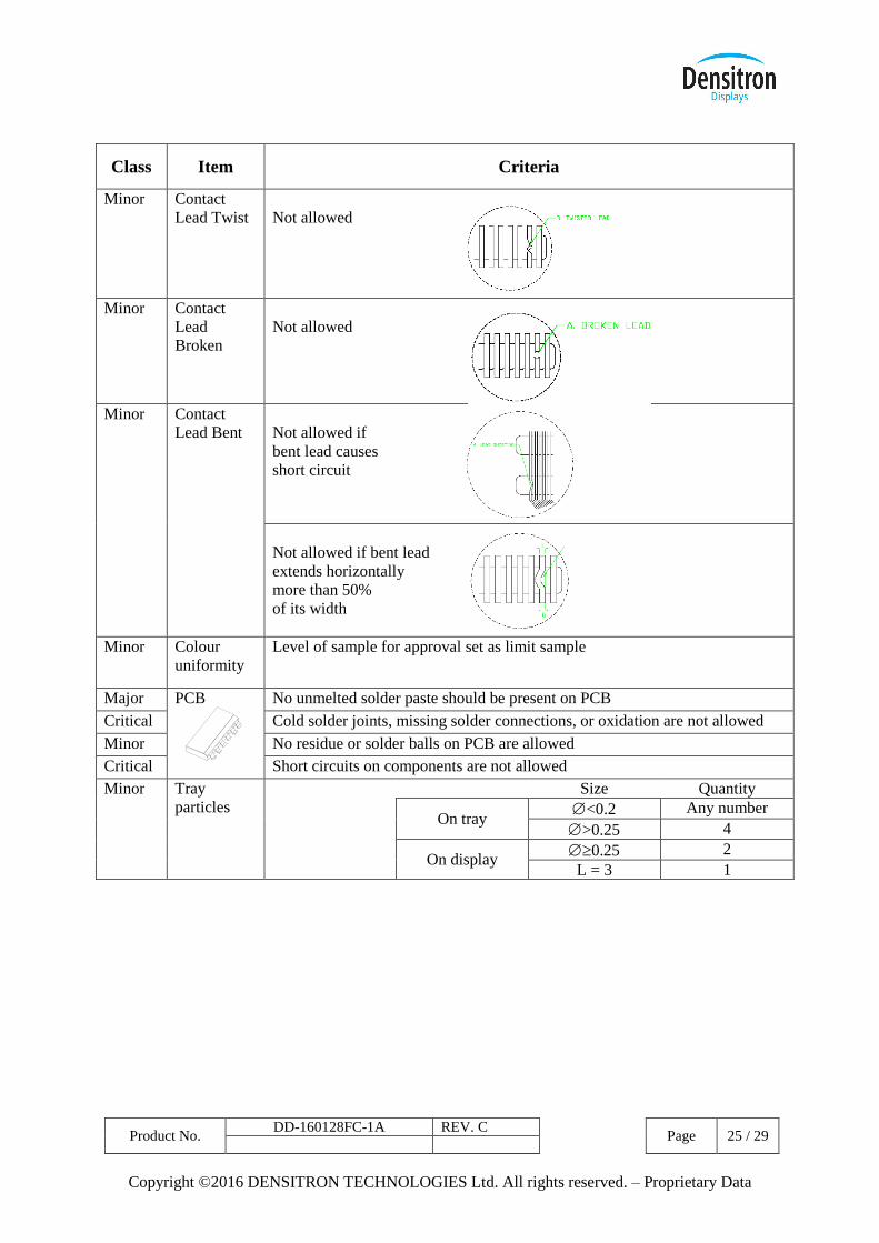
Class Item Criteria
Minor Contact
Lead Twist
Not allowed
Minor Contact
Lead
Broken
Not allowed
Minor Contact
Lead Bent
Not allowed if
bent lead causes
short circuit
Not allowed if bent lead
extends horizontally
more than 50%
of its width
Minor Colour
uniformity
Level of sample for approval set as limit sample
Major PCB
No unmelted solder paste should be present on PCB
Critical Cold solder joints, missing solder connections, or oxidation are not allowed
Minor No residue or solder balls on PCB are allowed
Critical Short circuits on components are not allowed
Minor Tray
particles
Size Quantity
On tray
<0.2 Any number
>0.25 4
On display
0.25 2
L = 3 1
Product No. DD-160128FC-1A REV. C
Page 26 / 29
Copyright ©2016 DENSITRON TECHNOLOGIES Ltd. All rights reserved. – Proprietary Data
7.3 DEALING WITH CUSTOMER COMPLAINTS
7.3.1 Non-conforming analysis
Purchaser should supply Densitron with detailed data of non-conforming sample.
After accepting it, Densitron should complete the analysis in two weeks from receiving the
sample.
If the analysis cannot be completed on time, Densitron must inform the purchaser.
7.3.2 Handling of non-conforming displays
If any non-conforming displays are found during customer acceptance inspection which
Densitron is clearly responsible for, return them to Densitron.
Both Densitron and customer should analyse the reason and discuss the handling of non-
conforming displays when the reason is not clear.
Equally, both sides should discuss and come to agreement for issues pertaining to
modification of Densitron quality assurance standard.
Product No. DD-160128FC-1A REV. C
Page 27 / 29
Copyright ©2016 DENSITRON TECHNOLOGIES Ltd. All rights reserved. – Proprietary Data
8 RELIABILITY SPECIFICATION
8.1 RELIABILITY TESTS
Test Item Test Condition Evaluation and assessment
High Temperature Operation 70°C±2, 240 hours No abnormalities in function
and appearance
Low Temperature Operation -30°C±2, 240 hours No abnormalities in function
and appearance
High Temperature Storage 80°C±2, 240 hours No abnormalities in function
and appearance
Low Temperature Storage -40°C±2, 240 hours No abnormalities in function
and appearance
High Temperature & High
Humidity Storage(Operation) 60°C±2, 90%RH, 120 hours
No abnormalities in function
and appearance
Thermal Shock
24 cycle of
-40°C 1 Hour,
85°C 1 Hour
No abnormalities in function
and appearance
The brightness should be greater than 50% of the initial brightness.
The samples used for above tests do not include polarizer.
No moisture condensation is observed during tests.
8.1.1 FAILURE CHECK STANDARD
After the completion of the described reliability test, the samples were left at room
temperature for 2 hrs prior to conducting the failure teat at 23±5 °C; 55±15% RH
8.2 LIFE TIME
Item Description
1
Function, performance, appearance, etc. shall be free from remarkable deterioration
more than 10,000 hours under 100 CD/m² brightness and storage conditions of room
temperature (25 °C), normal humidity (50 RH), and in area not exposed to direct
sunlight.
2 End of lifetime is specified as 50% of initial brightness.
Product No. DD-160128FC-1A REV. C
Page 28 / 29
Copyright ©2016 DENSITRON TECHNOLOGIES Ltd. All rights reserved. – Proprietary Data
9 HANDLING PRECAUTIONS Safety
If the panel breaks, be careful not to get the organic substance in your mouth or in your eyes.
If the organic substance touches your skin or clothes, wash it off immediately using soap and plenty of
water.
Mounting and Design
Place a transparent plate (e.g. acrylic, polycarbonate or glass) on the display surface to protect the
display from external pressure. Leave a small gap between the transparent plate and the display
surface.
Design the system so that no input signal is given unless the power supply voltage is applied.
Caution during OLED cleaning
Lightly wipe the display surface with a soft cloth soaked with Isopropyl alcohol, Ethyl alcohol or
Trichlorotriflorothane.
Do not wipe the display surface with dry or hard materials that will damage the polariser surface.
Do not use aromatic solvents (toluene and xylene), or ketonic solvents (ketone and acetone).
Caution against static charge
As the display uses C-MOS LSI drivers, connect any unused input terminal to VDD or VSS. Do not
input any signals before power is turned on.
Also, ground your body, work/assembly table and assembly equipment to protect against static
electricity.
Packaging
Displays use OLED elements, and must be treated as such. Avoid strong shock and drop from a
height.
To prevent displays from degradation, do not operate or store them exposed directly to sunshine or
high temperature/humidity.
Caution during operation
It is indispensable to drive the display within the specified voltage limit since excessive voltage
shortens its life.
Other Precautions
When a display module is operated for a long of time with fixed pattern may remain as an after image
or slight contrast deviation may occur.
Nonetheless, if the operation is interrupted and left unused for a while, normal state can be restored.
Also, there will be no problem in the reliability of the module.
Storage
Store the display in a dark place where the temperature is 25°C ± 10°C and the humidity below
50%RH.
Store the display in a clean environment, free from dust, organic solvents and corrosive gases.
Do not crash, shake or jolt the display (including accessories).
Product No. DD-160128FC-1A REV. C
Page 29 / 29
Copyright ©2016 DENSITRON TECHNOLOGIES Ltd. All rights reserved. – Proprietary Data
10 SUPPORTED ACCESSORIES
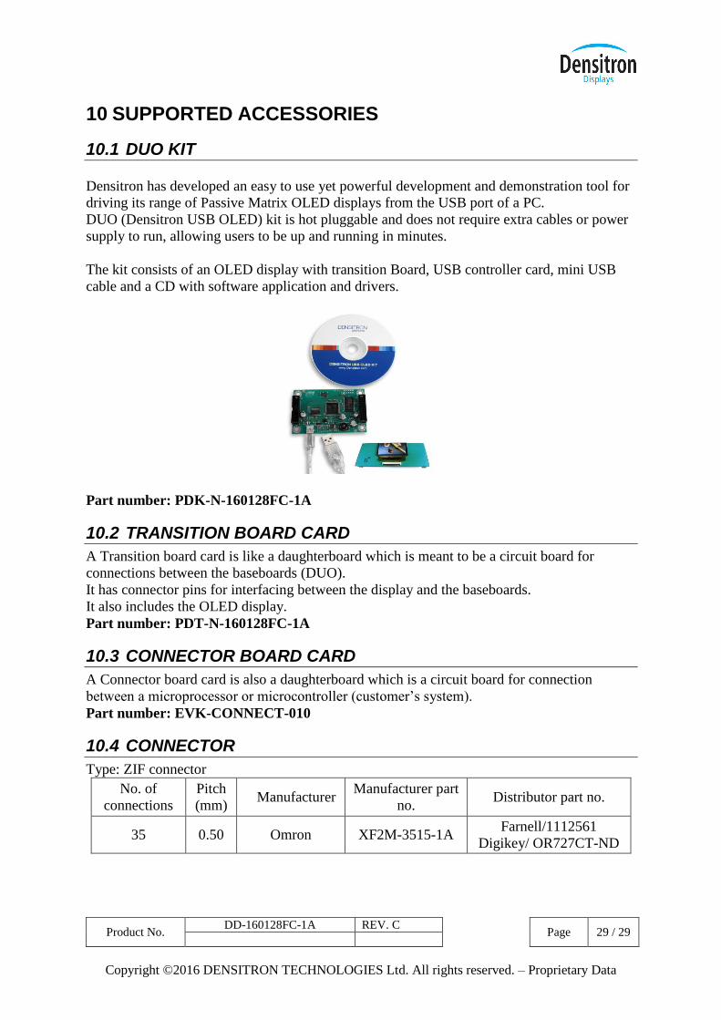
10.1 DUO KIT
Densitron has developed an easy to use yet powerful development and demonstration tool for
driving its range of Passive Matrix OLED displays from the USB port of a PC.
DUO (Densitron USB OLED) kit is hot pluggable and does not require extra cables or power
supply to run, allowing users to be up and running in minutes.
The kit consists of an OLED display with transition Board, USB controller card, mini USB
cable and a CD with software application and drivers.
Part number: PDK-N-160128FC-1A
10.2 TRANSITION BOARD CARD
A Transition board card is like a daughterboard which is meant to be a circuit board for
connections between the baseboards (DUO).
It has connector pins for interfacing between the display and the baseboards.
It also includes the OLED display.
Part number: PDT-N-160128FC-1A
10.3 CONNECTOR BOARD CARD
A Connector board card is also a daughterboard which is a circuit board for connection
between a microprocessor or microcontroller (customer’s system).
Part number: EVK-CONNECT-010
10.4 CONNECTOR
Type: ZIF connector
No. of
connections
Pitch
(mm) Manufacturer
Manufacturer part
no. Distributor part no.
35 0.50 Omron XF2M-3515-1A Farnell/1112561
Digikey/ OR727CT-ND