Embed Size (px)
Citation preview

CMOS Sensor, Inc. Slide-1
Proprietary & confidential24005 Stevens Creek Blvd., #1A, Cupertino, CA 95014
Tel: +1-408-366-2898 Fax: +1-408-366-2841
Jan. 5 & 6, 2011

CMOS Sensor, Inc. Slide-2
Proprietary & confidential24005 Stevens Creek Blvd., #1A, Cupertino, CA 95014
Tel: +1-408-366-2898 Fax: +1-408-366-2841
Outline
• Image sensor technology History
• Problems of conventional CMOS APS technology
• Technology for space sensor
• Space sensor
– C640 - 3D Terrain Mapping Camera (TMC)
– C650 - Hyper Spectral Imager (HySI)
– Radiation testing for C640 and C650
– C468 - PAN and MS Remote Sensing Instrument (RSI)

CMOS Sensor, Inc. Slide-3
Proprietary & confidential24005 Stevens Creek Blvd., #1A, Cupertino, CA 95014
Tel: +1-408-366-2898 Fax: +1-408-366-2841
Image sensor technology (1)
1968 [1T, Passive Pixel Sensor (PPS)] Gene Weckler
first solid state image sensor--> Charge readout
1969 (CCD) Boyle & Smith @ Bell Lab
first CCD image sensor
Sensing area
X shift register
Q = (IL + ID) * Tint
Blooming problem
Charge
integrator
Vout = [(QL+QD) / (Cd + Cp)] * G
CCD
Vout
rg
VDD
Vout = [(QL+QD+ Qp) / Co] * G
Y sh
ift registe
r
Self scan photo diode array

CMOS Sensor, Inc. Slide-4
Proprietary & confidential24005 Stevens Creek Blvd., #1A, Cupertino, CA 95014
Tel: +1-408-366-2898 Fax: +1-408-366-2841
Image sensor technology (2)
1988 (2T, PPS MOS) Bill Wang @ EG&G Reticon
First CMOS image sensor
1984 ~ 1990 Jim Janesick at JPL
First Scientific CCD (Hubble telescope)
Operation: MPP, OPP
Process: Flash oxide, flash gate,
backside illumination
Testing: Photo transfer curve
Sw
eep o
ut reg
ister
Read
out reg
ister
X register
Build in anti-blooming structure:
Blooming free

CMOS Sensor, Inc. Slide-5
Proprietary & confidential24005 Stevens Creek Blvd., #1A, Cupertino, CA 95014
Tel: +1-408-366-2898 Fax: +1-408-366-2841
Image sensor technology (3)
• 2003 (4T, APS CMOS)
PIN photodiode
High sensitivity
Electronic shutter
Blue response
Low dark leakage
V = [(QL + QD) / Co] * G
• 1992 [3T, Active Pixel Sensor (APS)] Eric
Fossom @ JPL
First CMOS APS image sensor
SF
mux
V = [(QL + QD ) / (Cd + Co)] * G
= [(IL + ID)* Tint / (Cd + Co)] * G

CMOS Sensor, Inc. Slide-6
Proprietary & confidential24005 Stevens Creek Blvd., #1A, Cupertino, CA 95014
Tel: +1-408-366-2898 Fax: +1-408-366-2841
APS CMOS Sensor
Pixel & CDS Block diagramsha
shd
QL + QD
SFVdout
Vaout
CDS circuitry
Vout = Vaout – Vdout ~ QL
Sensing area
pixelY
de
co
de
r
X decoder
CDS circuitry
Block diagram of the standard
APS image sensor
Y d
ecoder

CMOS Sensor, Inc. Slide-7
Proprietary & confidential24005 Stevens Creek Blvd., #1A, Cupertino, CA 95014
Tel: +1-408-366-2898 Fax: +1-408-366-2841
Problems of the conventional APS (1)
for high performance, high resolution device
1. Process variation:
Channel length variation (L 10%)
across whole wafer
gain and offset variation
L FF
pixel size
Loading parasitic capacitor
Speed
Pixel portion (source follower)
CDS portion (source follower)
2. Power and ground noise
10uA
Vdd
# 1 # 2 # 1303
# 1304

CMOS Sensor, Inc. Slide-8
Proprietary & confidential24005 Stevens Creek Blvd., #1A, Cupertino, CA 95014
Tel: +1-408-366-2898 Fax: +1-408-366-2841
Problems of the conventional APS (2)
for high performance, high resolution device
Cause
Fixed Pattern Noise
(FPN) problem
# 1
# 2
# 976

CMOS Sensor, Inc. Slide-9
Proprietary & confidential24005 Stevens Creek Blvd., #1A, Cupertino, CA 95014
Tel: +1-408-366-2898 Fax: +1-408-366-2841
Our Technology (1), patent pending
• Advanced APS pixel instead of APS readout structure on the sensor array to eliminate the fixed pattern noise (FPN) due to wafer process variation, power line voltage drop and signal line voltage drop problem.
• Buffer Mux instead of source follower readout structure on the CDS circuitry to eliminate the fixed pattern noise (FPN) due to wafer process variation.

CMOS Sensor, Inc. Slide-10
Proprietary & confidential24005 Stevens Creek Blvd., #1A, Cupertino, CA 95014
Tel: +1-408-366-2898 Fax: +1-408-366-2841
Performance comparisons (1)
With gain x 20
50 mV signal on each pixel
1 V output
Standard APS circuitry and source follower:
Standard wafer process:
Dark signal non-uniformity (FPN) ~ 1 V
Fine tune wafer process with small channel length variation
Dark signal non-uniformity (FPN) ~ 200 mV
5 times improved
CMOS Sensor’s new technology
Standard wafer process
Dark signal non-uniformity (FPN) < 20 mV
More than 50 times improved

CMOS Sensor, Inc. Slide-11
Proprietary & confidential24005 Stevens Creek Blvd., #1A, Cupertino, CA 95014
Tel: +1-408-366-2898 Fax: +1-408-366-2841
Space sensor
• C640 for 3D Terrain mapping camera (TMC)
• Moon orbit – 100 km
• 20 km swath
• 5 meter resolution
• C650 for Hyper-spectral imager camera (HySI)
• Moon orbit – 100 km
• 20 km swath
• 80 meter spatial resolution
• 452 nm ~ 964 nm spectral range
• 1 nm spectral resolution
• C468 for Remote Sensing Instrument (RSI)
• Earth orbit – 720 km
• 24 km swath
• 2 meter resolution (PAN)
• 4 meter resolution (MS)
• 4 MS band (R, G, B, and NIR)
• 5 CMOS TDI
• 120 mm CMOS Image Sensor
C650 C640
C468

CMOS Sensor, Inc. Slide-12
Proprietary & confidential24005 Stevens Creek Blvd., #1A, Cupertino, CA 95014
Tel: +1-408-366-2898 Fax: +1-408-366-2841
C640 (TMC)
• 4000 linear image sensor, PGA, 12 bit ADC output
• Destructive / Non destructive readout mode
• Global exposure control pin to control integration time
• Low fixed pattern noise
• Very high dynamic range
First Space Qualified Digital Image Sensor
Enters
Moon Orbit

CMOS Sensor, Inc. Slide-13
Proprietary & confidential24005 Stevens Creek Blvd., #1A, Cupertino, CA 95014
Tel: +1-408-366-2898 Fax: +1-408-366-2841
Moon mission
Japan China India USASatellite Kaguya Chang’e-1 Chandrayaan-1 Lunar
Reconnaissance
Orbiter
Overall Weight 3.0 tons 2.3 tons 1.4 tons
Launch Date September 2007 October 2007 October 2008 June 2009
Camera Type Terrain Camera &
Multi Band
3D Terrain
Mapping
3D Terrain
Mapping
3D Terrain Mapping
Sensor CCD CCD CMOS (C640) CCD
Weight 9.4 kg > 30 kg 6.3 kg 9.8 kg
Power > 10 watts 1.8 watts 20 watts
RadiationCCD CMOS
< 100 krad > 300 krad

CMOS Sensor, Inc. Slide-14
Proprietary & confidential24005 Stevens Creek Blvd., #1A, Cupertino, CA 95014
Tel: +1-408-366-2898 Fax: +1-408-366-2841
Terrain Mapping Camera
Direction of Travel
Aft Nadir Fore
20 km => 5m
500 nm – 750 nm
3 CMOS Sensors
Fore Nadir & Aft
Push Broom Mode
Stereo View
+/- 25 degrees

CMOS Sensor, Inc. Slide-15
Proprietary & confidential24005 Stevens Creek Blvd., #1A, Cupertino, CA 95014
Tel: +1-408-366-2898 Fax: +1-408-366-2841
Evaluation board (FPA)
Linear sensor
23 cm (L) x 8.5 cm (W) x 1.5 cm (H)

CMOS Sensor, Inc. Slide-16
Proprietary & confidential24005 Stevens Creek Blvd., #1A, Cupertino, CA 95014
Tel: +1-408-366-2898 Fax: +1-408-366-2841
Sensor Block Diagram
Green – Digital Red – Analog Blue – Mixed Mode
4000 element array, 7 um x 7 um pixel size, Fixed Pattern Suppression,
Anti Blooming Control, Dark Voltage Cancellation, Global Exposure
Control, Timing Generator, Power Down Mode, LVDS TX & RX, Band
Gap & Voltage Regulators

CMOS Sensor, Inc. Slide-17
Proprietary & confidential24005 Stevens Creek Blvd., #1A, Cupertino, CA 95014
Tel: +1-408-366-2898 Fax: +1-408-366-2841
Device Feature
• Single video readout, 12 bit resolution, serial readout mode
• Three operational modes:
– Destructive readout mode
– Non destructive readout mode, up to 32 frame
– Power Down mode
• Snap Shot Operation • Global exposure control function (no integration will take place till exposure
control is active) • Electronic Shutter is controlled by Exposure Pulse (EP)
• Auto dark voltage cancellation and fixed pattern noise cancellation
• Programmable gain control feature:
– Two bits for Coarse gain of (x1, x2, x3, and x4)
– Three bits for Fine gain of 10%
• ADC input selects either internal PGA output or external input voltage
• Clock input and data output are LVDS interface

CMOS Sensor, Inc. Slide-18
Proprietary & confidential24005 Stevens Creek Blvd., #1A, Cupertino, CA 95014
Tel: +1-408-366-2898 Fax: +1-408-366-2841
Operation: Destructive
• SP
• EP
• Reset
• Transfer
• Photodiode
• Vout
F1 F2 F3 F4
F1 F2 F3
S1
S2
STr
SReset

CMOS Sensor, Inc. Slide-19
Proprietary & confidential24005 Stevens Creek Blvd., #1A, Cupertino, CA 95014
Tel: +1-408-366-2898 Fax: +1-408-366-2841
Operation: Non-Destructive
• SP
• EP
• Reset
• Transfer
• Photodiode
• Vout
S1
S2
STr
SReset
F1 F2 F3 F4
F1 F2 F3
F1 F2 F3 F4
F1 F2 F3

CMOS Sensor, Inc. Slide-20
Proprietary & confidential24005 Stevens Creek Blvd., #1A, Cupertino, CA 95014
Tel: +1-408-366-2898 Fax: +1-408-366-2841
Dynamic Range
Measured Dynamic Range:
DR = 20 x Log (21653 / 0.015) = 123.2 dB
Operating Mode Illumination
(Candela/m2)
Output
(DN)
Sensor Noise
(DN)
SNR
Destructive Read 21653 4010 6.78 591.4
Non Destructive Read 0.015 15.7 15.2 1

CMOS Sensor, Inc. Slide-21
Proprietary & confidential24005 Stevens Creek Blvd., #1A, Cupertino, CA 95014
Tel: +1-408-366-2898 Fax: +1-408-366-2841
Dark signal non-uniformity
Dark signal
0
20
40
60
1 282 563 844 1125 1406 1687 1968 2249 2530 2811 3092 3373 3654 3935
pixel number
Am
pli
tude (
DN
)

CMOS Sensor, Inc. Slide-22
Proprietary & confidential24005 Stevens Creek Blvd., #1A, Cupertino, CA 95014
Tel: +1-408-366-2898 Fax: +1-408-366-2841
Light signal

CMOS Sensor, Inc. Slide-23
Proprietary & confidential24005 Stevens Creek Blvd., #1A, Cupertino, CA 95014
Tel: +1-408-366-2898 Fax: +1-408-366-2841
Photon transfer curve
Noise floor
Saturation
charge
Conversion rate
Shot noise

CMOS Sensor, Inc. Slide-24
Proprietary & confidential24005 Stevens Creek Blvd., #1A, Cupertino, CA 95014
Tel: +1-408-366-2898 Fax: +1-408-366-2841
MTF & Non-linearity
Non-Linearity
< 0.1% between 10% and 90% Well Capacity
Measured by Ramping Illumination
Wavelength MTF @ Nyquist spatial frequency
Blue light source 470 nm 78%
Green light source 560 nm 68%
Red light source 640 nm 50%
Near Infrared light 940 nm 25%
White light (CCFL) 70%
MTF

CMOS Sensor, Inc. Slide-25
Proprietary & confidential24005 Stevens Creek Blvd., #1A, Cupertino, CA 95014
Tel: +1-408-366-2898 Fax: +1-408-366-2841
Earth image from TMC (70,000 km)

CMOS Sensor, Inc. Slide-26
Proprietary & confidential24005 Stevens Creek Blvd., #1A, Cupertino, CA 95014
Tel: +1-408-366-2898 Fax: +1-408-366-2841
Moon image from TMC (311,200 km)

CMOS Sensor, Inc. Slide-27
Proprietary & confidential24005 Stevens Creek Blvd., #1A, Cupertino, CA 95014
Tel: +1-408-366-2898 Fax: +1-408-366-2841
Moon image from TMC (100 km)

CMOS Sensor, Inc. Slide-28
Proprietary & confidential24005 Stevens Creek Blvd., #1A, Cupertino, CA 95014
Tel: +1-408-366-2898 Fax: +1-408-366-2841
3D Moon image from TMC

CMOS Sensor, Inc. Slide-29
Proprietary & confidential24005 Stevens Creek Blvd., #1A, Cupertino, CA 95014
Tel: +1-408-366-2898 Fax: +1-408-366-2841
3D Moon image from TMC

CMOS Sensor, Inc. Slide-30
Proprietary & confidential24005 Stevens Creek Blvd., #1A, Cupertino, CA 95014
Tel: +1-408-366-2898 Fax: +1-408-366-2841
3D Moon image from TMC

CMOS Sensor, Inc. Slide-31
Proprietary & confidential24005 Stevens Creek Blvd., #1A, Cupertino, CA 95014
Tel: +1-408-366-2898 Fax: +1-408-366-2841
3D Moon image from TMC

CMOS Sensor, Inc. Slide-32
Proprietary & confidential24005 Stevens Creek Blvd., #1A, Cupertino, CA 95014
Tel: +1-408-366-2898 Fax: +1-408-366-2841
3D Moon image from TMC

CMOS Sensor, Inc. Slide-33
Proprietary & confidential24005 Stevens Creek Blvd., #1A, Cupertino, CA 95014
Tel: +1-408-366-2898 Fax: +1-408-366-2841

CMOS Sensor, Inc. Slide-34
Proprietary & confidential24005 Stevens Creek Blvd., #1A, Cupertino, CA 95014
Tel: +1-408-366-2898 Fax: +1-408-366-2841

CMOS Sensor, Inc. Slide-35
Proprietary & confidential24005 Stevens Creek Blvd., #1A, Cupertino, CA 95014
Tel: +1-408-366-2898 Fax: +1-408-366-2841

CMOS Sensor, Inc. Slide-36
Proprietary & confidential24005 Stevens Creek Blvd., #1A, Cupertino, CA 95014
Tel: +1-408-366-2898 Fax: +1-408-366-2841

CMOS Sensor, Inc. Slide-37
Proprietary & confidential24005 Stevens Creek Blvd., #1A, Cupertino, CA 95014
Tel: +1-408-366-2898 Fax: +1-408-366-2841

CMOS Sensor, Inc. Slide-38
Proprietary & confidential24005 Stevens Creek Blvd., #1A, Cupertino, CA 95014
Tel: +1-408-366-2898 Fax: +1-408-366-2841
C650 (HySI)
• 256 x 512 area sensor, PGA, 12 bit ADC output
• 50 um x 50 um pixel size
• Snap shot function, up to 250 ms integration time
• Row wise response compensation,
• dark voltage cancellation
• < 1 % of the linearity
A novel digital image sensor with row wise gain
compensation for
Hyper Spectral Imager (HySI) application

CMOS Sensor, Inc. Slide-39
Proprietary & confidential24005 Stevens Creek Blvd., #1A, Cupertino, CA 95014
Tel: +1-408-366-2898 Fax: +1-408-366-2841
HySI Imaging Camera
Camera: focusing optics, wedge filter, CMOS image sensor, camera electronics &
housing. Wedge filter for simplicity & compactness.
Focusing optics: 5 element, telecentric, refracting lens w circular fov of +/- 13 deg.
Result: Weight: 2.5 kg; Power: 1.0 watt
Goal: Light Weight; Low Power

CMOS Sensor, Inc. Slide-40
Proprietary & confidential24005 Stevens Creek Blvd., #1A, Cupertino, CA 95014
Tel: +1-408-366-2898 Fax: +1-408-366-2841
HySI Imaging Camera
256 x 512 element CMOS Image Sensor Array
Push Broom Mode (100 km)
20 km cross track view
Spatial Resolution: 80 m
Spectral Range: 421 nm – 964 nm
Spectral Resolution: <1 nm
36 MHz => 20 Frames/sec

CMOS Sensor, Inc. Slide-41
Proprietary & confidential24005 Stevens Creek Blvd., #1A, Cupertino, CA 95014
Tel: +1-408-366-2898 Fax: +1-408-366-2841
Sensor Block Diagram
Green – Digital Red – Analog Blue – Mixed Mode
Column Readout
256 x 512
Photodiode Array
Pre
S/H
DVC
PGAADC L
VD
S T
X
Format
Regulator
Latch
LVDS RX
Timing Generator
I2C & SRAM
OP
CLK EP SP
Se
rial
Pa
ralle
lHGEN_DVCV_SELD_SEL
256 x 512 array, Fixed Pattern Suppression,
Anti Blooming Control, Dark Voltage
Cancellation, Global Exposure Control,
Timing Generator, Power Down Mode, LVDS
TX & RX, Band Gap & Voltage Regulators

CMOS Sensor, Inc. Slide-42
Proprietary & confidential24005 Stevens Creek Blvd., #1A, Cupertino, CA 95014
Tel: +1-408-366-2898 Fax: +1-408-366-2841
Device Feature
• 50 um x 50 um pixel size
• 50 um element pitch on both horizontal and vertical direction
• 256 x 512 active elements
• 25.6 mm x 12.8 mm image size
• Single video out, 12 bit resolution, serial or parallel readout mode
• Three operating modes:
normal image capture mode,
row wise gain readout mode
power down
• Snap Shot operation
• Global exposure control function. No integration till EP on
• Coarse gain of (x1 and x2)
• Row wise gain setting: seven bits for gain equals to 1 to 5
• I2C & SRAM interface feature:
• ADC input selection either internal PGA or external input voltage
• The gain setting is latched by an external latch start pulse (LSP)

CMOS Sensor, Inc. Slide-43
Proprietary & confidential24005 Stevens Creek Blvd., #1A, Cupertino, CA 95014
Tel: +1-408-366-2898 Fax: +1-408-366-2841
Operation: PGA Block
Column Readout
256 x 512
Photodiode Array
Pre
S/H
DVC
PGAADC L
VD
S T
X
Format
Normalize Signal in
S/W or H/W.
I2C Interface
7-bit gain level
1x to 5x
Non-Linearity <0.1%
Patent pending

CMOS Sensor, Inc. Slide-44
Proprietary & confidential24005 Stevens Creek Blvd., #1A, Cupertino, CA 95014
Tel: +1-408-366-2898 Fax: +1-408-366-2841
Measured SNR
Measured SNR
Full Well Cap.
90 % Well Cap. 501 - 512
50 % Well Cap. 243 - 255
1 % Well Cap. 4 - 6

CMOS Sensor, Inc. Slide-45
Proprietary & confidential24005 Stevens Creek Blvd., #1A, Cupertino, CA 95014
Tel: +1-408-366-2898 Fax: +1-408-366-2841
MTF & Non-linearity
Non-Linearity
< 0.5% for 10% to 90% Well Capacity (any pixel)
Measured by Ramping Illumination
Wavelength MTF value @ Nyquist spatial frequency
Blue light source 470 nm 99%
Green light source 560 nm 99%
Red light source 640 nm 99%
Near Infrared light 940 nm 98%
White light (CCFL) 99%
Along track MTF (512 row direction)
Wavelength MTF value @ Nyquist spatial frequency
Blue light source 470 nm 96%
Green light source 560 nm 96%
Red light source 640 nm 95%
Near Infrared light 940 nm 92%
White light (CCFL) 95%
Across track MTF (256 column direction)

CMOS Sensor, Inc. Slide-46
Proprietary & confidential24005 Stevens Creek Blvd., #1A, Cupertino, CA 95014
Tel: +1-408-366-2898 Fax: +1-408-366-2841
Image Performance
Equatorial Region Crater let Barrow H
Subtle colorations are enhanced by rationing and/or subtracting bands.

CMOS Sensor, Inc. Slide-47
Proprietary & confidential24005 Stevens Creek Blvd., #1A, Cupertino, CA 95014
Tel: +1-408-366-2898 Fax: +1-408-366-2841
Image Performance
Hypercube
64 Spectral Bands Stacked
Unique Spectral Signature @ Each Location

CMOS Sensor, Inc. Slide-48
Proprietary & confidential24005 Stevens Creek Blvd., #1A, Cupertino, CA 95014
Tel: +1-408-366-2898 Fax: +1-408-366-2841
Summary
A Hyper-Spectral camera utilizing CMOS image sensor technology , was used to scan the lunar surface, generating mineralogical maps unmatched by any prior survey.
The camera’s light weight and low power could only be achieved using CMOS image sensor technology and design techniques.

CMOS Sensor, Inc. Slide-49
Proprietary & confidential24005 Stevens Creek Blvd., #1A, Cupertino, CA 95014
Tel: +1-408-366-2898 Fax: +1-408-366-2841
Radiation testing
of
Chandrayaan-1 space sensor

CMOS Sensor, Inc. Slide-50
Proprietary & confidential24005 Stevens Creek Blvd., #1A, Cupertino, CA 95014
Tel: +1-408-366-2898 Fax: +1-408-366-2841
Radiation chamber testing setup The detector card with CMOS imaging sensor is placed in the Gamma ray irradiation
chamber which is self shielded Cobalt-60 Gamma irradiator. Fig shows the irradiation
chamber is located in vertical shaft inside a lead shield. The shaft moves up and down with
the help of motorized drive which enables the placement of detector in irradiation chamber
as shown in Fig. Accesses holes are provided in the vertical shaft through which bias lines are
provided to the CMOS sensor for active radiation testing.
7.5 rad / sec

CMOS Sensor, Inc. Slide-51
Proprietary & confidential24005 Stevens Creek Blvd., #1A, Cupertino, CA 95014
Tel: +1-408-366-2898 Fax: +1-408-366-2841
E-O testing setup
DUT: linear sensor and area sensor

CMOS Sensor, Inc. Slide-52
Proprietary & confidential24005 Stevens Creek Blvd., #1A, Cupertino, CA 95014
Tel: +1-408-366-2898 Fax: +1-408-366-2841
Testing data (1)
Fig 5: Dark Offset and Dark current variation with Radiation dose for linear
array and area array CMOS sensor

CMOS Sensor, Inc. Slide-53
Proprietary & confidential24005 Stevens Creek Blvd., #1A, Cupertino, CA 95014
Tel: +1-408-366-2898 Fax: +1-408-366-2841
Testing data (2)
Fig 6: Noise floor variation as a function of radiation dose
at nominal and ten times increased integration time for area
array

CMOS Sensor, Inc. Slide-54
Proprietary & confidential24005 Stevens Creek Blvd., #1A, Cupertino, CA 95014
Tel: +1-408-366-2898 Fax: +1-408-366-2841
Testing data (3)
Fig 7: Fixed pattern Noise measurement as a function of
radiation dose for linear array and Area array CMOS sensor.

CMOS Sensor, Inc. Slide-55
Proprietary & confidential24005 Stevens Creek Blvd., #1A, Cupertino, CA 95014
Tel: +1-408-366-2898 Fax: +1-408-366-2841
Testing data (5)
After
Annealing
Fig 10: Dark signal
reduction with annealing
Fig : FPN reduction
with annealing

CMOS Sensor, Inc. Slide-56
Proprietary & confidential24005 Stevens Creek Blvd., #1A, Cupertino, CA 95014
Tel: +1-408-366-2898 Fax: +1-408-366-2841
Testing summary
• Both linear and area CMOS active pixel sensor was
subjected to total ionization dose radiation testing
up to 300 Krad, there was no catastrophic failure
encountered during the test.
• The different detector parameters and there effect
was studied in detail and this experiment gives a
vision on the future designs of CMOS image sensor
for space mission.

CMOS Sensor, Inc. Slide-57
Proprietary & confidential24005 Stevens Creek Blvd., #1A, Cupertino, CA 95014
Tel: +1-408-366-2898 Fax: +1-408-366-2841
C468 (RSI) sensor
• PAN: 12,000 pixels, 10 um x 10 um pixel size
• MS: 6,000 pixels, 20 um x 20 um pixel size
• MS: 4 bands (B, G, R, NIR)
• Line rate: PAN: 0.3 ms / line; MS: 0.6 ms / line
• Image length: 120 mm
• No band to band registration error
• No pixel to pixel or band to band peak to peak elevation variation
• No any missing pixel along image length

CMOS Sensor, Inc. Slide-58
Proprietary & confidential24005 Stevens Creek Blvd., #1A, Cupertino, CA 95014
Tel: +1-408-366-2898 Fax: +1-408-366-2841
Long sensor chip requirement
Chip size
pixel size: 10 um (20 um)
Pixel number: 12,000 (6,000) pixels
Image length: 120 mm
Not missing pixel or registration error is required

CMOS Sensor, Inc. Slide-59
Proprietary & confidential24005 Stevens Creek Blvd., #1A, Cupertino, CA 95014
Tel: +1-408-366-2898 Fax: +1-408-366-2841
Chip size overview (1)
CCD technology using 1 x stepper or proximity alignment, > 1 um technology
Field size: = wafer size
Advantage: Large chip is possible
Drawback: Old semiconductor technology
CMOS technology using 5 x scanner or 5 x stepper, < 1 um technology
Field size: ~ 35 mm x 25 mm (scanner)
~ 24 mm x 22 mm (stepper)
Advantage: Advanced technology
Drawback: Chip size is limited by the field size.
Long chip size is impossible

CMOS Sensor, Inc. Slide-60
Proprietary & confidential24005 Stevens Creek Blvd., #1A, Cupertino, CA 95014
Tel: +1-408-366-2898 Fax: +1-408-366-2841
Chip size overview (2)Methods to achieve long sensor size:
1. Wafer Stitching technology: using several masks process on
same wafer
Advantage: Chip performance is good
Drawback: Several mask set per chip, thru put is low. Very high cost
2. Silicon butting technology: Butting silicon chip on substrate
Advantage: Long sensor length (up to 3 meter long), cheaper
Drawback: Gap between two chips (~ 10 um), tolerance, registration error.
Substrate Sensor chip
10 ~ 20 um
This technology is very useful on chip design and mask design. They are
different from standard IC technology.
Chip design: No sealing ring, layout, edge pixel design, uniformity, …
Mask design: No PCM and alignment key on the scribe line

CMOS Sensor, Inc. Slide-61
Proprietary & confidential24005 Stevens Creek Blvd., #1A, Cupertino, CA 95014
Tel: +1-408-366-2898 Fax: +1-408-366-2841
Chip size overview (3)
3. Wafer butting technology (require high wafer yield, patent pending)
Combine the advantage of wafer stitching technology and silicon butting technology
No scribe line on the sensing area; Move scribe line inside the sensor chip; select several good chips to form a long sensor array.
Advantage: Good performance, low cost, Long sensor chip is possible (12000, 16000, 20000,..)
Drawback: Difficult for chip design and layout.
3000 pixels 3000 pixels 3000 pixels
~ 30 mm ~ 30 mm ~ 30 mm
3000 pixels
~ 30 mm
Photo detector arrayScribe line
CMOS Sensor, Inc. Slide-62
Proprietary & confidential24005 Stevens Creek Blvd., #1A, Cupertino, CA 95014
Tel: +1-408-366-2898 Fax: +1-408-366-2841
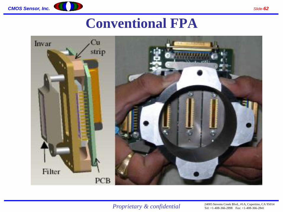
Conventional FPA

CMOS Sensor, Inc. Slide-63
Proprietary & confidential24005 Stevens Creek Blvd., #1A, Cupertino, CA 95014
Tel: +1-408-366-2898 Fax: +1-408-366-2841
Sensor on focal plane (conventional method)
12.7
6
12.7
6
12.7
6
12.7
6
12.7
87.5
120
74.8
Optical focal plane
141
CCD
Ceramic
package
(unit mm)

CMOS Sensor, Inc. Slide-64
Proprietary & confidential24005 Stevens Creek Blvd., #1A, Cupertino, CA 95014
Tel: +1-408-366-2898 Fax: +1-408-366-2841
Problem of the conventional method
• Band to band registration
error (R, G, B, NIR)
• Band to band parallelism
• Pixel to pixel flatness
• Large Optical focal plane
> 10 mm
> 10 mm
10 ~ 20 um
Registration error

CMOS Sensor, Inc. Slide-65
Proprietary & confidential24005 Stevens Creek Blvd., #1A, Cupertino, CA 95014
Tel: +1-408-366-2898 Fax: +1-408-366-2841
Our design approach
• Using microelectronic technology to integrate 5
rows of the sensor into a tiny silicon chip and
assemble on a single ceramic package
– CMOS Sensor instead of CCD
– Integrate ADC with sensor (digital and analog circuitry)
– Wafer butting technology to achieve 120 mm long
– Multiple chip technology to combine 5 bands into one
silicon chip
– Multiple output structure to achieve high frame rate
– CMOS TDI (Time Delay Integration) technology to
achieve high SNR
Patent pending

CMOS Sensor, Inc. Slide-66
Proprietary & confidential24005 Stevens Creek Blvd., #1A, Cupertino, CA 95014
Tel: +1-408-366-2898 Fax: +1-408-366-2841
Difficult area and our approach
• Long sensor chip requirement:
– Wafer butting technology (patent pending)
• Multiple System on Chip (MSOC) requirement:
– Wafer scale assembly technology (patent pending)
• S/N requirement:
– CMOS TDI (Time Delay Integration) structure (patent pending)

CMOS Sensor, Inc. Slide-67
Proprietary & confidential24005 Stevens Creek Blvd., #1A, Cupertino, CA 95014
Tel: +1-408-366-2898 Fax: +1-408-366-2841
Whole array
30 mm
25 mm
120 mm
<1> <2> <3> <4>
One chip size: 30 mm x 25 mm
Four chip size: 120 mm x 25 mm
30 mm 30 mm 30 mm

CMOS Sensor, Inc. Slide-68
Proprietary & confidential24005 Stevens Creek Blvd., #1A, Cupertino, CA 95014
Tel: +1-408-366-2898 Fax: +1-408-366-2841
MS 4 chips light signal (room light)
B3
B4

CMOS Sensor, Inc. Slide-69
Proprietary & confidential24005 Stevens Creek Blvd., #1A, Cupertino, CA 95014
Tel: +1-408-366-2898 Fax: +1-408-366-2841
MS 4 chips dark signal
B3
B4

CMOS Sensor, Inc. Slide-70
Proprietary & confidential24005 Stevens Creek Blvd., #1A, Cupertino, CA 95014
Tel: +1-408-366-2898 Fax: +1-408-366-2841
MS 4 chips dark noise floor
B3
B4

CMOS Sensor, Inc. Slide-71
Proprietary & confidential24005 Stevens Creek Blvd., #1A, Cupertino, CA 95014
Tel: +1-408-366-2898 Fax: +1-408-366-2841
Sensor & package
130 pin PGA, Pin on two side
155 mm x 60 mm size

CMOS Sensor, Inc. Slide-72
Proprietary & confidential24005 Stevens Creek Blvd., #1A, Cupertino, CA 95014
Tel: +1-408-366-2898 Fax: +1-408-366-2841
FPA (Microelectronic method)
4 4
2460
chip
Ceramic
package
Optical focal plane
~ 121 mm
Unit: mm
120
155

CMOS Sensor, Inc. Slide-73
Proprietary & confidential24005 Stevens Creek Blvd., #1A, Cupertino, CA 95014
Tel: +1-408-366-2898 Fax: +1-408-366-2841
FPA (Micro electronic method)
4 2 5
2030
chip
Ceramic
package
30
6
Optical focal plane
< 131 mm
Unit: mm
120
150
66
20

CMOS Sensor, Inc. Slide-74
Proprietary & confidential24005 Stevens Creek Blvd., #1A, Cupertino, CA 95014
Tel: +1-408-366-2898 Fax: +1-408-366-2841
Thank you