Embed Size (px)
Citation preview
Transworld Research Network 37/661 (2), Fort P.O., Trivandrum-695 023, Kerala, India
Electromagnetic, Magnetostatic, and Exchange-Interaction Vortices in Confined Magnetic Structures, 2008: 427-457 ISBN: 978-81-7895-373-1 Editor: E.O. Kamenetskii
20 Vortices in magnetic nano-rings
J. Sautner, N. Jahedi and V. Metlushko Nanotechnology Core Facility, University of Illinois at Chicago
Abstract Recent studies on Co, Ni and permalloy rings
have shown that a totally flux-closed magnetic vortex structure is stable at remanence. The two chiralities of the vortex, clockwise and counter-clockwise, have been proposed as the carriers for the stored information that could be read in a magneto-resistance-based device. It was found that magneto-optical imaging, Lorentz STEM (LSTEM) and scanning electron microscopy with polarization analysis (SEMPA) allow a direct determination of magnetic vortex chiralities and that bycontrolling the shape of the nanoscale magnetic ring and the direction of applied magnetic field we can precisely tune the switching mechanism and reliably predict the hi li f h
Correspondence/Reprint request: Dr. V. Metlushko, Nanotechnology Core Facility, University of Illinois at Chicago E-mail: [email protected]
J. Sautner 428
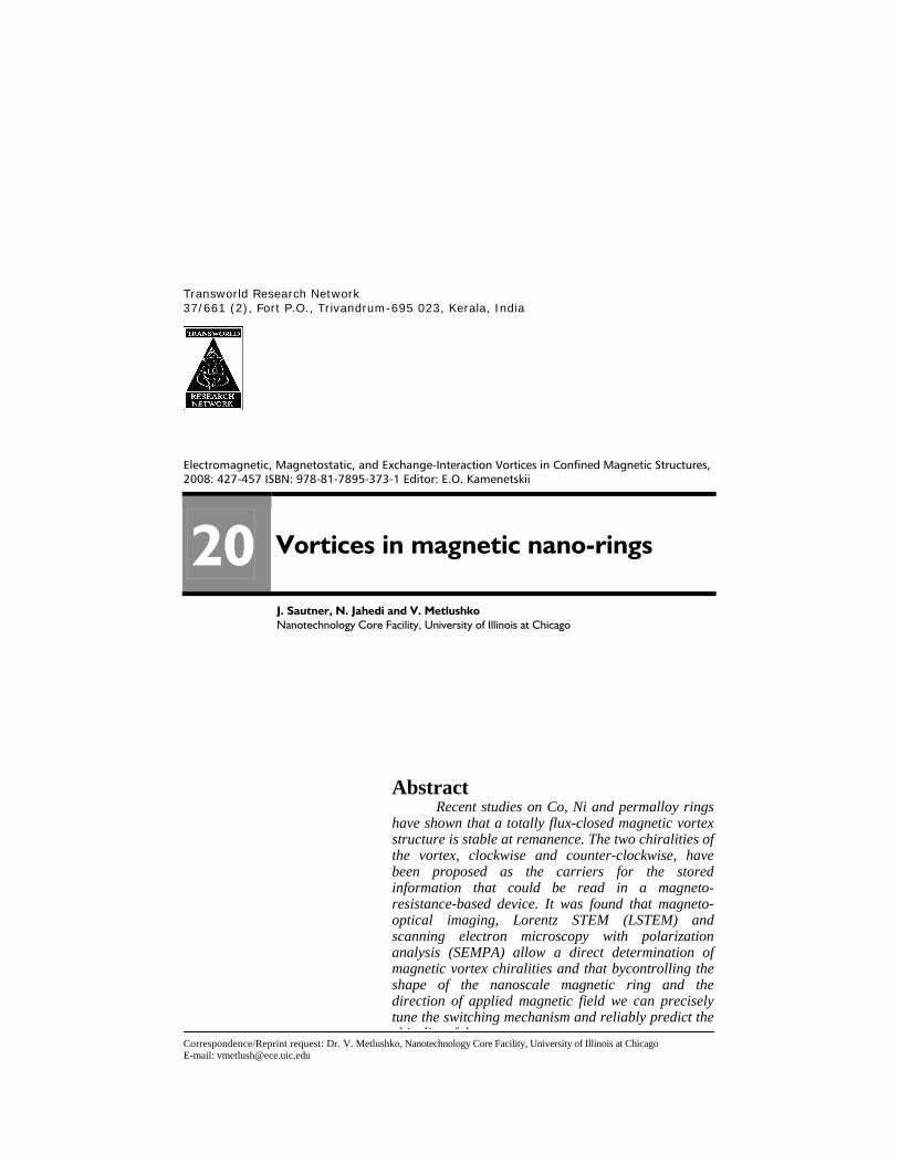
1. Introduction In the past few years, interest in magnetic nano-rings has increased rapidly because they offer potential applications in advanced memories and magnetic logic circuits [1-39]. For patterned magnetic materials, only in very few cases with well-defined anisotropies does the reversal take place via a coherent rotation of the magnetization. More common, however, is that the reversal occurs via the domain formation at the ends of the elongated element. For arbitrarily shaped nano-scale elements, in general, it has been impossible to reliably calculate the field at which the domain first forms from basic principles [40]. Recently, Zhu et al., proposed the use of circular ring element as the hard layer in vertical MRAM devices, with switching controlled by pulses of radial fields [41]. The rings exhibit two different stable “onion” states in addition to two “vortex”, or “flux” states. Two possible vortex states with clockwise or counter-clockwise rotation of the magnetic field (chirality) realized at remanence can be used for magnetic storage. Those states are magnetically stable since the highly energetic magnetic vortex core is removed, and they can be packed in high-density arrays because the flux-closed vortex state reduces interactions between neighboring elements [41]. 2. Switching process visualization Magnetic hysteresis loops of arrays of ring elements have been measured by SQUID magnetometry and the magneto-optical Kerr effect (MOKE). It must be noted that the hysteresis loops reflect the global sample magnetization, which is the result of an ensemble of magnetic states of the individual rings. It is assumed that each element behaved independently of its neighbors. However, modern fabrication techniques allow us to place the magnetic elements close enough together that element-element interactions compete with single-element energies, which can lead to totally different switching dynamics. To visualize the magnetization reversal process in individual rings as well as in high-density arrays, several different imaging techniques were employed - magnetic force microscopy (MFM) [22, 39] (Figs. 1 and 2), scanning Hall microscopy (SHM) [36] (Fig. 3), magneto-optical (MO) microscopy (Fig. 4) [19, 29], scanning electron microscopy with polarization analysis (SEMPA), and Lorentz microscopy (LM) (Fig. 5) [19].
(a) (b) (c) (d) Figure 1. Magnetization reversal process in the circular permalloy narrow ring: from onion (A) to vortex state (B) through domain wall propagation (A-B). (a) Scanning electron microscopy (SEM) image of a narrow permalloy ring; (b) MFM image of onion state (A) in the circular permalloy narrow ring; (c) MFM at H = 25 Oe; (d) MFM image of the vortex state (B), H=60 Oe [39].

Vortices in magnetic nano-rings 429
High spatial resolution and high sensitivity make MFM a very powerful tool for the study of the magnetic properties of ring elements [39]. Zhu et al., found that the narrow rings (Fig. 1a) exhibit two different, highly stable polarized (‘onion’) states (field lines split around the center in opposite directions with N and S poles meeting at opposite sides) in addition to the vortex states (field lines encircle the center) [39]. It was found experimentally that the reversal mechanism (Fig. 2a) for changing the magnetic state of the circular ring from the onion state to the vortex state occurs through domain wall propagation [4-6]. The typical time for magnetization reversal is expected to be a few nanoseconds or even less, substantially beyond the capability of many techniques such as MFM and MOKE. However, the propagating domain wall can be localized at various pinning sites (probably associated with sample defects), as shown in Fig. 1c. Fig. 1b shows the onion state at remanence; the wall starts to move at a field of about 25 Oe, and is pinned at another location as shown in Fig. 1c. The domain wall was de-pinned again at a larger field of 60 Oe, and completed the reversal process to a vortex state shown in Fig. 1d (where the contrast originated from the distorted vortex state in the presence of the external field). The propagation of the domain wall was found to be either clockwise or counterclockwise. Zhu et al. concluded that the reversal mechanism from the onion to the flux state is completed through a domain wall propagation process [39]. It was found that the switching field for the transition from the flux to the onion state is quite uniform. Defects, roughness, and size variations play a minor role in this switching process. This switching mode is very reproducible with a very narrow field distribution even for ensembles of rings. As a consequence, the flux state can be stabilized even for large ensembles in a very controllable manner within a wide field range. The reversal mechanism from the vortex to onion state is expected to be the same as the switching from one flux state to another by using circular magnetic fields [41]. Both occur through domain wall nucleation and thus demonstrate uniform switching fields. It is well known that the small stray field of MFM tips can change the magnetic state of the ring [39]. The MFM tips are usually coated with NiCo, NiFe, or CoPtCr and magnetized along their axis prior to imaging. To avoid problems with tip-ring interactions and to verify the validity of MFM data, test measurements on the ring arrays
A
B
C
D
(a) (b) (c) Figure 2. Magnetization reversal process in ring magnetic elements; (a) Schematic of the magnetization reversal process in ring magnetic element: two “onion” states (A) and (C) and two “vortex” states (B) and (D); (b) Magnetization loop of individual narrow permalloy ring determined by MFM. After [5]; (c) Magnetization loop of 100 permalloy rings determined by MFM. After [39].

J. Sautner 430
were performed by scanning Hall probe microscopy (SHPM) (Fig. 3). High-resolution SHPM is a recently-developed technique to image local magnetic fields. It is characterized by both high magnetic field sensitivity and high spatial resolution. The technique involves rastoring a micron-sized Hall probe just above the surface of the sample [36, 42, 43]. In a comparison between SHPM and MFM, SHPM’s major advantage is that it is a non-invasive technique, facilitating the visualization of magnetic structure in magnetic materials. The KUL/IMEC team just finished construction of an SHPM with high magnetic field sensitivity (~0.01 G) and high spatial resolution (~0.5 µm), operating in a He-cryostat. In their setup, a submicron Hall probe manufactured in a GaAs/AlGaAs or AlGaSb/InAs/(Al)GaSb two-dimensional electron gas is scanned over the sample to locally measure magnetic fields and image the magnetization reversal in micron rings (Fig. 3) [36]. There are several different high-resolution electron-microscopy techniques that were used for magnetic imaging. SEMPA has several unique capabilities that distinguish it from other magnetic imaging techniques: it provides a direct measurement of the magnetization chirality in the rings, and it has a high spatial resolution of about 10 nm. Lorentz microscopy is based on electron transmission through a thin magnetic film, and electron deflection due to the Lorentz force, which is proportional to the local magnetic field. It provides a very high resolution that is better than 10 nm, and also allows for the direct determination of the chirality of the magnetization of the ring. An obvious drawback of SEMPA and Lorentz microscopy is that only small or no external magnetic fields can be applied during the measurements. If not only remanent magnetization states, but also states in the presence of external magnetic fields (e.g. during the process of magnetization reversal) are to be studied, optical microscopy is preferable. Magneto-optical (MO) microscopy is a well-established microscopy technique. A magneto-optical microscope is basically a conventional polarization microscope where the specimen is illuminated with polarized light. The reflected light passes through an analyzer and is collected by the objective lens of the microscope. Ring samples examined by Welp, et al. are imaged in reflection mode, and magnetic contrast is obtained by detecting the magneto-optical Kerr effect (Kerr microscopy) [19]. MO imaging allows for not only
(a) (b) (c) (d) Figure 3. High-resolution SHPM is a recently-developed technique to image local magnetic fields. (a) Submicron Hall probe manufactured in AlGaSb/InAs/(Al)GaSb two-dimensional electron gas is scanned over the sample to locally measure magnetic fields. (b) SHPM image of Co ring in the onion state. This image would correspond to the state A (remanent state) in Fig. 2(a); (c) SHPM image of the ring in vortex state (B in Fig. 2(a)); (d) SHPM image of the ring in onion state of opposite polarity (C in Fig. 2(a)) [36].

Vortices in magnetic nano-rings 431
real-time imaging of the switching phenomena in ring structures, but also for a straightforward determination of the magnetization chirality in the vortex state [19, 29]. This is achieved by evaluating ratios of images captured at different fields such as those shown in Fig. 4c) which is the ratio of images Fig. 4a and Fig. 4b. The ratio-images reveal the changes of the magnetic patterns. Figure 4c shows the changes that occur during the transition from the vortex state into the new polarized state. The domain boundaries appear, and the stray fields at the upper-right disappear; no changes occur at the upper right section of the ring since it is already polarized along the field direction showing that the vortex has counter-clockwise chirality (Fig. 4d.) [19]. It was observed that on subsequent field cycles the chirality of the large portion of individual rings is fixed, indicating that the vortex chirality is influenced by structural irregularities of the rings [29]. The magnetic nano-ring elements were investigated on two levels: a) the single element effects arising from the size and shape (diameter/width ratio) of individual rings, and b) the importance of the interaction between the rings to determine the maximum
(a) (b) (c) (d) Figure 4. Magneto-optical (MO) imaging of reversal process in ring magnetic element. (a) In-field image at 132 Oe. The ring is in the vortex state; (b) In-field image at 146 Oe. The ring is in the polarized (onion) state; (c) The ratio of images (a) and (b) allows for determination of the chirality; (d) The vortex has counter-clockwise chirality [19, 29].
(a) (b) (c) (d)
Figure 5. Micromagnetic simulations [44] predict that there are two types of domain walls between head-to-head domains. (a) Lorentz microscopy image of a ring showing the vortex structure of the domain boundaries and the magnetic ripple. In this image the ring appears oval since the sample is tilted in the electron microscope [19]; (b) Micromagnetic simulations suggest that the observed LSTEM contrast is due to a flux closure domain wall structure; (c) The transverse domain walls in closely spaced rings; (d) Micromagnetic simulation of onion state with two transverse domain walls.

J. Sautner 432
density of MRAMs based on ring elements. The interaction between magnetic rings can be maximized by bringing them close together (Fig. 5). The effect of interactions between the rings has been investigated in arrays of ‘touching’ rings with zero separation between elements. The magnetization process of the coupled arrays displays a clear anisotropy. For fields perpendicular to the direction of the chain of rings the switching occurs pair-wise. For fields applied parallel to the chains, the switching of the edge ring element triggers the switching process and the extended sections of the chains are found to switch simultaneously [19, 29]. The remanent state in the narrow rings after saturation shows a strong single domain like black and white contrasts, as shown in figures 1, 3, 4. This is expected due to the fact that, after saturation, the moments in the ring are symmetric along the axis parallel to the magnetic field direction. As the external field is reduced to zero, domain walls will be formed at the location where the two opposite half rings meet. It was found that the stray field from the MFM tip, for small tip-sample separation to increase the resolution, can be larger than the pinning force of the domain wall. When the tip and sample separation is reduced beyond a critical value, these spots (domain walls) are locally moved around from one pinning site to another. The nature of this head-to-head domain wall can be revealed by non-invasive Lorentz and SEMPA microscopies. Earlier micromagnetic simulation by McMichael and Donahue [44] predicts that there are two types of domain walls between head-to-head domains. One is a flux-closure structure, while the other is a transverse structure. The micromagnetic simulation performed with the publicly available OOMMF software [45] shows that it is energetically more favorable to form a flux-closure-like domain wall at the location where two half rings meet (Fig. 5b). Simulations also show that the transverse domain wall is expected in thinner in smaller sized rings. Figure 5a shows an LSTEM image of the ring in an onion state. Notice that the flux-like domain walls are formed. However, we also found that, for the same sized rings, the transverse domain walls can be found for closely spaced rings (Fig. 5c). In Co rings even more complex “twisted” states were reported recently by C. Ross’s group at MIT [30]. As mentioned previously, the typical time for magnetization reversal is expected to be a few nanoseconds or less, substantially beyond the capability of many imaging techniques. We made an attempt to determine how fast the room temperature switching goes by placing a magnetic ring on top of a sensitive GaAs/AlGaAs Hall sensor. The ring was positioned in such a way that half of the ring lies above the sensing area, and half of the ring on a contact pad, as can be seen in the inset of Fig. 6. Unfortunately, all measurements had to be done at room temperatures, where our Hall sensor exhibited a noise level of 0.03G. The magnetic field was applied in-plane. In order to ensure that the measured signal is a magnetic signature, an empty Hall sensor was measured simultaneously to serve as a reference. Similar measurements at 0.3K were reported by Steiner and Nitta [17]. 3. Two vortex states with the clockwise or counter-clockwise chirality at remanence as binary 1 and 0 in circular nano-rings In-plane magnetic imaging [19, 29, 36, 46] shows that the transition from the polarized into the vortex state of isolated rings occurs through the motion and annihilation

Vortices in magnetic nano-rings 433
Figure 6. To investigate switching dynamics, the individual magnetic ring was fabricated on top of a GaAs/AlGaAs Hall sensor. The sharp transitions from the onion state to the vortex state and from the vortex state to the onion state of opposite polarity were clearly resolved [36]. of the domain walls. To form the vortex state, one domain wall should first de-pin, and then move around the ring until it annihilates with another wall. For perfectly symmetric rings, micromagnetic simulations show that the switching from one polarized onion state to the opposite state occurs through the synchronous movement of the domain walls without forming the intermediate vortex state. In addition, it was found experimentally that the chirality of the vortex state in individual rings is often fixed on subsequent magnetization cycles [29]. In the case of magnetically soft materials like permalloy, in which the crystalline anisotropy can be neglected, the magnetization reversal process and field evolution of the spin structure greatly depends on the shape and geometrical aspect ratio of the ring. Grimsditch, et al. suggested that the shape effects are responsible for the chirality [47]. Furthermore, using micromagnetic modeling, he has ascertained that even a 0.2% asymmetry in the sample shape (barely discernible by eye) is sufficient to produce preferential chirality. Since microfabrication techniques, which include patterning uncertainties induced by possible proximity overdose effects, and directional effects during electron-beam evaporation, could easily produce systematic shape changes at the 0.2% level, this seems to be the most likely explanation for the observation of a vortex state. Until recently, the direction of the vortex rotation was difficult to control. Three years ago Schneider et al. [51] demonstrated that the vortex rotation in circular dots could be controlled by introducing a slight geometric asymmetry to the circular shape. Kläui et al. [25] proposed to introduce the asymmetric pinning site (notch) to reproduce the experimentally observed data. He and his colleagues demonstrated that due to the different pinning of the two domain walls present in the onion state, rings switch from the onion state into a predictable vortex state. Recently, Saitoh et.al [52] proposed controlling

J. Sautner 434
(a) (b) (c) (d)
Figure 7. Lorentz TEM images and micromagnetic modeling of 700nm permalloy rings at remanence. (a-b) The vortex state has clockwise chirality; (c-d) Vortex has counter-clockwise chirality. Please note the change in the Lorentz contrast from dark to bright at the inner/outer sides of the ring (a) and (c), [48-50]. the direction of domain wall movement, and thus the switching process, by the introduction of asymmetries in the ring structures by modifying the shape of the inner ring as shown in Fig. 8a. In a similar design, Metlushko et al. [42] proposed to control the effect of asymmetry by shifting the center of the inner ring. The idea behind that is straightforward. First, a magnetic field higher than what is required for magnetic saturation is applied parallel to the Y-axis. The onion state with head-to-head and tail-to-tail domain walls along Y is established, as shown in Fig. 8. Then, when the magnetic field is reduced to zero, the two domain walls move to the right side along the ring to reduce the energy (length) of the domain walls until they annihilate (Fig. 8c). In those designs, the chirality is determined only by the direction of the applied field along Y. The field along “+”Y leads to the clockwise orientation while the field along “-”Y establishes the counter-clockwise chirality. The results show that with the knowledge of the asymmetry present, it is possible to predict the switching direction accurately.
(a) (a) (a) Figure 8. Controlling the direction of domain wall movement: (a) A schematic presentation of the ring with domain wall motion controlled by the gradient of wall energy. After Saitoh et.al [52]. (b-c) Micromagnetic simulation of ring with “shifted center” in onion state (b) and clockwise vortex (c) states.
Vortices in magnetic nano-rings 435
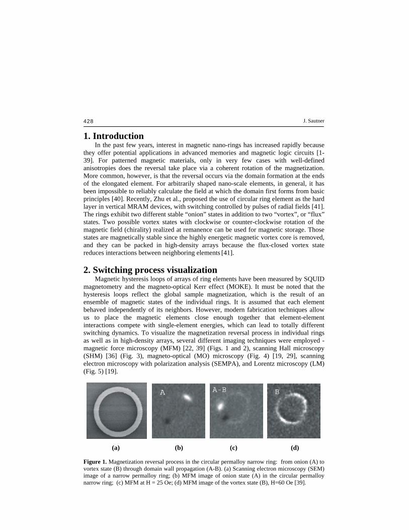
4. Two onion states at remanence in square nano-wire elements as binary 1 and 0 In square rings, the domain wall can be trapped at the corners, similar to zig–zag nanowires. This will overcome the problem of movement of domain walls due to the effect of changing stray fields from the neighboring elements during selective writing. Preliminary studies indicate that the domain wall patterns and switching mechanism itself are controllable by the magnetic field strength and direction. A flux-closure structure is the energetically stable state in square-shaped magnetic elements. Even if the element is patterned into nanowires (square rings), the vortex state is still the energetically favorable state as it has the lowest magnetostatic energy. For narrow nanowires, after applying the magnetic field H along the diagonal of the square, the magnetization aligns at 45° to H forming the onion state at remanence, and the magnetization is reduced to 1/√2 from its saturated value (Fig. 9c). Micromagnetic simulations of a square ring structure confirm this [53-55]. However, other domain patterns exist depending on the magnetic history. If a large magnetic field is applied parallel to the edges, the element is magnetized into a single domain state, as shown in Fig. 9a. The domain walls are formed as the magnetic field is reduced to zero, which is shown in Fig. 9b. At the four corners, the magnetic moments gradually rotate by 90 deg. In addition to these domain walls, two transverse domain walls are formed in the middle of two of the nanowire segments that are perpendicular to the field directions. On both sides of the transverse domain walls, the magnetic moments are head-to-head or tail-to-tail domain walls. Such types of domain walls have recently been observed in zigzag patterned Co wires [56]. If, however, the magnetic field is slightly misaligned with respect to the edge direction, the domain patterns at remanence will be different. The applied field in the simulations is
(a) (b) (c)
Figure 9. In square rings, the domain wall can be trapped at the corners: (a) When a large magnetic field, higher than the saturation field, is applied parallel to the edge direction, the element is magnetized into a single domain state. Arrows show the direction of applied field; (b) Remanent state after applying a magnetic field exactly along the edge of the square nano-wire element; (c) The applied field in the micromagnetic simulations is applied at 2° up from the edge direction (100). The resulting remanent state is the “onion” state. After [53-54].

J. Sautner 436
applied at 2° from the edge directions in order to simulate the experimental results where perfect alignment is unlikely to be achieved. Fig. 11d shows the remanent magnetic state. At two opposite corners, the magnetic moments gradually rotate by 90 deg. At the other two diagonal corners, the magnetic moments form transverse domain walls. The stray field contrast of the z-component is higher at those locations and can be seen clearly as one white spot and one black spot at diagonal corners (Fig. 11a and Fig. 11d) [53]. Micromagnetic simulations and experimental results (Fig. 10) suggest that each of the four segments of the square shaped nanowires is nearly a single domain state, as indicated by white arrows in Fig. 10 (a-e). Different orientations of these single domain states form different domain patterns. The orientation of the moment states in these four segments can be controlled by the local magnetic fields. Figure 10a shows the magnetic moment state of a typical element at remanence. All the images have one black spot and one white spot at the corners. When the local magnetic field reaches the value of the domain wall pinning potential of the corner, it can move the domain wall from one corner to another corner. Figures 10b and 10c show such
(d) (e) (f)
Figure 10. MFM images at remanence of a single square nano-wire element after applying different magnetic fields. The magnetic field is applied approximately along the edge A of the square element. (a) Initial remanent state; (b) Metastable state called the 'horseshoe' state; (c) 90° onion state. A, B, C and D symbolize the four segments. White arrows in (a)-(c) indicate the magnetic moment orientation in each segment; (d) The micromagnetic simulations of the onion state in Fig (a); (e) The micromagnetic simulations of the horseshoe state. This state would correspond to the magnetic states in Fig. (b); (f) The micromagnetic simulations of the onion state in Fig (c).

Vortices in magnetic nano-rings 437
(a) (b) (c) (d)
Figure 11. MFM images at remanence of a single square nano-wire element after applying negative magnetic fields. The magnetic field is applied at 2-4° off from the edge of the square element. (a) Remanent state, similar to the state at Fig. 10e; (b) -163 Oe; (c) -196 Oe; (d). -256 Oe [37-38]. processes. In Fig. 10b, the segment A is switched, and that triggers the segment C to switch as well in Fig. 10c. If an opposite magnetic field is applied, similar phenomena occur, as shown in Fig. 11. It is obvious that the switching in this case is determined by the shape of the element and by the direction of the field. With the field applied along the edge, the intermediate state is a new bi-domain state, or “horseshoe” state. No nucleation or annihilation of the vortex state is required, and the switching is extremely simple and robust. This mechanism is a simple propagation of head-to-head and tail-to-tail domain walls along the wire from one corner to another corner of square nano-wire elements. A similar switching mechanism was observed by applying the component of the magnetic field perpendicular to the initial onion state. 5. Control of magnetic vortex chirality in asymmetric square rings Controlling the direction of domain wall movement and thus the switching process can be done by the introduction of asymmetries in the square ring structures. These asymmetries can include width gradients, notches, or slits, among others. It has been found that the switching mechanism strongly depends on the position of the introduced shape asymmetry (width gradient or slit) and the field orientation. The OOMMF simulations predicts that the switching can occur in two different ways, one characterized by the appearance of a vortex state, the other process going through an intermediate “horseshoe” state without vortex formation. Thus, it is possible to predict the cases of magnetic field and sample arrangement when a vortex state with a known chirality is created in our rings. Furthermore, it is possible to prescribe a procedure to write in a vortex with a given chirality by controlling the direction of the applied field. Understanding the switching and predicting the switching order of the branches in asymmetric square rings is a key issue of building the controllable magnetic elements for MRAM. 6. Vortex state in triangular magnetic nano-rings In addition to the square ring, triangular ring elements have been investigated as a magnetic layer in spintronic devices (Fig. 13). An important feature of this geometry is

J. Sautner 438
(a) (b) (c) (d) (e)
Figure 12. The direction of domain wall movement in the square ring structures: (a) In-field Lorentz image of a 980nm permalloy ring just before switching into the vortex state; Lorentz image of the vortex state; (c) Asymmetric square ring and ring with 50nm slit; (d) Square ring and ring with 50nm slit in one corner; (e) First order D-MOKE hysteresis curve (it is a Fourier component of magnetization) for the sample in (d) [57].
(a) Figure 13. The typical magnetic states of triangular ring element: (a) The MFM images of the magnetization configuration in a triangular ring; (b) Schematic presentation of those states as a function of in-plane field [60]. Note that the chirality of a vortex state changes sign when the magnetic field is swept to the opposite direction; (c-e) SEMPA images of vortex (c) and (e) and polarized (d) states. that the direction of domain wall movement can be controlled without the introduction of artificial shape asymmetries, such as notches or gaps [57], which are difficult to obtain with the required precision using conventional nanofabrication techniques. That makes the triangular ring geometry very suitable for size reduction, while retaining the capability of precise control over the direction of domain wall propagation [58-60]. Square and triangular nano-wire elements can be easily scaled down from the current 1 µm to submicron dimensions, as it was demonstrated earlier for circular ring elements [61]. Fig. 13 shows the typical magnetic states of triangular ring elements measured by MFM [60] and by SEMPA [62] (Fig. 13c-e).

Vortices in magnetic nano-rings 439
It is important to mention that the triangular ring geometry requires less activation for domain wall movement in comparison with the notched structures, and the current values required to de-pin and move the domain wall should be smaller. At the same time, the pinning potential for the domain walls introduced by the ring corners is stronger than pinning due to narrower, thinner and better edge-profiled contacts. Although a variety of different magnetic nano-elements have been studied, triangular ring magnetic elements, surprisingly, remain unexplored.
(a) (b)
Figure 14. In the real nanomagnetic structures the contacts should be both at the bottom and on the top of each structure. Unless complicated and expensive fabrication processes are used, this means that the magnetic structures are not flat and the switching mechanism and the switching field values could be affected. Magnetoresistive (MR) behavior will be different for individual elements in two cases: (a) The contacts under the ring (non-flat, 3-D); (b) Contacts on the top (flat) configurations. 7. Problem of integration of magnetic nano-rings into functional nanodevices
MRAM combines a magnetic device with standard silicon-based electronics to obtain non-volatility, high-speed operation, high density, and unlimited read and write capability [63]. MRAM cells are designed to have two stable magnetic states that correspond to high or low resistance values and retain those values without any applied power. The cells are read by sensing the resistance to determine if the state is high or low and the writing could be done by the magnetic fields generated from the current flowing in the bit and word lines [63, 64].
An alternative approach to selectively write in MRAM cells i.e. switch the magnetization of the soft layer in the current-perpendicular-to-plane (CPP) layered magnetic nanostructure was proposed by Slonczewski and Berger [65,66], and was based on the spin torque by a spin polarized current flowing through the magnetic nanostructure. The results demonstrated the switching of layer magnetization by applying a spin-polarized current [67] and provided a clear confirmation that spin transfer occurs in current-perpendicular-to-plane (CPP) spin valves and magnetic tunnel junctions (MTJ) [68-76]. The results show that the magnetic layer can be switched between the parallel and the antiparallel states by applying current densities of the order of 107 A/cm2. Recent results
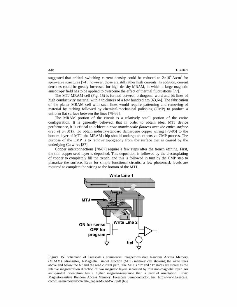
J. Sautner 440
suggested that critical switching current density could be reduced to 2×10⁶ A/cm2 for spin-valve structures [74], however, those are still rather high currents. In addition, current densities could be greatly increased for high density MRAM, in which a large magnetic anisotropy field has to be applied to overcome the effect of thermal fluctuations [77]. The MTJ MRAM cell (Fig. 15) is formed between orthogonal word and bit lines of high conductivity material with a thickness of a few hundred nm [63,64]. The fabrication of the planar MRAM cell with such lines would require patterning and removing of material by etching followed by chemical-mechanical polishing (CMP) to produce a uniform flat surface between the lines [78-86]. The MRAM portion of the circuit is a relatively small portion of the entire configuration. It is generally believed, that in order to obtain ideal MTJ device performance, it is critical to achieve a near atomic-scale flatness over the entire surface area of an MTJ. To obtain industry-standard damascene copper wiring [78-86] to the bottom layer of MTJ, the MRAM chip should undergo an expensive CMP process. The purpose of the CMP is to remove topography from the surface that is caused by the underlying Cu wires [87]. Copper interconnections [78-87] require a few steps after the trench etching. First, the thin copper seed layer is deposited. This deposition is followed by the electroplating of copper to completely fill the trench, and this is followed in turn by the CMP step to planarize the surface. Even for simple functional circuits, a few photomask levels are required to complete the wiring to the bottom of the MTJ.
Figure 15. Schematic of Freescale’s commercial magnetoresistive Random Access Memory (MRAM) 1-transistor, 1-Magnetic Tunnel Junction (MTJ) memory cell showing the write lines above and below the bit and the read current path. The MTJ’s “0” and “1” states are stored as the relative magnetization direction of two magnetic layers separated by thin non-magnetic layer. An anti-parallel orientation has a higher magneto-resistance than a parallel orientation. From: Magnetoresistive Random Access Memory, Freescale Semiconductor, Inc. http://www.freescale. com/files/memory/doc/white_paper/MRAMWP.pdf [63]

Vortices in magnetic nano-rings 441
If we can substantially reduce or, at least predict the influence of the surface modulation induced by the contact lines in the area of the MTJ, it would substantially reduce cost and prototyping turnaround time [87,88]. This would eliminate the need for CMP, and the expensive resources necessary for its application. However, our initial results strongly indicate that the geometry of the contact lines strongly influences the possible magnetic states, alters the switching mechanism, and leads to totally new behavior which was not observed in classic 2-D thin film magnetic structures [89, 90]. If the effects of magnetocrystalline anisotropy are negligible, only geometry determines the microscopic spin structure of the magnetic states. Until now, the main effort in magnetoelectronics has been concentrated on optimization of the 2-D shape of the magnetic layer(s). No one has mentioned, however, that those perfect “flat” multilayer ring structures are as far from real device geometry as any other proposed design. Because our goal is to shrink the size of our spintronic devices to dimensions comparable to CMOS transistors, or even smaller, the contact lines under the magnetic layer should be scaled down as well. Here they tend to lose definition, which makes them even rougher [91]. We could spend years trying to find “the best” design of magnetic layers fabricated on flat Si wafers, only to find out later that the surface modulation by contacts changes the switching mechanism. We are all competing with CMOS, trying to prove that our technology is better, faster, non-volatile, more reliable etc., and we are very reluctant to admit that spintronics is facing the same challenges as CMOS. We are all in the same boat- our circuits can no longer be considered in the classic 2-D approach of discrete lines passing through a circuit [91]. They should be considered 3-D, particularly where the roughness and shape of the contact lines influences performance to such extent that they modify the mechanism of operation. This 3-D problem was beautifully illustrated in “The Persistence of Memory”, probably the most famous painting by artist Salvador Dalí (Fig. 16). This well-known surrealistic painting introduced the image of the soft melting watch, which for us, symbolizes the problem of the magnetic element (watch) fabricated on top of a contact line (table), and conformally covering the contact line. In comparison with CMOS, the problem of the surface modulation of the magnetic element is even more exacerbated, because the thickness of magnetic layer(s) is in the range of a few nanometers [92], and could be only a fraction of the thickness of the contact lines. Some reduction of non-planarity could be achieved by reduction of contact line thicknesses to fewer than 20nm, compared to conventional thicknesses of approximately 100-300nm. However, that would lead to the drastic reduction in the current carrying ability of the contact line in current-perpendicular-to-plane (CPP) configurations. In order for the MTJ MRAM device to be competitive, in terms of power consumption and device density with other forms of RAM, it is necessary that the MTJ be made very small, typically of sub-micron dimensions [93, 94]. Magnetic nanorings have been studied intensively because of their outstanding magnetic properties, which make them good candidates as building blocks for high density MRAM (Fig. 17) [41, 4-7, 34, 37, 95, 96]. Of particular interest is the formation of a magnetic flux closure state, called the vortex state (Fig. 17b), which characterizes the magnetization switching of circular elements (rings and discs) [41]. The interest arises from the fact that the magnetic configurations and the magnetization reversal mechanisms in these elements are markedly

J. Sautner 442
Figure 16. From Dali’s most famous painting “The Persistence of Memory”. insensitive to shape fluctuations and edge roughness. Moreover, the negligible magnetostatic interaction between the magnetic flux-closure vortex states of the rings or discs organized in arrays makes these systems appealing for high-density storage applications [41]. The main advantage of the ring geometry over other geometries is better control (viz., stability and reproducibility) of the remanent state and magnetization switching. For materials with small magnetocrystalline anisotropy, only the geometry determines the microscopic spin structure of the magnetic states. For instance, the effects of different geometrical constrictions, such as notches on domain walls in circular nanorings have been investigated [33,37]. These studies demonstrated the ability to control the domain wall motion and the formation of a vortex state through the introduction of ad-hoc constrictions or shape asymmetries. [33,37,97,98]. The application of such nanomagnets as device elements in magnetic recording mediums and MRAM requires a simple and reliable method for reading the stored information in the form of magnetization circulation (chirality). Among the methods applied for reading the stored information, the one which is the most likely candidate for practical applications is the use of magnetotransport measurements. Magnetoresistive measurements have indeed proven to be successful for retrieving information about the field dependence of magnetization configurations inside laterally confined systems when applied to both disks and rings. [33,97]. In this connection, another source of interest is the possibility, crucial for applications, to induce a controlled and reproducible domain wall displacement in nanoring structures by injection of current pulses [99]. In all previous investigations the contacts for injecting the current and for reading the voltage drop have been deposited on the top of the magnetic structures [100]. In real MRAM structures the contacts should be both at the bottom and on the top of each structure. Unless complicated and expensive fabrication

Vortices in magnetic nano-rings 443
(a) (b)
(c) (d) Figure 17. In real MRAM structures the contacts should be both at the bottom and on the top of each structure: (a) Schematics of the vertical MRAM with bit line current flowing perpendicular to the element. Fig. 17a is from: J.-G. Zhu, Y. Zheng, and G. A. Prinz, Ultrahigh density vertical magnetoresistive random access memory, J. Appl. Phys. 87, 6668 (2000) [41]; Fig. 17b. The micromagnetic simulations of the flux closure or “vortex” state; Fig. 17c is SEM image and Fig. 17d is schematic drawing of our Co5nm/Cu3nm/FeNi5nm rings fabricated on top of 25nm thick Au contacts for CIP magneto-transport measurements. processes are used, the magnetic structure is a 3-D structure [87, 93]. The “non-flatness” of the magnetic element can substantially affect the magnetic behavior and functionality of the device [101]. 8. Non-flat circular magnetic rings Vavassori at al., found recently that the non-flatness of the magnetic structures affect profoundly the magnetic and the magnetoresistive behavior of the permalloy circular ring elements [92]. The rings investigated have an outer diameter of 1 µm and inner hole diameters of 150, 300, and 600nm. The 25nm thick permalloy (FeNi) rings have been lithographically patterned on four 25nm thick Au contacts, previously fabricated on a SiO2/Si substrate. For Au contact fabrication authors employed single-layer e-beam resist

J. Sautner 444
and each Au contact line was 100nm wide and 25nm thick with two sharp edges and almost rectangular cross-section, as shown schematically in Fig. 18c. Figure 18a shows the scanning electron microscopy images of the final structures. The MR response of each structure is measured using a four-terminal technique as shown in Fig. 18a, while the magnetic field is applied in the plane. The voltage drop is measured between contacts V+ and V- shown in Fig. 18a. Figure 18b shows a schematic of the magnetization configurations
(a) (b)
(c)
Figure 18. The “non-flatness” of the magnetic structures affect profoundly the magnetic and the magnetoresistive behavior of the permalloy circular ring elements: (a) The scanning electron microscopy images of the permalloy rings fabricated on top of 25nm Au contacts; (b) Summary of the micromagnetic simulations for rings with different diameters of the inner hole; (c) Schematic of the ring structure used in the simulations. Taking into account that the ring structures on top of Au contacts are not flat (see Fig. 17(d)), the micromagnetic simulations were carried out with the 3D eXtensible Solver (Oxs) of OOMMF using bi-layer structures made of a ring of 25nm-thick FeNi interrupted by non-magnetic contacts overlapped by additional 25nm-thick FeNi elements [90].

Vortices in magnetic nano-rings 445
that develop during the reversal process as they are calculated with micromagnetic simulations using the Object Oriented Micromagnetic Framework (OOMMF) [102]. Vavassori, et al. measured experimentally the magnetoresistance of those 3-D magnetic ring structures deposited on top of Au contacts and compared the measurements with simulations [89]. The magnetoresitance was simulated: i) assuming a perfectly flat 2-D magnetic structure; ii) with the 3D eXtensible Solver (Oxs) of OOMMF, using a bi-layer structure shown in Fig. 18c, made of a ring of 25-nm-thick Py interrupted by non-magnetic contacts overlapped by 25-nm-thick Py elements. The magnetoresistance curves calculated using the two approaches differ considerably between them, and only those obtained using non-flat 3-D structures reproduce the experimental curves [89,90]. The results presented demonstrate that the non-planarity of the magnetic structures created by contacts with rectangular cross-sections of the same thickness as the magnetic material affect profoundly the magnetic and the magnetoresistive behavior of the rings. 9. Overview of 3-D Device Structures Based on Square Nano-rings As it was discussed earlier, in contrast to singly-connected magnetic dots, magnetic nano-rings can be readily set in several different magnetic states [4, 5, 19, 22, 29, 57, 103-105, 58-60]. In-field magnetic imaging shows that shape effects are crucial to understanding vortex formation and chirality in soft-magnetic elements [51,106,107]. Several methods have been proposed to control vortex rotation (chirality) and switching. Schneider et al. [106] demonstrated that vortex rotation in circular dots could be controlled by introducing a slight in-plane asymmetry to the circular shape. In a similar approach Kläui et al. [6] and Saitoh et al. [52] proposed controlling the direction of domain wall movement, and thus the switching process in rings by introducing a notch in the ring [6], or by using rings with an overall asymmetrical shape, respectively [52, 108]. For 1 µm Co, Ni, and permalloy square rings, Vavassori and his collaborators demonstrated the possibility of controllable switching from one stable “onion” state to another stable “onion” state by domain wall propagation, and that the exact location of the domain walls (DW) could be detected by in-plane manetoresistance measurements [61, 97]. Recently there have been investigations into the magnetization reversal in permalloy square rings with a narrow slit at one of the corners (Fig. 21a) and it was observed that head-to-head DWs can be positioned at selected corners and moved between corners by applying a small field [57]. The magnetoresistance in these structures is dominated by the anisotropic magnetoresistance [110] and a maximum resistance is observed when the spins are parallel or antiparallel to the injected current flow. This corresponds to a state when there is no DW present between the two sensing leads and the magnetization follows the direction of the pe rimeter of the ring. If a DW is present between the measuring leads, some of the magnetization of the DW points perpendicularly to the current flow and hence the resistance is lowered (Fig. 22). As a result, magnetoresistance could be used to determine the location of a DW [34, 89,90].

J. Sautner 446
(a) (b) (c)
(d) (e)
Figure 19a. In square ring elements, the head-to-head and tail-to-tail walls form at the opposite wire bends, and at two other corners, the magnetic moments gradually rotate by 90 degrees, separating almost single domain elements in adjacent segments: (a) The micromagnetic simulations of the “onion” state; (b) The intermediate “horseshoe” state; (c) The micromagnetic simulations of the vortex state; (d) Simulated MFM image of the ring in the vortex state; (e) Lorentz TEM image of the vortex states with clockwise (CW) chirality in 1µm permalloy square rings. Figure 20
(a) (b)

Vortices in magnetic nano-rings 447
(b) (d)
(e) Figure 20. In our preliminary work we demonstrated that the domain walls could be moved from one corner to another by a very small local magnetic field [99, 109]. In Fig. (a-d) black and white MFM contrast comes from the “stray” fields at domain wall locations in the corners [109]; (e) SEM image of permalloy square ring on top of Au contacts. Crucial for applications is the possibility to induce a controlled and reproducible DW displacement by injection of polarized current pulses rather than by using a magnetic field. [111] The current induced DW motion is due to a spin-torque effect, where the electrons transfer angular momentum to the DW when passing through it, pushing it in the direction of the electron flow [112-114]. It has recently been demonstrated that a DW in square ring structures can be reversibly and controllably displaced by current pulses alone [90].

J. Sautner 448
10. Fabrication of square nano-rings The 25nm thick permalloy square ring structures have been lithographically patterned on top of 20nm thick and 100nm wide Au contacts, previously fabricated on a SiO2/Si substrate. This time Au contacts were fabricated using double-layer e-beam resist which produces contact lines with more rounded edges in comparison with the single layer resist process. The outside size of the rings is 1.0µm × 1.0µm, the width of each segment is 150nm and the slit is 80nm wide. Fig. 21a shows the scanning electron microscopy image of the final structure. In the square rings head-to-head DWs can be pinned at the corners of the ring structure without requiring notches.
(a) (b)
(c) (d) Figure 21. Domain wall pinning in the corners of square nano rings. After [57, 90]. This geometry requires less activation in comparison to notch structure and proposed to study the current injection induced wall movement; (a) SEM image of permalloy square ring on top of Au contacts; (b) At sufficiently high currents the domain wall could be dragged by the current from State A (b) to state B (Fig. (c)); (d) The micromagnetic simulations of the state B assuming that the ring is completely flat with no influence from the contacts under the ring.

Vortices in magnetic nano-rings 449
It has been shown that by using current pulses with duration of 10 - 20µs and amplitude up to ± 5mA, which corresponds to current densities up to 2 × 10¹²A/m2 in the ring, the domain wall could be reversibly and controllably displaced by current pulses between the two corners (from state A to state B and from B to A, Fig. 21b-c). However, for smaller current densities of 1.6 × 10¹²A/m2 the transition between states A and B takes place through an intermediate metastable state - state C (sketched in Fig. 23a) corresponding to the DW being located in the area between contacts 2 and 3. It means that the surface modulation introduced by contacts 2 and 3 creates a pinning potential for the DW (Fig. 23b). As we discussed earlier in Section 8 for circular rings, the non- flatness of the magnetic structures may affect profoundly the magnetoresistance and switching in ring structures. Those results clearly indicate that it is not the pinning by the corners of the ring that determines the switching current densities, but rather topography induced by contact lines 2 and 3 (Fig. 24). It is surprising that it was possible to switch between states A and B at all. It can be attributed to the thinner and better edge profile of the Au contacts used here (double layer e-beam resist technology produces more rounded edges in comparison with the single layer resist fabrication (Section 8)). Example profiles
Figure 22. Top panel: measured MR signals between contacts 1 and 2 (solid dots) and 3 and 4 (open squares) of the square ring structure shown in Fig. 21(a). Bottom panel shows calculated MR signals between contacts 1-2 and 3-4 [90].

J. Sautner 450
(a) (b) Figure 23. For smaller currents the transition between states A (Fig. 21(b)) and B (Fig. 21(c)) takes place through an intermediate metastable state C (Fig. (a)), corresponding to the DW (bright red line) being located in the area between contacts 2 and 3 (Fig. b).
(a)
(b) Figure 24. SEMPA images of the top (a) and bottom (b) parts of permalloy ring, similar to shown in Fig. 21a. The yellow arrows indicate the direction of the local magnetization. Note the strong magnetization around the contacts.

Vortices in magnetic nano-rings 451
Figure 25. Different contact profiles could by fabricated: (a) by lift-off; (b) RIE; (c) Ar-milling. All those techniques are available in the NCF UIC. are illustrated in figure 25. It was found later that the repeated injection of high amplitude pulses damages the injection contact, although the integrity of the ring structure is preserved. To prevent damage to the contacts, it is necessary to either increase the contact thickness or change/reduce the surface modulation by contacts.
Conclusion Magnetoresistive random access memory offers the hope of being a low-cost, low-power, long-life, non-volatile memory solution for a variety of applications. Nanoscale MRAM is now a reality and magnetic nano-rings are a viable prospect for future generations of MRAM devices. Real MRAM devices are truly 3-dimensional structures. Their topography must absolutely be taken into consideration during the design phase since their inherent non-planarity will profoundly affect their magnetization profile. Additional work remains to be done to determine which ring geometry is appropriate for optimal device performance and ease of fabrication. Acknowledgements The information in this article has been compiled from many sources. The entire project has been possible thanks to the enthusiastic support, help, and advice of our colleagues J. Bekaert, G. H. Bernstein, J. De Boeck, K.S. Buchanan, Y. Bruynseraede, G. Crabtree, G. Csaba, M. Freeman, J.W. Freeland, M. Grimsditch, P. Grütter, A. Hoffmann, B. Ilic, A. Imre, B. Jankó, D.J. Keavney, V. V. Moshchalkov, P. Neuzil, V. Novosad, W. Porod, V. Rose, A. V. Silhanek, P. Vavassori, V. K. Vlasko-Vlasov, U. Welp, N. J. Zaluzec and Xiaobin Zhu. This work was supported by the U.S. National Science Foundation through Grant No. ECS-0202780 and by the U.S. Department of Energy, Basic Energy Science under Contract No. DE-AC02-06CH1357 (CNM 468, CNM 470 and GUP-8733).

J. Sautner 452
References 1. F. J. Castaño, C. A. Ross, A. Eilez, W. Jung, and C. Frandsen, Magnetic configurations in
160–520-nm-diameter ferromagnetic rings, Phys. Rev. B 69, 144421 (2004) 2. V. Metlushko, U. Welp, V. Vlasko-Vlasov, G. Crabtree, N. Zaluzec, J. Hiller, M. Grimsditch,
B. Ilic, J. Bekaert, V. Moshchalkov, Y. Bruynseraede, J. Das, J. De Boeck, G. Borghs, Xiaobin Zhu and P. Grutter, Arrays of nano-rings for magnetic storage applications, Proceedings of the 2002 2nd IEEE Conference on Nanotechnology, IEEE-NANO 2002, Page(s): 63 - 66
3. F. J. Castaño, C. A. Ross, C. Frandsen, A. Eilez, D. Gil, and Henry I. Smith, M. Redjdal and F. B. Humphrey, Metastable states in magnetic nanorings, Phys. Rev. B 67, 184425 (2003)
4. J. Rothman, M. Kläui, L. Lopez-Diaz, C. A. F. Vaz, A. Bleloch, J. A. C. Bland, Z. Cui, and R. Speaks, Observation of a bi-domain state and nucleation free switching in mesoscopic ring magnets, Phys. Rev. Lett. 86, 1098 (2001)
5. S. P. Li, D. Peyrade, M. Natali, A. Lebib, Y. Chen, U. Ebels, L. D. Buda, and K. Ounadjela, Flux closure structures in cobalt rings, Phys. Rev. Lett. 86, 1102 (2001)
6. M. Kläui, J. Rothman, L. Lopez-Diaz, C. A. F. Vaz, J. A. C. Bland, Z. Cui, Vortex circulation control in mesoscopic ring magnets, Appl.Phys. Lett. 78, 3268 (2001)
7. T. Uhlig, and J. Zweck, Direct Observation of Switching Processes in Permalloy Rings with Lorentz Microscopy, Phys. Rev. Lett. 93, 047203 (2004)
8. Xiaoyong Liu, D. Mazumdar, B. D. Schrag, W. Shen, and Gang Xiao, Magnetization reversal of submicrometer Co rings with uniaxial anisotropy via scanning magnetoresistance microscopy, Phys. Rev. B 70, 014407 (2004)
9. D. R. Lee, J. W. Freeland, G. Srajer, V. Metlushko, Chun-Yeol You, Domain-specific magnetization reversals on a Permalloy square ring array, J. Appl. Phys. 95, 7016 (2004)
10. C. A. F. Vaz, M. Kläui, J. A. C. Bland, L. J. Heyderman, F. Nolting, Effect of the magnetocrystalline anisotropy on the magnetic behavior of ring element, J. Appl. Phys. 95, 6732 (2004)
11. Yung Liou, Dong-Cheng Chen, Chwen Yu, J. S. Chen, Shang-Fan Lee, Y. D. Yao, C. C. Tzeng, T. Y. Chen, K. W. Cheng and Ron Ma, Magnetic switching and reversal process in a tip ring structure, J. Appl. Phys. 95, 6723 (2004)
12. Wentao Xu, D. B. Watkins, L. E. DeLong, K. Rivkin, J. B. Ketterson, V. Metlushko, Ferromagnetic resonance study of nanoscale ferromagnetic ring lattices, J. Appl. Phys. 95, 6645 (2004)
13. M. Kläui, C. A. F. Vaz, J. A. C. Bland, L. J. Heyderman, C. David, E. H. C. P. Sinnecker, and A. P. Guimarães, Multistep switching phase diagram of ferromagnetic ring structures, J. Appl. Phys. 95, 6639 (2004)
14. Z. B. Guo, Y. K. Zheng, K. B. Li, Z. Y. Liu, P. Luo, Y. H. Wu, Asymmetrically kinked hysteresis loops in exchange biased NiFe/IrMn rings, J. Appl. Phys. 95, 4918 (2004)
15. F. J. Castaño, C. A. Ross, A. Eilez, W. Jung, and C. Frandsen, Magnetic configurations in 160–520-nm-diameter ferromagnetic rings, Phys. Rev. B 69, 144421 (2004)
16. M. Kläui, C. A. F. Vaz, J. A. C. Bland, E. H. C. P. Sinnecker, A. P. Guimarães, W. Wernsdorfer, G. Faini, E. Cambril, L. J. Heyderman and C. David, Switching processes and switching reproducibility in ferromagnetic ring structures, Appl. Phys. Lett. 84, 951 (2004)
17. M. Steiner and J. Nitta, Control of magnetization states in microstructured permalloy ring, Appl. Phys. Lett. 84, 939 (2004)
18. M. Kläui C. A. F. Vaz, J. A. C. Bland, T. L. Monchesky, J. Unguris, E. Bauer, S. Cherifi, S. Heun, and A. Locatelli, L. J. Heyderman, Z. Cui, Direct observation of spin configurations and classification of switching processes in mesoscopic ferromagnetic rings, Phys. Rev. B 68, 134426 (2003)
19. U. Welp, V. K. Vlasko-Vlasov, J. M. Hiller, N. J. Zaluzec, V. Metlushko, B. Ilic, Magnetization reversal in arrays of Co rings, Phys. Rev. B 68, 054408 (2003)

Vortices in magnetic nano-rings 453
20. M. Kläui, C. A. F. Vaz, J. A. C. Bland, W. Wernsdorfer, G. Faini, E. Cambril, L. J. Heyderman, Domain wall motion induced by spin polarized currents in ferromagnetic ring structures, Appl. Phys. Lett. 83, 105 (2003)
21. L. J. Heyderman, C. David, M. Kläui, C. A. F. Vaz, and J. A. C. Bland, Nanoscale ferromagnetic rings fabricated by electron-beam lithography, J. Appl. Phys. 93, 10011 (2003)
22. Xiaobin Zhu, P. Grütter, V. Metlushko, Y. Hao, F. J. Castaño, and C. A. Ross, B. Ilic, and H. I. Smith, Construction of hysteresis loops of single domain elements and coupled permalloy ring arrays by magnetic force microscopy, J. Appl. Phys. 93, 8540 (2003)
23. J. L. Tsai, Y. D. Yao, B. S. Han, S. F. Lee, C. Yu, T. Y. Chen, E. W. Huang, D. J. Zheng, Magnetoresistance and magnetic force microscopy studies in Ni80Fe20 disk- and ring-patterned wires, J. Appl. Phys. 93, 8424 (2003)
24. P. Vavassori, M. Grimsditch, V. Novosad, V. Metlushko, B. Ilic, Magnetization switching in Permalloy square ring magnets, J. Appl. Phys. 93, 7900 (2003)
25. M. Kläui, C. A. F. Vaz, J. A. C. Bland, W. Wernsdorfer, G. Faini and E. Cambril, Domain wall pinning and controlled magnetic switching in narrow ferromagnetic ring structures with notches (invited), J. Appl. Phys. 93, 7885 (2003)
26. C. Yu, S. F. Lee, Y. D. Yao, Y. R. Ma, E. W. Huang, J. L. Tsai, T. Y. Chen, C. R. Chang, Magnetoresistance study in NiFe semicircle-ring patterned wires, J. Appl. Phys. 93, 7619 (2003)
27. Mei-Feng Lai, Zung-Hang Wei, Ching-Ray Chang, J. C. Wu, W. Z. Hsieh, N. A. Usov, Jun-Yang Lai, Y. D. Yao, Magnetization patterns of permalloy square frames, J. Appl. Phys. 93, 7426 (2003)
28. W. L. Zhou, J. He, J. Fang, T.-A. Huynh, T. J. Kennedy, K. L. Stokes, and C. J. O'Connor, Self-assembly of FePt nanoparticles into nanorings, J. Appl. Phys. 93, 7340 (2003)
29. U. Welp, V. K. Vlasko-Vlasov, G. W. Crabtree, J. Hiller, and N. Zaluzec, V. Metlushko and B. Ilic, Magnetization reversal in arrays of individual and coupled Co-rings, J. Appl. Phys. 93, 7056 (2003)
30. F. J. Castaño, C. A. Ross, C. Frandsen, A. Eilez, D. Gil, Henry I. Smith, M. Redjdal and F. B. Humphrey, Metastable states in magnetic nanorings, Phys. Rev. B 67, 184425 (2003)
31. Y. G. Yoo, M. Kläui, C. A. F. Vaz, L. J. Heyderman, J. A. C. Bland, Switching field phase diagram of Co nanoring magnets, Appl. Phys. Lett. 82, 2470 (2003)
32. P. Vavassori, M. Grimsditch, V. Novosad, V. Metlushko, and B. Ilic, Metastable states during magnetization reversal in square permalloy rings, Phys. Rev. B 67, 134429 (2003)
33. M. Kläui, C. A. F. Vaz, J. Rothman, J. A. C. Bland, W. Wernsdorfer, G. Faini, and E. Cambril, Domain Wall Pinning in Narrow Ferromagnetic Ring Structures Probed by Magnetoresistance Measurements, Phys. Rev. Lett. 90, 097202 (2003)
34. Mei-Feng Lai, Zung-Hang Wei, Ching-Ray Chang, J. C. Wu, J. H. Kuo, and Jun-Yang Lai, Influence of vortex domain walls on magnetoresistance signals in Permalloy ring, Phys. Rev. B 67, 104419 (2003)
35. S. P. Li, W. S. Lew, J. A. C. Bland, M. Natali, A. Lebib, and Y. Chen, Intrinsic anisotropy-defined magnetization reversal in submicron ring magnets, J. Appl. Phys. 92, 7397 (2002)
36. J. Bekaert, D. Buntinx, C. Van Haesendonck, V. V. Moshchalkov, J. De Boeck, G. Borghs, and V. Metlushko, Noninvasive magnetic imaging and magnetization measurement of isolated mesoscopic Co rings, Appl. Phys. Lett. 81, 3413 (2002)
37. M. Kläui, C. A. F. Vaz, J. A. C. Bland, W. Wernsdorfer, G. Faini and E. Cambril, Controlled magnetic switching in single narrow rings probed by magnetoresistance measurements, Appl. Phys. Lett. 81, 108 (2002)
38. L. Lopez-Diaz, J. Rothman, M. Kläui, and J. A. C. Bland, Vortex formation in magnetic narrow rings: The role of magneto-crystalline anisotropy, J. Appl. Phys. 89, 7579 (2001)
39. Xiaobin Zhu, P. Grütter, V. Metlushko, and B. Ilic, “Magnetic structures and Magnetization reversal of patterned permalloy rings”, submitted to Phys. Rev. Lett.

J. Sautner 454
40. M. Grimsditch, A. Berger, J. Johnson, V. Metlushko, B. Ilic, P. Neuzil and R. Kumar, Magnetic stability of nano-particles: The role of dipolar instability pockets, Europhys. Lett., 54 , 813 (2001)
41. J. G. Zhu, Y.F. Zheng, and G.A.Prinz, Ultrahigh density vertical magnetoresistive random access memory, J.Appl.Phys. 87, 6668 (2000)
42. V. Metlushko, U.Welp, V.Vlasko-Vlasov, G.Crabtree, M. Grimsditch, V. Novosad, N. Zaluzec, B. Ilic, J. Bekaert, V. V. Moshchalkov, Y. Bruynseraede, J. De Boeck, G. Borghs, Xiaobin Zhu, P.Grütter, A. Imre, G. Csaba, G. H. Bernstein, and W. Porod, Nanomagnets: from nano-dots to nano-rings (Invited), Proceeding of International Conference on Electromagnetics in Advanced Applications, September 8-12, 2003 Torino, Italy
43. V. Metlushko, U.Welp, V.Vlasko-Vlasov, G.Crabtree, M. Grimsditch, V. Novosad, N. Zaluzec, B. Ilic, J. Bekaert, V. V. Moshchalkov, Y. Bruynseraede, J. De Boeck, G. Borghs, Xiaobin Zhu, P.Grütter, A. Imre, G. Csaba, G. H. Bernstein, and W. Porod, Vortex-vortex interactions in arrays of magnetic ring elements (Invited), Proceedings of European Conference on Vortex Matter in Superconductors at Extreme Scales and Conditions, September 20-28, 2003, Crete, Greece
44. R. D. McMichael and M. J. Donahue, Head to head domain wall structures in thin magnetic strips, IEEE Trans. Magn. 33, 4167 (1997).
45. http://math.nist.gov/oommf/software.html 46. P. Vavassori, M. Grimsditch, N. Zaluzec, V. Metlushko, and B. Ilic, Magneto-resistance of
single magnetic vortices, submitted to Appl. Phys. Let. 86, 072507 (2005) 47. M. Grimsditch, P. Vavassori, V. Novosad, V. Metlushko, H. Shima, Y. Otani, and K.
Fukamichi, Vortex chirality in an array of ferromagnetic dots, Phys. Rev. B 65, 172419 (2002) 48. Xiaobin Zhu, Z. Liu, M. Malac, Hui Qian, M. Freeman, V. Metlushko, B. Ilic, Magnetic
structure, magnetization reversal and spin dynamics of micron-sized permalloy ring, Annual APS March Meeting 2004, Montreal, Canada March 22-26, 2004
49. X. Zhu, Z. Liu, K. Buchanan, G. Woltersdorf, J. Liang, P. Grutter, V. Metlushko, A. Meldrum, J. Xu, B. Heinrich, and M. Freeman, Spin relaxation from continuous film to magnetic nanostructures, The International Conference on MEMS, NANO and Smart Systems (ICMENS 2004) Banff, Alberta, Canada, August 25 27, 2004
50. V. Metlushko, X. Zhu, Z. Liu, H. Qian, M. Malac, M. Freeman, Magnetic structure, magnetization reversal and spin dynamics of micron-sized permalloy rings, 49th Conference on Magnetism & Magnetic Materials (MMM’04), November 7-11, Jacksonville, FL, 2004
51. M. Schneider, H. Hoffmann, and J. Zweck, Magnetic switching of single vortex permalloy elements, Appl. Phys. Lett. 79, 3113 (2001)
52. E. Saitoh, M. Kawabata, K. Harii, H. Miyajima, and T. Yamaoka, Manipulation of vortex circulation in decentered ferromagnetic nanorings, J. Appl. Phys. 95, 1986 (2004)
53. Xiaobin Zhu, P. Grutter, V. Metlushko, B. Ilic, Control of domain wall patterns in square shaped nickel nanowires, Proceedings of 47th Annual Conference on Magnetism & Magnetic Materials, Tampa, FL, November 11-15, 2002
54. V. Metlushko; X. Zhu; B. Ilic; P. Grutter, Magnetic structure and magnetization reversal of circular and square shaped nanowire arrays, Proceedings of 47th Annual Conference on Magnetism & Magnetic Materials, Tampa, FL, November 11-15, 2002
55. P. Vavassori, M. Grimsditch, V. Novosad, V. Metlushko, B. Ilic, Magnetization switching in permalloy square ring magnets, Proceedings of 47th Annual Conference on Magnetism & Magnetic Materials, Tampa, FL, November 11-15, 2002
56. T. Taniyama, I. Nakatani, T. Yakabe, Y. Yamazaki, Control of domain structures and magnetotransport properties in patterned ferromagnetic wires, Appl. Phys. Lett. 76, 613 (2000).
57. A. Libál, M. Grimsditch, V. Metlushko, P. Vavassori, and B. Jankó, Control of magnetic vortex chirality in square ring micromagnets, J. Appl. Phys. 98, 083904 (2005)

Vortices in magnetic nano-rings 455
58. P. Vavassori, O. Donzelli, M. Grimsditch, V. Metlushko, and B. Ilic, Chirality and stability of vortex state in Permalloy triangular ring micromagnets, J. Appl. Phys. 101, 023902 (2007)
59. A. V. Silhanek, W. Gillijns, V. V. Moshchalkov, V. Metlushko, and B. Ilic, Tunable pinning in superconducting films with magnetic microloops, Appl. Phys. Lett. 89, 182505 (2006)
60. A. Imre, E. Varga, L.L. Ji, B. Ilic, V. Metlushko, G. Csaba, A. Orlov, G. H. Bernstein, W. Porod, Flux-closure magnetic states in triangular cobalt ring elements, IEEE Trans. Mag. 42, 3641 (2006)
61. P. Vavassori, R. Bovolenta, V. Metlushko, and B. Ilic, Vortex rotation control in permalloy disks with small circular voids, J. Appl. Phys. 99, 053902 (2006)
62. A.V. Silhanek, W. Gillijns, V.V. Moshchalkov, V. Metlushko, F. Gozzini, B. Ilic, W. C. Uhlig, and J. Unguris, Manipulation of the vortex motion in nanostructured ferromagnetic/superconductor hybrids, Appl. Phys. Lett. 90, 182501 (2007)
63. http://www.freescale.com/files/memory/doc/white_paper/MRAMWP.pdf 64. S. A. Wolf, A. Y. Chtchelkanova, and D. M. Treger, Spintronics - A retrospective and
perspective, IBM Journal of Research and Development 50, 101 (2006) 65. J. C. Slonczewski, Current-driven excitation of magnetic multilayers, J. Magn. Magn. Mater.
159, L1 (1996). 66. L. Berger, Emission of spin waves by a magnetic multilayer traversed by a current, Phys. Rev.
B 54, 9353 (1996) 67. J. A. Katine, F. J. Albert, E. B. Myers, D. C. Ralph, and R. A. Buhrman, Current-driven
magnetization reversal and spin-wave excitations in Co/Cu/Co pillars, Phys. Rev. Lett. 84, 3149 (2000)
68. F. J. Albert, J. A. Kattine, R. A. Buhrman, and D. C. Ralph, Spin-polarized current switching of a Co thin film nanomagnet, Appl. Phys. Lett. 77, 3809 (2000)
69. J. Grollier, V. Gros, A. Hamzic, J. M. George, H. Jaffes, A. Fert, G. Faini, J. Ben Youssef, and H. Le Gall, Spin-polarized current induced switching in Co/Cu/Co pillars, Appl. Phys. Lett. 78, 3663 (2001)
70. Y. W. Liu, Z. Z. Zhang, P. P. Freitas, and J. L. Martins, Current-induced magnetization switching in magnetic tunnel junctions, Appl. Phys. Lett. 82, 2871 (2003)
71. Y. Huai, F. Albert, P. Nguyen, M. Pakala, and T. Valet, Observation of spin-transfer switching in deep submicron-sized and low-resistance magnetic tunnel junctions, Appl. Phys. Lett. 84, 3118 (2004)
72. G. D. Fuchs, N. C. Emley, I. N. Krivorotov, P. M. Braganca, E. M. Ryan, S. I. Kiselev, J. C. Sankey, D. C. Ralph, and R. A. Buhrman, Spin-transfer effects in nanoscale magnetic tunnel junctions, Appl. Phys. Lett. 85, 1205 (2004)
73. Y. Jiang, S. Abe, T. Ochiai, T. Nozaki, A. Hirohata, N. Tezuka, and K. Inomata, Effective reduction of critical current for current-induced magnetization switching by a Ru layer insertion in an exchange-biased spin valve, Phys. Rev. Lett. 92, 167204 (2004)
74. Y. Jiang, T. Nozaki, S. Abe, T. Ochiai, A. Hirohata, N. Tezuka, and K. Inomata, Substantial reduction of critical current for magnetization switching in an exchange-biased spin valve, Nat. Mater. 3, 361 (2004)
75. H. Meng, J. G. Wang, Z. T. Diao, and J. P. Wang, Low resistance spin-dependent magnetic tunnel junction with high breakdown voltage for current-induced-magnetization-switching devices, J. Appl. Phys. 97, 10C926 (2005)
76. H. Meng, J. Wang, and J.-P. Wang, Low critical current for spin transfer in magnetic tunnel junctions, Appl. Phys. Lett. 88, 082504 (2006)
77. J. Z. Sun, Spin-current interaction with a monodomain magnetic body: A model study, Phys. Rev. B 62, 570 (2000)
78. D. C. Edelstein, G. A. Sai-Halasz, and Y.-J. Mii, VLSI On-Chip Interconnection Performance Simulations and Measurements, IBM J. Res. Develop. 39, 383 (1995).

J. Sautner 456
79. D. C. Edelstein, Advantages of Copper Interconnects, Proceedings of the 12th International IEEE VLSI Multilevel Interconnection Conference, 1995, p. 301.
80. B. Luther, J. F. White, C. Uzoh, T. Cacouris, J. Hummel, W. Guthrie, N. Lustig, S. Greco, N. Greco, S. Zuhoski, P. Agnello, E. Colgan, S. Mathad, L. Saraf, E. J. Weitzman, C. K. Hu, F. Kaufman, M. Jaso, L. P. Buchwalter, S. Reynolds, C. Smart, D. Edelstein, E. Baran, S. Cohen, C. M. Knoedler, J. Malinowski, J. Horkans, H. Deligianni, J. Harper, P. C. Andricacos, J. Paraszczak, D. J. Pearson, and M. Small, Planar Copper-Polyimide Back End of the Line Interconnections for ULSI Devices, Proceedings of the 10th International IEEE VLSI Multilevel Interconnection Conference, 1993, p. 15.
81. P. C. Andricacos, Electroplated Copper Wiring on IC Chips, Interface 7, No. 1, 23 (1998). 82. M. Datta, R. V. Shenoy, C. Jahnes, P. C. Andricacos, J. Horkans, J. O. Dukovic, L. T.
Romankiw, J. Roeder, H. Deligianni, H. Nye, B. Agarwala, H. M. Tong, and P. Totta, Electrochemical Fabrication of Mechanically Robust PbSn C4 Interconnections, J. Electrochem. Soc. 142, 3779 (1995).
83. C.-K. Hu and J. M. E. Harper, Copper Interconnections and Reliability, Mater. Chem. Phys. 52, 5 (1998).
84. J. O. Dukovic and C. W. Tobias, Simulation of Leveling in Electrodeposition, J. Electrochem. Soc. 137, No. 12, 3748 (1990).
85. P. C. Andricacos, C. Uzoh, J. O. Dukovic, J. Horkans, and H. Deligianni, Damascene copper electroplating for chip interconnections, IBM J. Res. Develop. 42, 567 (1998)
86. J. O. Dukovic, Feature-Scale Simulation of Resist-Patterned Electrodeposition, IBM J. Res. Develop. 37, 125 (1993).
87. M. C. Gaidis, E. J. O’Sullivan, J. J. Nowak, Y. Lu, S. Kanakasabapathy, P. L. Trouilloud, D. C. Worledge, S. Assefa, K. R. Milkove, G. P. Wright, W. J. Gallagher, Two-level BEOL processing for rapid iteration in MRAM development, IBM J. Res. Develop. 50, 41 (2006)
88. D. W. Abraham, P. L. Trouilloud, and D. C. Worledge, Rapid-turnaround characterization methods for MRAM development, IBM J. Res. Develop. 50, 55 (2006)
89. P. Vavassori, A. Busato, A. Chiapatti, A. di Bona, S. Valeri, V. Metlushko, and B. Ilic, Effects of structural nonplanarity on the magnetoresistance of Permalloy circular rings, J. Appl. Phys. 101, 43901 (2007)
90. P.Vavassori, V. Metlushko, B. Ilic, Domain wall displacement by current pulses injection in submicrometer Permalloy square ring structures, Appl. Phys. Lett. 91, 093114 (2007)
91. http://www.semiconductor.net/article/CA499659.html 92. V. Rose, X.M. Cheng, D.J. Keavney, J.W. Freeland, K.S. Buchanan, B. Ilic, and V.
Metlushko, The breakdown of the fingerprinting of vortices by hysteresis loops in circular multilayer ring arrays, Appl. Phys. Lett. 91, 132501 (2007)
93. W. J. Gallagher, S. S. P. Parkin, Development of the magnetic tunnel junction MRAM at IBM: From first junctions to a 16-Mb MRAM demonstrator chip – References, IBM J. Res. Develop. 50, 5 (2006)
94. T. M. Maffitt, J. K. DeBrosse, J. A. Gabric, E. T. Gow, M. C. Lamorey, J. S. Parenteau, D. R. Willmott, M. A. Wood, and W. J. Gallagher, Design considerations for MRAM, IBM J. Res. Develop. 50, 25 (2006)
95. L. J. Heyderman, M. Kläui, B. Nöhammer, C. A. F. Vaz, J. A. C. Bland and C. David, Fabrication of nanoscale magnetic ring structures and devices, Microelectron. Eng. 73–74, 780 (2004).
96. D. Morecroft, F. J. Castaño, W. Jung, J. Feuchtwanger, and C. A. Ross, Influence of contact geometry on the magnetoresistance of elliptical rings, Appl. Phys. Lett. 88, 172508 (2006)
97. P. Vavassori, M. Grimsditch, V. Metlushko, N. Zaluzec, and B. Ilic, Magnetoresistance of single magnetic vortices, Appl. Phys. Lett. 86, 072507 (2005)

Vortices in magnetic nano-rings 457
98. M. Kläui, C. A. F. Vaz, J. A. C. Bland, and L. J. Heyderman, Domain wall coupling and collective switching in interacting mesoscopic ring magnet arrays, Appl. Phys Lett. 86, 032504 (2005).
99. D. Buntinx, A. Volodin, and C. Van Hasendonck, Influence of local anisotropic magnetoresistance on the total magnetoresistance of mesoscopic NiFe rings, Phys. Rev. B 70, 224405 (2004)
100. F. J. Castaño, D. Morecroft, W. Jung, and C. A. Ross, Spin-dependent scattering in multilayered magnetic rings, Phys. Rev. Lett. 95, 137201 (2005)
101. B. D. Schrag, A. Anguelouch, S. Ingvarsson, G. Xiao, Y. Lu, P. L. Trouilloud, A. Gupta, R. A. Wanner, W. J. Gallagher, P. M. Rice, and S. S. P. Parkin, Néel ‘orange peel’ coupling in magnetic tunneling junction devices, Appl. Phys. Lett. 77, 2373 (2000)
102. M. J. Donahue and D. G. Porter, OOMMF User's Guide, Version 1.2 alpha 3 (NIST, Gaithersburg MD, 2002)
103. P. Vavassori, M. Grimsditch, V. Novosad, V. Metlushko, and B. Ilic, Metastablestates during magnetization reversal in square permalloy rings, Phys. Rev. B 67, 134429 (2003)
104. X. Zhu, P. Grütter, V. Metlushko, and B. Ilic, Control of domain patterns in square shaped nickel rings, J. Appl. Phys. 93, 7059 (2003)
105. D. R. Lee, J. W. Freeland, G. Srajer, V. Metlushko, and Chun-Yeol You, Domain specific magnetization reversals on a Permalloy square ring array, J. Appl. Phys. 95, 7016 (2004)
106. M. Schneider, H. Hoffmann, and J. Zweck, Lorentz microscopy of circular ferromagnetic permalloy nanodisks, Appl. Phys. Lett. 77, 2909 (2000).
107. J. Raabe, R. Pulwey, R. Sattler, T. Schweinböck, J. Zweck, and D. Weiss, Magnetization pattern of ferromagnetic nanodisks, J. Appl. Phys. 88, 4437 (2000)
108. A. Subramani , D. Geerpuram , A. Domanowski , V. Baskaran and V. Metlushko Vortex state in magnetic rings, Physica C 404, 241 (2004)
109. P. Vavassori, N. Zaluzec, V. Metlushko, V. Novosad, B. Ilic, and M. Grimsditch, Magnetization reversal via single and double vortex states in submicron Permalloy ellipses, Phys. Rev. B 69, 214404 (2004)
110. T. R. McGuire and R. I. Potter, Anisotropic resistance in ferromagnetic 3d alloys, IEEE Trans. Magn. 11, 1018 (1975)
111. M. Kläui, C. A. F. Vaz, J. A. C. Bland, W. Wernsdorfer, G. Faini, E. Cambril, L. J. Heyderman, F. Nolting, and U. Rüdiger, Controlled and reproducible domain wall displacement by current pulses injected into ferromagnetic ring structures, Phys. Rev. Lett. 94, 106601 (2005)
112. L. Berger, Exchange interaction between ferromagnetic domain wall and electric current in very thin metallic films, J. Appl. Phys. 55, 1954 (1984)
113. G. Tatara and H. Kohno, Theory of current-driven domain wall motion: spin transfer versus momentum transfer, Phys. Rev. Lett. 92, 086601 (2004)
114. Thiaville, Y. Nakatani, J. Miltat, and N. Vernier, Domain wall motion by spin-polarized current: a micromagnetic study, J. Appl. Phys. 95, 7049 (2004)