Embed Size (px)
Citation preview
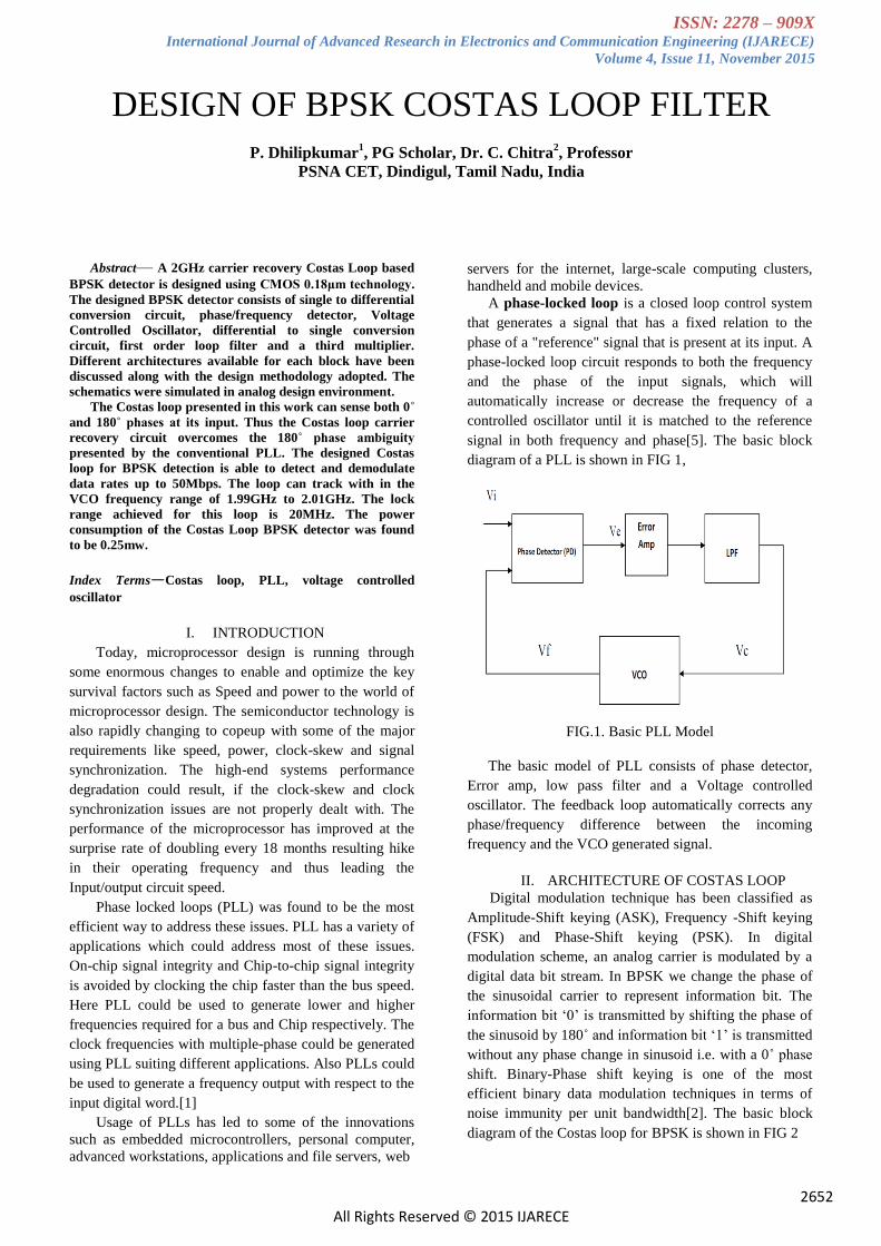
ISSN: 2278 – 909X International Journal of Advanced Research in Electronics and Communication Engineering (IJARECE)
Volume 4, Issue 11, November 2015
2652 All Rights Reserved © 2015 IJARECE
Abstract— A 2GHz carrier recovery Costas Loop based
BPSK detector is designed using CMOS 0.18μm technology.
The designed BPSK detector consists of single to differential
conversion circuit, phase/frequency detector, Voltage
Controlled Oscillator, differential to single conversion
circuit, first order loop filter and a third multiplier.
Different architectures available for each block have been
discussed along with the design methodology adopted. The
schematics were simulated in analog design environment.
The Costas loop presented in this work can sense both 0˚
and 180˚ phases at its input. Thus the Costas loop carrier
recovery circuit overcomes the 180˚ phase ambiguity
presented by the conventional PLL. The designed Costas
loop for BPSK detection is able to detect and demodulate
data rates up to 50Mbps. The loop can track with in the
VCO frequency range of 1.99GHz to 2.01GHz. The lock
range achieved for this loop is 20MHz. The power
consumption of the Costas Loop BPSK detector was found
to be 0.25mw.
Index Terms—Costas loop, PLL, voltage controlled
oscillator
I. INTRODUCTION
Today, microprocessor design is running through
some enormous changes to enable and optimize the key
survival factors such as Speed and power to the world of
microprocessor design. The semiconductor technology is
also rapidly changing to copeup with some of the major
requirements like speed, power, clock-skew and signal
synchronization. The high-end systems performance
degradation could result, if the clock-skew and clock
synchronization issues are not properly dealt with. The
performance of the microprocessor has improved at the
surprise rate of doubling every 18 months resulting hike
in their operating frequency and thus leading the
Input/output circuit speed.
Phase locked loops (PLL) was found to be the most
efficient way to address these issues. PLL has a variety of
applications which could address most of these issues.
On-chip signal integrity and Chip-to-chip signal integrity
is avoided by clocking the chip faster than the bus speed.
Here PLL could be used to generate lower and higher
frequencies required for a bus and Chip respectively. The
clock frequencies with multiple-phase could be generated
using PLL suiting different applications. Also PLLs could
be used to generate a frequency output with respect to the
input digital word.[1]
Usage of PLLs has led to some of the innovations
such as embedded microcontrollers, personal computer,
advanced workstations, applications and file servers, web
servers for the internet, large-scale computing clusters,
handheld and mobile devices.
A phase-locked loop is a closed loop control system
that generates a signal that has a fixed relation to the
phase of a "reference" signal that is present at its input. A
phase-locked loop circuit responds to both the frequency
and the phase of the input signals, which will
automatically increase or decrease the frequency of a
controlled oscillator until it is matched to the reference
signal in both frequency and phase[5]. The basic block
diagram of a PLL is shown in FIG 1,
FIG.1. Basic PLL Model
The basic model of PLL consists of phase detector,
Error amp, low pass filter and a Voltage controlled
oscillator. The feedback loop automatically corrects any
phase/frequency difference between the incoming
frequency and the VCO generated signal.
II. ARCHITECTURE OF COSTAS LOOP
Digital modulation technique has been classified as
Amplitude-Shift keying (ASK), Frequency -Shift keying
(FSK) and Phase-Shift keying (PSK). In digital
modulation scheme, an analog carrier is modulated by a
digital data bit stream. In BPSK we change the phase of
the sinusoidal carrier to represent information bit. The
information bit „0‟ is transmitted by shifting the phase of
the sinusoid by 180˚ and information bit „1‟ is transmitted
without any phase change in sinusoid i.e. with a 0˚ phase
shift. Binary-Phase shift keying is one of the most
efficient binary data modulation techniques in terms of
noise immunity per unit bandwidth[2]. The basic block
diagram of the Costas loop for BPSK is shown in FIG 2
DESIGN OF BPSK COSTAS LOOP FILTER
P. Dhilipkumar1, PG Scholar, Dr. C. Chitra
2, Professor
PSNA CET, Dindigul, Tamil Nadu, India
P. Dhilipkumar
1, PG Scholar, Dr. C. Chitra
2, Professor
PSNA CET, Dindigul, Tamil Nadu, India
ISSN: 2278 – 909X International Journal of Advanced Research in Electronics and Communication Engineering (IJARECE)
Volume 4, Issue 11, November 2015
2653 All Rights Reserved © 2015 IJARECE
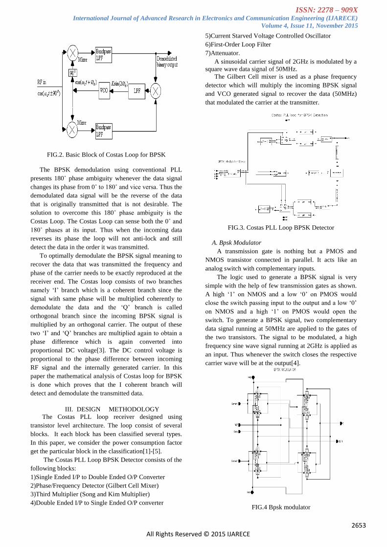
FIG.2. Basic Block of Costas Loop for BPSK
The BPSK demodulation using conventional PLL
presents 180˚ phase ambiguity whenever the data signal
changes its phase from 0˚ to 180˚ and vice versa. Thus the
demodulated data signal will be the reverse of the data
that is originally transmitted that is not desirable. The
solution to overcome this 180˚ phase ambiguity is the
Costas Loop. The Costas Loop can sense both the 0˚ and
180˚ phases at its input. Thus when the incoming data
reverses its phase the loop will not anti-lock and still
detect the data in the order it was transmitted.
To optimally demodulate the BPSK signal meaning to
recover the data that was transmitted the frequency and
phase of the carrier needs to be exactly reproduced at the
receiver end. The Costas loop consists of two branches
namely „I‟ branch which is a coherent branch since the
signal with same phase will be multiplied coherently to
demodulate the data and the „Q‟ branch is called
orthogonal branch since the incoming BPSK signal is
multiplied by an orthogonal carrier. The output of these
two „I‟ and „Q‟ branches are multiplied again to obtain a
phase difference which is again converted into
proportional DC voltage[3]. The DC control voltage is
proportional to the phase difference between incoming
RF signal and the internally generated carrier. In this
paper the mathematical analysis of Costas loop for BPSK
is done which proves that the I coherent branch will
detect and demodulate the transmitted data.
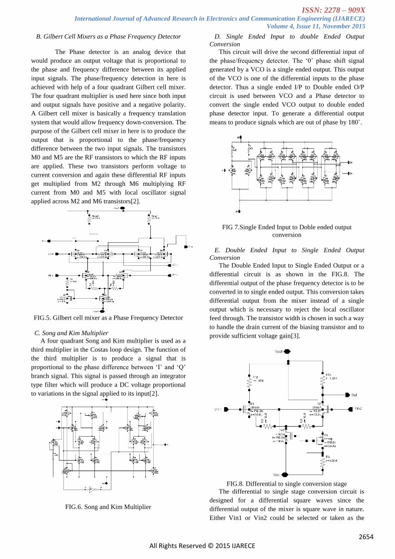
III. DESIGN METHODOLOGY
The Costas PLL loop receiver designed using
transistor level architecture. The loop consist of several
blocks. It each block has been classified several types.
In this paper, we consider the power consumption factor
get the particular block in the classification[1]-[5].
The Costas PLL Loop BPSK Detector consists of the
following blocks:
1)Single Ended I/P to Double Ended O/P Converter
2)Phase/Frequency Detector (Gilbert Cell Mixer)
3)Third Multiplier (Song and Kim Multiplier)
4)Double Ended I/P to Single Ended O/P converter
5)Current Starved Voltage Controlled Oscillator
6)First-Order Loop Filter
7)Attenuator.
A sinusoidal carrier signal of 2GHz is modulated by a
square wave data signal of 50MHz.
The Gilbert Cell mixer is used as a phase frequency
detector which will multiply the incoming BPSK signal
and VCO generated signal to recover the data (50MHz)
that modulated the carrier at the transmitter.
FIG.3. Costas PLL Loop BPSK Detector
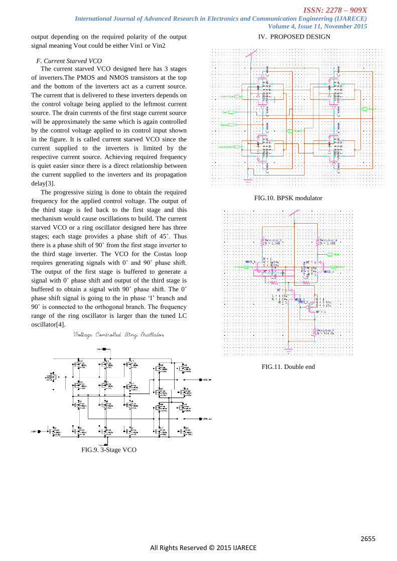
A. Bpsk Modulator
A transmission gate is nothing but a PMOS and
NMOS transistor connected in parallel. It acts like an
analog switch with complementary inputs.
The logic used to generate a BPSK signal is very
simple with the help of few transmission gates as shown.
A high „1‟ on NMOS and a low „0‟ on PMOS would
close the switch passing input to the output and a low „0‟
on NMOS and a high „1‟ on PMOS would open the
switch. To generate a BPSK signal, two complementary
data signal running at 50MHz are applied to the gates of
the two transistors. The signal to be modulated, a high
frequency sine wave signal running at 2GHz is applied as
an input. Thus whenever the switch closes the respective
carrier wave will be at the output[4].
FIG.4 Bpsk modulator
ISSN: 2278 – 909X International Journal of Advanced Research in Electronics and Communication Engineering (IJARECE)
Volume 4, Issue 11, November 2015
2654 All Rights Reserved © 2015 IJARECE
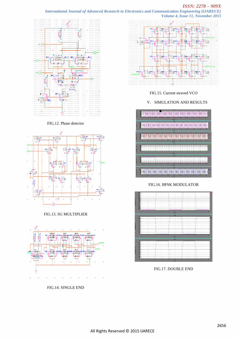
B. Gilbert Cell Mixers as a Phase Frequency Detector
The Phase detector is an analog device that
would produce an output voltage that is proportional to
the phase and frequency difference between its applied
input signals. The phase/frequency detection in here is
achieved with help of a four quadrant Gilbert cell mixer.
The four quadrant multiplier is used here since both input
and output signals have positive and a negative polarity.
A Gilbert cell mixer is basically a frequency translation
system that would allow frequency down-conversion. The
purpose of the Gilbert cell mixer in here is to produce the
output that is proportional to the phase/frequency
difference between the two input signals. The transistors
M0 and M5 are the RF transistors to which the RF inputs
are applied. These two transistors perform voltage to
current conversion and again these differential RF inputs
get multiplied from M2 through M6 multiplying RF
current from M0 and M5 with local oscillator signal
applied across M2 and M6 transistors[2].
FIG.5. Gilbert cell mixer as a Phase Frequency Detector
C. Song and Kim Multiplier
A four quadrant Song and Kim multiplier is used as a
third multiplier in the Costas loop design. The function of
the third multiplier is to produce a signal that is
proportional to the phase difference between „I‟ and „Q‟
branch signal. This signal is passed through an integrator
type filter which will produce a DC voltage proportional
to variations in the signal applied to its input[2].
FIG.6. Song and Kim Multiplier
D. Single Ended Input to double Ended Output
Conversion
This circuit will drive the second differential input of
the phase/frequency detector. The „0˚ phase shift signal
generated by a VCO is a single ended output. This output
of the VCO is one of the differential inputs to the phase
detector. Thus a single ended I/P to Double ended O/P
circuit is used between VCO and a Phase detector to
convert the single ended VCO output to double ended
phase detector input. To generate a differential output
means to produce signals which are out of phase by 180˚.
FIG 7.Single Ended Input to Doble ended output
conversion
E. Double Ended Input to Single Ended Output
Conversion
The Double Ended Input to Single Ended Output or a
differential circuit is as shown in the FIG.8. The
differential output of the phase frequency detector is to be
converted in to single ended output. This conversion takes
differential output from the mixer instead of a single
output which is necessary to reject the local oscillator
feed through. The transistor width is chosen in such a way
to handle the drain current of the biasing transistor and to
provide sufficient voltage gain[3].
FIG.8. Differential to single conversion stage
The differential to single stage conversion circuit is
designed for a differential square waves since the
differential output of the mixer is square wave in nature.
Either Vin1 or Vin2 could be selected or taken as the
ISSN: 2278 – 909X International Journal of Advanced Research in Electronics and Communication Engineering (IJARECE)
Volume 4, Issue 11, November 2015
2655 All Rights Reserved © 2015 IJARECE
output depending on the required polarity of the output
signal meaning Vout could be either Vin1 or Vin2
F. Current Starved VCO
The current starved VCO designed here has 3 stages
of inverters.The PMOS and NMOS transistors at the top
and the bottom of the inverters act as a current source.
The current that is delivered to these inverters depends on
the control voltage being applied to the leftmost current
source. The drain currents of the first stage current source
will be approximately the same which is again controlled
by the control voltage applied to its control input shown
in the figure. It is called current starved VCO since the
current supplied to the inverters is limited by the
respective current source. Achieving required frequency
is quiet easier since there is a direct relationship between
the current supplied to the inverters and its propagation
delay[3].
The progressive sizing is done to obtain the required
frequency for the applied control voltage. The output of
the third stage is fed back to the first stage and this
mechanism would cause oscillations to build. The current
starved VCO or a ring oscillator designed here has three
stages; each stage provides a phase shift of 45˚. Thus
there is a phase shift of 90˚ from the first stage inverter to
the third stage inverter. The VCO for the Costas loop
requires generating signals with 0˚ and 90˚ phase shift.
The output of the first stage is buffered to generate a
signal with 0˚ phase shift and output of the third stage is
buffered to obtain a signal with 90˚ phase shift. The 0˚
phase shift signal is going to the in phase „I‟ branch and
90˚ is connected to the orthogonal branch. The frequency
range of the ring oscillator is larger than the tuned LC
oscillator[4].
FIG.9. 3-Stage VCO
IV. PROPOSED DESIGN
FIG.10. BPSK modulator
FIG.11. Double end
ISSN: 2278 – 909X International Journal of Advanced Research in Electronics and Communication Engineering (IJARECE)
Volume 4, Issue 11, November 2015
2656 All Rights Reserved © 2015 IJARECE
FIG.12. Phase detector
FIG.13. SG MULTIPLIER
FIG.14. SINGLE END
FIG.15. Current straved VCO
V. SIMULATION AND RESULTS
FIG.16. BPSK MODULATOR
FIG.17. DOUBLE END
ISSN: 2278 – 909X International Journal of Advanced Research in Electronics and Communication Engineering (IJARECE)
Volume 4, Issue 11, November 2015
2657 All Rights Reserved © 2015 IJARECE
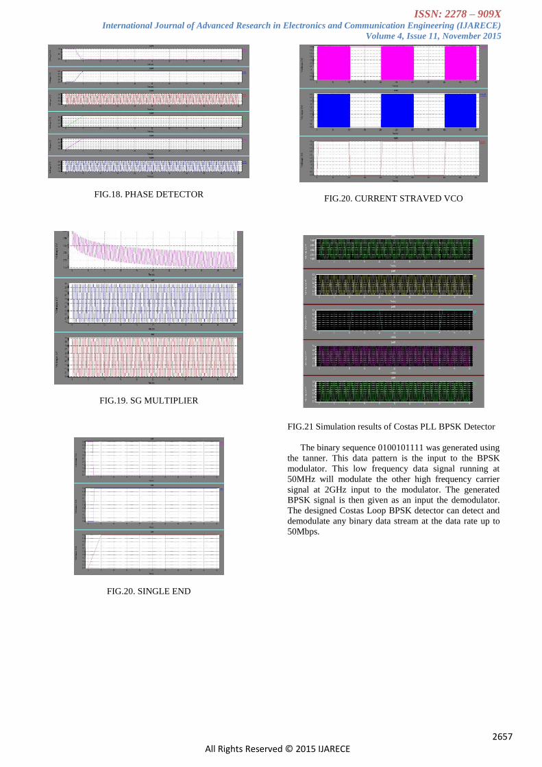
FIG.18. PHASE DETECTOR
FIG.19. SG MULTIPLIER
FIG.20. SINGLE END
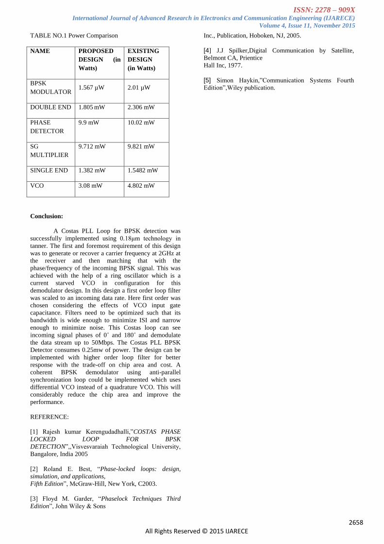
FIG.20. CURRENT STRAVED VCO
FIG.21 Simulation results of Costas PLL BPSK Detector
The binary sequence 0100101111 was generated using
the tanner. This data pattern is the input to the BPSK
modulator. This low frequency data signal running at
50MHz will modulate the other high frequency carrier
signal at 2GHz input to the modulator. The generated
BPSK signal is then given as an input the demodulator.
The designed Costas Loop BPSK detector can detect and
demodulate any binary data stream at the data rate up to
50Mbps.
ISSN: 2278 – 909X International Journal of Advanced Research in Electronics and Communication Engineering (IJARECE)
Volume 4, Issue 11, November 2015
2658 All Rights Reserved © 2015 IJARECE
TABLE NO.1 Power Comparison
NAME PROPOSED
DESIGN (in
Watts)
EXISTING
DESIGN
(in Watts)
BPSK
MODULATOR 1.567 µW 2.01 µW
DOUBLE END 1.805 mW 2.306 mW
PHASE
DETECTOR
9.9 mW 10.02 mW
SG
MULTIPLIER
9.712 mW 9.821 mW
SINGLE END 1.382 mW 1.5482 mW
VCO 3.08 mW 4.802 mW
Conclusion:
A Costas PLL Loop for BPSK detection was
successfully implemented using 0.18μm technology in
tanner. The first and foremost requirement of this design
was to generate or recover a carrier frequency at 2GHz at
the receiver and then matching that with the
phase/frequency of the incoming BPSK signal. This was
achieved with the help of a ring oscillator which is a
current starved VCO in configuration for this
demodulator design. In this design a first order loop filter
was scaled to an incoming data rate. Here first order was
chosen considering the effects of VCO input gate
capacitance. Filters need to be optimized such that its
bandwidth is wide enough to minimize ISI and narrow
enough to minimize noise. This Costas loop can see
incoming signal phases of 0˚ and 180˚ and demodulate
the data stream up to 50Mbps. The Costas PLL BPSK
Detector consumes 0.25mw of power. The design can be
implemented with higher order loop filter for better
response with the trade-off on chip area and cost. A
coherent BPSK demodulator using anti-parallel
synchronization loop could be implemented which uses
differential VCO instead of a quadrature VCO. This will
considerably reduce the chip area and improve the
performance.
REFERENCE:
[1] Rajesh kumar Kerengudadhalli,”COSTAS PHASE
LOCKED LOOP FOR BPSK
DETECTION”,,Visvesvaraiah Technological University,
Bangalore, India 2005
[2] Roland E. Best, “Phase-locked loops: design,
simulation, and applications,
Fifth Edition”, McGraw-Hill, New York, C2003.
[3] Floyd M. Garder, “Phaselock Techniques Third
Edition”, John Wiley & Sons
Inc., Publication, Hoboken, NJ, 2005.
[4] J.J Spilker,Digital Communication by Satellite,
Belmont CA, Prientice
Hall Inc, 1977.
[5] Simon Haykin,”Communication Systems Fourth
Edition”,Wiley publication.


![ISSN: 2278 909X International Journal of Advanced Research in …ijarece.org/wp-content/uploads/2017/05/IJARECE-VOL-6... · 2017-05-14 · McLean [3] derived relations for the minimum](https://img.pdfslide.us/doc/110x75/5ea04bb213d2e0694433d80b/issn-2278-909x-international-journal-of-advanced-research-in-2017-05-14-mclean.jpg)