Embed Size (px)
Citation preview

_.- - _
ISSCC97 I SESSION 8 I DATA CONVERTERS I PAPER FA 8.5
FA 8.5: A 2 . N 300MSamplels Track-and-Hold Amplifier
Andrew N. Karanicolas
Consultant, Morgenville, NJ
The growth of digital signal processing (DSP) applications drives higher sampling frequencies and resolutions for analog-to-digital converters (ADCs). At the same time, ADCs are required to operate from lower supply voltages. This paper discusses the design of a 2.'i'V, 300MSample/s, fully-differential, bipolar track- and-hold amplifier (THAI intended for the front-end sections of low-supply-voltage ADCs.
One of the characteristics of a closed-loop THA is high-accuracy. However, the associated frequency response limitation is typi- cally a dominant design trade-off. As a result, an open-loop THA architecture is employed for high-frequency applications. In Ref- erence 1, the input buffer is a common-emitter differential ampli- fier with a linearization diode in series with each collector. However, a disadvantage of this approach is that the d-c bias voltage from the series diode limits the supply voltage reduction. In Reference 2, an ADC employs an amplifier with a gain of two that requires two diodes in series with each collector. In this case, supply voltage reduction is further limited. For high-speed sys- tems with relatively low resolution, the diodes can be omitted. However, to prevent serious degradation of linearity, a relatively high bias current in the differential amplifier is required [31. The linearization and feedthrough reduction techniques presented here are compatible with low supply voltage operation and a range of amplifier gains. These techniques are applied to the input buffer and switch design elements of Reference 1. Figure 1 shows a block diagram of the fully differential THA with open- loop linearization and feedthrough reduction. The input buffers provide isolation between the switches and the analog inputs. Separate input buffers drive the main and replica switches to prevent swiitch interference. The replica switches provide feedthrough cancellation during the hold mode. The output buff- ers are intended to drive the inputs of an on-chip ADC. The main and replica input buffers are based on the design shown in Figure 2. The main and replica switches, hold capacitors and output buffers are based on the design shown in Figure 3.
Figure 2 shows the fully differential input buffer with open-loop linearization. The main amplifier utilizes devices, and emitter resistor. The auxiliary amplifier utilizes devices Q7, Q8 and emitter resistorR,. Both the main and auxiliary amplifier inputs are driven together. The auxiliary amplifier loads are diode connected devices Q3 and Q4. These diode output voltages then drive a transconductance amplifier composed of devices Q5, Q6 and emitter resistor R,. The transconductance amplifier is char- acterized b j Gm=l/R,and drives each collector load resistor RI of the main amplifier. As a result, the differential diode voltage is summed with the main amplifier differential output a t nodes V, and V,. Thus, the distortion is compensated without requiring series conn,ections of diodes and load resistors in the collector loads of the main amplifier. The input buffer shown in Figure 2 is designed with R,=2R, for a unity gain magnitude. However, different gains can be designed by scaling the ratio 2R,lR,. The transconductance amplifier emitter resistance R, is slightly less than R, to (cancel the systematic gain error of the transconduc- tance amplifier.
Figure 3 shows the main and replica switches, hold capacitor, and output buffer. When the main switch is in the track mode, I,, is steered to emitter followerQ,.When the main switch is in the hold
mode, I,, is steered to resistor RI in the main input buffer. The emitter follower switch directly drives the hold capacitor, C,= 2.5pF. The hold capacitor output then drives the emitter follower output buffer. When the main switch is in the hold mode with a non-zero input, there is feedthrough to the hold capacitor output due to switch imperfections, such as finite junction capacitance. A replica switch provides capacitance C, that closely approxi- mates CJzr The replica switch is continuously in the hold mode. The input of the replica switch is driven with equal amplitude and opposite phase compared to the input of the main switch. The output of the replica switch is then coupled to the output of the main switch. As a result, the feedthrough is reduced at the hold capacitor output V,. When the main switch is in the track mode, the replica switch remains in the hold mode and does not affect the output.
The THA is measured with a high-frequency probe station. The THA outputs drive a resistive attenuator to 50Q to reduce the loading on the output emitter followers. The THD measurement reflects the held values as well as the tracking components of the waveform. The measurements in Figures 4, 5, 6, are for 300MSample/s. Figure 4 shows the measured output waveform for a 50MHz sine-wave input. Figure 5 shows the measured THD and the dominant harmonic distortion components HD2 and HD3 for a 10MHz to 50MHz sine-wave input. Figure 6 shows the measured feedthrough for a lOMHz to 5OMHz sine-wave input. The THA measurements are summarized in Table 1. Figure 7 shows a micrograph of the THA. The active area of the THA is approximately 0.3x0.2mmz. The all-npn bipolar prototype is fab- ricated in a 0.5pm, 18GHz BiCMOS process.
Acknowledgments:
The author thanksLucent Technologies, and in particular H. Irving for technical discussions at the Advanced Wireless Re- search Group in Whippany, NJ; R. Pummer for layout; and v. Archer for CAD support in Holmdel, NJ.
References
[11 Vorenkamp, P., J. P. M. Verdaasdonk, "Fully Bipolar 120MSample/s 10b Track-and-Hold Circuit," IEEE Journal of Solid-state Circuits, vol. 27, no. 7, pp. 988-992, July, 1992.
[21 Jewett, R., "A 12b 2OMSampleh Ripple-Through ADC," ISSCC Digest of Technical Papers, Feb., 1992.
[31 Pregardier, B., "A lGSample/s 8b Silicon Bipolar Track&Hold IC," ISSCC Digest of Technical Papers, Feb., 1995.
Sampling frequency 300MSample/s Differential analog input range
Feedthrough (50MHz input) <-60dB Differential droop rate 0.3mVfps
Power dissipation 30mW
Table 1: THA measurements.
0.5V p-p THD (55OMHz input) <-65dB
Supply voltage 2.757
140 19!97 IEEE International Solid-state Circuits Conference 0-7803-3721-2 197 1$5.00 IO IEEE

ISSCC97 / February 7,1997 / Salon 7 / 10:45 AM
0
- 1 0 -
-20
6-30 s W
-40 - z -l I - 5 0 -
-60
Main 8 Input Replica Buffer Switch Buffer
THD - ~
HD2 * -
HD3 D
-
x ::K
\1\1 v02
Main & OUtpUt VI2 Replica Buffer input Replica
Buner Switch VI1
T T ' "A '0
Figure 1: THA block diagram.
,.. ... ... . . ............ ................... . . .. ............. /.. . .......... .............. . .. .. ... . ............ . . : .... . ,..... . ...... . ... . . .... .. .. ...
Main Amplifier . . i ~ TrmsmndUCtance i
Amplifier , # . . . . Auxiliary Amplifier . :
' Main Switch "cc
T
Figure 3: Main and replica switches, hold capacitor and output buffer.
-7w
-80 10 15 20 25 30 35 40 45 50
FREQUENCY (MHz)
Figure 5 Measured distortion, fs=300MSample/s, fin=lO-50MHz.
Figure 2: Input buffer with open-loop linearization.
Figure 4: Measured waveform, fs=300MSample/s, fin=BOMHz.
-20 -ir--- -70
10 15 20 25 30 35 4 0 45 50 FREQUENCY (MHz)
Figure 6 Measured feedthrough, fs=300MSample/s,
Figure ?: See page 443. fin=lO-50MHz.
141 DIGEST OF TECHNICAL PAPERS
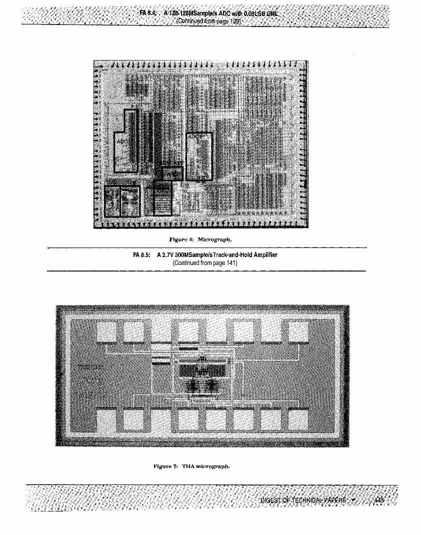
FA 8.4: A 12b 128MSamplds ADC with 0.05LSB DNL (Continued from page 139)
Figure 4: Micrograph.
FA 8.5: A 2.7V 300MSamplelsTrack-and-Hold Amplifier (Continued from page 141)
Figure 7: THA micrograph.
DIGEST OF TECHNICAL PAPERS 443 . _ _


![Parallel Computingparallelcomp.github.io/Lecture2.pdf · 1 0 ( [ ]) n i f A i A: fA: f sum A = array of all data fA = f(A) s = sum(fA) s: Programming Model 1: Shared Memory • Program](https://img.pdfslide.us/doc/110x75/5f4a23a4c6d65051555d0ce3/parallel-c-1-0-n-i-f-a-i-a-fa-f-sum-a-array-of-all-data-fa-fa-s-.jpg)