Embed Size (px)
Citation preview
DC-DC Converters for PV
ApplicationsPart I: the Active-Passive
Bridge Converter
Giorgio Spiazzi
University of Padova - DEI
G. Spiazzi - University of Padova - DEI 2/29
Outline
� Introduction
� Analysis of the Active-Passive Bridge (APB) converter
� Steady-state waveforms
� Soft-switching conditions
� Voltage conversion ratio
� Design procedure
� Design example
G. Spiazzi - University of Padova - DEI 3/29
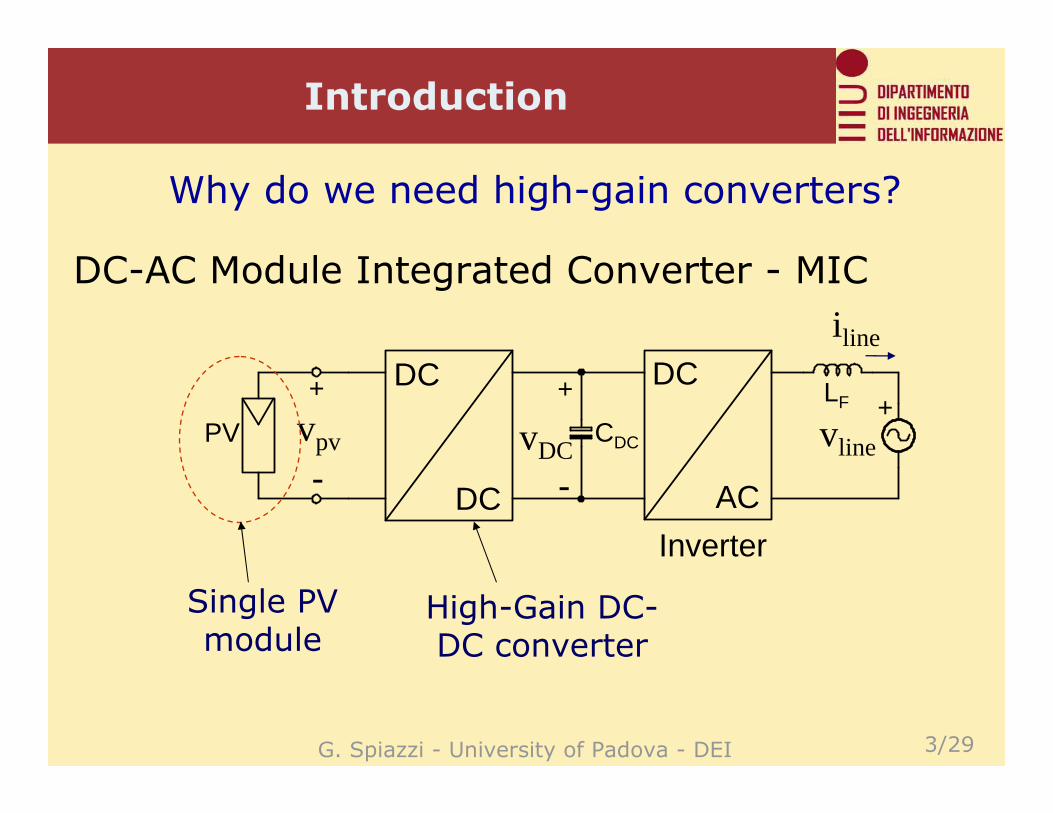
Introduction
DC
DC
DC
AC
Inverter
CDCvpv
-
+
vDC
-
+ LF +vline
i line
PV
Single PV module
High-Gain DC-DC converter
DC-AC Module Integrated Converter - MIC
Why do we need high-gain converters?
G. Spiazzi - University of Padova - DEI 4/29
Introduction
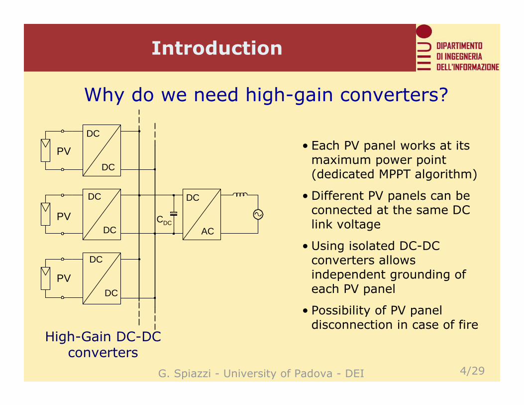
Why do we need high-gain converters?
• Each PV panel works at its maximum power point (dedicated MPPT algorithm)
• Different PV panels can be connected at the same DC link voltage
• Using isolated DC-DC converters allows independent grounding of each PV panel
• Possibility of PV panel disconnection in case of fire
DC
DC
DC
DC
DC
DC
DC
AC
PV
PV
PV
CDC
High-Gain DC-DC converters
G. Spiazzi - University of Padova - DEI 5/29
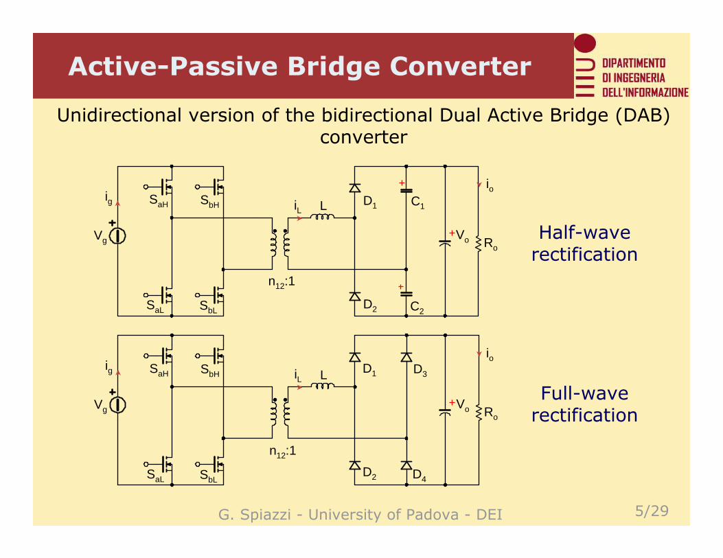
Active-Passive Bridge Converter
VoVg
io
n12:1
SaL SbL
Lig SaH SbH iL
Ro
D2 C2
D1 C1
VoVg
io
SaL SbL
Lig SaH SbH iL
Ro
D2 D4
D1 D3
n12:1
Half-wave rectification
Full-wave rectification
Unidirectional version of the bidirectional Dual Active Bridge (DAB) converter
G. Spiazzi - University of Padova - DEI 6/29
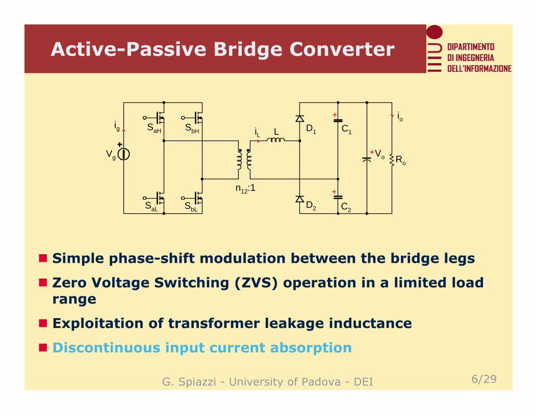
Active-Passive Bridge Converter
� Simple phase-shift modulation between the bridge legs
� Zero Voltage Switching (ZVS) operation in a limited load range
� Exploitation of transformer leakage inductance
� Discontinuous input current absorption
VoVg
io
n12:1
SaL SbL
Lig SaH SbH iL
Ro
D2 C2
D1 C1

G. Spiazzi - University of Padova - DEI 7/29
Steady-State Analysis
LiL
vA vB
� Base voltage: VN = VB
� Base impedance: ZN = ωωωωswL
� Base current: IN = VN/ZN
� Base power: PN = VN2/ ZN
Base variables:
Simplified model:
1VV
VV
kN
A
B
A >==Adimensional parameter:

G. Spiazzi - University of Padova - DEI 8/29
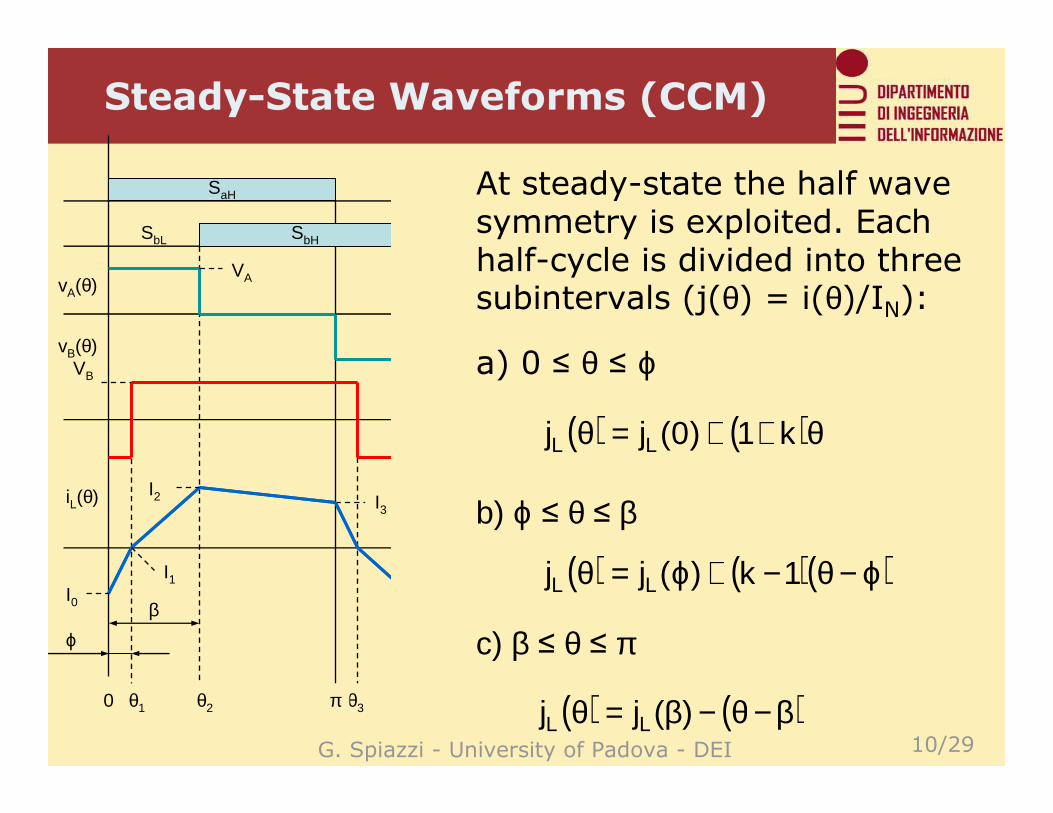
Steady-State Waveforms (CCM)
βϕ
VA
VB
I1
I2
θ1 θ2 θ30 π
I3 = -I0
I0
θ4
θ
θ
θ
θ
θ
2π
vA(θ)
vB(θ)
iL(θ)
SaH
SbHSbL SbL
SaLPhase-shift modulation of bridge legs
Three-level voltage vA
Two-level voltage vBin phase with inductor current
Piecewise linear inductor current (CCM operation)
G. Spiazzi - University of Padova - DEI 9/29
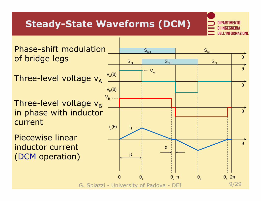
Steady-State Waveforms (DCM)
βα
VA
VB
I1
θ1 θ2 θ30 π θ4
θ
θ
θ
θ
θ
2π
vA(θ)
vB(θ)
iL(θ)
SaH
SbHSbL SbL
SaLPhase-shift modulation of bridge legs
Three-level voltage vA
Three-level voltage vBin phase with inductor current
Piecewise linearinductor current (DCM operation)
G. Spiazzi - University of Padova - DEI 10/29
Steady-State Waveforms (CCM)
βϕ
VA
VB
I1
I2
θ1 θ2 θ30 π
I3
I0
vA(θ)
vB(θ)
iL(θ)
SaH
SbHSbL
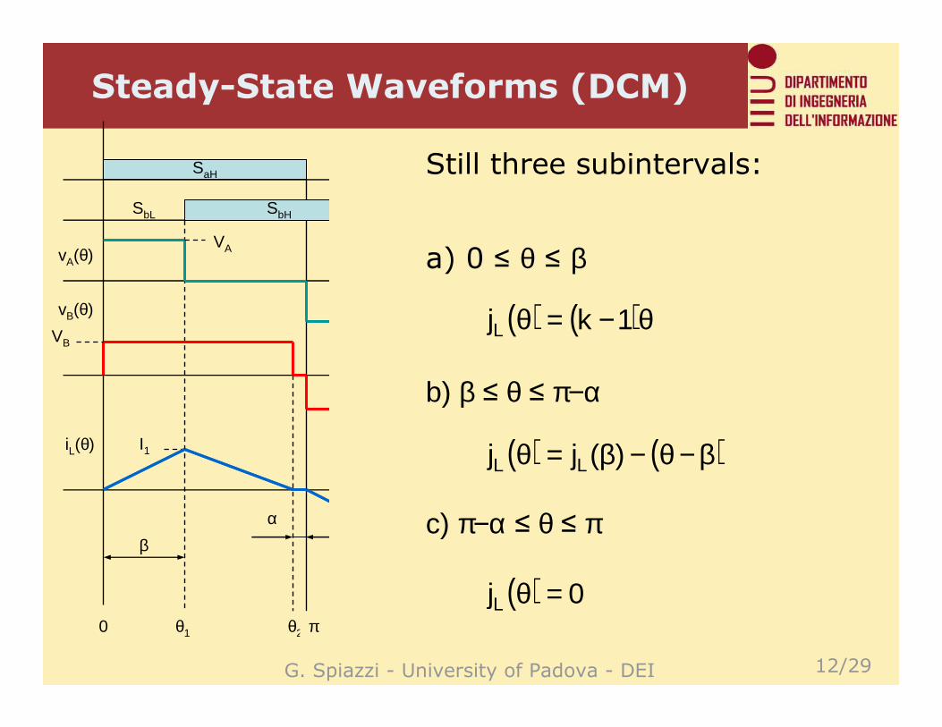
At steady-state the half wave symmetry is exploited. Each half-cycle is divided into three subintervals (j(θ) = i(θ)/IN):
a) 0 ≤ θ ≤ ϕ
b) ϕ ≤ θ ≤ β
( ) ( )θ++=θ k1)0(jj LL
c) β ≤ θ ≤ π
( ) ( )( )ϕ−θ−+ϕ=θ 1k)(jj LL
( ) ( )β−θ−β=θ )(jj LL
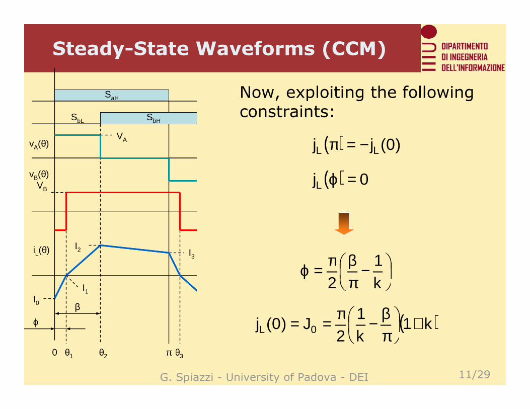
G. Spiazzi - University of Padova - DEI 11/29
Steady-State Waveforms (CCM)
βϕ
VA
VB
I1
I2
θ1 θ2 θ30 π
I3
I0
vA(θ)
vB(θ)
iL(θ)
SaH
SbHSbL
Now, exploiting the following constraints:
( ) )0(jj LL −=π
( ) 0jL =ϕ
−πβπ=ϕ
k1
2
( )k1k1
2J)0(j 0L +
πβ−π==
G. Spiazzi - University of Padova - DEI 12/29
Steady-State Waveforms (DCM)
Still three subintervals:
a) 0 ≤ θ ≤ β
b) β ≤ θ ≤ π−α
c) π−α ≤ θ ≤ π
( ) ( )β−θ−β=θ )(jj LL
βα
VA
VB
I1
θ1 θ20 π
vA(θ)
vB(θ)
iL(θ)
SaH
SbHSbL
( ) ( )θ−=θ 1kjL
( ) 0jL =θ
G. Spiazzi - University of Padova - DEI 13/29
Steady-State Waveforms (DCM)
βα
VA
VB
I1
θ1 θ20 π
vA(θ)
vB(θ)
iL(θ)
SaH
SbHSbL
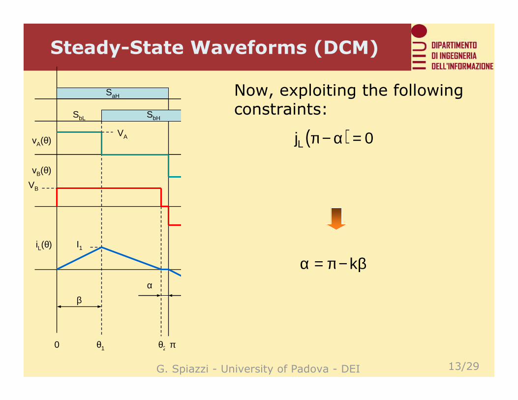
Now, exploiting the following constraints:
( ) 0jL =α−π
β−π=α k
G. Spiazzi - University of Padova - DEI 14/29
Boundary Condition
βϕ
VA
VB
I1
I2
θ1 θ2 θ30 π
I3
I0
vA(θ)
vB(θ)
iL(θ)
SaH
SbHSbL
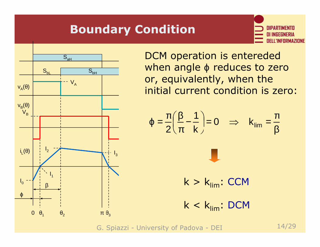
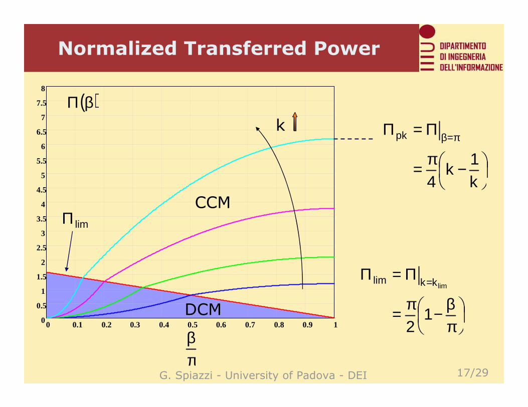
DCM operation is enterededwhen angle ϕ reduces to zero or, equivalently, when the initial current condition is zero:
βπ=⇒=
−πβπ=ϕ limk0
k1
2
k > klim: CCM
k < klim: DCM
G. Spiazzi - University of Padova - DEI 15/29
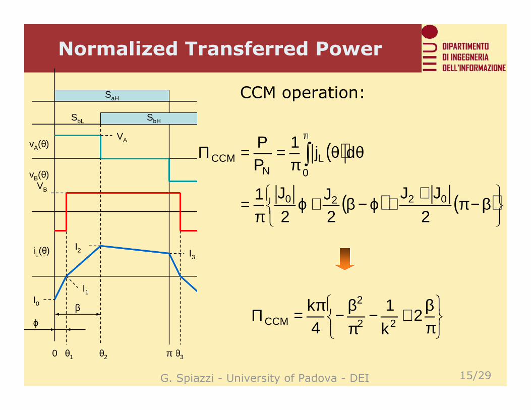
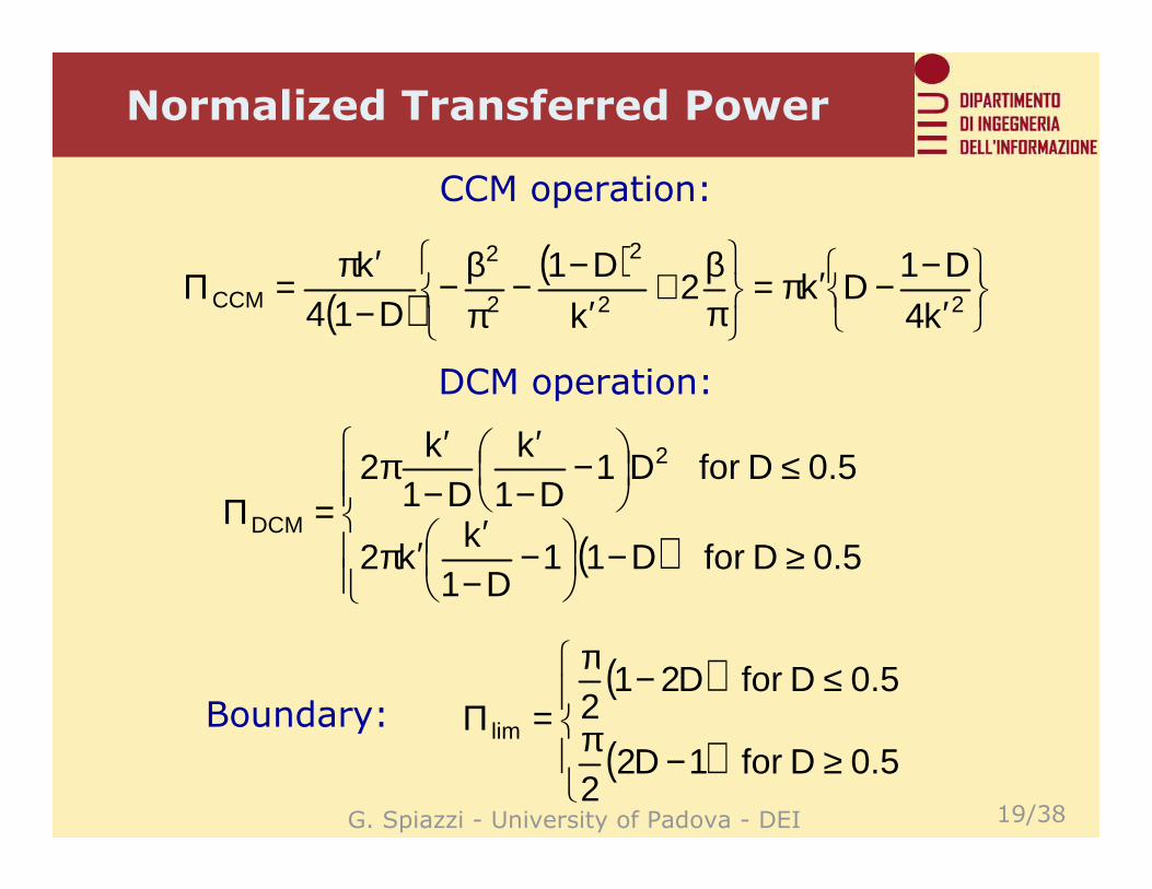
Normalized Transferred Power
( )
( ) ( )
β−π
++ϕ−β+ϕ
π=
θθπ
==Π ∫π
2
JJ
2J
2
J1
dj1
PP
0220
0L
NCCM
βϕ
VA
VB
I1
I2
θ1 θ2 θ30 π
I3
I0
vA(θ)
vB(θ)
iL(θ)
SaH
SbHSbL
πβ+−
πβ−π=Π 2
k
14k
22
2
CCM
CCM operation:
G. Spiazzi - University of Padova - DEI 16/29
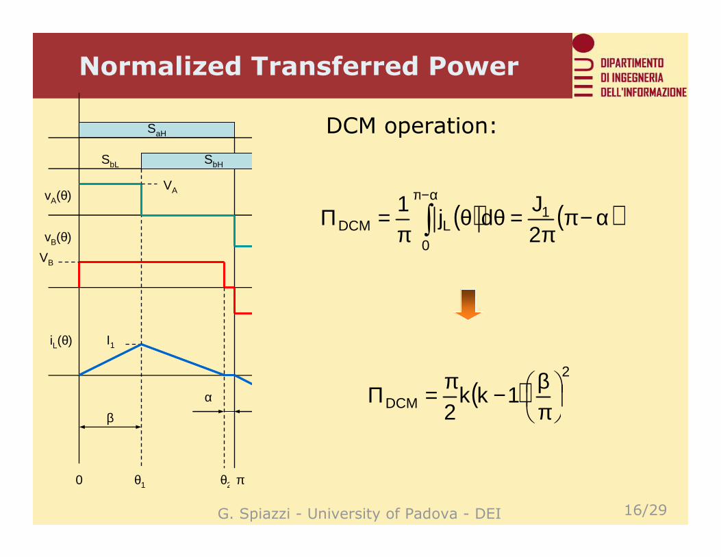
Normalized Transferred Power
DCM operation:
βα
VA
VB
I1
θ1 θ20 π
vA(θ)
vB(θ)
iL(θ)
SaH
SbHSbL
( ) ( )α−ππ
=θθπ
=Π ∫α−π
2J
dj1 1
0LDCM
( )2
DCM 1kk2
πβ−π=Π
G. Spiazzi - University of Padova - DEI 17/29
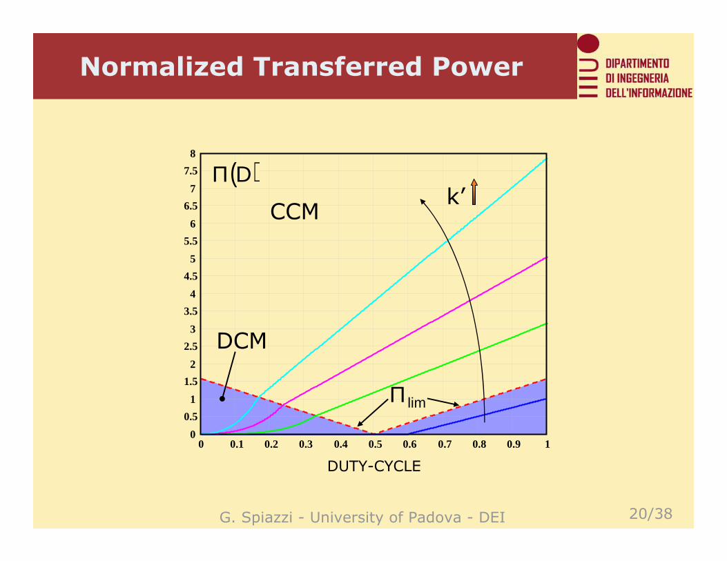
Normalized Transferred Power
0 0.1 0.2 0.3 0.4 0.5 0.6 0.7 0.8 0.9 10
0.5
1
1.5
2
2.5
3
3.5
4
4.5
5
5.5
6
6.5
7
7.5
8
k
πβ
( )βΠ
DCM
CCM
πβ−π=
Π=Π =
12
limkklim
limΠ
−π=
Π=Π π=β
k1
k4
pk
G. Spiazzi - University of Padova - DEI 18/29
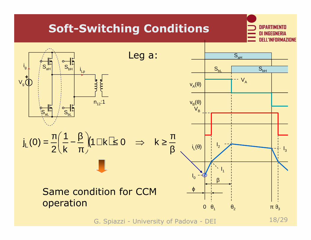
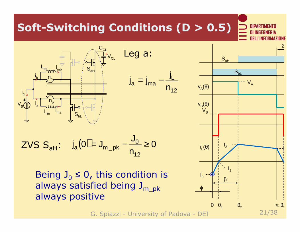
Soft-Switching Conditions
Vg
n12:1
SaL SbL
ig SaH SbH iLp
βϕ
VA
VB
I1
I2
θ1 θ2 θ30 π
I3
I0
vA(θ)
vB(θ)
iL(θ)
SaH
SbHSbL
Leg a:
( )βπ≥⇒≤+
πβ−π= k0k1
k1
2)0(jL
Same condition for CCM operation
G. Spiazzi - University of Padova - DEI 19/29
Soft-Switching Conditions
Vg
n12:1
SaL SbL
ig SaH SbH iLp
βϕ
VA
VB
I1
I2
θ1 θ2 θ30 π
I3
I0
vA(θ)
vB(θ)
iL(θ)
SaH
SbHSbL
Leg b:
Always verified
1k0k2
1kJ2 ≥⇒≥
β+π
−=
G. Spiazzi - University of Padova - DEI 20/29
Voltage Conversion Ratio
FnM
kFn1
VV
M1212g
o ′===
=
rectifier wave-half 5.0
rectifier wave-full 1F
VoVg
io
n12:1
SaL SbL
Lig SaH SbH iL
Ro
D2 C2
D1 C1
Definition:
k1
M =′
where:
oB FVV =
12
gA n
VV =
G. Spiazzi - University of Padova - DEI 21/29
Voltage Conversion Ratio
VoVg
io
n12:1
SaL SbL
Lig SaH SbH iL
Ro
D2 C2
D1 C1
o2
o2
L2B
L
o
2o
N
o
F
1
RF
X
V
XRV
PP
ρ====ΠConsidering a resistive load:
L
oo X
R=ρNormalized load resistance:
oB FVV =
G. Spiazzi - University of Padova - DEI 22/29
Voltage Conversion Ratio
o2CCM
F
1
ρ=Π
ρπ
πβ−β++−
ρπ=′
4F
211F
2M
2o
4
o2CCM
o2DCM
F
1
ρ=Π
ρβπ+−
πβρ−=′
o22
2o
2
DCMF
811
4F
M
Boundary condition:o
2limF
21M
ρπ−=′
ZVS is ensured for any βvalue only if: 2olim
F
20M
π≤ρ⇒≤′
G. Spiazzi - University of Padova - DEI 23/29
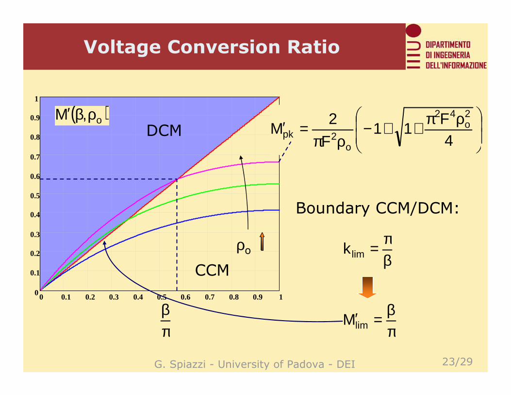
Voltage Conversion Ratio
0 0.1 0.2 0.3 0.4 0.5 0.6 0.7 0.8 0.9 10
0.1
0.2
0.3
0.4
0.5
0.6
0.7
0.8
0.9
1
πβ
( )o,M ρβ′
ρo
DCM
CCM
ρπ++−ρπ
=′4
F11
F
2M
2o
42
o2pk
βπ=limk
Boundary CCM/DCM:
πβ=′limM
G. Spiazzi - University of Padova - DEI 24/29
Design Parameters
� Minimum input voltage: Vg_min = 25 V
� Maximum input voltage: Vg_max = 35 V
� Nominal output voltage: Vo = 400 V
� Nominal output power: Po = 300 W
� Minimum output power for CCM: Po_min = 200 W
� Switching frequency: fsw = 100 kHz
� Rectifier type: F = 0.5
� Maximum phase-shift angle: ββββmax = 0.8 ππππ
Goal: determine transformer turns ratio n12and current shaping inductor L
G. Spiazzi - University of Padova - DEI 25/29
Design Procedure
1. Maximum voltage conversion ratio is reached at nominal power and maximum phase-shift angle ββββmax
( ) 02MFnRF
X4MFn max
2max
max12min_o
2L2
max12 =π
β−
πβ+
π+
max_o2
Lmin12
RF
X21MFn
π−=
2. Minimum voltage conversion ratio is reached at minimum power (corresponding to CCM-DCM boundary condition)
G. Spiazzi - University of Padova - DEI 26/29
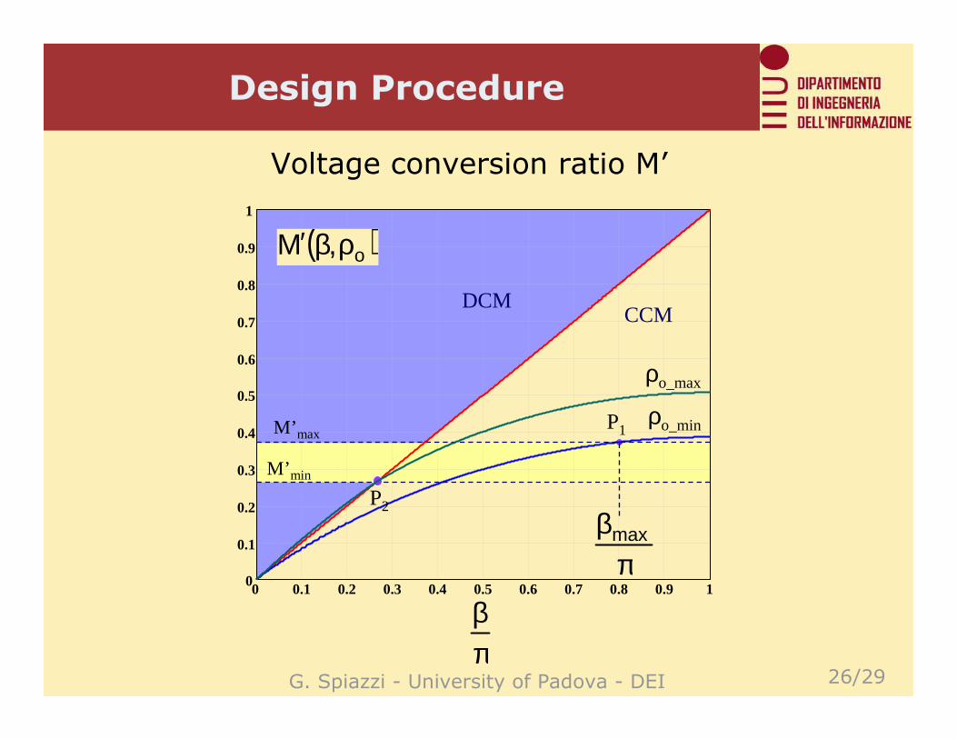
Design Procedure
0 0.1 0.2 0.3 0.4 0.5 0.6 0.7 0.8 0.9 10
0.1
0.2
0.3
0.4
0.5
0.6
0.7
0.8
0.9
1
M’ max
M’ min
ρo_max
ρo_minP1
P2
CCM
πβ
πβmax
( )o,M ρβ′
DCM
Voltage conversion ratio M’
G. Spiazzi - University of Padova - DEI 27/29
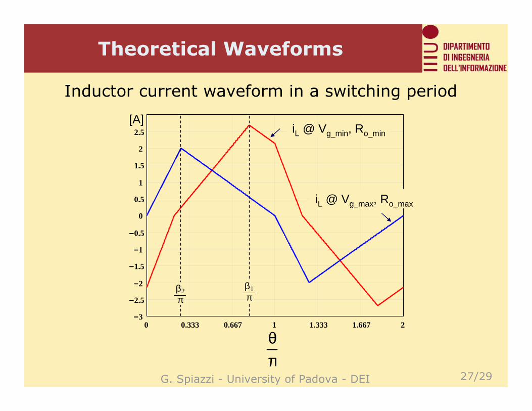
Theoretical Waveforms
0 0.333 0.667 1 1.333 1.667 23−−−−
2.5−−−−
2−−−−
1.5−−−−
1−−−−
0.5−−−−
0
0.5
1
1.5
2
2.5[A]
β2
πβ1
π
iL @ Vg_min, Ro_min
iL @ Vg_max, Ro_max
πθ
Inductor current waveform in a switching period
G. Spiazzi - University of Padova - DEI 28/29
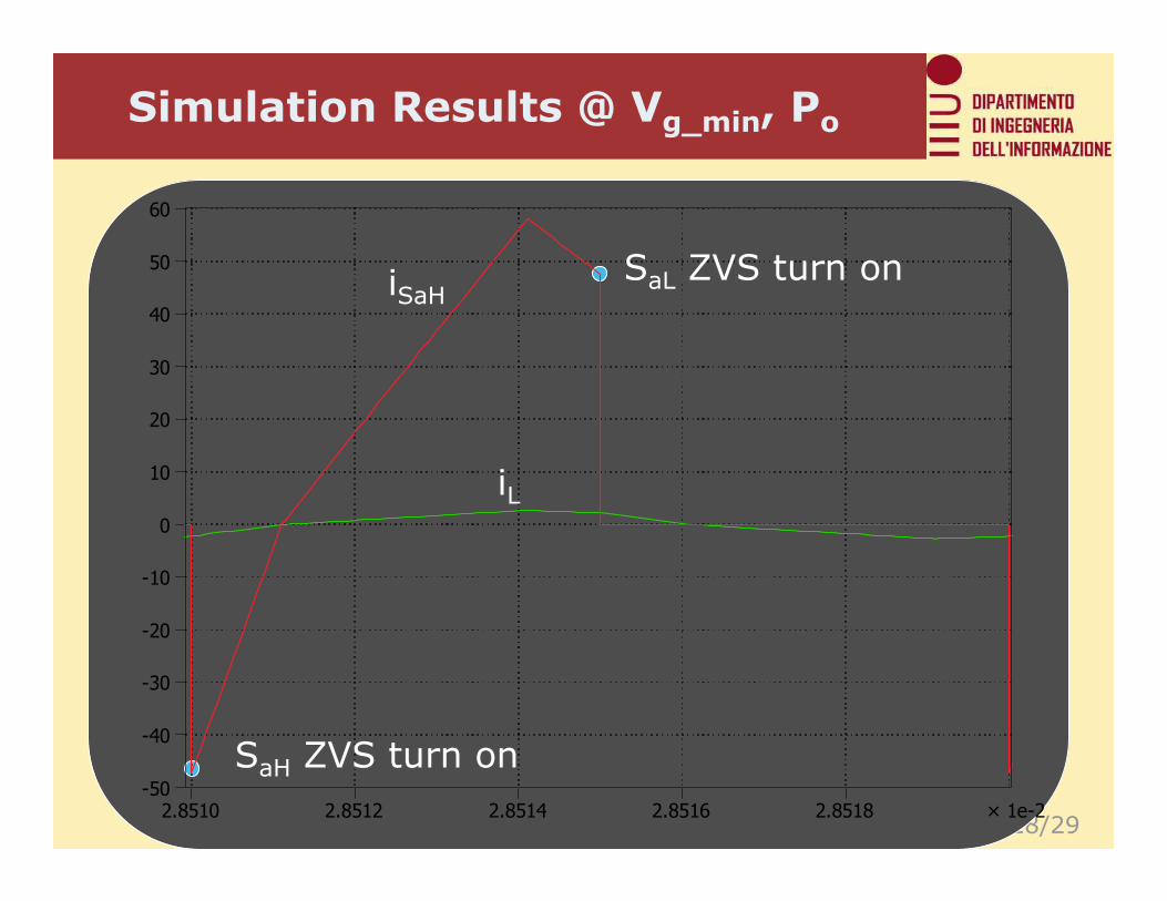
Simulation Results @ Vg_min, Po
× 1e-22.8510 2.8512 2.8514 2.8516 2.8518
-50
-40
-30
-20
-10
0
10
20
30
40
50
60
iL
iSaH
SaH ZVS turn on
SaL ZVS turn on
G. Spiazzi - University of Padova - DEI 29/29
Conclusions
� The Active-Passive Bridge converter operation was analyzed in normalized form
� The voltage conversion ratio was derived for both CCM and DCM operation
� A design procedure has been developed and verified by simulation
DC-DC Converters for PV
ApplicationsPart II: the Interleaved Boost
with Coupled Inductors
Giorgio Spiazzi
University of Padova - DEI
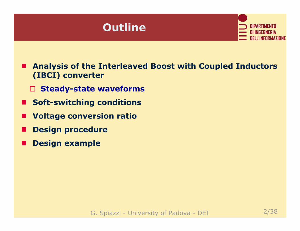
G. Spiazzi - University of Padova - DEI 2/38
Outline
� Analysis of the Interleaved Boost with Coupled Inductors (IBCI) converter
� Steady-state waveforms
� Soft-switching conditions
� Voltage conversion ratio
� Design procedure
� Design example
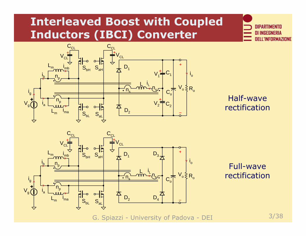
G. Spiazzi - University of Padova - DEI 3/38
Interleaved Boost with Coupled Inductors (IBCI) Converter
Half-wave rectification
Full-wave rectification
V2
V1
D1
L
SbL
Vo
C2
C1
SaL
Vg
iL
ia
io
D2
np
npib
SbH SaHLm imb
Lmima
nsnsig
VCL
CCL CCL
VCL
RoCo
D4
D3D1
L
SbL
Vo
SaL
Vg
iL
ia
io
D2
np
npib
SbH SaHLm imb
Lmima
nsnsig
VCL
CCL CCL
VCL
RoCo
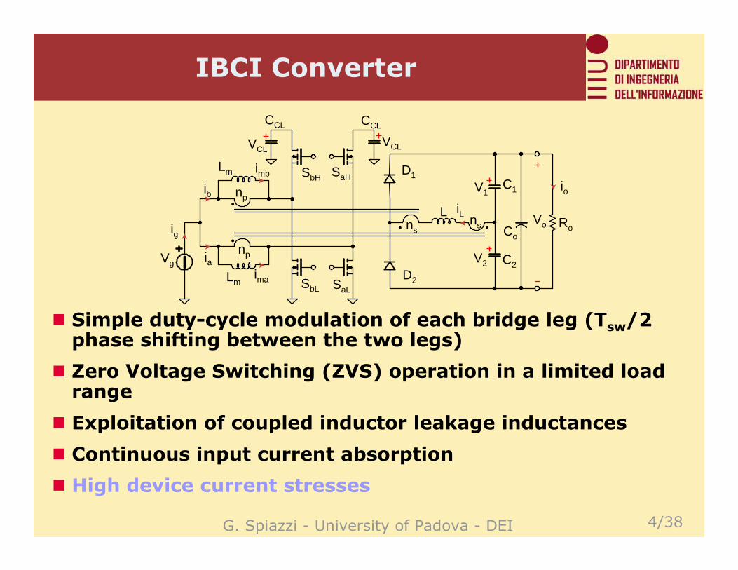
G. Spiazzi - University of Padova - DEI 4/38
IBCI Converter
� Simple duty-cycle modulation of each bridge leg (Tsw/2 phase shifting between the two legs)
� Zero Voltage Switching (ZVS) operation in a limited load range
� Exploitation of coupled inductor leakage inductances
� Continuous input current absorption
� High device current stresses
V2
V1
D1
L
SbL
Vo
C2
C1
SaL
Vg
iL
ia
io
D2
np
npib
SbH SaHLm imb
Lmima
nsnsig
VCL
CCL CCL
VCL
RoCo
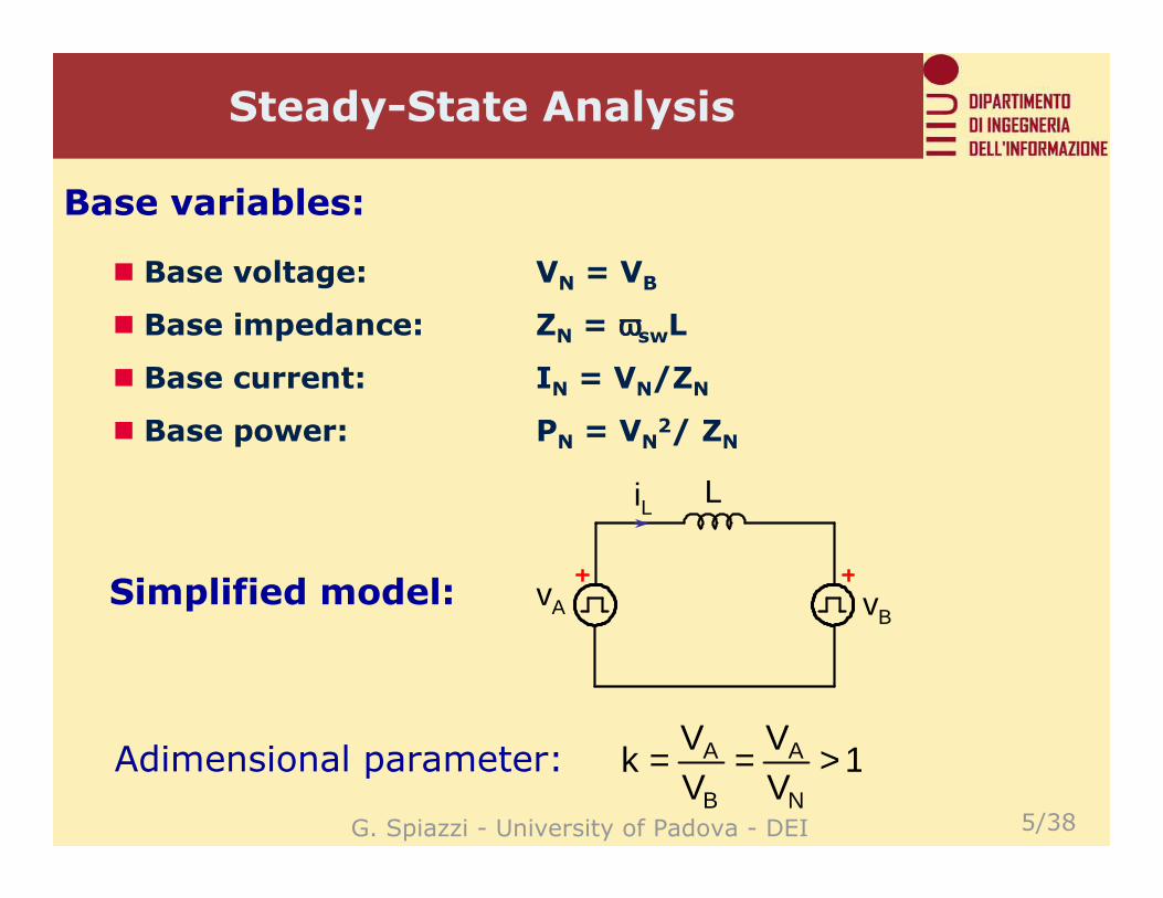
G. Spiazzi - University of Padova - DEI 5/38
Steady-State Analysis
LiL
vA vB
� Base voltage: VN = VB
� Base impedance: ZN = ωωωωswL
� Base current: IN = VN/ZN
� Base power: PN = VN2/ ZN
Base variables:
Simplified model:
1VV
VV
kN
A
B
A >==Adimensional parameter:
G. Spiazzi - University of Padova - DEI 6/38
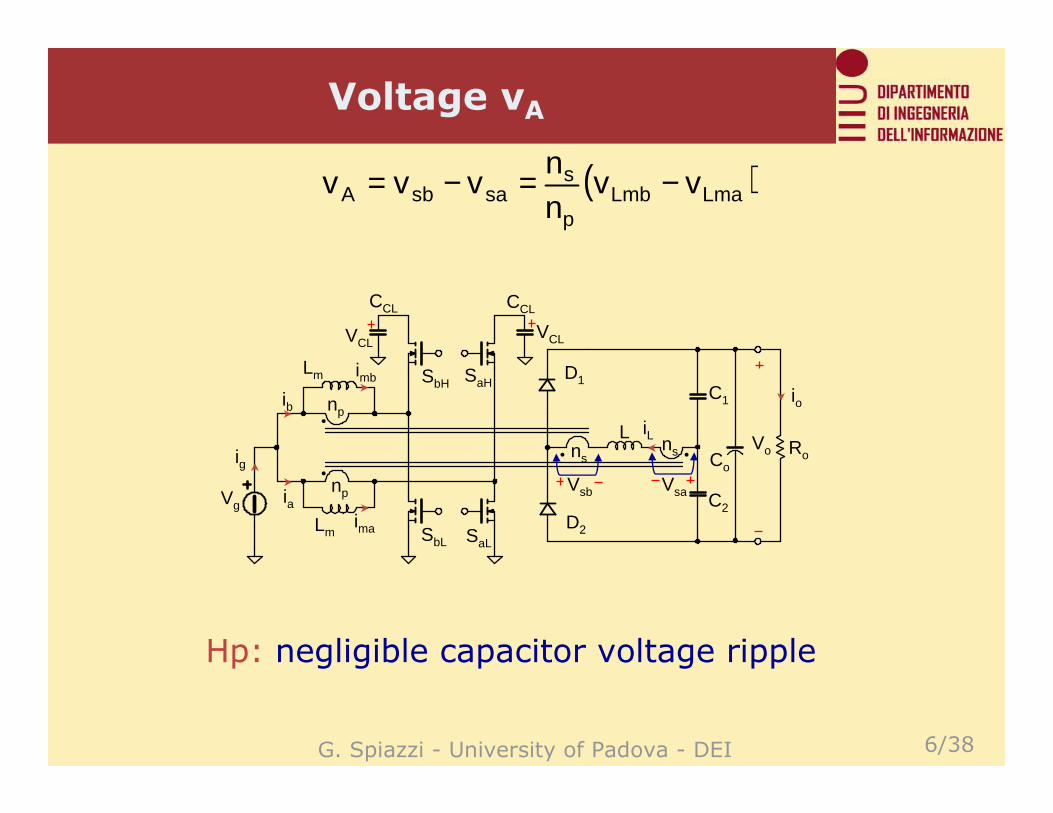
Voltage vA
( )LmaLmbp
ssasbA vv
nn
vvv −=−=
Vsb Vsa
D1
L
SbL
Vo
C2
C1
SaL
Vg
iL
ia
io
D2
np
npib
SbH SaHLm imb
Lmima
nsnsig
VCL
CCL CCL
VCL
RoCo
Hp: negligible capacitor voltage ripple
G. Spiazzi - University of Padova - DEI 7/38
Voltage vA
Vg ianp
npib
SbH SaHLm imb
Lmima
ig
VCL
CCL CCL
VCL
SbL SaL
Vg ianp
npib
Lm imb
Lmima
ig
( )LmaLmbp
ssasbA vv
nn
vvv −=−=
( )0
VVVVnn
v CLgCLgp
sA
=
+−−= ( )0
VVnn
v ggp
sA
=
−=
Upper switches “on” Lower switches “on”
G. Spiazzi - University of Padova - DEI 8/38
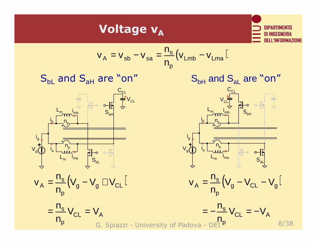
Voltage vA
( )LmaLmbp
ssasbA vv
nn
vvv −=−=
( )
ACLp
s
CLggp
sA
VVnn
VVVnn
v
==
+−= ( )
ACLp
s
gCLgp
sA
VVnn
VVVnn
v
−=−=
−−=
SbL and SaH are “on” SbH and SaL are “on”
SbL
Vg ianp
npib
SaHLm imb
Lmima
ig
CCL
VCL
SaL
Vg ianp
npib
SbHLm imb
Lmima
ig
VCL
CCL
G. Spiazzi - University of Padova - DEI 9/38
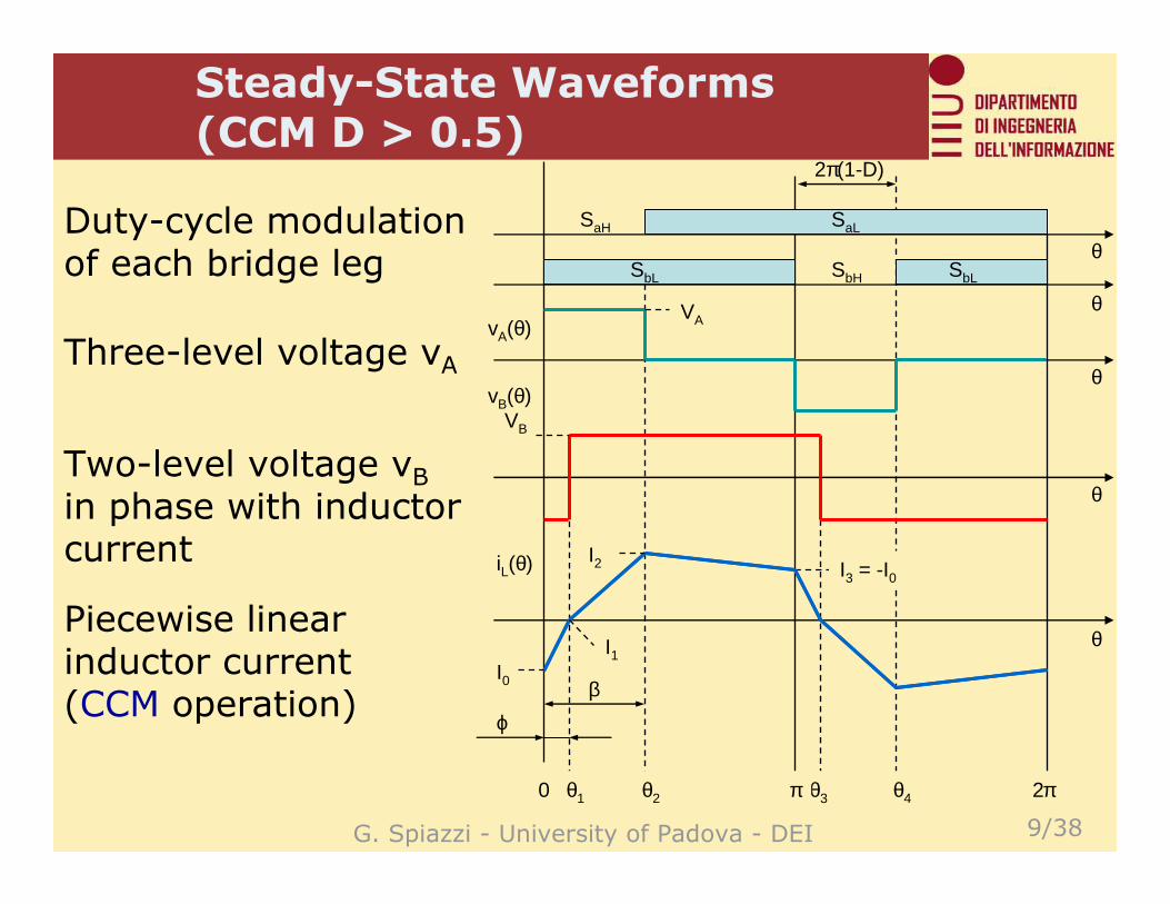
Steady-State Waveforms(CCM D > 0.5)
Duty-cycle modulation of each bridge leg
Three-level voltage vA
Two-level voltage vBin phase with inductor current
Piecewise linear inductor current (CCM operation)
βϕ
VA
VB
I1
I2
θ1 θ2 θ30 π
I3 = -I0
I0
θ4
θ
θ
θ
θ
θ
2π
vA(θ)
vB(θ)
iL(θ)
SaH
SbHSbL
SaL
2π(1-D)
SbL
G. Spiazzi - University of Padova - DEI 10/38
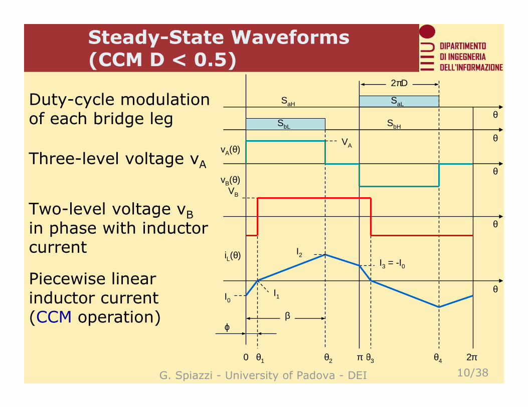
Steady-State Waveforms(CCM D < 0.5)
Duty-cycle modulation of each bridge leg
Three-level voltage vA
Two-level voltage vBin phase with inductor current
Piecewise linear inductor current (CCM operation)
ϕ
VA
VB
I1
I2
θ1 θ2 θ30 π
I3 = -I0
I0
θ4
θ
θ
θ
θ
θ
2π
vA(θ)
vB(θ)
iL(θ)
SaH
SbHSbL
SaL
2πD
β
G. Spiazzi - University of Padova - DEI 11/38
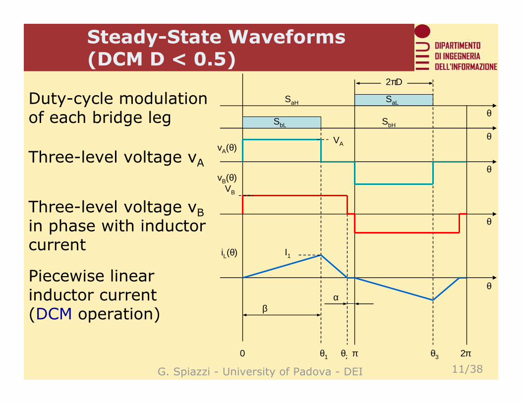
Steady-State Waveforms(DCM D < 0.5)
Three-level voltage vA
Three-level voltage vBin phase with inductor current
Piecewise linearinductor current (DCM operation)
Duty-cycle modulation of each bridge leg
βα
VA
VB
I1
θ1 θ2 θ30 π
θ
θ
θ
θ
θ
2π
vA(θ)
vB(θ)
iL(θ)
SaH
SbHSbL
SaL
2πD
G. Spiazzi - University of Padova - DEI 12/38
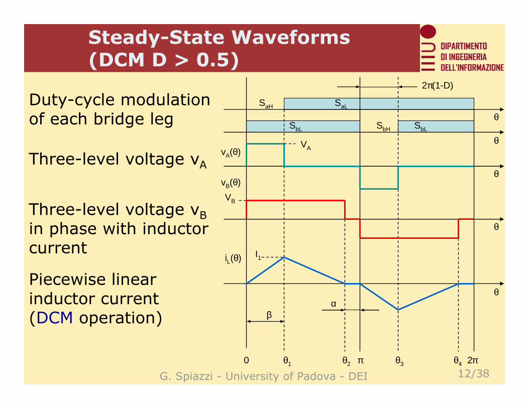
Steady-State Waveforms(DCM D > 0.5)
βα
VA
VB
I1
θ1 θ2 θ30 π
θ
θ
θ
θ
θ
2π
vA(θ)
vB(θ)
iL(θ)
SaH
SbHSbL
SaL
2π(1-D)
SbL
θ4
Three-level voltage vA
Three-level voltage vBin phase with inductor current
Piecewise linearinductor current (DCM operation)
Duty-cycle modulation of each bridge leg
G. Spiazzi - University of Padova - DEI 13/38
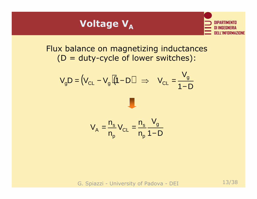
Voltage VA
( )( )D1
VVD1VVDV g
CLgCLg −=⇒−−=
Flux balance on magnetizing inductances (D = duty-cycle of lower switches):
D1
V
nn
Vnn
V g
p
sCL
p
sA −
==
G. Spiazzi - University of Padova - DEI 14/38
Steady-State Behavior
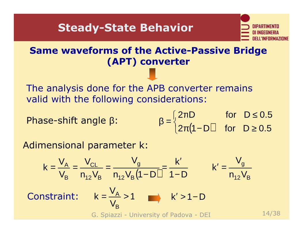
Same waveforms of the Active-Passive Bridge (APT) converter
( )
≥−π≤π
=β5.0D orf D12
5.0D orf D2Phase-shift angle β:
( ) D1k
D1Vn
V
VnV
VV
kB12
g
B12
CL
B
A
−′
=−
===B12
g
Vn
Vk =′
Adimensional parameter k:
The analysis done for the APB converter remains valid with the following considerations:
1VV
kB
A >= D1k −>′Constraint:
G. Spiazzi - University of Padova - DEI 15/38
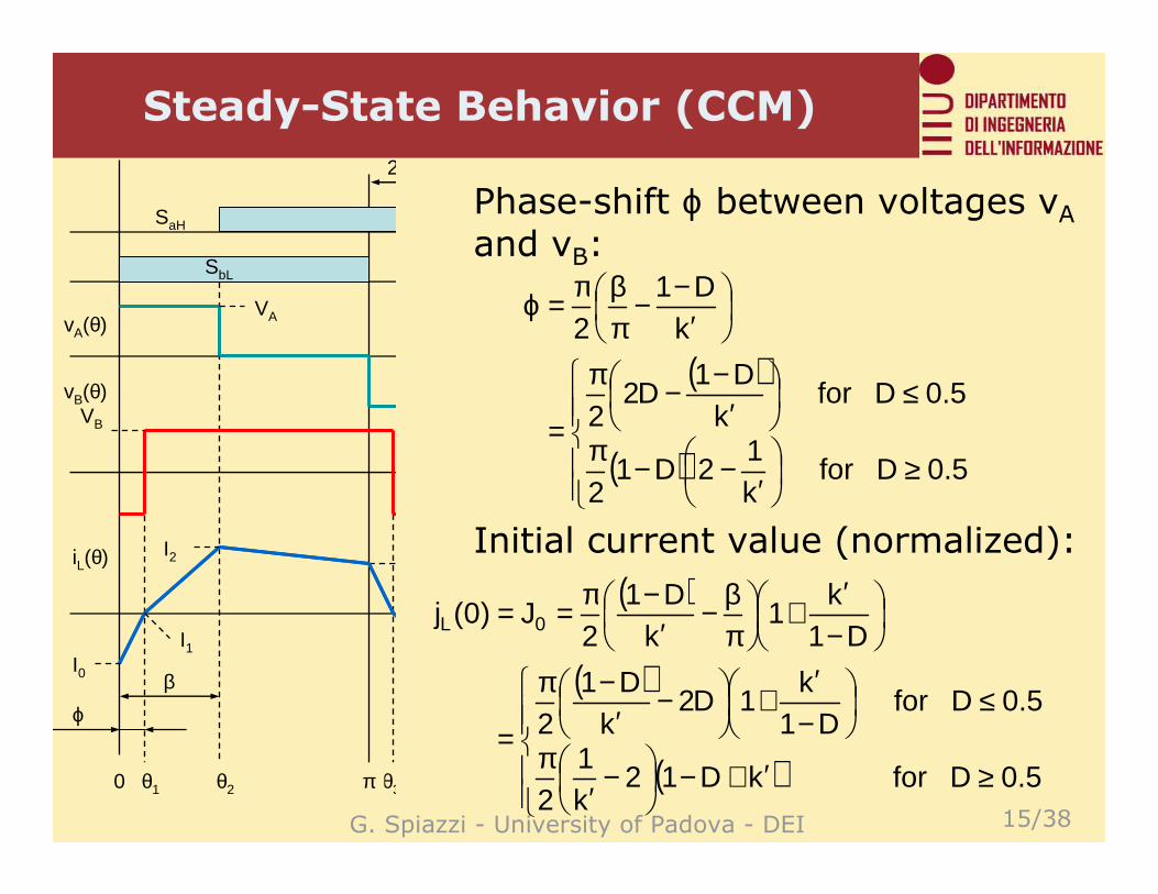
Steady-State Behavior (CCM)
Phase-shift ϕ between voltages vAand vB:
( )
( )
≥
′−−π
≤
′−−π
=
′−−
πβπ=ϕ
0.5D for k1
2D12
0.5D for k
D1D2
2
kD1
2
Initial current value (normalized):
( )
( )
( )
≥′+−
−′
π
≤
−′
+
−′
−π
=
−′
+
πβ−
′−π==
0.5D for kD12k1
2
0.5D for D1
k1D2
kD1
2
D1k
1k
D12
J)0(j 0L
βϕ
VA
VB
I1
I2
θ1 θ2 θ30 π
I0
vA(θ)
vB(θ)
iL(θ)
SaH
SbL
2
G. Spiazzi - University of Padova - DEI 16/38
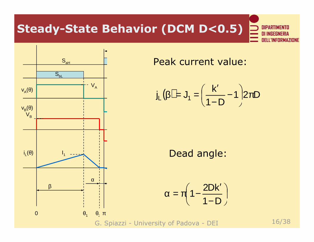
Steady-State Behavior (DCM D<0.5)
Peak current value:
Dead angle:
( ) D21D1
kJj 1L π
−−
′==β
βα
VA
VB
I1
θ1 θ20 π
vA(θ)
vB(θ)
iL(θ)
SaH
SbL
−′
−π=αD1kD2
1
G. Spiazzi - University of Padova - DEI 17/38
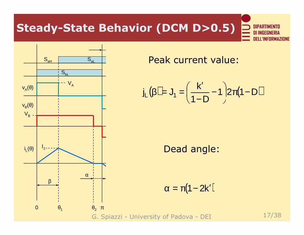
Steady-State Behavior (DCM D>0.5)
Peak current value:
Dead angle:
( ) ( )D121D1
kJj 1L −π
−−
′==β
( )k21 ′−π=αβ
α
VA
VB
I1
θ1 θ20 π
vA(θ)
vB(θ)
iL(θ)
SaH
SbL
SaL
G. Spiazzi - University of Padova - DEI 18/38
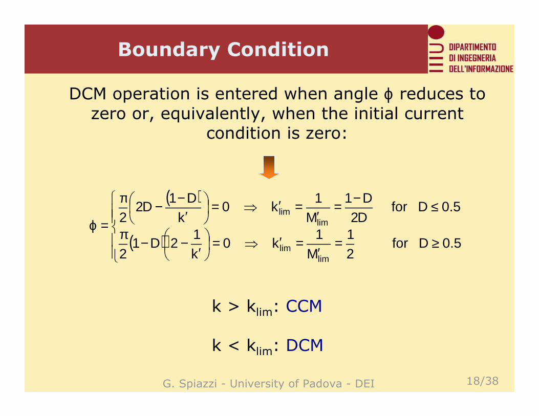
Boundary Condition
DCM operation is entered when angle ϕ reduces to zero or, equivalently, when the initial current
condition is zero:
k > klim: CCM
k < klim: DCM
( )
( )
≥=′
=′⇒=
′−−π
≤−=′
=′⇒=
′−−π
=ϕ0.5D for
21
M1
k0k1
2D12
0.5D for D2D1
M1
k0k
D1D2
2
limlim
limlim
G. Spiazzi - University of Padova - DEI 19/38
Normalized Transferred Power
CCM operation:
( )( )
′−−′π=
πβ+
′−−
πβ−
−′π=Π
22
2
2
2
CCMk4
D1Dk2
k
D1D14
k
DCM operation:
Boundary:
( )
≥−
−−
′′π
≤
−−
′−
′π
=Π0.5D for D11
D1k
k2
0.5D for D1D1
kD1
k2 2
DCM
( )
( )
≥−π
≤−π
=Π0.5D for 1D2
2
0.5D for D212
lim
G. Spiazzi - University of Padova - DEI 20/38
Normalized Transferred Power
0 0.1 0.2 0.3 0.4 0.5 0.6 0.7 0.8 0.9 10
0.5
1
1.5
2
2.5
3
3.5
4
4.5
5
5.5
6
6.5
7
7.5
8
( )DΠ
DCM
CCM
limΠ
k’
DUTY-CYCLE
G. Spiazzi - University of Padova - DEI 21/38
SbL
Vg ianp
npib
SaHLm imb
Lmima
ig
CCL
VCL
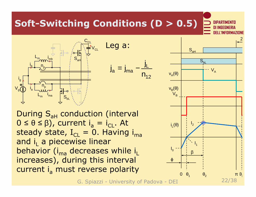
Soft-Switching Conditions (D > 0.5)
Leg a:
βϕ
VA
VB
I1
I2
θ1 θ2 θ30 π
I0
vA(θ)
vB(θ)
iL(θ)
SaH
SbL
2
12
Lmaa n
jjj −=
( ) 0nJ
J0j12
0pk_ma ≥−=ZVS SaH:
Being J0 ≤ 0, this condition is always satisfied being Jm_pkalways positive
G. Spiazzi - University of Padova - DEI 22/38
SbL
Vg ianp
npib
SaHLm imb
Lmima
ig
CCL
VCL
Soft-Switching Conditions (D > 0.5)
Leg a:
βϕ
VA
VB
I1
I2
θ1 θ2 θ30 π
I0
vA(θ)
vB(θ)
iL(θ)
SaH
SbL
2
12
Lmaa n
jjj −=
During SaH conduction (interval 0 ≤ θ ≤ β), current ia = iCL. At steady state, ICL = 0. Having imaand iL a piecewise linear behavior (ima decreases while iLincreases), during this interval current ia must reverse polarity
G. Spiazzi - University of Padova - DEI 23/38
SbL SaL
Vg ianp
npib
Lm imb
Lmima
ig
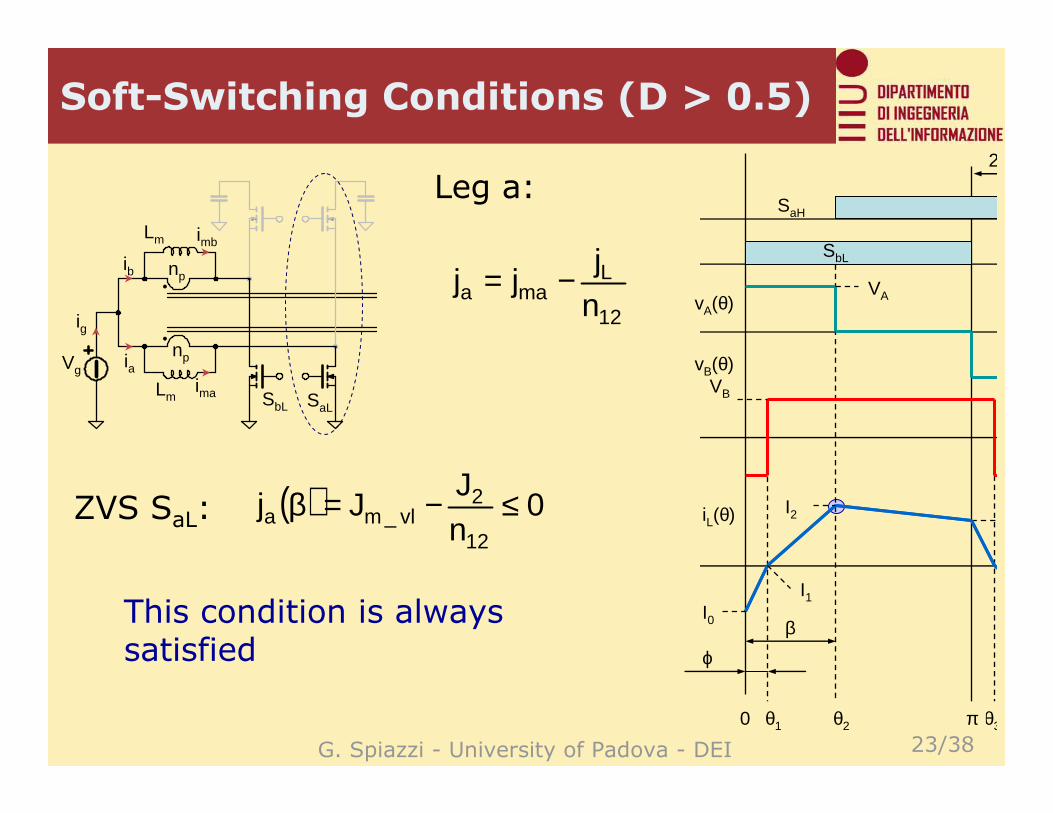
Soft-Switching Conditions (D > 0.5)
Leg a:
βϕ
VA
VB
I1
I2
θ1 θ2 θ30 π
I0
vA(θ)
vB(θ)
iL(θ)
SaH
SbL
2
12
Lmaa n
jjj −=
( ) 0nJ
Jj12
2vl_ma ≤−=βZVS SaL:
This condition is always satisfied
G. Spiazzi - University of Padova - DEI 24/38
Vg ianp
npib
SbH SaHLm imb
Lmima
ig
VCL
CCL CCL
VCL
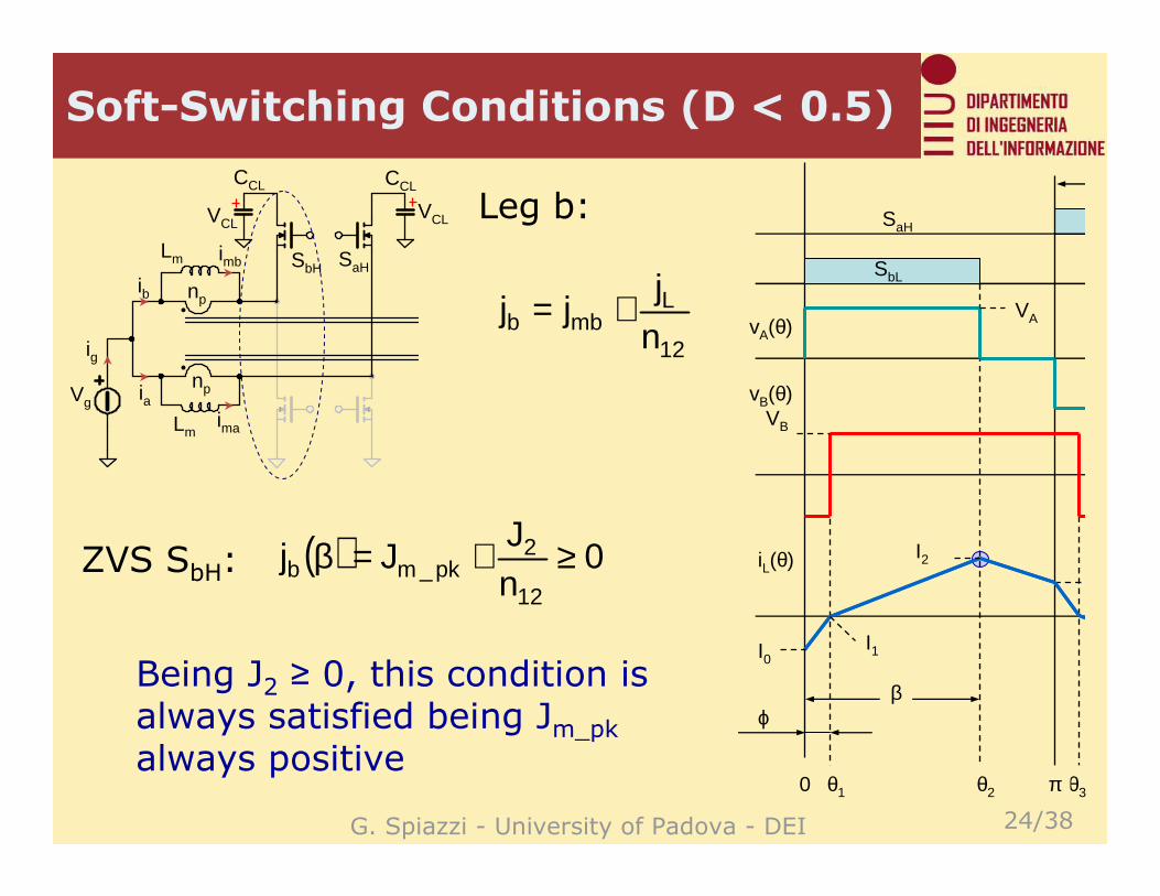
Soft-Switching Conditions (D < 0.5)
Leg b:
12
Lmbb n
jjj +=
( ) 0nJ
Jj12
2pk_mb ≥+=βZVS SbH:
Being J2 ≥ 0, this condition is always satisfied being Jm_pkalways positive
ϕ
VA
VB
I1
I2
θ1 θ2 θ30 π
I0
vA(θ)
vB(θ)
iL(θ)
SaH
SbL
β
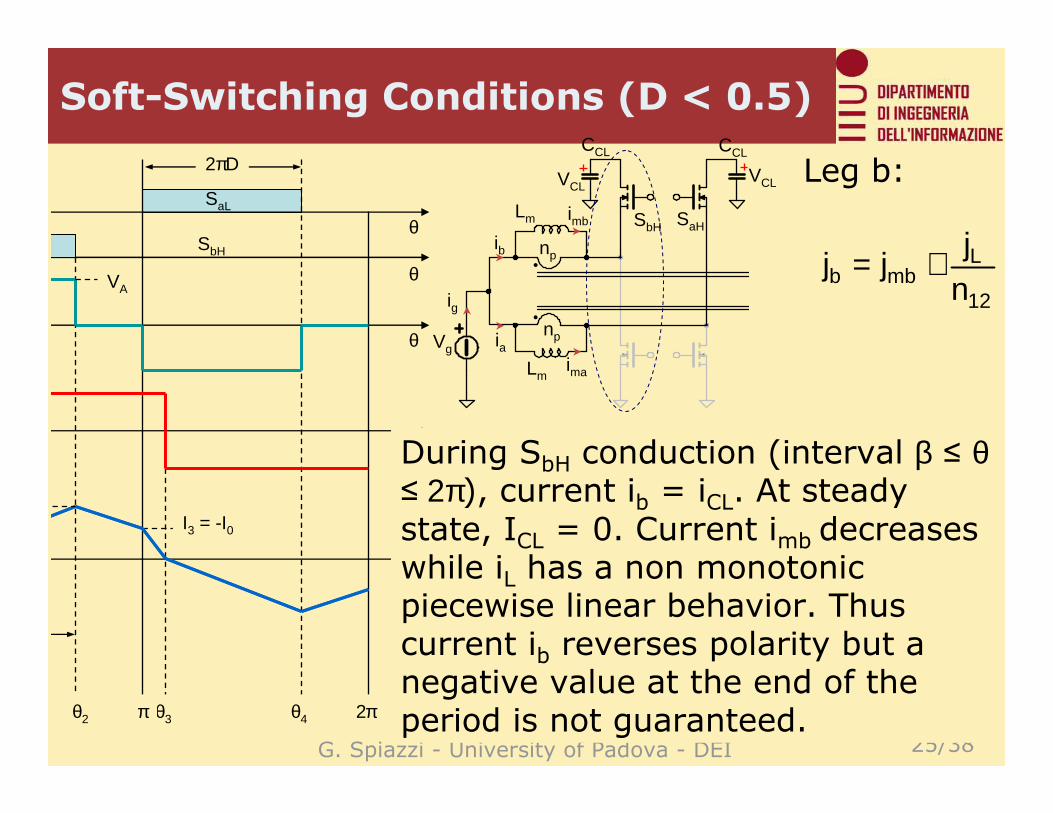
G. Spiazzi - University of Padova - DEI 25/38
Vg ianp
npib
SbH SaHLm imb
Lmima
ig
VCL
CCL CCL
VCL
Soft-Switching Conditions (D < 0.5)
Leg b:
12
Lmbb n
jjj +=
VA
θ2 θ3π
I3 = -I0
θ4
θ
θ
θ
θ
θ
2π
SbH
SaL
2πD
During SbH conduction (interval β ≤ θ≤ 2π), current ib = iCL. At steady state, ICL = 0. Current imb decreases while iL has a non monotonic piecewise linear behavior. Thus current ib reverses polarity but a negative value at the end of the period is not guaranteed.
G. Spiazzi - University of Padova - DEI 26/38
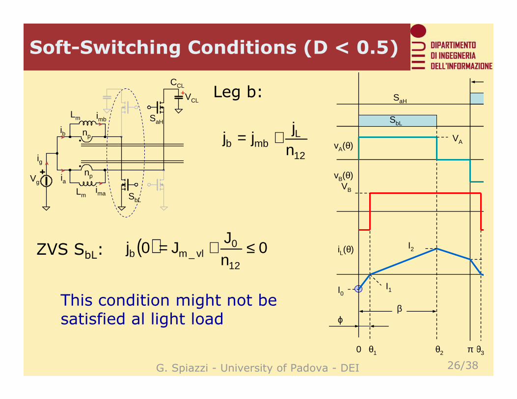
SbL
Vg ianp
npib
SaHLm imb
Lmima
ig
CCL
VCL
Soft-Switching Conditions (D < 0.5)
Leg b:
12
Lmbb n
jjj +=
( ) 0nJ
J0j12
0vl_mb ≤+=ZVS SbL:
This condition might not be satisfied al light load ϕ
VA
VB
I1
I2
θ1 θ2 θ30 π
I0
vA(θ)
vB(θ)
iL(θ)
SaH
SbL
β
G. Spiazzi - University of Padova - DEI 27/38
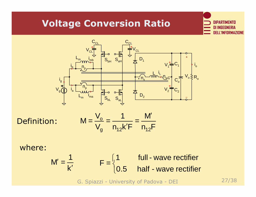
Voltage Conversion Ratio
FnM
Fkn1
VV
M1212g
o ′=
′==
=
rectifier wave-half 5.0
rectifier wave-full 1F
Definition:
k1
M′
=′
where:
V2
V1
D1
L
SbL
Vo
C2
C1
SaL
Vg
iL
ia
io
D2
np
npib
SbH SaHLm imb
Lmima
nsnsig
VCL
CCL CCL
VCL
RoCo
G. Spiazzi - University of Padova - DEI 28/38
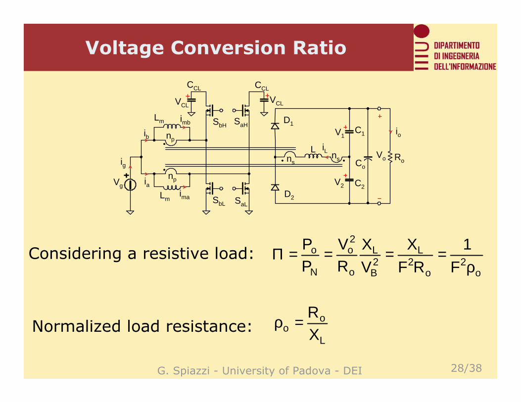
Voltage Conversion Ratio
o2
o2
L2B
L
o
2o
N
o
F
1
RF
X
V
XRV
PP
ρ====ΠConsidering a resistive load:
L
oo X
R=ρNormalized load resistance:
V2
V1
D1
L
SbL
Vo
C2
C1
SaL
Vg
iL
ia
io
D2
np
npib
SbH SaHLm imb
Lmima
nsnsig
VCL
CCL CCL
VCL
RoCo
G. Spiazzi - University of Padova - DEI 29/38
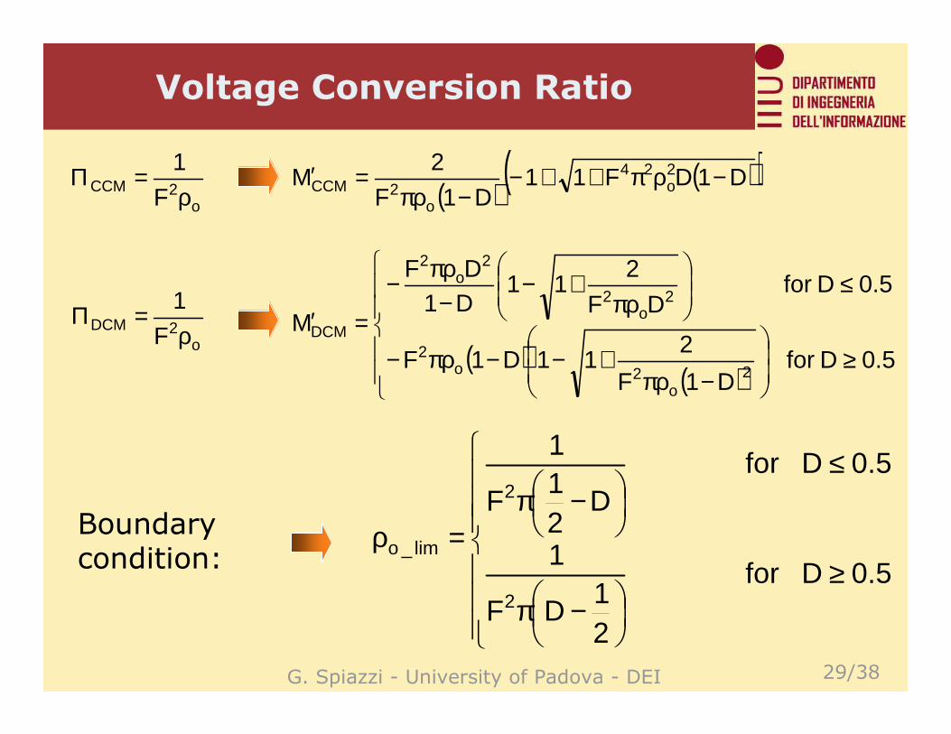
Voltage Conversion Ratio
o2CCM
F
1
ρ=Π
o2DCM
F
1
ρ=Π
Boundary condition:
( )( )( )D1DF11
D1F
2M 2
o24
o2CCM −ρπ++−
−πρ=′
( )( )
≥
−πρ+−−πρ−
≤
πρ+−
−πρ−
=′0.5D for
D1F
211D1F
0.5D for DF
211
D1DF
M
2o
2o2
2o
2
2o
2
DCM
≥
−π
≤
−π=ρ
0.5D for
21
DF
1
0.5D for D
21
F
1
2
2
lim_o
G. Spiazzi - University of Padova - DEI 30/38
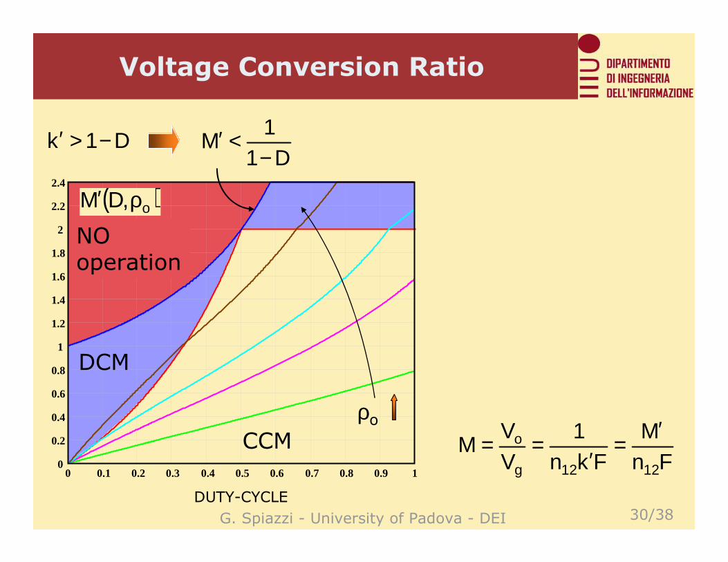
Voltage Conversion Ratio
0 0.1 0.2 0.3 0.4 0.5 0.6 0.7 0.8 0.9 10
0.2
0.4
0.6
0.8
1
1.2
1.4
1.6
1.8
2
2.2
2.4
DUTY-CYCLE
ρoCCM
DCM
( )o,DM ρ′
NO operation
FnM
Fkn1
VV
M1212g
o ′=
′==
D1k −>′D1
1M
−<′
G. Spiazzi - University of Padova - DEI 31/38
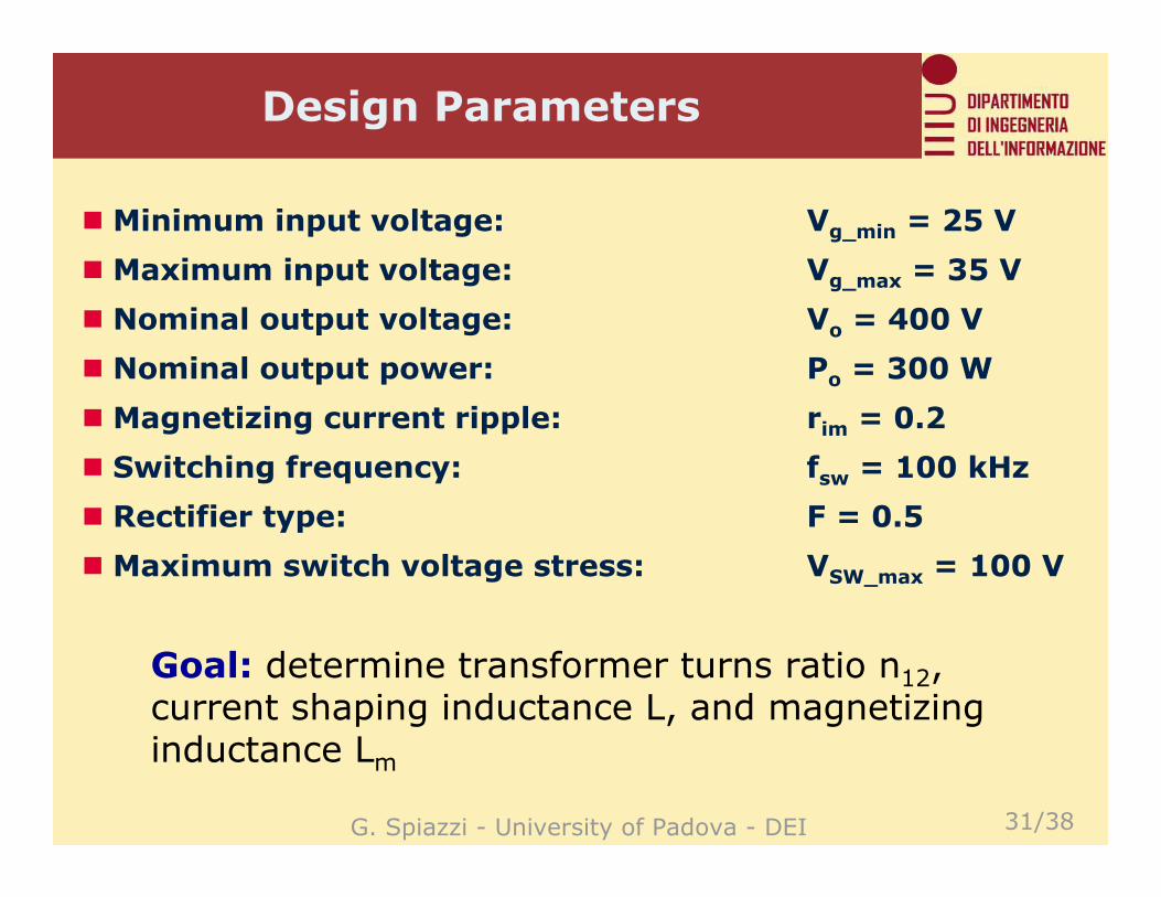
Design Parameters
� Minimum input voltage: Vg_min = 25 V
� Maximum input voltage: Vg_max = 35 V
� Nominal output voltage: Vo = 400 V
� Nominal output power: Po = 300 W
� Magnetizing current ripple: rim = 0.2
� Switching frequency: fsw = 100 kHz
� Rectifier type: F = 0.5
� Maximum switch voltage stress: VSW_max = 100 V
Goal: determine transformer turns ratio n12, current shaping inductance L, and magnetizing inductance Lm
G. Spiazzi - University of Padova - DEI 32/38
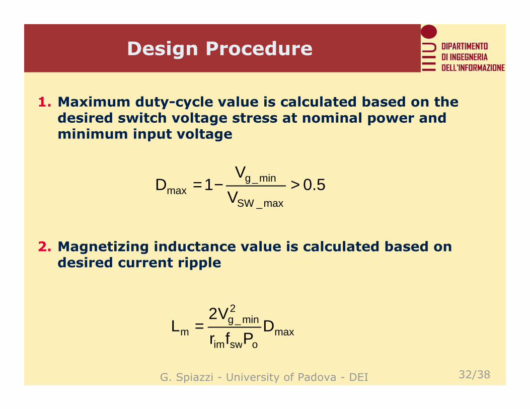
Design Procedure
1. Maximum duty-cycle value is calculated based on the desired switch voltage stress at nominal power and minimum input voltage
5.0V
V1D
max_SW
min_gmax >−=
maxoswim
2min_g
m DPfr
V2L =
2. Magnetizing inductance value is calculated based on desired current ripple
G. Spiazzi - University of Padova - DEI 33/38
Design Procedure
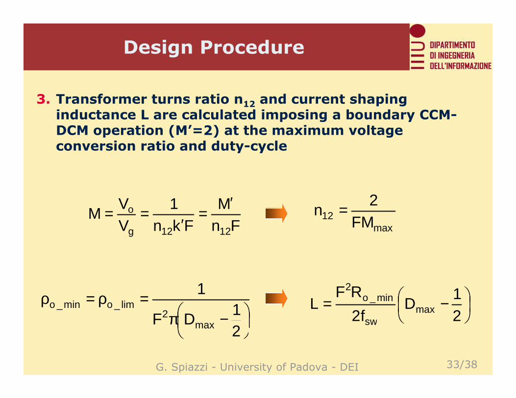
3. Transformer turns ratio n12 and current shaping inductance L are calculated imposing a boundary CCM-DCM operation (M’=2) at the maximum voltage conversion ratio and duty-cycle
max12 FM
2n =
FnM
Fkn1
VV
M1212g
o ′=
′==
21
DF
1
max2
lim_omin_o
−π=ρ=ρ
−=21
Df2
RFL max
sw
min_o2
G. Spiazzi - University of Padova - DEI 34/38
Design Procedure
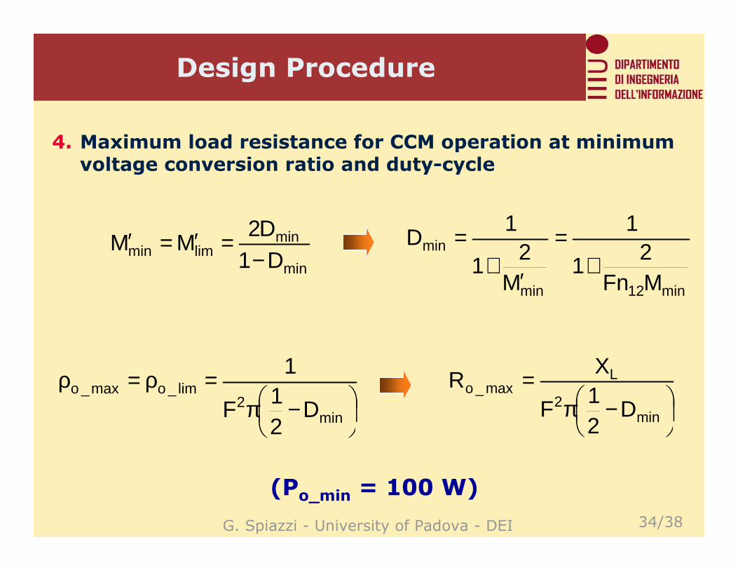
4. Maximum load resistance for CCM operation at minimum voltage conversion ratio and duty-cycle
min
minlimmin D1
D2MM
−=′=′
min12min
min
MFn2
1
1
M2
1
1D
+=
′+
=
−π=
min2
Lmax_o
D21
F
XR
D21
F
1
min2
lim_omax_o
−π=ρ=ρ
(Po_min = 100 W)
G. Spiazzi - University of Padova - DEI 35/38
Design Procedure
Voltage conversion ratio M’
0 0.1 0.2 0.3 0.4 0.5 0.6 0.7 0.8 0.9 10
0.2
0.4
0.6
0.8
1
1.2
1.4
1.6
1.8
2
2.2
2.4
CCM
DCM
( )o,DM ρ′
DmaxDmin
M’max
M’min
ρo_max ρo_min
Duty-cycle
G. Spiazzi - University of Padova - DEI 36/38
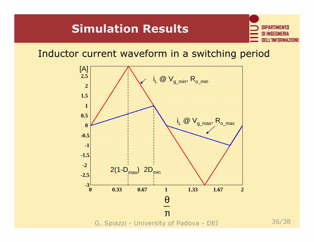
Simulation Results
Inductor current waveform in a switching period
0 0.33 0.67 1 1.33 1.67 2-3
-2.5
-2
-1.5
-1
-0.5
0
0.5
1
1.5
2
2.5[A]
iL @ Vg_min, Ro_min
iL @ Vg_max, Ro_max
πθ
2(1-Dmax) 2Dmin
G. Spiazzi - University of Padova - DEI 37/38
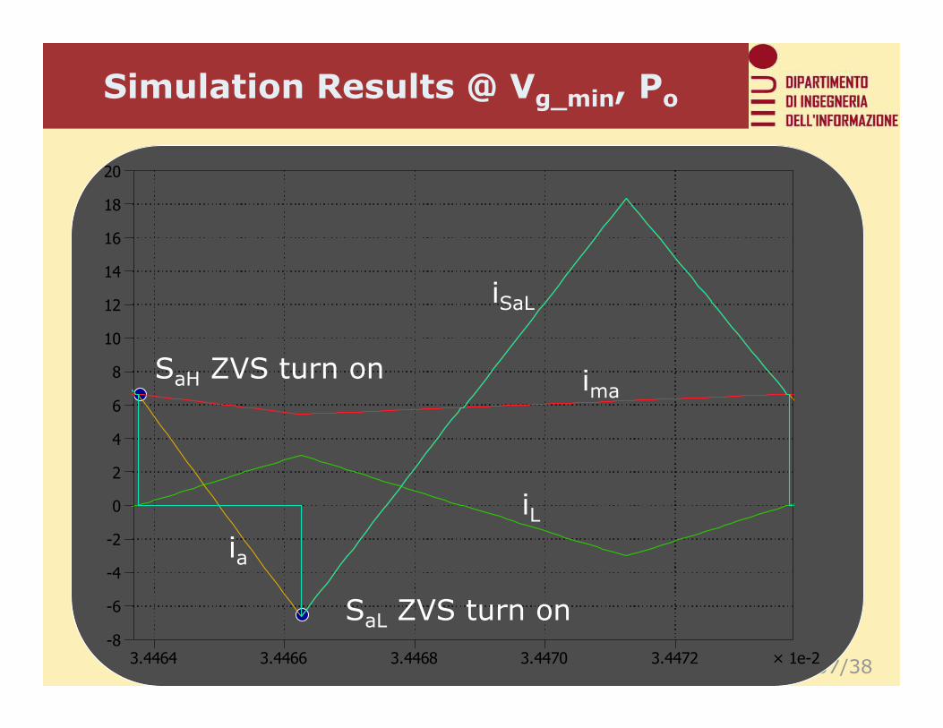
Simulation Results @ Vg_min, Po
× 1e-23.4464 3.4466 3.4468 3.4470 3.4472
-8
-6
-4
-2
0
2
4
6
8
10
12
14
16
18
20
iL
ia
ima
iSaL
SaL ZVS turn on
SaH ZVS turn on
G. Spiazzi - University of Padova - DEI 38/38
Conclusions
� The Interleaved Boost with Coupled Inductors converter operation was analyzed in normalized form
� The voltage conversion ratio was derived for both CCM and DCM operation
� A design procedure has been developed and verified by simulation