Embed Size (px)
Citation preview
Industr ia l & Mult imarket
Data Sheet Revision 2.0, 2012-06-14
ISO1I811TIsolated 8 Channel Digital Input with IEC61131-2 Type 1/2/3 Characteristics
ISOFACE™
Edition 2012-06-14Published byInfineon Technologies AG81726 Munich, Germany© 2012 Infineon Technologies AGAll Rights Reserved.
Legal DisclaimerThe information given in this document shall in no event be regarded as a guarantee of conditions or characteristics. With respect to any examples or hints given herein, any typical values stated herein and/or any information regarding the application of the device, Infineon Technologies hereby disclaims any and all warranties and liabilities of any kind, including without limitation, warranties of non-infringement of intellectual property rights of any third party.
InformationFor further information on technology, delivery terms and conditions and prices, please contact the nearest Infineon Technologies Office (www.infineon.com).
WarningsDue to technical requirements, components may contain dangerous substances. For information on the types in question, please contact the nearest Infineon Technologies Office.Infineon Technologies components may be used in life-support devices or systems only with the express written approval of Infineon Technologies, if a failure of such components can reasonably be expected to cause the failure of that life-support device or system or to affect the safety or effectiveness of that device or system. Life support devices or systems are intended to be implanted in the human body or to support and/or maintain and sustain and/or protect human life. If they fail, it is reasonable to assume that the health of the user or other persons may be endangered.
Data Sheet 3 Revision 2.0, 2012-06-14
ISO1I811T
ISO1I811T Revision History: 2012-06-14, Revision 2.0Previous Version: Preliminary Data Sheet V1.0Page Subjects (major changes since last revision)V2.0 Data SheetPage 25 Parallel Interface timing table updatedPage 26 Serial Interface timing table updated
ISO1I811T
Data Sheet 4 Revision 2.0, 2012-06-14
1 Pin Configuration and Functionality . . . . . . . . . . . . . . . . . . . . . . . . . . . . . . . . . . . . . . . . . . . . . . . . . 61.1 Pin Configuration . . . . . . . . . . . . . . . . . . . . . . . . . . . . . . . . . . . . . . . . . . . . . . . . . . . . . . . . . . . . . . . . . 61.2 Pin Functionality . . . . . . . . . . . . . . . . . . . . . . . . . . . . . . . . . . . . . . . . . . . . . . . . . . . . . . . . . . . . . . . . . . 81.2.1 Pins of Sensor Interface . . . . . . . . . . . . . . . . . . . . . . . . . . . . . . . . . . . . . . . . . . . . . . . . . . . . . . . . . . 81.2.2 Pins of Serial and Parallel logic Interface . . . . . . . . . . . . . . . . . . . . . . . . . . . . . . . . . . . . . . . . . . . . . 9
2 Blockdiagram . . . . . . . . . . . . . . . . . . . . . . . . . . . . . . . . . . . . . . . . . . . . . . . . . . . . . . . . . . . . . . . . . . 10
3 Functional Description . . . . . . . . . . . . . . . . . . . . . . . . . . . . . . . . . . . . . . . . . . . . . . . . . . . . . . . . . . . 113.1 Introduction . . . . . . . . . . . . . . . . . . . . . . . . . . . . . . . . . . . . . . . . . . . . . . . . . . . . . . . . . . . . . . . . . . . . . 113.2 Power Supply . . . . . . . . . . . . . . . . . . . . . . . . . . . . . . . . . . . . . . . . . . . . . . . . . . . . . . . . . . . . . . . . . . . 113.3 Internal Oscillator . . . . . . . . . . . . . . . . . . . . . . . . . . . . . . . . . . . . . . . . . . . . . . . . . . . . . . . . . . . . . . . . 123.4 Sensor Input . . . . . . . . . . . . . . . . . . . . . . . . . . . . . . . . . . . . . . . . . . . . . . . . . . . . . . . . . . . . . . . . . . . . 123.5 Common Error Output . . . . . . . . . . . . . . . . . . . . . . . . . . . . . . . . . . . . . . . . . . . . . . . . . . . . . . . . . . . . 143.6 Programmable Digital Input Filter . . . . . . . . . . . . . . . . . . . . . . . . . . . . . . . . . . . . . . . . . . . . . . . . . . . . 143.7 Parallel Interface Mode . . . . . . . . . . . . . . . . . . . . . . . . . . . . . . . . . . . . . . . . . . . . . . . . . . . . . . . . . . . . 153.8 Serial Interface Mode . . . . . . . . . . . . . . . . . . . . . . . . . . . . . . . . . . . . . . . . . . . . . . . . . . . . . . . . . . . . . 16
4 Standard Compliance . . . . . . . . . . . . . . . . . . . . . . . . . . . . . . . . . . . . . . . . . . . . . . . . . . . . . . . . . . . . 17
5 Electrical Characteristics . . . . . . . . . . . . . . . . . . . . . . . . . . . . . . . . . . . . . . . . . . . . . . . . . . . . . . . . . 195.1 Absolute Maximum Ratings . . . . . . . . . . . . . . . . . . . . . . . . . . . . . . . . . . . . . . . . . . . . . . . . . . . . . . . . 195.2 Operating Conditions and Power Supply . . . . . . . . . . . . . . . . . . . . . . . . . . . . . . . . . . . . . . . . . . . . . . 205.3 Electrical Characteristics Input Side . . . . . . . . . . . . . . . . . . . . . . . . . . . . . . . . . . . . . . . . . . . . . . . . . . 225.4 Electrical Characteristics Microcontroller Interface . . . . . . . . . . . . . . . . . . . . . . . . . . . . . . . . . . . . . . . 24
6 Package Outline . . . . . . . . . . . . . . . . . . . . . . . . . . . . . . . . . . . . . . . . . . . . . . . . . . . . . . . . . . . . . . . . 27
ISO1I811T
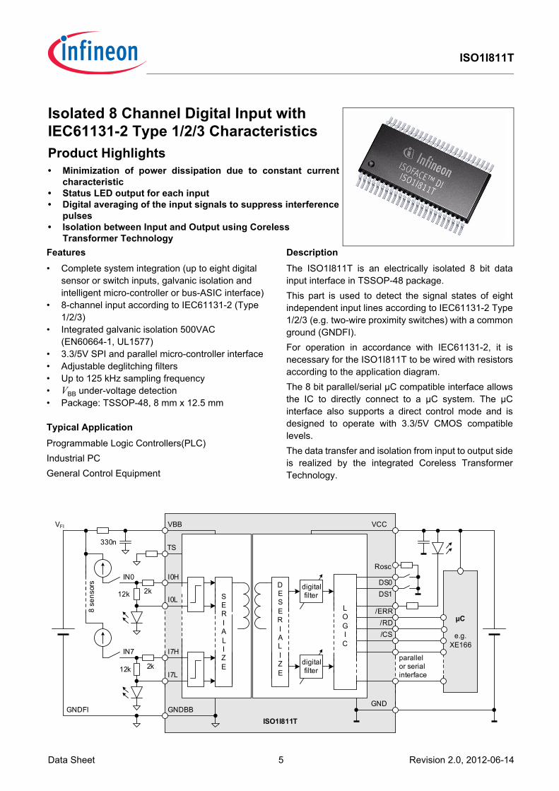
Isolated 8 Channel Digital Input with IEC61131-2 Type 1/2/3 CharacteristicsProduct Highlights• Minimization of power dissipation due to constant current
characteristic• Status LED output for each input• Digital averaging of the input signals to suppress interference
pulses• Isolation between Input and Output using Coreless
Transformer TechnologyFeatures• Complete system integration (up to eight digital
sensor or switch inputs, galvanic isolation and intelligent micro-controller or bus-ASIC interface)
• 8-channel input according to IEC61131-2 (Type 1/2/3)
• Integrated galvanic isolation 500VAC (EN60664-1, UL1577)
• 3.3/5V SPI and parallel micro-controller interface• Adjustable deglitching filters• Up to 125 kHz sampling frequency• VBB under-voltage detection• Package: TSSOP-48, 8 mm x 12.5 mm
Typical ApplicationProgrammable Logic Controllers(PLC)Industrial PCGeneral Control Equipment
DescriptionThe ISO1I811T is an electrically isolated 8 bit datainput interface in TSSOP-48 package.This part is used to detect the signal states of eightindependent input lines according to IEC61131-2 Type1/2/3 (e.g. two-wire proximity switches) with a commonground (GNDFI). For operation in accordance with IEC61131-2, it isnecessary for the ISO1I811T to be wired with resistorsaccording to the application diagram. The 8 bit parallel/serial µC compatible interface allowsthe IC to directly connect to a µC system. The µCinterface also supports a direct control mode and isdesigned to operate with 3.3/5V CMOS compatiblelevels. The data transfer and isolation from input to output sideis realized by the integrated Coreless TransformerTechnology.
µC
e.g. XE166
I0H
I0L
GNDBB
I7H
I7L
VBB VCC
TS
/ERR
/CS/RD
GND
SERIALIZE
DESERIALIZE
LOGIC
ISO1I811T
parallelor serialinterface
digitalfilter
digitalfilter
8 se
nsor
s
2k12k
330n
2k12k
IN0
IN7
VFI
GNDFI
DS0DS1
Rosc
Data Sheet 5 Revision 2.0, 2012-06-14
ISO1I811T
Pin Configuration and Functionality
1 Pin Configuration and FunctionalityThe pin configuration slightly differs for the parallel or the serial interface.
1.1 Pin ConfigurationThe ordering, type and functions of the IC pins are listed in the Table 1.
Table 1 Pin ConfigurationPin Parallel Interface Mode Serial Interface Mode
Symbol Ctrl1)
Type2)
Function Symbol Ctrl. Type Function
1 GND A Logic Ground GND2 SEL I PU Serial Parallel Mode Select SEL3 n.c. not connected n.c.4 ROSC A Clock Frequency Adjustment ROSC5 VCC A Positive 5/3.3V logic supply VCC6 ERR O OD,
PUError output ERR
7 GND A Logic Ground GND8 D0 O PPZ Data output bit0 SDI I PD SPI Data input9 D1 O PPZ Data output bit1 GND10 D2 O PPZ Data output bit2 GND11 D3 O PPZ Data output bit3 GND12 D4 O PPZ Data output bit4 GND13 D5 O PPZ Data output bit5 SCLK I PD SPI Shift Clock input14 D6 O PPZ Data output bit6 GND15 D7 O PPZ Data output bit7 SDO O PPZ SPI Data output16 CS I PU Chip Select CS17 RD I PU Data Read Input n.c. not connected18 GND A Logic Ground GND19 DS0 I PD Filter Select Input 0 DS020 DS1 I PD Filter Select Input 1 DS121 GND A Logic Ground GND22 n.c. not connected n.c.23 n.c. not connected n.c.24 GND A Logic Ground GND25 GNDBB A Input Ground GNDBB26 VBB A Positive input supply voltage VBB27 I0L A Input 0 Low, LED Out I0L28 I0H A Input 0 High I0H29 I1L A Input 1 Low, LED Out I1L30 I1H A Input 1 High I1H31 GNDBB A Input Ground GNDBB32 I2L A Input 2 Low, LED Out I2L
Data Sheet 6 Revision 2.0, 2012-06-14
ISO1I811T
Pin Configuration and Functionality
33 I2H A Input 2 High I2H34 I3L A Input 3 Low, LED Out I3L35 I3H A Input 3 High I3H36 TS A Sensor Type 1/2/3 Select TS37 GNDBB A Input Ground GNDBB38 n.c. not connected n.c.39 I4L A Input 4 Low, LED Out I4L40 I4H A Input 4 High I4H41 I5L A Input 5 Low, LED Out I5L42 I5H A Input 5 High I5H33 GNDBB A Input Ground GNDBB44 I6L A Input 6 Low, LED Out I6L45 I6H A Input 6 High I6H46 I7L A Input 7 Low, LED Out I7L47 I7H A Input 7 High I7H48 GNDBB A Input Ground GNDBB1) Direction of the pin: I = input, O = output, IO = Input/Output2) Type of the pin: A = analog, OD = Open-Drain, PU = internal Pull-Up resistor, PD = internal Pull-Down resistor,
PPZ = Push-Pull pin with High-Impedance functionality
Table 1 Pin ConfigurationPin Parallel Interface Mode Serial Interface Mode
Symbol Ctrl1)
Type2)
Function Symbol Ctrl. Type Function
Data Sheet 7 Revision 2.0, 2012-06-14
ISO1I811T
Pin Configuration and Functionality
Figure 1 TSSOP-48 Pinout for Parallel and Serial Interface
1.2 Pin FunctionalityThe meaning and the functions of the IC pins are described below.
1.2.1 Pins of Sensor InterfaceVBB (Positive supply 9.6-35V sensor supply)VBB supplies the sensor input stage. GNDBB (Ground for VBB domain)This pin acts as the ground reference for the sensor input stage, that is supplied by VBB.I0H... I7H (Input channel 0 ... 7)Sensor inputs with current sink characteristic according IEC61131-2 Type 1/2/3 which has been selected by pin TSI0L... I7L (LED output channel 0 ... 7)This pin provides the output signal to switch on the LED if the input voltage and current has been detected as“High” according the selected type.TS (Type Select)By connecting a resistor between TS and GNDBB the sensor type (Type 1/2/3) can be selected (refer to Table 9for corresponding resistor value). This pin is for static configuration (pin-strapping). The voltage level at pin TS isnot allowed to be changed during operation.
GND
SEL
n.c.
Rosc
/ERR
GND
D0
D1
D3
D4
D5
D6
D7
/CS
/RD
GND
D2
DS0
1
2
3
4
5
6
7
8
9
10
11
12
13
14
15
16
17
18
GNDBB
I6H
I6L
n.c.
I5H
I5L
I4H
GNDBB
GNDBB
I3H
I7H
I7L
I2H
I3L
I2L
I4L
TS36
35
34
33
32
31
30
29
28
27
26
25
Pinout for parallel Interface
DS1
VCC
GND
n.c.
n.c.
GND
19
20
21
22
23
24
I1H
I1L
I0L
I0H
VBB
GNDBB
44
43
42
41
40
39
38
37
48
47
46
45
1
2
3
4
5
6
7
8
9
10
11
12
13
14
15
16
17
18
36
35
34
33
32
31
30
29
28
27
26
25
Pinout for serial Interface
19
20
21
22
23
24
44
43
42
41
40
39
38
37
48
47
46
45
GND
SEL
n.c.
Rosc
/ERR
GND
SDI
GND
GND
GND
SCLK
GND
SDO
/CS
n.c.
GND
GND
DS0
DS1
VCC
GND
n.c.
n.c.
GND
n.c. = Not Connected
GNDBB
GNDBB
I6H
I6L
n.c.
I5H
I5L
I4H
GNDBB
GNDBB
I3H
I7H
I7L
I2H
I3L
I2L
I4L
TS
I1H
I1L
I0L
I0H
VBB
GNDBB
GNDBB
Data Sheet 8 Revision 2.0, 2012-06-14
ISO1I811T
Pin Configuration and Functionality1.2.2 Pins of Serial and Parallel logic InterfaceSome pins are common for both interface types, some others are specific for the parallel or serial access.VCC (Positive 3.3 / 5V logic supply) VCC supplies the output interface that is electrically isolated from the sensor input stage. The interface can besupplied with 3.3 / 5V.GND (Ground for VCC domain)This pin is the ground reference for the uC-interface that is supplied by VCC.ROSC (Clock Adjustment)A high precision resistor has to be connected between ROSC and GND to guarantee the frequency accuracy ofthe sampling clock. For details see Chapter 3.3.ERR (Error Output)The low active ERR signal contains the OR-wired information of the sensor input missing voltage (MV) detectionand the internal data transmission failure detection unit. The output pin ERR provides an open drain functionality.A current source is also connected to the pin ERR. In normal operation the signal ERR is high. See Chapter 3.5for more details. DS0, DS1 (Filter Select)The internal filter delay can be selected by pulling those pins to VCC or to GND (see Table 10). These pins arefor static configuration (pin-strapping).CS (Chip Select)When this pin is in a logic Low state, the IC interface is enabled and data can be transferred.
SEL (Serial or Parallel Mode Select)When this pin is in a logic High state, the IC operates in Serial Mode. For Parallel Mode operation the pin has tobe pulled into logic Low state. This pin has an internal Pull-UP resistor.
The following pins are provided by the parallel interface
D7:D0 (Data output bit7 ... bit0)The pins D0 .. D7 are the outputs for data read.RD (Read Select)By pulling this pin down, a read transaction is initiated on the data bus and the data becomes valid.
The following pins are provided by the serial interface
SCLK (Serial interface shift clock)Output data is updated with the falling edge of this input clock signal.SDI (Serial interface input data)SDI is put into a FIFO dedicated to the sensor data bits (no internal registers Write operation supported, only daisychain). Input data is sampled with the rising edge of SCLK.SDO (Serial interface data)SDO provides the sensor data bits.
Data Sheet 9 Revision 2.0, 2012-06-14
ISO1I811T
Blockdiagram
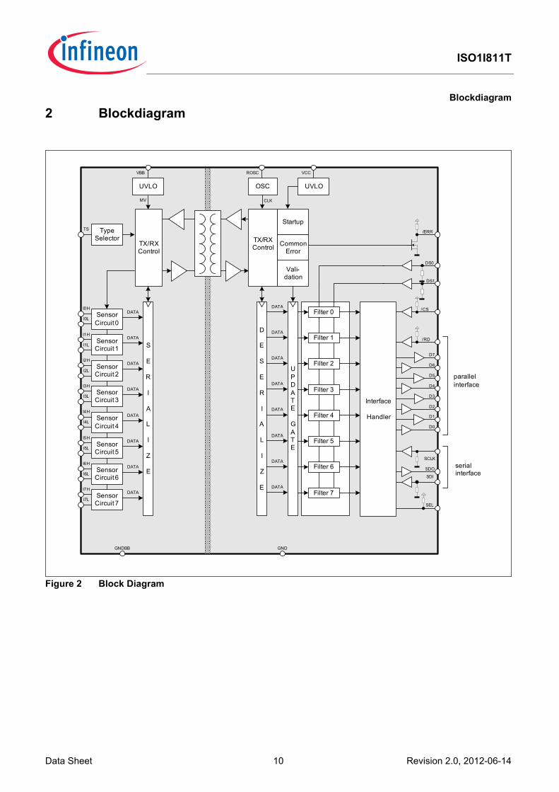
2 Blockdiagram
Figure 2 Block Diagram
I1H
I1L
I2H
I2L
I3H
I3L
I4H
I4L
I5H
I5L
I6H
I6L
I7H
I7L
SensorCircuit 0
I0H
I0L
GNDBB
DATA
DATA
DATA
DATA
DATA
DATA
DATA
DATA
S
E
R
I
A
L
I
Z
E
MV
D
E
S
E
R
I
A
L
I
Z
E
UPDATE
GATE
/ERR
Interface
Handler
/CS
/RD
SDI
D7
D6
D5
D4
D3
D2
D1
D0
SCLK
SDO
parallelinterface
serialinterface
GND
UVLO
VCC
Vali-dation
UVLO
VBB
TX/RX Control
TS Type Selector
SensorCircuit 1
SensorCircuit 2
SensorCircuit 3
SensorCircuit 4
SensorCircuit 5
SensorCircuit 6
SensorCircuit 7
DS0
TX/RX Control
DATA
DATA
DATA
DATA
DATA
DATA
DATA
DATAFilter 7
Filter 6
Filter 5
Filter 4
Filter 3
Filter 2
Filter 1
Filter 0
Startup
Common Error
OSC
CLK
ROSC
DS1
SEL
Data Sheet 10 Revision 2.0, 2012-06-14
ISO1I811T
Functional Description
3 Functional DescriptionThe ISO1I811T is an electrically isolated 8 bit data input interface. This part is used to detect the signal states ofeight independent input lines according to IEC61131-2 Type 1/2/3 (e.g. two-wire proximity switches) with acommon ground (GNDBB).
3.1 IntroductionThe current in the input circuit is determined by the switching element in state “0” and by characteristics of the inputstage in state “1”.The octal input device is intended for a configuration comprising of two specified external resistors per channel,as shown in Figure 5 “Typical Application for Sensor Input Type 1, 2, and 3” on Page 13. As a result thepower dissipation within the package is at a minimum.The voltage dependent current through the external resistor REXT is compensated by a negative differentialresistance of the current sink across pins IxH and IxL, therefore input INx behaves like a constant current sink.The comparator assigns level 1 or 0 to the voltage present at input IxH. To improve interference protection, thecomparator is provided with hysteresis. A status LED is connected in series with the input circuit (REXT and currentsink). If no LED is used an external resistor of 2 kΩ should be connected between IxL and GNDBB. The specifiedswitching thresholds may change if the resistor is used.The LED drive short-circuits the status LED if the comparator detects “0”. A constant current sink in parallel withthe LED reduces the operating current of the LED, and a voltage limiter ensures that the input circuit remainsoperational if the LED is interrupted, but the specified switching thresholds may change.For each channel an adjustable digital filter is provided which samples the comparator signal at a rate selected bythe pins DS0 and DS1. The digital filter is designed to provide averaging characteristics. If the input value remainsthe same for the selected number of sampling values, then the output changes to the corresponding state.The control interface is compatible to standard microcontrollers. Furthermore a direct control mode can beselected that allows the direct control of the outputs D0...D7 by means of the inputs I0H...I7H without any additionallogic signal. The µC compatible interfaces allows a direct connection to the ports of a microcontroller without theneed for other components. The diagnostic logic on the chip monitors the internal data transfer as well as thesensor input supply. The information is sent via the internal coreless transformer to the pin ERR at the µC-Interfaceside.
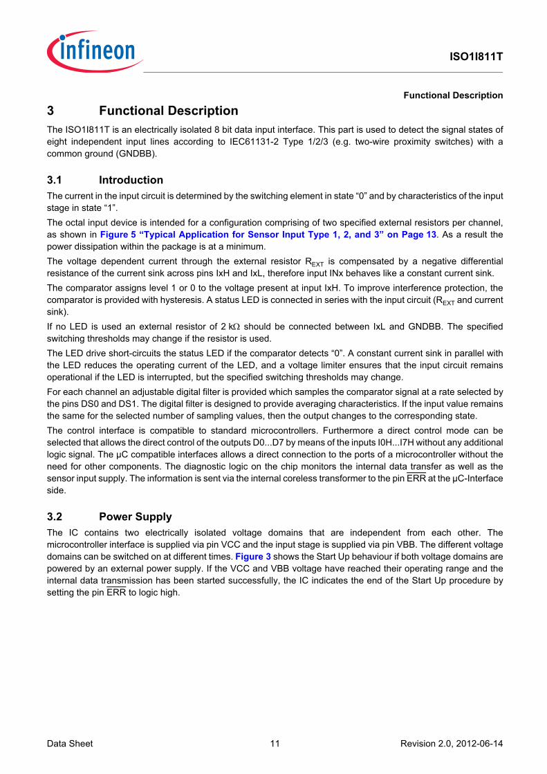
3.2 Power SupplyThe IC contains two electrically isolated voltage domains that are independent from each other. Themicrocontroller interface is supplied via pin VCC and the input stage is supplied via pin VBB. The different voltagedomains can be switched on at different times. Figure 3 shows the Start Up behaviour if both voltage domains arepowered by an external power supply. If the VCC and VBB voltage have reached their operating range and theinternal data transmission has been started successfully, the IC indicates the end of the Start Up procedure bysetting the pin ERR to logic high.
Data Sheet 11 Revision 2.0, 2012-06-14
ISO1I811T
Functional Description
Figure 3 Start-Up
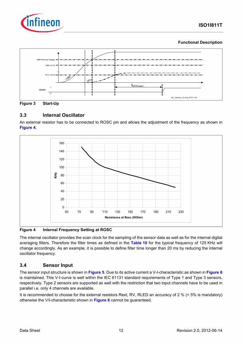
3.3 Internal OscillatorAn external resistor has to be connected to ROSC pin and allows the adjustment of the frequency as shown inFigure 4.
Figure 4 Internal Frequency Setting at ROSC
The internal oscillator provides the scan clock for the sampling of the sensor data as well as for the internal digitalaveraging filters. Therefore the filter times as defined in the Table 10 for the typical frequency of 125 KHz willchange accordingly. As an example, it is possible to define filter time longer than 20 ms by reducing the internaloscillator frequency.
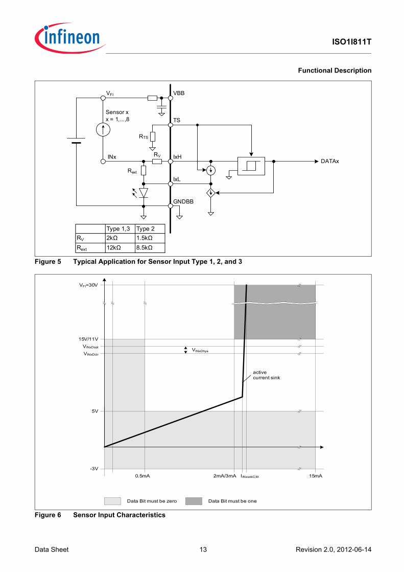
3.4 Sensor InputThe sensor input structure is shown in Figure 5. Due to its active current a V-I-characteristic as shown in Figure 6is maintained. This V-I-curve is well within the IEC 61131 standard requirements of Type 1 and Type 3 sensors,respectively. Type 2 sensors are supported as well with the restriction that two input channels have to be used inparallel i.e. only 4 channels are available. It is recommended to choose for the external resistors Rext, RV, RLED an accuracy of 2 % (< 5% is mandatory)otherwise the V/I-characteristic shown in Figure 6 cannot be guaranteed.
tds_startup_timing_STD.vsd
VBB
VBB UVLO
/ERR
VBB Missing Voltage
VCC
VCC UVLO
1
0
tERRstart
0
20
40
60
80
100
120
140
160
50 70 90 110 130 150 170 190 210 230
Resistance at Rosc (KOhm)
KHz
Data Sheet 12 Revision 2.0, 2012-06-14
ISO1I811T
Functional Description
Figure 5 Typical Application for Sensor Input Type 1, 2, and 3
Figure 6 Sensor Input Characteristics
Rext
RVINx IxH
IxL
DATAx
VFI VBB
GNDBB
Sensor xx = 1,...,8
RTS
TS
Type 1,3 Type 2RV 2kΩ 1.5kΩRext 12kΩ 8.5kΩ
-3V
5V
15V/11V
0.5mA 2mA/3mA 15mA
VINxDset
VINxDclr
IINxsnkC,M
VFI=30V
Data Bit must be zero Data Bit must be one
active current sink
VINxDhys
Data Sheet 13 Revision 2.0, 2012-06-14
ISO1I811T
Functional Description
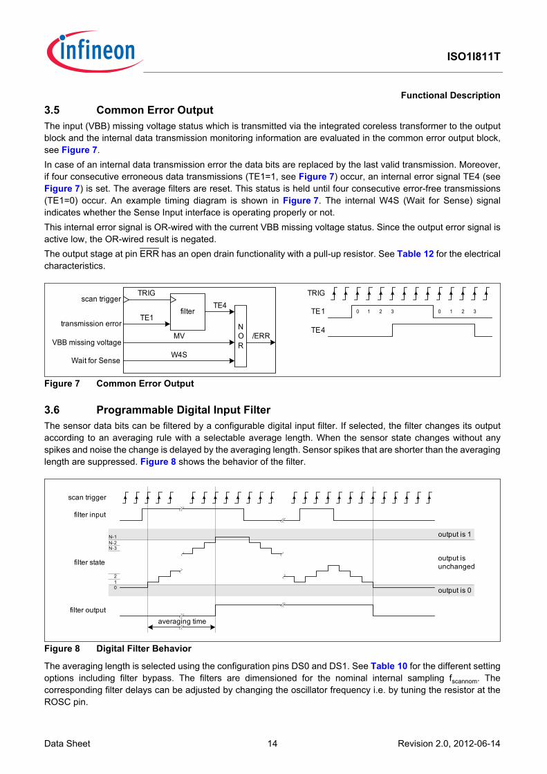
3.5 Common Error OutputThe input (VBB) missing voltage status which is transmitted via the integrated coreless transformer to the outputblock and the internal data transmission monitoring information are evaluated in the common error output block,see Figure 7. In case of an internal data transmission error the data bits are replaced by the last valid transmission. Moreover,if four consecutive erroneous data transmissions (TE1=1, see Figure 7) occur, an internal error signal TE4 (seeFigure 7) is set. The average filters are reset. This status is held until four consecutive error-free transmissions(TE1=0) occur. An example timing diagram is shown in Figure 7. The internal W4S (Wait for Sense) signalindicates whether the Sense Input interface is operating properly or not.This internal error signal is OR-wired with the current VBB missing voltage status. Since the output error signal isactive low, the OR-wired result is negated.The output stage at pin ERR has an open drain functionality with a pull-up resistor. See Table 12 for the electricalcharacteristics.
Figure 7 Common Error Output
3.6 Programmable Digital Input FilterThe sensor data bits can be filtered by a configurable digital input filter. If selected, the filter changes its outputaccording to an averaging rule with a selectable average length. When the sensor state changes without anyspikes and noise the change is delayed by the averaging length. Sensor spikes that are shorter than the averaginglength are suppressed. Figure 8 shows the behavior of the filter.
Figure 8 Digital Filter Behavior
The averaging length is selected using the configuration pins DS0 and DS1. See Table 10 for the different settingoptions including filter bypass. The filters are dimensioned for the nominal internal sampling fscannom. Thecorresponding filter delays can be adjusted by changing the oscillator frequency i.e. by tuning the resistor at theROSC pin.
filter
NOR
scan trigger
transmission errorMV
TRIG
TE1TE1
TE4
VBB missing voltage
TRIG
TE4
0 1 2 3 0 1 2 3
/ERR
W4SWait for Sense
scan trigger
filter input
filter output
filter state
output is 1
output is 0
output isunchanged
012
N-1N-2
averaging time
N-3
Data Sheet 14 Revision 2.0, 2012-06-14
ISO1I811T
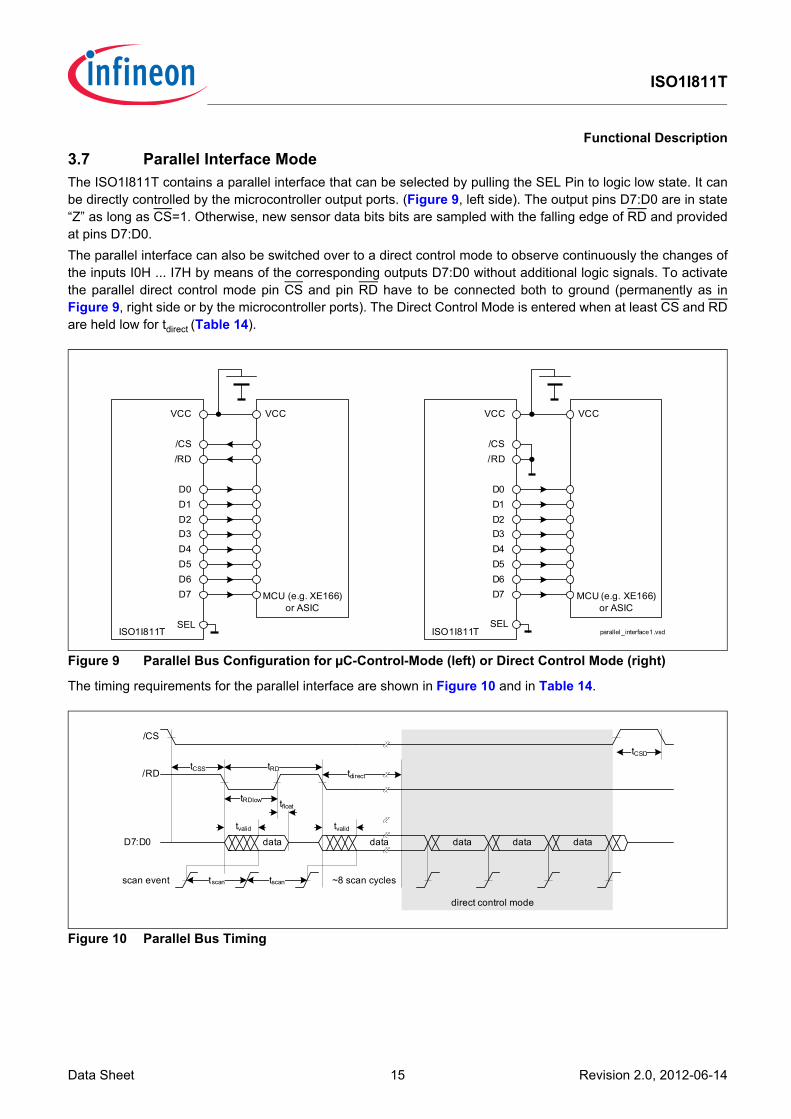
Functional Description3.7 Parallel Interface ModeThe ISO1I811T contains a parallel interface that can be selected by pulling the SEL Pin to logic low state. It canbe directly controlled by the microcontroller output ports. (Figure 9, left side). The output pins D7:D0 are in state“Z” as long as CS=1. Otherwise, new sensor data bits bits are sampled with the falling edge of RD and providedat pins D7:D0. The parallel interface can also be switched over to a direct control mode to observe continuously the changes ofthe inputs I0H ... I7H by means of the corresponding outputs D7:D0 without additional logic signals. To activatethe parallel direct control mode pin CS and pin RD have to be connected both to ground (permanently as inFigure 9, right side or by the microcontroller ports). The Direct Control Mode is entered when at least CS and RDare held low for tdirect (Table 14).
Figure 9 Parallel Bus Configuration for µC-Control-Mode (left) or Direct Control Mode (right)
The timing requirements for the parallel interface are shown in Figure 10 and in Table 14.
Figure 10 Parallel Bus Timing
VCC
/CS/RD
D0D1D2D3D4D5D6D7
ISO1I811T
MCU (e.g. XE166)or ASIC
VCC
/CS/RD
D0D1D2D3D4D5D6D7
ISO1I811T
MCU (e.g. XE166)or ASIC
parallel _interface1.vsd
VCCVCC
SEL SEL
/CS
tCSS/RD
D7:D0 data
tRD
data
direct control mode
tdirect
tvalid
tCSD
~8 scan cycles
tvalid
data datadata
tscanscan event tscan
tRDlow tfloat
Data Sheet 15 Revision 2.0, 2012-06-14
ISO1I811T
Functional Description
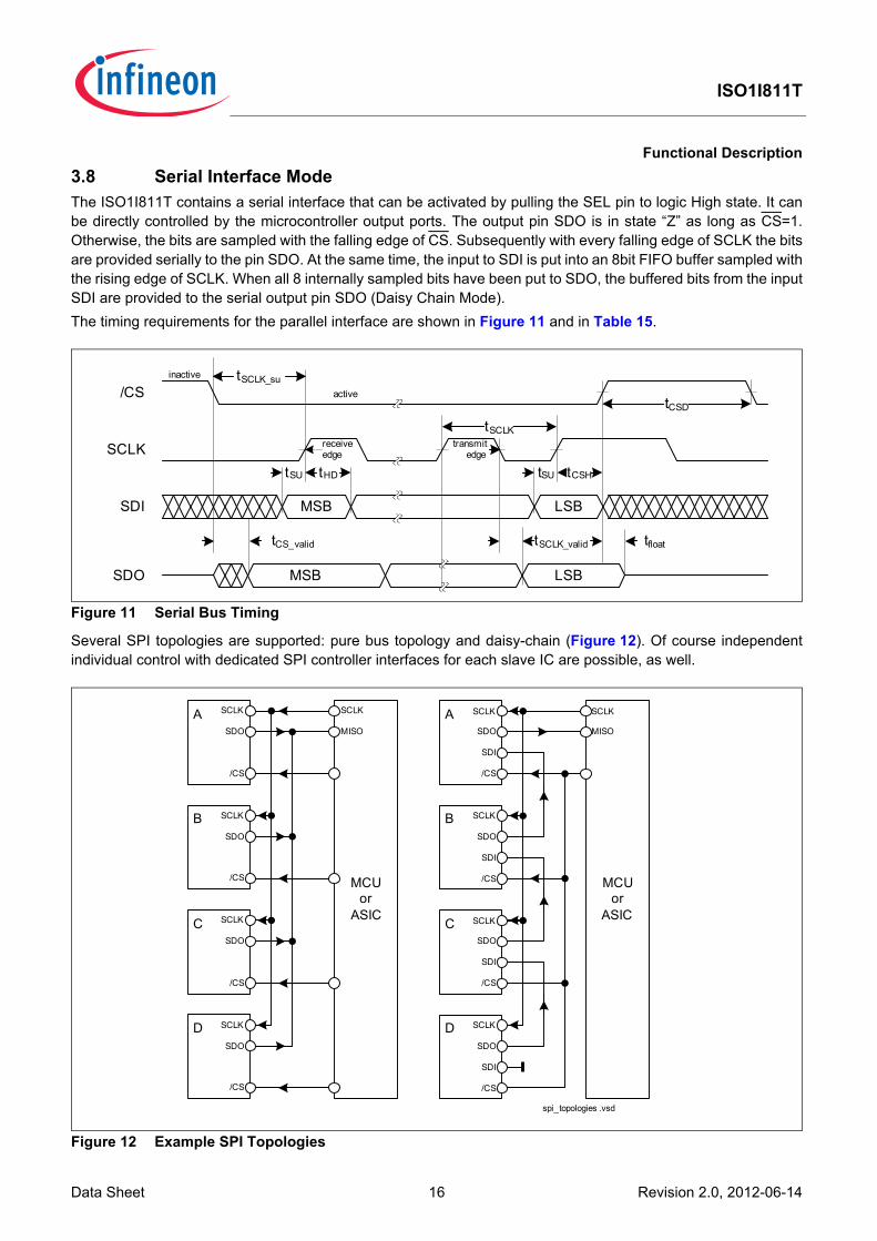
3.8 Serial Interface ModeThe ISO1I811T contains a serial interface that can be activated by pulling the SEL pin to logic High state. It canbe directly controlled by the microcontroller output ports. The output pin SDO is in state “Z” as long as CS=1.Otherwise, the bits are sampled with the falling edge of CS. Subsequently with every falling edge of SCLK the bitsare provided serially to the pin SDO. At the same time, the input to SDI is put into an 8bit FIFO buffer sampled withthe rising edge of SCLK. When all 8 internally sampled bits have been put to SDO, the buffered bits from the inputSDI are provided to the serial output pin SDO (Daisy Chain Mode). The timing requirements for the parallel interface are shown in Figure 11 and in Table 15.
Figure 11 Serial Bus Timing
Several SPI topologies are supported: pure bus topology and daisy-chain (Figure 12). Of course independentindividual control with dedicated SPI controller interfaces for each slave IC are possible, as well.
Figure 12 Example SPI Topologies
transmit edge
receive edge
tSCLK_valid
MSB
tSU tHD
/CS
SCLK
SDI
SDO
LSB
tSU tCSH
MSB LSB
tCSD
tfloattCS_valid
inactive
active
tSCLK
tSCLK_su
SCLK
/CS
SDO
A
SCLK
/CS
SDO
B
SCLK
/CS
SDO
C
SCLK
/CS
SDO
D
SCLK
/CS
SDO
SDI
A
SCLK
/CS
SDO
SDI
B
SCLK
/CS
SDO
SDI
C
SCLK
/CS
SDO
SDI
D
MCUor
ASIC
SCLK
MISO
MCUor
ASIC
SCLK
MISO
spi_topologies .vsd
Data Sheet 16 Revision 2.0, 2012-06-14
ISO1I811T
Standard Compliance
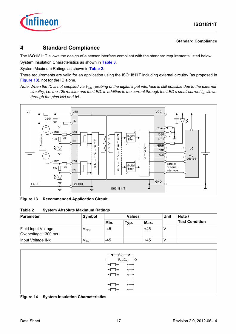
4 Standard ComplianceThe ISO1I811T allows the design of a sensor interface compliant with the standard requirements listed below:System Insulation Characteristics as shown in Table 3,System Maximum Ratings as shown in Table 2.There requirements are valid for an application using the ISO1I811T including external circuitry (as proposed inFigure 13), not for the IC alone.Note: When the IC is not supplied via VBB , probing of the digital input interface is still possible due to the external
circuitry, i.e. the 12k resistor and the LED. In addition to the current through the LED a small current IIxH flows through the pins IxH and IxL.
Figure 13 Recommended Application Circuit
Figure 14 System Insulation Characteristics
Table 2 System Absolute Maximum RatingsParameter Symbol Values Unit Note /
Test ConditionMin. Typ. Max.Field Input VoltageOvervoltage 1300 ms
VFIov -45 +45 V
Input Voltage INx VINx -45 +45 V
µC
e.g. XE166
I0H
I0L
GNDBB
I7H
I7L
VBB VCC
TS
/ERR
/CS/RD
GND
SERIALIZE
DESERIALIZE
LOGIC
ISO1I811T
parallelor serialinterface
digitalfilter
digitalfilter
8 se
nsor
s
2k12k
330n
2k12k
IN0
IN7
VFI
GNDFI
DS0DS1
Rosc
+ −
I OVISO
RIO,CIO
Data Sheet 17 Revision 2.0, 2012-06-14
ISO1I811T
Standard Compliance
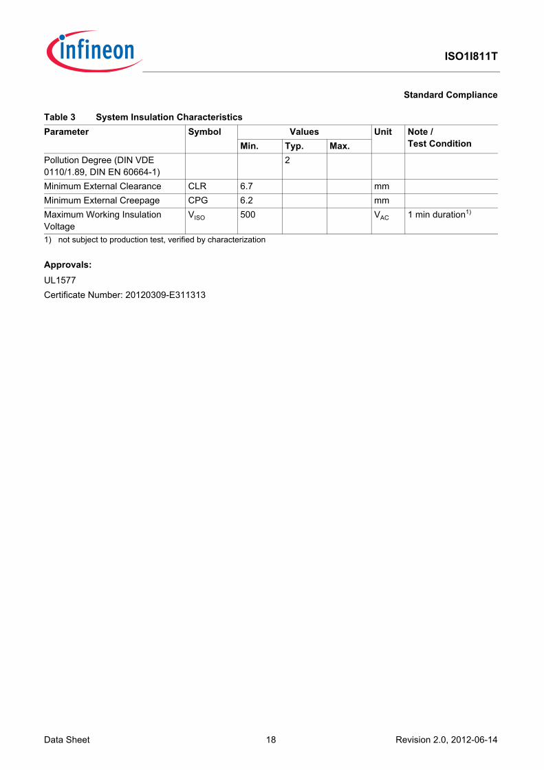
Approvals:UL1577Certificate Number: 20120309-E311313
Table 3 System Insulation CharacteristicsParameter Symbol Values Unit Note /
Test ConditionMin. Typ. Max.Pollution Degree (DIN VDE 0110/1.89, DIN EN 60664-1)
2
Minimum External Clearance CLR 6.7 mmMinimum External Creepage CPG 6.2 mmMaximum Working Insulation Voltage
VISO 500 VAC 1 min duration1)
1) not subject to production test, verified by characterization
Data Sheet 18 Revision 2.0, 2012-06-14
ISO1I811T
Electrical Characteristics
5 Electrical CharacteristicsThis section comprises: • Operating Conditions and Power Supply (see Section 5.2)• Electrical Characteristics Input Side (see Section 5.3)• Electrical Characteristics Microcontroller Interface (see Section 5.4)Tolerance values always contain the sum of process-related tolerance values and tolerance-values based on thetemperature drift within the specified temperature range.
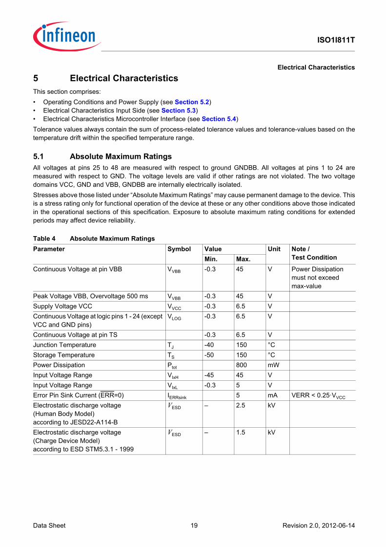
5.1 Absolute Maximum RatingsAll voltages at pins 25 to 48 are measured with respect to ground GNDBB. All voltages at pins 1 to 24 aremeasured with respect to GND. The voltage levels are valid if other ratings are not violated. The two voltagedomains VCC, GND and VBB, GNDBB are internally electrically isolated.Stresses above those listed under “Absolute Maximum Ratings” may cause permanent damage to the device. Thisis a stress rating only for functional operation of the device at these or any other conditions above those indicatedin the operational sections of this specification. Exposure to absolute maximum rating conditions for extendedperiods may affect device reliability.
Table 4 Absolute Maximum RatingsParameter Symbol Value Unit Note /
Test ConditionMin. Max.Continuous Voltage at pin VBB VVBB -0.3 45 V Power Dissipation
must not exceed max-value
Peak Voltage VBB, Overvoltage 500 ms VVBB -0.3 45 VSupply Voltage VCC VVCC -0.3 6.5 VContinuous Voltage at logic pins 1 - 24 (except VCC and GND pins)
VLOG -0.3 6.5 V
Continuous Voltage at pin TS -0.3 6.5 VJunction Temperature TJ -40 150 °CStorage Temperature TS -50 150 °CPower Dissipation Ptot 800 mWInput Voltage Range VIxH -45 45 VInput Voltage Range VIxL -0.3 5 VError Pin Sink Current (ERR=0) IERRsink 5 mA VERR < 0.25·VVCC
Electrostatic discharge voltage(Human Body Model)according to JESD22-A114-B
VESD – 2.5 kV
Electrostatic discharge voltage(Charge Device Model)according to ESD STM5.3.1 - 1999
VESD – 1.5 kV
Data Sheet 19 Revision 2.0, 2012-06-14
ISO1I811T
Electrical Characteristics
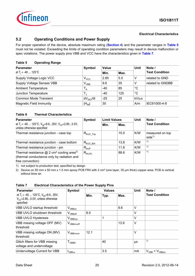
5.2 Operating Conditions and Power SupplyFor proper operation of the device, absolute maximum rating (Section 4) and the parameter ranges in Table 5must not be violated. Exceeding the limits of operating condition parameters may result in device malfunction orspec violations. The power supply pins VBB and VCC have the characteristics given in Table 7.
Table 5 Operating RangeParameterat Tj = -40 ... 125°C
Symbol Value Unit Note / Test ConditionMin. Max.
Supply Voltage Logic VCC VVCC 2.85 5.5 V related to GNDSupply Voltage Senses VBB VVBB 9.6 35 V related to GNDBBAmbient Temperature TA -40 85 °CJunction Temperature TJ -40 125 °CCommon Mode Transient dVISO/dt -25 25 kV/μsMagnetic Field Immunity |HIM| 30 A/m IEC61000-4-8
Table 6 Thermal CharacteristicsParameterat Tj = -40 ... 125°C, Vbb=9.6...35V, VCC=2.85...5.5V, unless otherwise specified
Symbol Limit Values Unit Note / Test ConditionMin. Max.
Thermal resistance junction - case top RthJC_Top 15.0 K/W measured on top side1)
1) not subject to production test, specified by design
Thermal resistance junction - case bottom RthJC_Bot 13.8 K/W 1)
Thermal resistance junction - pin RthJP 11.8 K/W 1)
Thermal resistance @ 2 cm² cooling area2)
(thermal conductance only by radiation and free convection)
2) Device on 50 mm x 50 mm x 1.5 mm epoxy PCB FR4 with 2 cm² (one layer, 35 µm thick) copper area. PCB is vertical without blow air.
Rth(JA) 88.6 K/W 1)
Table 7 Electrical Characteristics of the Power Supply PinsParameterat Tj = -40 ... 125°C, Vbb=9.6...35V, VCC=2.85...5.5V, unless otherwise specified
Symbol Values Unit Note / Test ConditionMin. Typ. Max.
VBB UVLO startup threshold VVBBon 9.6 VVBB UVLO shutdown threshold VVBBoff 8.0 VVBB UVLO Hysteresis VVBBhys 1 VVBB missing voltage OFF (MV) threshold
VVBBmvoff 13.9 V
VBB missing voltage ON (MV) threshold
VVBBmvon 12.1 V
Glitch filters for VBB missing voltage and undervoltage
TVBBfil 40 µs 1)
Undervoltage Current for VBB IVBBuv 3.5 mA VVBB < VVBBon
Data Sheet 20 Revision 2.0, 2012-06-14
ISO1I811T
Electrical Characteristics
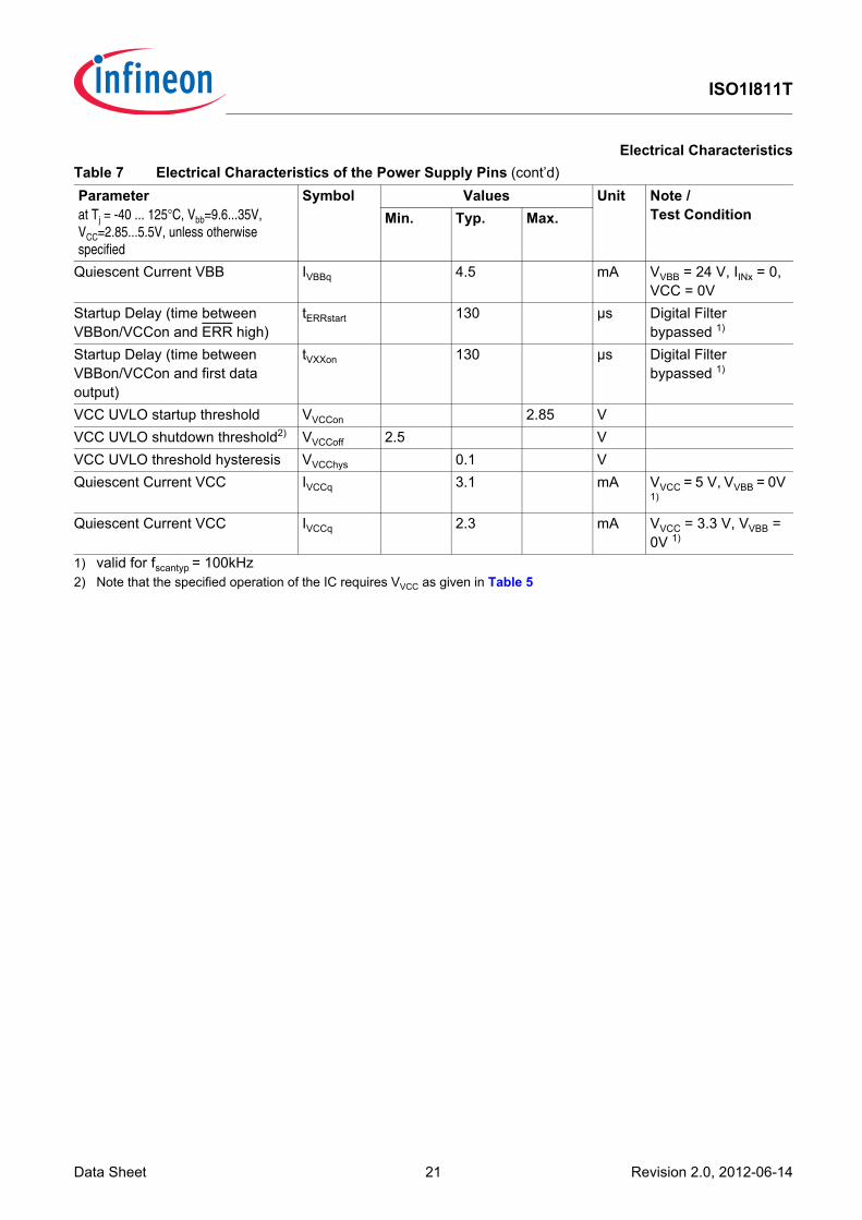
Quiescent Current VBB IVBBq 4.5 mA VVBB = 24 V, IINx = 0, VCC = 0V
Startup Delay (time between VBBon/VCCon and ERR high)
tERRstart 130 µs Digital Filter bypassed 1)
Startup Delay (time between VBBon/VCCon and first data output)
tVXXon 130 µs Digital Filter bypassed 1)
VCC UVLO startup threshold VVCCon 2.85 VVCC UVLO shutdown threshold2) VVCCoff 2.5 VVCC UVLO threshold hysteresis VVCChys 0.1 VQuiescent Current VCC IVCCq 3.1 mA VVCC = 5 V, VVBB = 0V
1)
Quiescent Current VCC IVCCq 2.3 mA VVCC = 3.3 V, VVBB = 0V 1)
1) valid for fscantyp = 100kHz2) Note that the specified operation of the IC requires VVCC as given in Table 5
Table 7 Electrical Characteristics of the Power Supply Pins (cont’d)Parameterat Tj = -40 ... 125°C, Vbb=9.6...35V, VCC=2.85...5.5V, unless otherwise specified
Symbol Values Unit Note / Test ConditionMin. Typ. Max.
Data Sheet 21 Revision 2.0, 2012-06-14
ISO1I811T
Electrical Characteristics
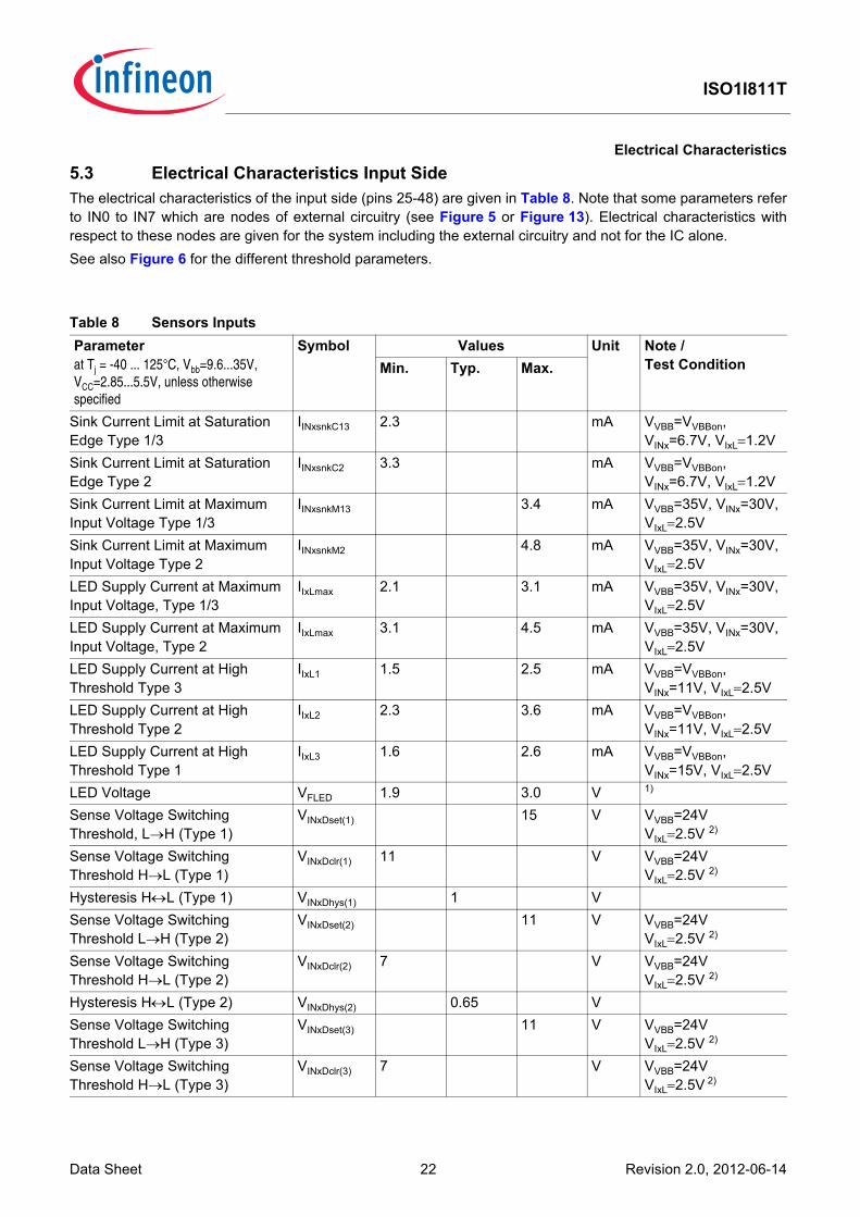
5.3 Electrical Characteristics Input SideThe electrical characteristics of the input side (pins 25-48) are given in Table 8. Note that some parameters referto IN0 to IN7 which are nodes of external circuitry (see Figure 5 or Figure 13). Electrical characteristics withrespect to these nodes are given for the system including the external circuitry and not for the IC alone. See also Figure 6 for the different threshold parameters.
Table 8 Sensors InputsParameterat Tj = -40 ... 125°C, Vbb=9.6...35V, VCC=2.85...5.5V, unless otherwise specified
Symbol Values Unit Note / Test ConditionMin. Typ. Max.
Sink Current Limit at Saturation Edge Type 1/3
IINxsnkC13 2.3 mA VVBB=VVBBon, VINx=6.7V, VIxL=1.2V
Sink Current Limit at Saturation Edge Type 2
IINxsnkC2 3.3 mA VVBB=VVBBon, VINx=6.7V, VIxL=1.2V
Sink Current Limit at Maximum Input Voltage Type 1/3
IINxsnkM13 3.4 mA VVBB=35V, VINx=30V, VIxL=2.5V
Sink Current Limit at Maximum Input Voltage Type 2
IINxsnkM2 4.8 mA VVBB=35V, VINx=30V, VIxL=2.5V
LED Supply Current at Maximum Input Voltage, Type 1/3
IIxLmax 2.1 3.1 mA VVBB=35V, VINx=30V, VIxL=2.5V
LED Supply Current at Maximum Input Voltage, Type 2
IIxLmax 3.1 4.5 mA VVBB=35V, VINx=30V, VIxL=2.5V
LED Supply Current at High Threshold Type 3
IIxL1 1.5 2.5 mA VVBB=VVBBon, VINx=11V, VIxL=2.5V
LED Supply Current at High Threshold Type 2
IIxL2 2.3 3.6 mA VVBB=VVBBon, VINx=11V, VIxL=2.5V
LED Supply Current at High Threshold Type 1
IIxL3 1.6 2.6 mA VVBB=VVBBon, VINx=15V, VIxL=2.5V
LED Voltage VFLED 1.9 3.0 V 1)
Sense Voltage Switching Threshold, L→H (Type 1)
VINxDset(1) 15 V VVBB=24VVIxL=2.5V 2)
Sense Voltage Switching Threshold H→L (Type 1)
VINxDclr(1) 11 V VVBB=24VVIxL=2.5V 2)
Hysteresis H↔L (Type 1) VINxDhys(1) 1 VSense Voltage Switching Threshold L→H (Type 2)
VINxDset(2) 11 V VVBB=24V VIxL=2.5V 2)
Sense Voltage Switching Threshold H→L (Type 2)
VINxDclr(2) 7 V VVBB=24VVIxL=2.5V 2)
Hysteresis H↔L (Type 2) VINxDhys(2) 0.65 VSense Voltage Switching Threshold L→H (Type 3)
VINxDset(3) 11 V VVBB=24VVIxL=2.5V 2)
Sense Voltage Switching Threshold H→L (Type 3)
VINxDclr(3) 7 V VVBB=24VVIxL=2.5V 2)
Data Sheet 22 Revision 2.0, 2012-06-14
ISO1I811T
Electrical Characteristics
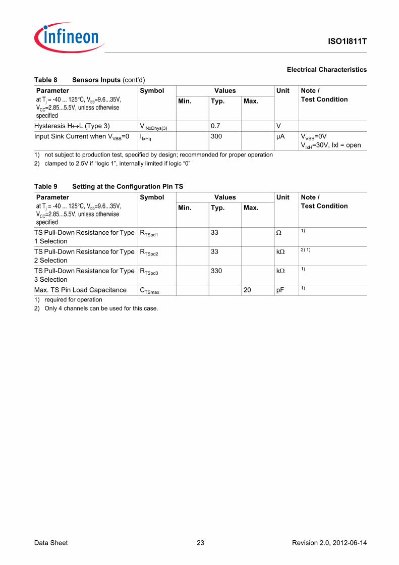
Hysteresis H↔L (Type 3) VINxDhys(3) 0.7 VInput Sink Current when VVBB=0 IIxHq 300 µA VVBB=0V
VIxH=30V, Ixl = open1) not subject to production test, specified by design; recommended for proper operation2) clamped to 2.5V if “logic 1”, internally limited if logic “0”
Table 9 Setting at the Configuration Pin TSParameterat Tj = -40 ... 125°C, Vbb=9.6...35V, VCC=2.85...5.5V, unless otherwise specified
Symbol Values Unit Note / Test ConditionMin. Typ. Max.
TS Pull-Down Resistance for Type 1 Selection
RTSpd1 33 Ω 1)
1) required for operation
TS Pull-Down Resistance for Type 2 Selection
RTSpd2 33 kΩ 2) 1)
2) Only 4 channels can be used for this case.
TS Pull-Down Resistance for Type 3 Selection
RTSpd3 330 kΩ 1)
Max. TS Pin Load Capacitance CTSmax 20 pF 1)
Table 8 Sensors Inputs (cont’d)Parameterat Tj = -40 ... 125°C, Vbb=9.6...35V, VCC=2.85...5.5V, unless otherwise specified
Symbol Values Unit Note / Test ConditionMin. Typ. Max.
Data Sheet 23 Revision 2.0, 2012-06-14
ISO1I811T
Electrical Characteristics
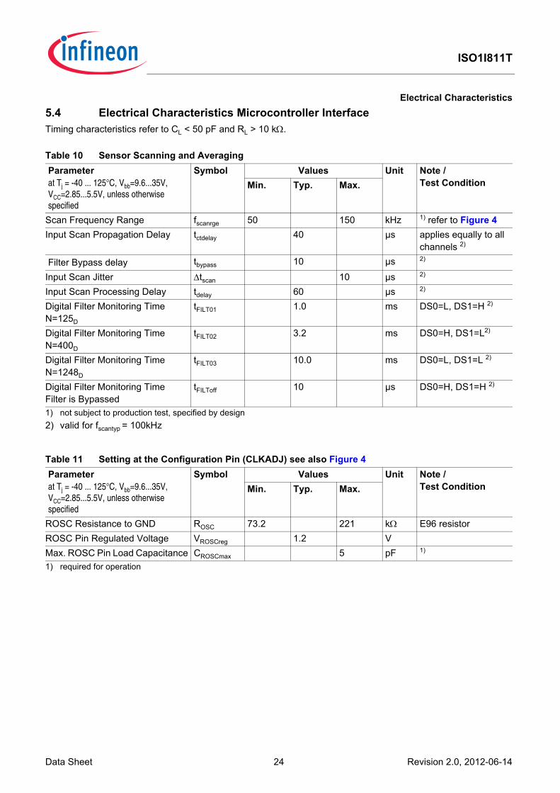
5.4 Electrical Characteristics Microcontroller InterfaceTiming characteristics refer to CL < 50 pF and RL > 10 kΩ.
Table 10 Sensor Scanning and AveragingParameterat Tj = -40 ... 125°C, Vbb=9.6...35V, VCC=2.85...5.5V, unless otherwise specified
Symbol Values Unit Note / Test ConditionMin. Typ. Max.
Scan Frequency Range fscanrge 50 150 kHz 1) refer to Figure 4
1) not subject to production test, specified by design
Input Scan Propagation Delay tctdelay 40 µs applies equally to all channels 2)
2) valid for fscantyp = 100kHz
Filter Bypass delay tbypass 10 µs 2)
Input Scan Jitter Δtscan 10 µs 2)
Input Scan Processing Delay tdelay 60 µs 2)
Digital Filter Monitoring TimeN=125D
tFILT01 1.0 ms DS0=L, DS1=H 2)
Digital Filter Monitoring TimeN=400D
tFILT02 3.2 ms DS0=H, DS1=L2)
Digital Filter Monitoring TimeN=1248D
tFILT03 10.0 ms DS0=L, DS1=L 2)
Digital Filter Monitoring TimeFilter is Bypassed
tFILToff 10 µs DS0=H, DS1=H 2)
Table 11 Setting at the Configuration Pin (CLKADJ) see also Figure 4Parameterat Tj = -40 ... 125°C, Vbb=9.6...35V, VCC=2.85...5.5V, unless otherwise specified
Symbol Values Unit Note / Test ConditionMin. Typ. Max.
ROSC Resistance to GND ROSC 73.2 221 kΩ E96 resistor ROSC Pin Regulated Voltage VROSCreg 1.2 VMax. ROSC Pin Load Capacitance CROSCmax 5 pF 1)
1) required for operation
Data Sheet 24 Revision 2.0, 2012-06-14
ISO1I811T
Electrical Characteristics
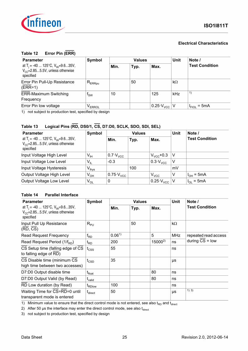
Table 12 Error Pin (ERR)Parameterat Tj = -40 ... 125°C, Vbb=9.6...35V, VCC=2.85...5.5V, unless otherwise specified
Symbol Values Unit Note / Test ConditionMin. Typ. Max.
Error Pin Pull-Up Resistance (ERR=1)
RERRpu 50 kΩ
ERR-Maximum Switching Frequency
fSW 10 125 kHz 1)
1) not subject to production test, specified by designError Pin low voltage VERROL 0.25·VVCC V IFIOL = 5mA
Table 13 Logical Pins (RD, DS0/1, CS, D7:D0, SCLK, SDO, SDI, SEL)Parameterat Tj = -40 ... 125°C, Vbb=9.6...35V, VCC=2.85...5.5V, unless otherwise specified
Symbol Values Unit Note / Test ConditionMin. Typ. Max.
Input Voltage High Level VIH 0.7·VVCC VVCC+0.3 VInput Voltage Low Level VIL -0.3 0.3·VVCC VInput Voltage Hysteresis VIhys 100 mVOutput Voltage High Level VOH 0.75·VVCC VVCC V IOH = 5mAOutput Voltage Low Level VOL 0 0.25·VVCC V IOL = 5mA
Table 14 Parallel Interface Parameterat Tj = -40 ... 125°C, Vbb=9.6...35V, VCC=2.85...5.5V, unless otherwise specified
Symbol Values Unit Note / Test ConditionMin. Typ. Max.
Input Pull Up Resistance(RD, CS)
RPU 50 kΩ
Read Request Frequency fRD 0.061)
1) Minimum value to ensure that the direct control mode is not entered, see also tRD and tdirect
5 MHz repeated read access during CS = lowRead Request Period (1/fRD) tRD 200 150002)
2) After 50 µs the interface may enter the direct control mode, see also tdirect
ns CS Setup time (falling edge of CS to falling edge of RD)
tCSS 55 ns
CS Disable time (minimum CS high time between two accesses)
tCSD 35 µs
D7:D0 Output disable time tfloat 80 nsD7:D0 Output Valid (by Read) tvalid 80 nsRD Low duration (by Read) tRDlow 100 nsWaiting Time for CS=RD=0 until transparent mode is entered
tdirect 50 µs 1) 3)
3) not subject to production test, specified by design
Data Sheet 25 Revision 2.0, 2012-06-14
ISO1I811T
Electrical Characteristics
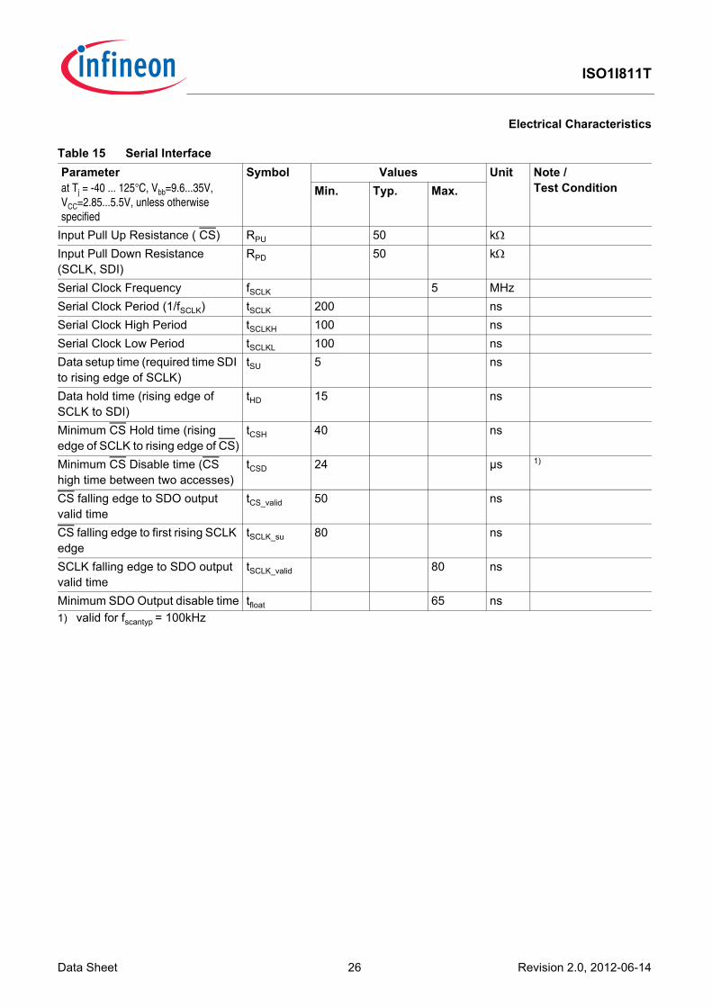
Table 15 Serial Interface Parameterat Tj = -40 ... 125°C, Vbb=9.6...35V, VCC=2.85...5.5V, unless otherwise specified
Symbol Values Unit Note / Test ConditionMin. Typ. Max.
Input Pull Up Resistance ( CS) RPU 50 kΩInput Pull Down Resistance (SCLK, SDI)
RPD 50 kΩ
Serial Clock Frequency fSCLK 5 MHzSerial Clock Period (1/fSCLK) tSCLK 200 ns Serial Clock High Period tSCLKH 100 ns Serial Clock Low Period tSCLKL 100 ns Data setup time (required time SDI to rising edge of SCLK)
tSU 5 ns
Data hold time (rising edge of SCLK to SDI)
tHD 15 ns
Minimum CS Hold time (rising edge of SCLK to rising edge of CS)
tCSH 40 ns
Minimum CS Disable time (CS high time between two accesses)
tCSD 24 µs 1)
1) valid for fscantyp = 100kHz
CS falling edge to SDO output valid time
tCS_valid 50 ns
CS falling edge to first rising SCLK edge
tSCLK_su 80 ns
SCLK falling edge to SDO output valid time
tSCLK_valid 80 ns
Minimum SDO Output disable time tfloat 65 ns
Data Sheet 26 Revision 2.0, 2012-06-14
Data Sheet 27 Revision 2.0, 2012-06-14 ,
ISO1I811T
Package Outline
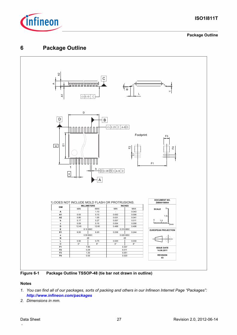
6 Package Outline
Figure 6-1 Package Outline TSSOP-48 (tie bar not drawn in outline)
Notes1. You can find all of our packages, sorts of packing and others in our Infineon Internet Page “Packages”:
http://www.infineon.com/packages2. Dimensions in mm.
0.496
0.043
0.011
0.006
0.244
0.030
MILLIMETERS
L
D
b
DIM
A1
A
c
E
E1
N
-
MIN
0.020
MAX
INCHES
0.488
MIN
-
0.002
0.007
0.004
0.236
MAX SCALE
1.00
2mm
0
1.00.05
1.10
0.17 0.27
0.16
12.60
6.206.00
12.40
0.09
0.750.50
1) DOES NOT INCLUDE MOLD FLASH OR PROTRUSIONS.
03
ISSUE DATE
14.06.2011
DOCUMENT NO.
Z8B00158954
EUROPEAN PROJECTION
REVISION
A
A2
A1
b
e
D
E E1
L
c
0.15 0.006
A2 0.0310.80 1.05 0.041
8.10 BSC 0.319 BSC
e 0.50 BSC 0.020 BSC
48 48
1
O
8°0° 8°0°Θ
F1 0.3077.80
F2 0.0110.29
F3 0.0511.30
F4 0.0200.50
F1
F3
F2
F4
Footprint
A
B
D
C