Embed Size (px)
Citation preview
3-61
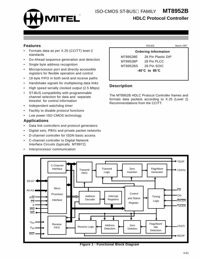
Features• Formats data as per X.25 (CCITT) level-2
standards
• Go-Ahead sequence generation and detection
• Single byte address recognition
• Microprocessor port and directly accessibleregisters for flexible operation and control
• 19 byte FIFO in both send and receive paths
• Handshake signals for multiplexing data links
• High speed serially clocked output (2.5 Mbps)
• ST-BUS compatibility with programmablechannel selection for data and separatetimeslot for control information
• Independent watchdog timer
• Facility to disable protocol functions
• Low power ISO-CMOS technology
Applications• Data link controllers and protocol generators
• Digital sets, PBXs and private packet networks
• D-channel controller for ISDN basic access
• C-channel controller to Digital NetworkInterface Circuits (typically MT8972)
• Interprocessor communication
Description
The MT8952B HDLC Protocol Controller frames andformats data packets according to X.25 (Level 2)Recommendations from the CCITT.
Ordering Information
MT8952BE 28 Pin Plastic DIPMT8952BP 28 Pin PLCCMT8952BS 28 Pin SOIC
-40°C to 85 °C
Figure 1 - Functional Block Diagram
D0-D7
A0-A3
R/W
CSE
IRQWD
VDD
VSS
RST
TEOP
CDSTo
F0i
CKi
RxCEN
TxCEN
CDSTi
REOP
C-ChannelInterface
Micro
Processor
Interface
ReceiveFIFO
TransmitFIFO
TransmitLogic
ZeroInsertion
Flag/AbortGenerator
AddressDecoder
InterruptRegisters
Control
and Status
Register
Timing
Logic
Receive Logic AddressDetection
ZeroDeletion
Flag/Abort/Idle
Detection
ISSUE6 March 1997
MT8952BHDLC Protocol Controller
ISO-CMOS ST-BUS FAMILY

MT8952B ISO-CMOS
3-62
Figure 2 - Pin Connections
Pin Description
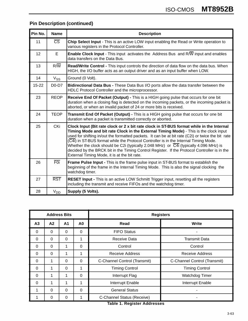
Pin No. Name Description
1 TxCEN Transmit Clock Enable - This active LOW input enables the transmit section in the ExternalTiming Mode. When LOW, CDSTo is enabled and when HIGH, CDSTo is in high impedancestate. If the Protocol Controller is in the Internal Timing Mode, this input is ignored.
2 RxCEN Receive Clock Enable - This active LOW input enables the receive section in the ExternalTiming Mode. When LOW, CDSTi is enabled and when HIGH, the clock to the receivesection is inhibited. If the Protocol Controller is in the Internal Timing Mode, this input isignored.
3 CDSTo C and D channel Output in ST-BUS format - This is the serial formatted data output fromthe transmitter in NRZ form. It is in ST-BUS format if the Protocol Controller is in InternalTiming Mode with the data in selected timeslots (0,2,3 and 4) and the C-channel informationin timeslot No. 1. If the Protocol Controller is in External Timing Mode, the formatted data isoutput on the rising edge of the clock (CKi) when TxCEN LOW. If TxCEN is HIGH, CDSTo isin high impedance state.
4 CDSTi C and D channel Input in ST-BUS format - This is the serial formatted data input to thereceiver in NRZ form. It must be in ST-BUS format if the Protocol Controller is in InternalTiming Mode with the input data in selected timeslots (0,2,3 and 4) and the C-channelinformation in timeslot No.1. If the Controller is in External Timing Mode, the serial inputdata is sampled on the falling edge of the clock CKi when RxCEN is LOW. If RxCEN isHIGH, the clock to receive section is inhibited.
5 WD Watch-Dog Timer output - Normally a HIGH level output, going LOW if the Watchdog timertimes out or if the external reset (RST) is held LOW. The WD output remains LOW as longas RST is held LOW.
6 IRQ Interrupt Request Output (Open Drain) - This active LOW output notifies the controllingmicroprocessor of an interrupt request. It goes LOW only when the bits in the InterruptEnable Register are programmed to acknowledge the source of the interrupt as defined inthe Interrupt Flag Register.
7-10 A0-A3 Address Bus Inputs - These bits address the various registers in the Protocol Controller.They select the internal registers in conjunction with CS, R/W inputs and E Clock. (Refer toTable 1.)
28 PIN PLCC
TxCENRxCENCDSToCDSTi
WDIRQA0A1A2A3CS
ER/WVSS
VDDRSTF0iCKiTEOPREOPD7D6D5D4D3D2D1D0
28 PIN PDIP/SOIC
123456789
1011121314 15
1617181920
2827262524232221
4
567891011
25242322212019
•
CD
ST
i
CKiTEOPREOPD7D6D5D4
WDIRQA0A1A2A3CS
D2
3 2 1 28 27 26
12 13 14 15 16 17 18
CD
ST
oR
xCE
NT
xCE
NV
DD
RS
TF
0i
ER
/WV
SS
D0
D1
D3
ISO-CMOS MT8952B
3-63
Table 1. Register Addresses
11 CS Chip Select Input - This is an active LOW input enabling the Read or Write operation tovarious registers in the Protocol Controller.
12 E Enable Clock Input - This input activates the Address Bus and R/W input and enablesdata transfers on the Data Bus.
13 R/W Read/Write Control - This input controls the direction of data flow on the data bus. WhenHIGH, the I/O buffer acts as an output driver and as an input buffer when LOW.
14 VSS Ground (0 Volt).
15-22 D0-D7 Bidirectional Data Bus - These Data Bus I/O ports allow the data transfer between theHDLC Protocol Controller and the microprocessor.
23 REOP Receive End Of Packet (Output) - This is a HIGH going pulse that occurs for one bitduration when a closing flag is detected on the incoming packets, or the incoming packet isaborted, or when an invalid packet of 24 or more bits is received.
24 TEOP Transmit End Of Packet (Output) - This is a HIGH going pulse that occurs for one bitduration when a packet is transmitted correctly or aborted.
25 CKi Clock Input (Bit rate clock or 2 x bit rate clock in ST-BUS format while in the InternalTiming Mode and bit rate Clock in the External Timing Mode) - This is the clock inputused for shifting in/out the formatted packets. It can be at bit rate (C2i) or twice the bit rate(C4i) in ST-BUS format while the Protocol Controller is in the Internal Timing Mode.Whether the clock should be C2i (typically 2.048 MHz) or C4i (typically 4.096 MHz) isdecided by the BRCK bit in the Timing Control Register. If the Protocol Controller is in theExternal Timing Mode, it is at the bit rate.
26 F0i Frame Pulse Input - This is the frame pulse input in ST-BUS format to establish thebeginning of the frame in the Internal Timing Mode. This is also the signal clocking thewatchdog timer.
27 RST RESET Input - This is an active LOW Schmitt Trigger input, resetting all the registersincluding the transmit and receive FIFOs and the watchdog timer.
28 VDD Supply (5 Volts).
Address Bits Registers
A3 A2 A1 A0 Read Write
0 0 0 0 FIFO Status -
0 0 0 1 Receive Data Transmit Data
0 0 1 0 Control Control
0 0 1 1 Receive Address Receive Address
0 1 0 0 C-Channel Control (Transmit) C-Channel Control (Transmit)
0 1 0 1 Timing Control Timing Control
0 1 1 0 Interrupt Flag Watchdog Timer
0 1 1 1 Interrupt Enable Interrupt Enable
1 0 0 0 General Status -
1 0 0 1 C-Channel Status (Receive) -
Pin Description (continued)
Pin No. Name Description
MT8952B ISO-CMOS
3-64
Introduction
The MT8952B HDLC Protocol Controller handles bitoriented protocol structure and formats the data asper the packet switching protocol defined in the X.25(Level 2) recommendations of the CCITT. Ittransmits and receives the packeted data(information or control) serially in a format shown inFigure 3 , while providing the data transparency byzero insertion and deletion. It generates and detectsthe flags, various link channel states and the abortsequence. Further, it provides a cyclic redundancycheck on the data packets using the CCITT definedpolynomial. In addition, it can generate and detect aGo Ahead sequence and recognize a single byteaddress in the received frame. There is also aprovision to disable the protocol functions andprovide transparent access to the serial bus throughthe parallel port.
Frame Format
All frames start with an opening flag and end with aclosing flag as shown in Figure 3. Between thesetwo flags, a frame contains the data and the framecheck sequence (FCS).
Figure 3. Frame Format
Flag:
The flag is a unique pattern of 8 bits (01111110)defining the frame boundary. The transmit sectiongenerates the flags and appends them automaticallyto the frame to be transmitted. The receive sectionsearches the incoming packets for flags on a bit-by-bit basis and establishes frame synchronization. Theflags are used only to identify and synchronize thereceived frame and are not transferred to the FIFO.
Data:
The data field refers to the Address, Control andInformation fields defined in the CCITTrecommendations. A valid frame should have a datafield of at least 16 bits. The first byte in the data fieldis the address of the frame. If RxAD bit in theControl Register is HIGH, the incoming packet isrecognized only if the address byte matches the bytestored in the Receive Address Register or theaddress byte is the All-Call Address (all ONEs). TheLSB of the Receive Address Register is set LOWpermanently and the comparison is done only onupper seven bits of the received address byte. The
address detection can be limited only to the uppersix bits by setting HIGH both RA6/7 and RxAD bits inthe Control Register.
Frame Check Sequence (FCS):
The 16 bits following the data field are the framecheck sequence bits. The generator polynomial is:
G(x)=x16+x12+x5+1The transmitter calculates the FCS on all bits of thedata field and transmits after the data field andbefore the end flag. The receiver performs a similarcomputation on all bits of the received data and FCSfields and the result is compared with FOB8Hex. If itmatches, the received data is assumed error free.The error status of the received packet is indicatedby D7 and D6 bits in the FIFO Status Register.
Zero Insertion and Deletion:
The Protocol Controller, while sending either datafrom the FIFO or the 16 bits FCS, checks thetransmission on a bit-by-bit basis and inserts aZERO after every sequence of five contiguous ONEs(including the last five bits of FCS) to ensure that theflag sequence is not simulated. Similarly thereceiver examines the incoming frame content anddiscards any ZERO directly following the fivecontiguous ONEs.
Abort:
The transmitter aborts a frame by sending eightconsecutive ONEs. The FA bit in the ControlRegister along with a write operation to the TransmitData Register enables the transmission of abortsequence instead of the byte written to the register.On the receive side, the ABRT bit in the GeneralStatus Register is set whenever an abort sequence(7 or more continuous 1’s) is received. The abortsequence causes the receiver to abandon whateverit was doing and start searching for a start flag. TheFA bit in the Interrupt Status Register is set when anabort sequence is received following a start flag andat least four data bytes (minimum for a valid frame).
Interframe Time Fill and Link ChannelStates
When the HDLC Protocol Controller is not sendingpackets, the transmitter can be in any of three statesmentioned below depending on the status of theIFTF0 and IFTF1 bits in the Control Register. Thesebits are also used to disable the protocol function toprovide the transparent parallel access to the serialbus through the microprocessor port.
FLAG DATA FIELD FCS FLAG
OneByte
n Bytes (n ≥ 2)
TwoBytes
OneByte
ISO-CMOS MT8952B
3-65
Idle state:
The Idle state is defined as 15 or more contiguousONEs. When the HDLC Protocol Controller isobserving this condition on the receiving channel,the Idle bit in the General Status Register is setHIGH. On the transmit side, the Protocol Controllerends the Idle state when data is loaded into thetransmit FIFO.
Interframe time fill state:
The Protocol Controller transmits continuous flags(7EHex) in Interframe time fill state and ends thisstate when data is loaded into the transmit FIFO.
Go Ahead state:
Go Ahead is defined by the 9 bit sequence011111110 (7FHex followed by a ZERO), and hencecontiguous 7F’s appear as Go Aheads. Once thetransmitter is in ‘Go Ahead’ state, it will continue toremain so even after the data is loaded into theFIFO. This state can only be changed by setting theIFTF bits in the Control Register to something otherthan ‘GO Ahead’. The reception of this sequence isindicated by GA bit in the General Status Registerand the Protocol Controller can generate an interruptif enabled to do so by the GA bit in the InterruptEnable Register.
Transparent Data Transfer State:
The Protocol Controller, in this state, disables theprotocol functions defined earlier and provides bi-directional access to the serial bit streams throughthe parallel port. Like other states, the transparentdata transfer can be selected in both timing modes.
Invalid Frames
Any frame shorter than 32 bits between the openingand closing flags (corresponding to 16 bits of dataand 16 bits FCS) is considered invalid. The ProtocolController ignores the frame only if the frame lengthis less than 24 bits between the flags. For frames oflength 24 to 32 bits, it transfers the data field to FIFOand tags it as having bad FCS in the FIFO StatusRegister.
Functional Description
The functional block diagram of the HDLC ProtocolController is shown in Figure 1. It has two ports.The serial port transmits and receives formatted datapackets and the parallel port provides amicroprocessor interface for access to variousregisters in the Protocol Controller.
The serial port can be configured to operate in twomodes depending on the IC bit in the Timing ControlRegister. It can transmit/receive the packets onselected timeslots in ST- BUS format or it can,using the enable signals (TxCEN and RxCEN),transmit/receive the packets at a bit rate equal to CKiclock input.
The microprocessor port allows parallel datatransfers between the Protocol Controller and a6800/6809 system bus. This interface consists ofData Bus (D0-D7), Address Bus (A0-A3), E Clock,Chip Select (CS) and R/W control. The micro-processor can read and write to the various registersin the Protocol Controller. The addresses of theseregisters are given in Table 2. The IRQ is an opendrain, active LOW output indicating an interruptrequest to CPU. Control and monitoring of manydifferent interrupts that may originate from theprotocol controller is implemented by the InterruptFlag Register (IFR) and the Interrupt EnableRegister (IER). Specific events have been describedthat set a bit HIGH in the Interrupt Flag Register.Such an event does not necessarily interrupt theCPU. To assert an interrupt (pull IRQ output LOW)the bit in IER that coincides with the Interrupt FlagRegister must be set HIGH. The IRQ bit in theGeneral Status Register is the complement of IRQpin status. If an interrupt is asserted, this bit will beset HIGH otherwise it will be LOW.
TEOP and REOP Outputs:
The HDLC Protocol Controller provides two separatesignals TEOP & REOP indicating the end of packettransmitted and received respectively. TEOP is aHIGH going pulse for one bit duration assertedduring the last bit of the closing flag or Abortsequence of the transmit packet. REOP is also aHIGH going pulse occurring for one bit period whena closing flag is received or an incoming packet isaborted or an invalid packet of 24 or more bits isdetected. However, REOP is not generated forinvalid packets of length less than 24 bits. These‘end of packet’ signals are useful in multiplexingseveral data links on to a single HDLC ProtocolController.
Timing Modes
There are two timing modes the Protocol Controllercan be run in. These timing modes refer only to theconfiguration of the serial port and are not related tothe microprocessor port.
Internal Timing Mode
The Internal Timing Mode is intended for an easyinterface to various products using ST-BUS

MT8952B ISO-CMOS
3-66
architecture, particularly MITEL’s Digital NetworkInterface Circuit (DNIC - MT8972). The data/packetsare shifted in/out serially in ST-BUS format using thetiming signals F0i and C2i/C4i. In addition to framingthe data, the Protocol Controller reserves onechannel (channel-1) on the ST-BUS for carryingcontrol information (C-channel) and this timeslot cannot be used for the packetized data. While theProtocol Controller is in the Internal Timing Mode,the clock input CKi can be either at the bit rate or at2°bit rate depending on the BRCK bit in the TimingControl Register as shown in Table 2.
Table 2. Output Bit Rate In Internal Timing Mode
The Protocol Controller uses the ST-BUS timingsignals F0i and C2i/C4i, and enables the transmitterand receiver sections in the appropriate timeslotsas determined by TC0-TC3 bits in the TimingControl Register.
The TxCEN and RxCEN inputs are ignored in thismode.
C-Channel Interface
This is a separate control channel (C-channel)interface relevant only in the Internal Timing Mode.The data stored in the C-Channel Control Register isshifted out during the channel-1 timeslot of theoutgoing ST-BUS (CDSTo) and the C1EN bit in theTiming Control Register enables the transmission.The transmission of C-Channel is independent ofpacket/data transmission. The data received onchannel-1 of the incoming ST-BUS (CDSTi) is shiftedinto the C-Channel Status Register independentlyand it is updated continuously.
Both the C-channel registers are accessible by theaccompanying CPU through the parallel port.
External Timing Mode
In the External Timing Mode, the transmit andreceive sections are enabled independently byTxCEN and RxCEN control inputs and the formatteddata packets are shifted in/out serially at a rate equalto the clock frequency on CKi. The output istransmitted on the rising edge and the receiversamples the input on the falling edge of the clock.The TxCEN and RxCEN controls are independent
and asynchronous and have effect only after thecurrent bit in the packet is transmitted/received.
Although the protocol controller provides thepacketized data on a limited number of channels onthe ST-BUS while operating in the Internal TimingMode, it can packetize the data on any or all thechannels of the ST-BUS if it is operated in theExternal Timing Mode with appropriate enablesignals on TxCEN and RxCEN.
Transparent Data Transfer
By setting the IFTF bits in the Control Registerappropriately, the protocol functions can be disabled.This provides a bidirectional access to the serial portthrough the microprocessor interface, with 19 bytedeep FIFO in each direction. The transparent datatransfer facility functions in bytewide format and isavailable in both timing modes except when thetiming control bits are set for one bit/frame during theInternal Timing Mode.
The transmit data is shifted out serially on CDSToand the operation being bytewide, only the leastsignificant bits of each byte loaded are transmitted, ifthe timing control bits are set to select 2, 6 or 7 bits/frame. When the transmit FIFO is empty, the lastbyte or the portion the last byte, written to the FIFOis transmitted repeatedly. Similarly the serial data onCDSTi is shifted in and converted to bytewideformat. In case the timeslot selected is 2, 6 or 7 bits/frame, the reception involves only the mostsignificant bits of each byte.
It should be noted that none of the protocol relatedstatus or interrupt bits are applicable in transparentdata transfer state. However, the FIFO related statusand interrupt bits are pertinent and carry the samemeaning as they do while performing the protocolfunctions.
Watchdog Timer
This is a fixed eleven stage binary counter with F0ias the input and WD as the output from the laststage. This counter can be reset either by theexternal input (RST) or by writing XXX0 1010 to theWatchdog Timer Register. The WD output isnormally HIGH and if the Watchdog Timer Registeris not written within 210 cycles of F0i input after it isreset, the WD output will go LOW for a period of 210
cycles of F0i. Even though the F0i input is notrequired for formatting data in the External TimingMode, it is necessary for the operation of thewatchdog timer.
BRCK Bit CKi Input Output DataRate
0 4.096 MHz/C4i 2.048 Mbps
1 2.048 MHz/C2i 2.048 Mbps
ISO-CMOS MT8952B
3-67
Order of Bit Transmission/Reception
The Least Significant Bit (LSB) corresponding to D0on the data bus is transmitted first on the serialoutput (CDSTo). On the receiving side, the first bitreceived on the serial input (CDSTi) is considered asthe LSB and placed on D0 of the data bus.
Registers
There are several registers in the HDLC ProtocolController accessible to the associated micro-processor via the data bus. The addresses of theseregisters are given in Table 1 and their functionaldetails are given below.
FIFO Status Register (Read):
This register (Figure 4) indicates the status oftransmit and receive FIFOs and the received byte asdescribed below.
Figure 4 - FIFO Status Register
Rx Byte Status: These two bits (D7 and D6) indicatethe status of the received byte ready to be read fromthe receive FIFO. The status is encoded as shown inTable 3.
Table 3. Received Byte Status
Rx FIFO Status: These bits (D5 and D4) indicate thestatus of receive FIFO as given by Table 4. The RxFIFO status bits are not updated immediately afteran access of the Rx FIFO (a read from themicroprocessor port, or a write from the serial port),to avoid the existence of unrecoverable errorconditions.
When in external timing mode, the MT8952B mustreceive two falling edges of the clock signal at theCKi input before the Rx FIFO status bits will beupdated. When in internal 2.048 MHz timing mode,the MT8952B must receive two falling edges of theC2i clock before the Rx FIFO status bits will be
Table 4. Receive FIFO Status
updated. When in internal 4.096 MHz timing mode,the MT8952B must receive four falling edges of theC4i clock before the Rx FIFO status bit will beupdated (see the section on Receive Operation -Normal Packets).
Tx FIFO Status: These two bits (D3 and D2) indicatethe status of transmit FIFO as shown in Table 5.
Table 5. Transmit FIFO Status
The Tx FIFO status bits are updated in the samemanner as the Rx FIFO bits, except that in externaltiming mode, and in internal 2.048 Mbps timingmode, the Tx FIFO status bits are updated after twofalling edges of the CKi or the C2i signal (see thesection on Transmit Operation - Normal Packets).
Receive Data Register (Read):
Reading the Receive Data Register (Figure 5) putsthe first byte from the receive FIFO on the data bus.The first bit of the data received on the serial input(CDSTi) is considered to be the LSB and is availableon D0 of the data bus.
Figure 5 - Receive Data Register
Transmit Data Register (Write):
Writing to Transmit Data Register (Figure 6) puts thedata present on the data bus into the transmit FIFO.The LSB (D0) is transmitted first.
D7 D6 D5 D4 D3 D2 D1 D0
Rx ByteStatus
Rx FIFOStatus
Tx FIFOStatus
LOW LOW
Rx ByteStatus Bits StatusD7 D6
0 0 Packet Byte
0 1 First Byte
1 0 Last Byte (Good FCS)
1 1 Last Byte (Bad FCS)
Rx FIFOStatus Bits StatusD5 D4
0 0 Rx FIFO Empty
0 1 Less than or equal to 14 bytes
1 0 Rx FIFO Full
1 1 Greater than or equal to 15 bytes
Tx FIFOStatus Bits StatusD3 D2
0 0 Tx FIFO Full
0 1 Greater than or equal to 5 bytes
1 0 Tx FIFO Empty
1 1 Less than or equal to 4 bytes
D7 D6 D5 D4 D3 D2 D1 D0
RD7 RD6 RD5 RD4 RD3 RD2 RD1 RD0
MT8952B ISO-CMOS
3-68
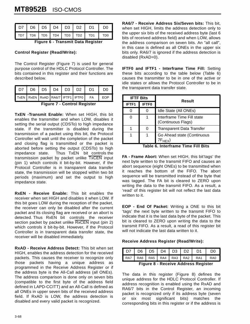
Figure 6 - Transmit Data Register
Control Register (Read/Write):
The Control Register (Figure 7) is used for generalpurpose control of the HDLC Protocol Controller. Thebits contained in this register and their functions aredescribed below.
Figure 7 - Control Register
TxEN -Transmit Enable: When set HIGH, this bitenables the transmitter and when LOW, disables itsetting the serial output (CDSTo) to high impedancestate. If the transmitter is disabled during thetransmission of a packet using this bit, the ProtocolController will wait until the completion of the packetand closing flag is transmitted or the packet isaborted before setting the output (CDSTo) to highimpedance state. Thus TxEN bit controls thetransmission packet by packet unlike TxCEN input(pin 1) which controls it bit-by-bit. However, if theProtocol Controller is in transparent data transferstate, the transmission will be stopped within two bitperiods (maximum) and set the output to highimpedance state.
RxEN - Receive Enable: This bit enables thereceiver when set HIGH and disables it when LOW. Ifthis bit goes LOW during the reception of the packet,the receiver can only be disabled after the currentpacket and its closing flag are received or an abort isdetected. Thus RxEN bit controls the receiversection packet by packet unlike RxCEN input (pin 2)which controls it bit-by-bit. However, if the ProtocolController is in transparent data transfer state, thereceiver will be disabled immediately.
RxAD - Receive Address Detect: This bit when setHIGH, enables the address detection for the receivedpackets. This causes the receiver to recognize onlythose packets having a unique address asprogrammed in the Receive Address Register or ifthe address byte is the All-Call address (all ONEs).The address comparison is done only on seven bits(compatible to the first byte of the address fielddefined in LAPD-CCITT) and an All-Call is defined asall ONEs in upper seven bits of the received addressfield. If RxAD is LOW, the address detection isdisabled and every valid packet is recognized.
RA6/7 - Receive Address Six/Seven bits: This bit,when set HIGH, limits the address detection only tothe upper six bits of the received address byte (last 6bits of received address field) and when LOW, allowsthe address comparison on seven bits. An "all call",in this case is defined as all ONEs in the upper sixbits only. RA6/7 is ignored if the address detection isdisabled (RxAD=0).
IFTF0 and IFTF1 - Interframe Time Fill: Settingthese bits according to the table below (Table 6)causes the transmitter to be in one of the active oridle states or allows the Protocol Controller to be inthe transparent data transfer state.
Table 6. Interframe Time Fill Bits
FA - Frame Abort: When set HIGH, this bit’tags’ thenext byte written to the transmit FIFO and causes anabort sequence (eight ONEs) to be transmitted whenit reaches the bottom of the FIFO. The abortsequence will be transmitted instead of the byte thatwas tagged. The FA bit is cleared to ZERO uponwriting the data to the transmit FIFO. As a result, a‘read’ of this register bit will not reflect the last datawritten to it.
EOP - End Of Packet: Writing a ONE to this bit‘tags’ the next byte written to the transmit FIFO toindicate that it is the last data byte of the packet. Thisbit is cleared to ZERO upon writing the data to thetransmit FIFO. As a result, a read of this register bitwill not indicate the last data written to it.
Receive Address Register (Read/Write):
Figure 8 - Receive Address Register
The data in this register (Figure 8) defines theunique address for the HDLC Protocol Controller. Ifaddress recognition is enabled using the RxAD andRA6/7 bits in the Control Register, an incomingpacket is recognized only if its address byte (sevenor six most significant bits) matches thecorresponding bits in this register or if the address is
D7 D6 D5 D4 D3 D2 D1 D0
TD7 TD6 TD5 TD4 TD3 TD2 TD1 TD0
D7 D6 D5 D4 D3 D2 D1 D0
TxEN RxEN RxAD RA6/7 IFTF1 IFTF0 FA EOP IFTF BitsResult
IFTF1 IFTF0
0 0 Idle State (All ONEs)
0 1 Interframe Time Fill state(Continuous Flags)
1 0 Transparent Data Transfer
1 1 Go Ahead state (Continuous7FHEX)
D7 D6 D5 D4 D3 D2 D1 D0
RA7 RA6 RA5 RA4 RA3 RA2 RA1 RA0

ISO-CMOS MT8952B
3-69
an "all-call". The LSB of the Receiver AddressRegister is set LOW permanently and the addresscomparison is done only on remaining bits of theregister.
C-Channel Control Register (Read/Write):
Figure 9 - C-Channel Control Register
The data written to this register (Figure 9) istransmitted on channel-1 slot of the outgoing ST-BUS (CDSTo), when enabled by C1EN bit in theTiming Control Register. This feature can only beused when the HDLC Protocol Controller is in theInternal Timing Mode.
Timing Control Register (Read/Write):
The Timing Control Register (Figure 10) controls thetiming mode and other related operations andprovides a software reset to the Protocol Controller.The various bits in this register are described below:
Figure 10. Timing Control Register
RST - Reset: When this bit is set HIGH, all theregisters in the HDLC Protocol Controller are resetand the data in the FIFOs is lost. This is equivalent tothe external reset with the exception that the RST bitdoes not affect itself or the Watchdog Timer Registerand WD output. The RST bit must be “cleared”(written as a logic “0”) twice before the MT8952B willbe removed from its reset state (see section onRESET operation).
IC - Internal Control: When this bit is cleared toZERO, the Protocol Controller is in the ExternalTiming Mode. The transmit and receive sections areenabled by the inputs TxCEN and RxCENrespectively, and F0i is used only for the watchdogtimer operation. When this bit is a ONE, the ProtocolController is in the Internal Timing Mode. Thetransmit and receive sections are enabled by theinternally generated timings derived from the inputsCKi and F0i. The F0i input defines the beginning of aframe (Figure 24) and the transmitter and receiversections are enabled in the timeslots as determinedby the bits TCO-TC3. The inputs TxCEN and RxCENare ignored in this mode.
C1EN - Channel-1 Enable: When HIGH, it enablesthe transmission of C-channel information onchannel-1 time-slot of the outgoing ST-BUS (CDSTo)and when LOW, puts CDSTo into high impedance
state during that period. However, the C-channelinformation is received independently and the C-channel Status Register is updated continuously.Note that C1EN has relevance only during theInternal Timing Mode.
BRCK- Bit Rate Clock: This bit is used during theInternal Timing Mode to select the clock rate andignored if the Protocol Controller is in the ExternalTiming Mode. It should be set HIGH if the input clock(CKi) is at the bit rate (C2i) and should be LOW forthe clock input at 2 x bit rate (C4i). In both cases,the clock should be properly phase related to F0i asshown in Figure 25.
TC0-TC3 - Timing Control Bits: In the InternalTiming Mode the transmitter and the receiversections are enabled during the times defined by theTiming Control Bits TC0-TC3 (Table 7). This appliesonly to the ST-BUS channels 0, 2, 3 and 4 carryingthe packets or transparent data (channel-1 pertainsto C-channel information). The output CDSTo is putduring the remaining time intervals not enabled bythese bits.
X : Don’t Care Table 7. Timing Control Bits
Interrupt Flag Register (Read):
Reading the Interrupt Flag Register puts the interruptstatus bits on the data bus. This register is resetwhen it is read and a particular bit will not be set untilits particular condition occurs again. The functionaldetails of each bit are provided in Figure 11.
Figure 11. Interrupt Flag Register
GA - Go Ahead: This bit when set HIGH, indicatesthe detection of ‘go ahead’ sequence on theincoming data stream (CDSTi).
D7 D6 D5 D4 D3 D2 D1 D0
CT7 CT6 CT5 CT4 CT3 CT2 CT1 CT0
D7 D6 D5 D4 D3 D2 D1 D0
RST IC C1EN BRCK TC3 TC2 TC1 TC0Timing Control Bits ST-BUS
ChannelNumber
Bits/FrameTC3 TC2 TC1 TC0
X 0 0 0 0 1X 0 0 1 0 20 0 1 0 0 61 0 1 0 0 7X 0 1 1 2 8X 1 0 0 3 8X 1 0 1 4 8X 1 1 0 2 and 3 16X 1 1 1 2, 3 and 4 24
D7 D6 D5 D4 D3 D2 D1 D0GA EOPD Tx
DONEFA Tx
4/19FULL
TxURUN
Rx15/19FULL
RxOFLW

MT8952B ISO-CMOS
3-70
EOPD - End of Packet Detect: A HIGH on this bitconfirms the reception of an ‘end of packet’ flag, anabort sequence or an invalid packet of 24 or morebits on the incoming data stream (CDSTi).
Tx DONE - Transmitter Done: This bit, when HIGH,indicates that the packet transmission is completeand the Transmit FIFO is empty. The falling edge ofTEOP output causes this interrupt status bit to be setHIGH if the FIFO is empty.
FA - Frame Abort: This bit is set HIGH to indicatethat a frame abort has been detected on theincoming data stream.
Tx 4/19 FULL - Transmit FIFO 4/19 full: This bit ifset HIGH, indicates that the transmit FIFO has only 4bytes remaining in it and another 15 bytes could beloaded. This bit has significance only when thetransmit FIFO is being depleted and not when it isgetting loaded.
Tx URUN - Transmit FIFO underrun: This bit whenHIGH, identifies that the transmit FIFO is emptywithout the Protocol Controller being given the ‘endof packet’ indication. This indicates that the transmitFIFO has underrun and the Protocol Controller willtransmit an abort sequence automatically. Tx DONEwill be set 8 bit times after Tx URUN is set.
Rx15/19 FULL - Receive FIFO 15/19 full: This bitwhen HIGH, confirms that the receive FIFO has 15bytes in it and it can receive four more bytes.
Rx OFLW - Receive FIFO overflow: This bit whenset HIGH, indicates that the receive FIFO is full anda ‘write’ occurred indicating an overflow. The bytecausing this and all the subsequent bytes writtenwhile the FIFO is in this state are lost. The receiverbegins to search for a new start flag.
Watchdog Timer Register (Write):
The Watchdog Timer Register operates inconjunction with the Watchdog Timer and the WDoutput. Writing the code of XXX0 1010 in the registerresets the WD timer. If the register is not re-writtenwithin 210 cycles of F0i after resetting the timer, theWD output goes LOW. This register serves the solepurpose of resetting the timer and hence relevantonly if it is written with the above data.
Interrupt Enable Register (Read/Write):
This register enables/disables the interrupts asspecified in the Interrupt Flag Register (IFR). SettingHIGH the appropriate bits in this register (IER)
enables the associated interrupt source. However,the masked bits in the IFR are still valid but they donot cause the IRQ output to go LOW. The descriptionof the bits enabling the various interrupts is identicalto those of the Interrupt Flag Register.
General Status Register (Read):
This register (Figure 12) contains the general statusinformation on the Protocol Controller.
Figure 12 - General Status Register
Rx OFLW - Receive FIFO overflow: This bit, if setHIGH, indicates that the receive FIFO hasoverflowed. The byte causing this and all thesubsequent bytes written while the FIFO is in thisstate are lost. Note that this bit is the same as the RxOFLW bit in Interrupt Flag Register (IFR) and canonly be cleared by reading the IFR.
Tx URUN - Transmit FIFO Underrun: When HIGH,this bit indicates that the transmit FIFO hasunderrun. Under this condition the packet beingtransmitted is aborted. This bit is the same as the TxURUN bit in the Interrupt Flag Register (IFR) and canonly be cleared when the IFR is read.
GA - Go Ahead: This bit is set HIGH if a ‘go ahead’is received on the incoming data stream and iscleared when the Interrupt Flag Register is read.This bit is the same as the GA bit in the IFR.
ABRT - Abort: The reception of contiguous sevenONEs on incoming data, sets this bit HIGH andreading the General Status Register, clears it.
IRQ - Interrupt Request: This bit refers to the statusof the interrupt request output from the ProtocolController. If HIGH, it indicates that the IRQ (pin 6)output is LOW and vice versa.
IDLE - Idle Channel: This bit, if set HIGH, identifiesthat the receiver is detecting an idle channel at itsinput (minimum 15 ONEs).
C-Channel Status Register (Read):
Figure 13. C-Channel Status Register
The C-Channel Register (Figure 13) continuouslystores the data received during the channel-1
D7 D6 D5 D4 D3 D2 D1 D0Rx
OFLWTx
URUNGA ABRT IRQ IDLE LOW HIGH
D7 D6 D5 D4 D3 D2 D1 D0CR7 CR6 CR5 CR4 CR3 CR2 CR1 CR0
ISO-CMOS MT8952B
3-71
timeslot of the incoming ST-BUS (CDSTi) during theInternal Timing Mode of the Protocol Controller.
RESET
When the MT8952B is reset by a low going pulse onthe RST pin or by setting (logic high) the RST bit inthe Timing Control Register, the device is put into thefollowing state:
a) All bits in the Timing Control Register are cleared(logic 0) by an external reset. An internal resetclears all bits except the RST bit.
b) All bits in the Interrupt Enable Register arecleared (logic 0).
c) All bits in the Control Register are cleared (logic0).
d) All bits in the Interrupt Register are cleared (logic0).
e) All bits in the General Status Register are cleared(logic 0) except for the two least significant bits.
f) Receive and Transmit Registers are cleared andthe FIFO Status Register reflects their stateaccordingly.
g) The WD output is reset low by an external resetbut is not affected by an internal reset.
h) The Transmitter and the Receiver are disabled.
Transmit Operation
After a reset, which the external circuitry shouldprovide upon power up, the transmit section isdisabled. Before enabling this section, the timingshould be set up. On reset, the serial port is set toExternal Timing Mode. In case this is not desired, theTiming Control Register should be written to with theappropriate data. Once in the correct timing mode,the Transmit Enable (TxEN) bit in the ControlRegister can be set. Now that the transmitter isenabled it will be in the Idle channel state. If anyother channel state or the transparent data transferfacility is required, the IFTF bits in the ControlRegister should be set accordingly.
Normal Packets:
To start a packet, the data is written into the transmitFIFO starting with the address field. All the datamust be written to the FIFO in a bytewide manner.
When the data is detected in the transmit FIFO, theprotocol controller will proceed in one of the followingways:
If the transmitter is in idle state, the present byte ofeight ONEs being transmitted is completed andthen followed by a start flag and subsequentlythe data in the transmit FIFO is transmitted.
If the transmitter is in the interframe time fill state,the flag presently being transmitted is finishedand then another start flag is transmitted beforetransmitting the data from the transmit FIFO.
If the transmitter is in go ahead state, it continues tobe in that state even after the data is loaded intothe FIFO. Only when the IFTF bits are set tochoose something other than go ahead will thedata be transmitted.
If the transmitter is in transparent data transfer state,the protocol functions are disabled and the datain the transmit FIFO is transmitted on CDSTo.
To indicate that the particular byte is the last byte ofthe packet, the EOP bit in the Control Register mustbe set before the last byte is written into the transmitFIFO. The EOP bit is cleared automatically when thedata byte is written to the FIFO. After thetransmission of the last byte in the packet, the framecheck sequence (16 bits) is sent followed by aclosing flag. If there is any more data in the transmitFIFO, another flag is transmitted followed by the newdata. In case of no data in the FIFO, the transmitterassumes the selected link channel state. During thetransmission of either the data or the frame checksequence, the Protocol Controller checks thetransmitted information on a bit by bit basis andinserts a ZERO after every sequence of fiveconsecutive ONEs.
Transmit FIFO Full:
When the Transmit FIFO is full, this state is indicatedby the Transmit FIFO status bits in the FIFO StatusRegister. These bits do not change state for two bitperiods after an access of the FIFO from either theserial port or the microprocessor port. The bit periodis determined by the CKi signal frequency. If the buscycle of the controlling microprocessor is muchshorter than the bit period, the Transmit FIFO statusbits may not be updated in time for the nextmicroprocessor read of the FIFO Status Register.
To make sure that the microprocessor does notoverwrite the Tx FIFO, if over four bytes ofinformation have been written to the Tx FIFO, the

MT8952B ISO-CMOS
3-72
microprocessor should wait for a 4/19 FULL interruptbefore writing to the Tx FIFO again. When a 4/19FULL interrupt has been received, a maximum of 15bytes should be written to the Tx FIFO, then transferof information to the Tx FIFO should stop and the 4/19 FULL interrupt should be waited for once more.The FIFO may be allowed to empty if no moreinformation is to be sent at the moment. Thisprocedure should keep software independent of thefrequency of the CKi signal.
Transmit Underrun:
A transmit underrun occurs when the last byteloaded into the transmit FIFO was not ‘flagged’ withthe ‘end of packet’ (EOP) bit and there are no morebytes in the FIFO. In such a situation, the ProtocolController transmits the abort sequence (eightONEs) and moves to the selected link channel state.
Abort Transmission:
If it is desired to abort the packet currently beingloaded into the transmit FIFO, the next byte written tothe FIFO should be ‘flagged’ to cause this to happen.The FA bit of the Control Register must be set HIGH,before writing the next byte into the FIFO. This bit iscleared automatically once the byte is written to theFIFO. When the ‘flagged’ byte reaches the bottom ofthe FIFO, a frame abort sequence is sent instead ofthe byte and the transmitter operation returns tonormal.
Go Ahead Transmission:
By setting the IFTF bits in the Control Registerappropriately the transmitter can be made to sendthe Go Ahead sequences when the ProtocolController is not sending the packets. Since the goahead is defined as 011111110, contiguous 7FHex’ sappear as go aheads. As long as the IFTF bits areset to choose go aheads, the transmitter will sendthem even if data is subsequently loaded into theFIFO. Only when the IFTF bits are set to selectsomething other than go aheads, will the data betransmitted.
C-Channel Transmission:
By setting the C1EN bit in the Timing ControlRegister HIGH, the information loaded in the C-Channel Control Register can be transmitted overchannel-1 timeslot of the outgoing ST-BUS (CDSTo).This is available only during the Internal TimingMode of the Protocol Controller.
Transparent Data Transfer:
The IFTF bits in the Control Register can be set toprovide transparent data transfer disabling theprotocol functions. The transmitter no longergenerates the Flag, GA, Abort and Idle sequencesnor does it insert the zeros and calculate the FCS .It operates in both timing modes in bytewide mannerand transmits data serially on CDSTo. If the ProtocolController is in the Internal Timing Mode and theTiming Control bits are set to select 2, 6 or 7 bits/frame, the corresponding least significant bits ofevery byte loaded into the transmit FIFO are onlytransmitted. The transparent data transfer facility isnot available when the Timing Control bits are set for1 bit/frame. In case the FIFO is empty, the last byteor the portion of the last byte, written to the FIFO istransmitted repeatedly. Note that the transparentdata transfer can be disabled immediately insoftware (unlike during the transmission of packets)using TxEN bit in the Control Register.
The operation of the transmitter is similar in theExternal Timing Mode.
Receive Operation
After a reset on power up, the receive section isdisabled. Timing set up considerations are similar tothat of the transmit section. Address detection isalso disabled when a reset occurs. If addressdetection is required, the Receiver Address Registeris loaded with the desired address and the RxAD bitin the Control Register is set HIGH. The receivesection can then be enabled by RxEN bit in theControl Register.
Normal Packets:After initialization as explained above, the serial datastarts to be clocked in and the receiver checks forthe idle channel and flags. If an idle channel isdetected, the ‘Idle’ bit in the General Status Registeris set HIGH. Once a flag is detected, the receiversynchronizes itself in a bytewide manner to theincoming data stream. The receiver keepsresynchronizing to the flags until an incoming packetappears. The incoming packet is examined on a bit-by-bit basis, inserted zeros are deleted, the FCS iscalculated and the data bytes are written into thereceive FIFO. However, the FCS and other controlcharacters like the flag, abort etc., never appear inthe FIFO. If the address detection is enabled, thefirst byte following the flag is compared to the byte inthe Receive Address Register and to All-Calladdress. If a match is not found, the entire packet isignored and nothing is written to the FIFO. If theincoming address byte is valid, the packet is receivedin normal fashion. All the bytes written to the receive
ISO-CMOS MT8952B
3-73
FIFO are flagged with two status bits. The statusbits are found in the FIFO status register andindicate whether the byte to be read from the FIFO isthe first byte of the packet, the middle of the packet,the last byte of the packet with good FCS or the lastbyte of the packet with bad FCS. This statusindication is valid for the byte to be read from thereceive FIFO.
The incoming data is always written to the FIFO in abytewide manner. However, in the event of data sentnot being a multiple of eight bits, the softwareassociated with the receiver should be able to pickthe data bits from the MSB positions of the last bytein the received data written to the FIFO. TheProtocol Controller does not provide any indicationas to how many bits this might be.
Receive FIFO Empty:When the Receive FIFO is empty, this state isindicated by the Receive FIFO status bits in the FIFOStatus Register. As with the Tx FIFO status bits (seeTransmit FIFO Full Section), these bits are notupdated for two bit periods after any access of theReceive FIFO. If the controlling microprocessor’sbus cycle is much shorter than a bit period on theserial port, then the status bits may not be updatedto indicate there is no information left in the Rx FIFObefore the microprocessor has returned to read theRx FIFO again. The result is an underflow conditionthat is only evident by redundant bytes in thereceived message.
To avoid a Rx FIFO underflow, reading informationfrom the Rx FIFO should be approached in twoways. The first approach is to be used when theMT8952B indicates (via interrupt) that the Rx FIFOis 15/19 FULL. The controlling microprocessorshould then immediately read 14 bytes from the RxFIFO. This will avoid emptying the FIFO. Thesecond approach is to be used when an End ofPacket interrupt is signalled by the MT8952B. Thecontrolling microprocessor should then empty the RxFIFO until the Rx Byte Status bits in the FIFO StatusRegister indicate that the byte about to be read is thelast byte. These bits are “tag“ bits whose state wasdetermined before the End of Packet condition wasindicated, therefore their state is valid.
Invalid Packets:If there are less than 24 data bits between theopening and closing flags, the packet is consideredinvalid and the data never enters the receive FIFO.This is true even with data and the abort sequence,the total of which is less than 24 bits. The datapackets that are at least 24 bits but less than 32 bitslong are also invalid, but not ignored. They are
clocked into the receive FIFO and tagged as havingbad FCS.
Frame Abort:When a frame abort is received the appropriate bitsin the Interrupt Flag and Status Registers are set.The last byte of the packet that was aborted iswritten to the FIFO with a status of ‘packet byte’tagged to it. The CPU determines which packet inthe FIFO was aborted, if there is more than onepacket in the FIFO, by the absence of ‘last byte’status on any of the bytes.
Idle Channel:While receiving the idle channel, the idle bit in thegeneral status register remains set.
Go Ahead:The occurrence of this sequence can be used togenerate an interrupt as described earlier. Thereceive circuitry will not recognize a frame abortfollowed by a flag as go ahead.
C-Channel Reception:The information contained in channel-1 of theincoming ST-BUS (CDSTi) is shifted into the C-Channel Status Register during the Internal TimingMode.
Transparent Data Transfer:By setting the IFTF bits in the Control Register toselect the transparent data transfer, the receivesection can be made to disable the protocolfunctions like Flag/Abort/GA/Idle detection, zerodeletion, CRC calculation and address comparison.The received data is shifted in from CDSTi andwritten to receive FIFO in bytewide format. If theProtocol Controller is in the Internal Timing Modeand the Timing Control bits are set to 2, 6 or 7 bits/frame, the respective MSBs of each byte are only tobe read from the data bus. The transparent datatransfer facility is not available when the TimingControl bits are set to one bit/frame. The receivesection can be disabled in software immediatelyusing the RxEN bit in the Control Register.
The operation of the receiver is similar in theExternal Timing Mode.
Receive Overflow:Receive overflow occurs when the receive sectionattempts to load a byte to an already full receiveFIFO. This status can be used to generate theinterrupt as described earlier.
MT8952B ISO-CMOS
3-74
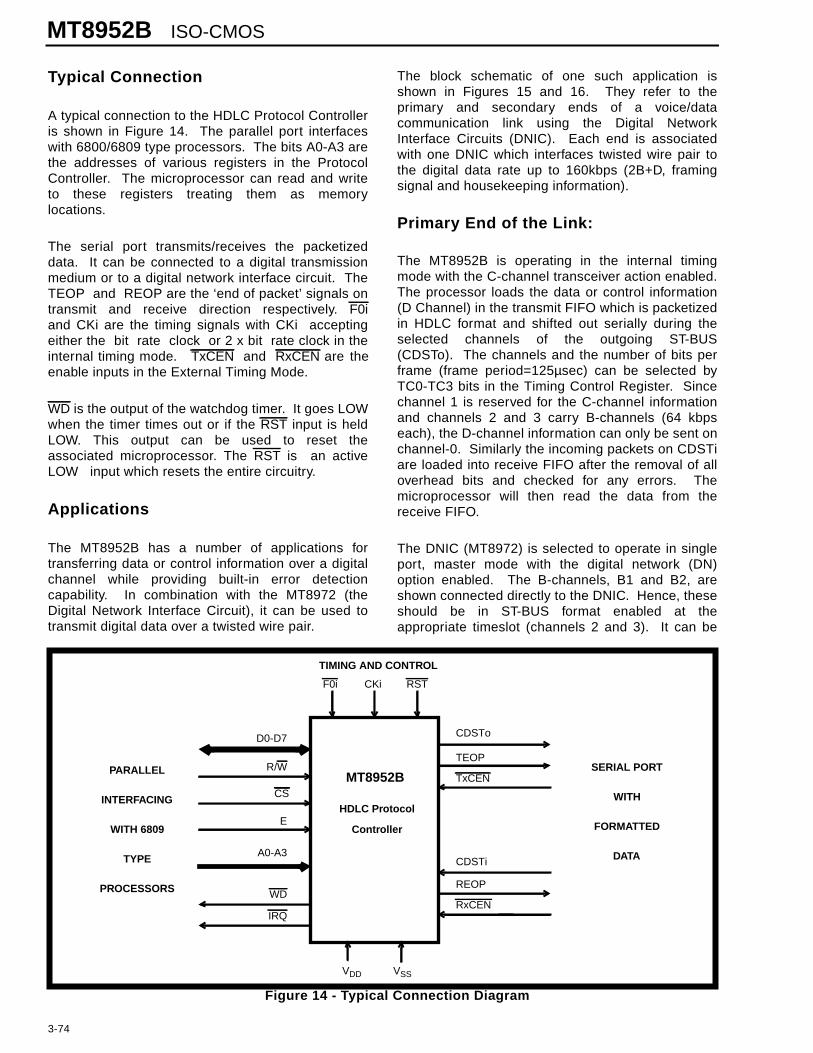
Typical Connection
A typical connection to the HDLC Protocol Controlleris shown in Figure 14. The parallel port interfaceswith 6800/6809 type processors. The bits A0-A3 arethe addresses of various registers in the ProtocolController. The microprocessor can read and writeto these registers treating them as memorylocations.
The serial port transmits/receives the packetizeddata. It can be connected to a digital transmissionmedium or to a digital network interface circuit. TheTEOP and REOP are the ‘end of packet’ signals ontransmit and receive direction respectively. F0iand CKi are the timing signals with CKi acceptingeither the bit rate clock or 2 x bit rate clock in theinternal timing mode. TxCEN and RxCEN are theenable inputs in the External Timing Mode.
WD is the output of the watchdog timer. It goes LOWwhen the timer times out or if the RST input is heldLOW. This output can be used to reset theassociated microprocessor. The RST is an activeLOW input which resets the entire circuitry.
Applications
The MT8952B has a number of applications fortransferring data or control information over a digitalchannel while providing built-in error detectioncapability. In combination with the MT8972 (theDigital Network Interface Circuit), it can be used totransmit digital data over a twisted wire pair.
The block schematic of one such application isshown in Figures 15 and 16. They refer to theprimary and secondary ends of a voice/datacommunication link using the Digital NetworkInterface Circuits (DNIC). Each end is associatedwith one DNIC which interfaces twisted wire pair tothe digital data rate up to 160kbps (2B+D, framingsignal and housekeeping information).
Primary End of the Link:
The MT8952B is operating in the internal timingmode with the C-channel transceiver action enabled.The processor loads the data or control information(D Channel) in the transmit FIFO which is packetizedin HDLC format and shifted out serially during theselected channels of the outgoing ST-BUS(CDSTo). The channels and the number of bits perframe (frame period=125µsec) can be selected byTC0-TC3 bits in the Timing Control Register. Sincechannel 1 is reserved for the C-channel informationand channels 2 and 3 carry B-channels (64 kbpseach), the D-channel information can only be sent onchannel-0. Similarly the incoming packets on CDSTiare loaded into receive FIFO after the removal of alloverhead bits and checked for any errors. Themicroprocessor will then read the data from thereceive FIFO.
The DNIC (MT8972) is selected to operate in singleport, master mode with the digital network (DN)option enabled. The B-channels, B1 and B2, areshown connected directly to the DNIC. Hence, theseshould be in ST-BUS format enabled at theappropriate timeslot (channels 2 and 3). It can be
Figure 14 - Typical Connection Diagram
PARALLEL
INTERFACING
WITH 6809
TYPE
PROCESSORS
SERIAL PORT
WITH
FORMATTED
DATA
D0-D7
R/W
CS
E
A0-A3
WD
IRQ
CDSTo
TEOP
TxCEN
CDSTi
REOP
RxCEN
MT8952B
HDLC Protocol
Controller
F0i CKi RST
VDD VSS
TIMING AND CONTROL

ISO-CMOS MT8952B
3-75
Figure 15 - HDLC Protocol Controller at the Primary End of the Link
Figure 16 - HDLC Protocol Controller at the Secondary End of the Link
MICROPROCESSOR
D0-D7
R/W
CS
E
A0-A3
WD
RST
IRQ
CDSTo
CDSTi
DSTi
DSTo
C4
F0
MS00
MS10
MS20
B-CHANNELS (2 X 64 kbits/sec Max)
MT8952B
HDLC PROTOCOL
CONTROLLER
MT8972
DIGITAL
NETWORK
INTERFACE
CIRCUIT
F0i CKi
TOTWISTED
WIRE PAIR
(160 kbits/sec)
Primary Terminal End Network Interface Network
MICROPROCESSOR
D0-D7
R/W
CS
E
A0-A3
WD
RST
IRQ
CDSTo
CDSTi
DSTi
DSTo
C4
F0
MS00
MS10
MS21
F0i CKi
B-CHANNELS (2 X 64 kbits/sec Max)
MT8952B
HDLC PROTOCOL
CONTROLLER
MT8972
DIGITAL
NETWORK
INTERFACE
CIRCUIT
TOTWISTED
WIRE PAIR
(160 kbits/sec)
Secondary Terminal End Network Interface Network
the outputs of voice codecs (MT896X) providingvoice communication or data codecs (MT8950) forcommunication between RS232-C type terminals. Itis possible to use the HDLC protocol on B1 and B2channels to provide the error detection.
This can be done by using a separate MT8952Benabled appropriately to shift out the formatted dataduring channels 2 and 3 or by multiplexing the sameMT8952B between B- and D- channels.
MT8952B ISO-CMOS
3-76
Secondary End of the Link:
At the secondary end of the communication link, asimilar procedure is adopted to transmit/receive thedata and control information.
The MT8952B operates in the Internal Timing Modeas at the primary end, but the DNIC (MT8972) isselected to operate in single port, slave mode withthe digital network capability enabled.
The other functions and procedures are similar tothose at the primary end.
The timing signals like CKi (C2i or C4i) and F0iare provided externally at the primary end and at thesecondary end, they are derived from the receiveddata.
Although this application describes thecommunication between two stations over adedicated link, it can be modified to serve a switchedcommunication path by additional control functionsand a call set-up procedure many of which can beachieved in software.
ISO-CMOS MT8952B
3-77
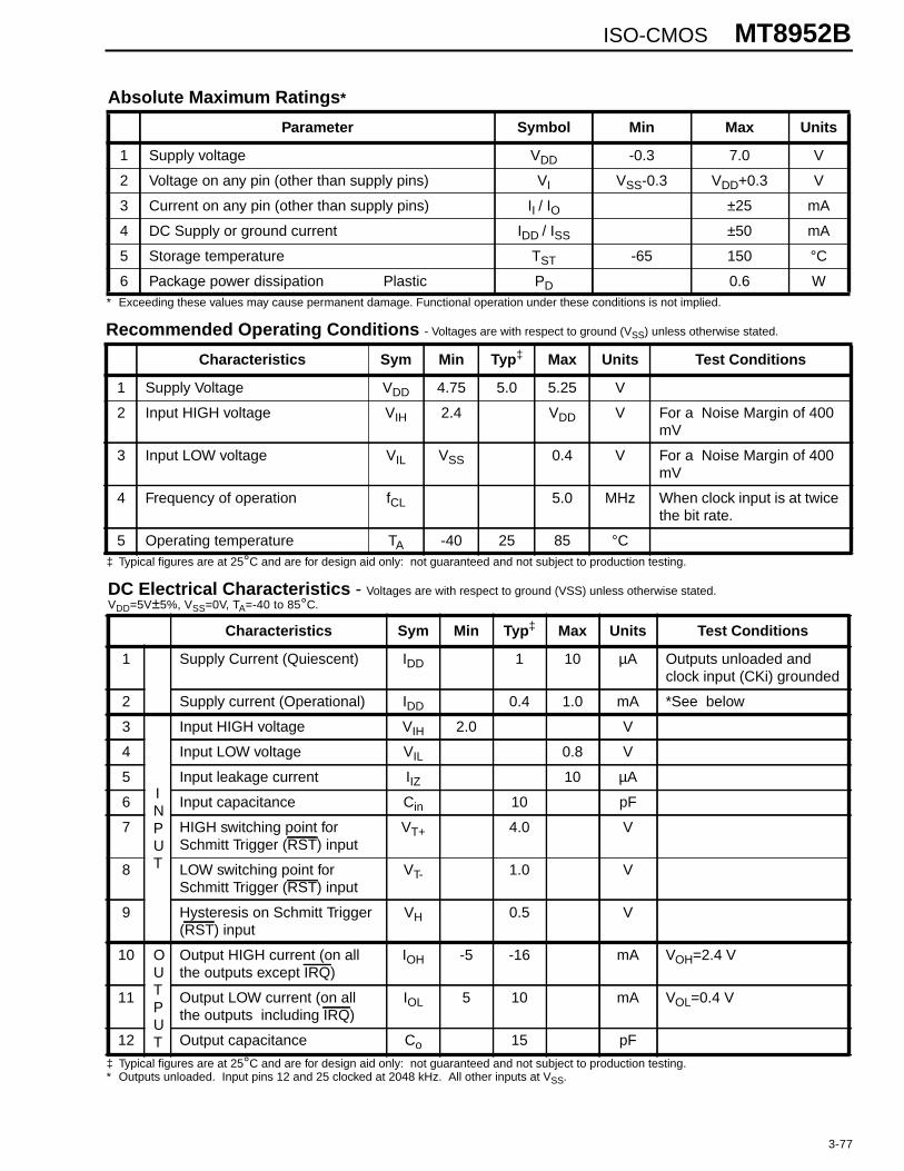
* Exceeding these values may cause permanent damage. Functional operation under these conditions is not implied.
‡ Typical figures are at 25°C and are for design aid only: not guaranteed and not subject to production testing.
‡ Typical figures are at 25°C and are for design aid only: not guaranteed and not subject to production testing.* Outputs unloaded. Input pins 12 and 25 clocked at 2048 kHz. All other inputs at VSS.
Absolute Maximum Ratings *
Parameter Symbol Min Max Units
1 Supply voltage VDD -0.3 7.0 V
2 Voltage on any pin (other than supply pins) VI VSS-0.3 VDD+0.3 V
3 Current on any pin (other than supply pins) II / IO ±25 mA
4 DC Supply or ground current IDD / ISS ±50 mA
5 Storage temperature TST -65 150 °C
6 Package power dissipation Plastic PD 0.6 W
Recommended Operating Conditions - Voltages are with respect to ground (VSS) unless otherwise stated.
Characteristics Sym Min Typ ‡ Max Units Test Conditions
1 Supply Voltage VDD 4.75 5.0 5.25 V
2 Input HIGH voltage VIH 2.4 VDD V For a Noise Margin of 400mV
3 Input LOW voltage VIL VSS 0.4 V For a Noise Margin of 400mV
4 Frequency of operation fCL 5.0 MHz When clock input is at twicethe bit rate.
5 Operating temperature TA -40 25 85 °C
DC Electrical Characteristics - Voltages are with respect to ground (VSS) unless otherwise stated.VDD=5V±5%, VSS=0V, TA=-40 to 85°C.
Characteristics Sym Min Typ ‡ Max Units Test Conditions
1 Supply Current (Quiescent) IDD 1 10 µA Outputs unloaded andclock input (CKi) grounded
2 Supply current (Operational) IDD 0.4 1.0 mA *See below
3
INPUT
Input HIGH voltage VIH 2.0 V
4 Input LOW voltage VIL 0.8 V
5 Input leakage current IIZ 10 µA
6 Input capacitance Cin 10 pF
7 HIGH switching point forSchmitt Trigger (RST) input
VT+ 4.0 V
8 LOW switching point forSchmitt Trigger (RST) input
VT- 1.0 V
9 Hysteresis on Schmitt Trigger(RST) input
VH 0.5 V
10 OUTPUT
Output HIGH current (on allthe outputs except IRQ)
IOH -5 -16 mA VOH=2.4 V
11 Output LOW current (on allthe outputs including IRQ)
IOL 5 10 mA VOL=0.4 V
12 Output capacitance Co 15 pF

MT8952B ISO-CMOS
3-78
† Timing is over recommended temperature & power supply voltages (VDD=5V±5%, VSS=0V, TA=–40 to 85°C).‡ Typical figures are at 25°C and are for design aid only: not guaranteed and not subject to production testing.
Figure 17 - Timing Information for MPU Write
AC Electrical Characteristics † - Microprocessor Interface - (Figures 17 and 18)Voltages are with respect to ground (VSS) unless otherwise stated.
Characteristics Sym Min Typ ‡ Max Units Test Conditions
1 Delay between CS and E clock tCSE 0 ns
2 Cycle time tCYC 205 ns
3 E Clock pulse width HIGH tEWH 145 ns
4 E Clock pulse width LOW tEWL 60 ns
5 Read/Write setup time tRWS 20 ns
6 Read/Write hold time tRWH 10 ns
7 Address setup time tAS 20 ns
8 Address hold time tAH 60 ns
9 Data setup time (write) tDSW 35 ns
10 Data hold time (write) tDHW 10 ns
11 E clock to valid data delay tDZLtDZH
145ns
Test load circuit 1 (Fig. 26)CL=200pF
12 Data hold time (read) tDLZtDHZ
10 60ns Test load circuit 3 (Fig. 26)
CS
E
CS
E
R/W
A0-A3
D0-D7
NOTE: The write cycle can be initiated either by the falling edge of CS or the rising edge of E clock whichever occurs last. Similarlythe cycle can be terminated by CS (rising edge) or E clock (falling edge) whichever occurs first. The timing relations are to bereferenced from the active edge initiating or terminating the cycle
tCSE tEWH
tEWL
tr tftCYC
tCSE
tRWS tRWH
tAS tAH
tDSW tDHW
E clock initiates andterminates the write cycle
CS initiates andterminates the write cycle

ISO-CMOS MT8952B
3-79
Figure 18 - Timing Information for MPU Read
Figure 19 - Interrupt Request Release Time
Figure 20 - Watchdog Timer Input and Output
CS
E
CS
E
R/W
A0-A3
D0-D7
E clock initiates andterminates the read cycle
CS initiates andterminates the read cycle
VALID DATAHigh Impedance High Impedance
tCSE tEWH
tr tftCYC
tCSE
tRWS tRWH
tAS tAH
tDZLtDZH
tDLZtDHZ
tEWL
NOTE: The read cycle cn be initiated either by the falling edge of CS or the rising edge of E clock whichever occurs last. Similarlythe cycle can be terminated by CS (rising edge) or E clock (falling edge) whichever occurs first. The timing relations are to bereferenced from the active edge initiating or terminating the cycle.
E
IRQ
tIRQR
F0i
WD
tWDHL tWDLH
MT8952B ISO-CMOS
3-80
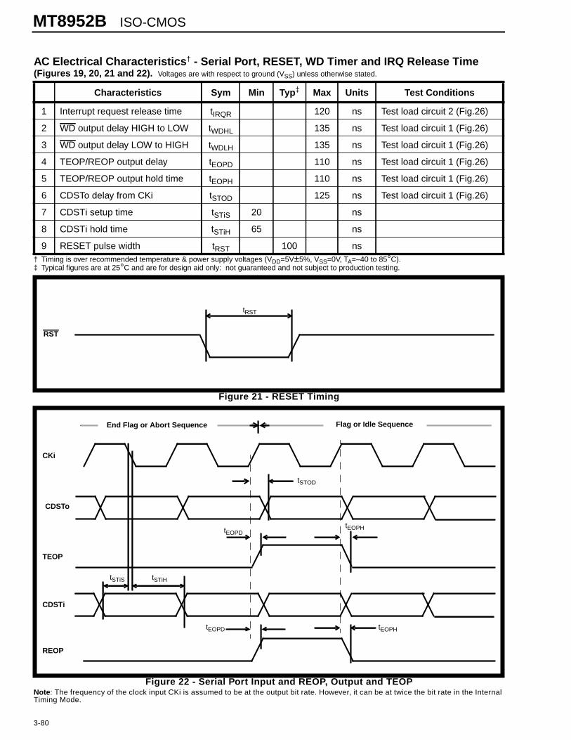
† Timing is over recommended temperature & power supply voltages (VDD=5V±5%, VSS=0V, TA=–40 to 85°C).‡ Typical figures are at 25°C and are for design aid only: not guaranteed and not subject to production testing.
Figure 21 - RESET Timing
Figure 22 - Serial Port Input and REOP, Output and TEOPNote : The frequency of the clock input CKi is assumed to be at the output bit rate. However, it can be at twice the bit rate in the InternalTiming Mode.
AC Electrical Characteristics † - Serial Port, RESET, WD Timer and IRQ Release Time(Figures 19, 20, 21 and 22). Voltages are with respect to ground (VSS) unless otherwise stated.
Characteristics Sym Min Typ ‡ Max Units Test Conditions
1 Interrupt request release time tIRQR 120 ns Test load circuit 2 (Fig.26)
2 WD output delay HIGH to LOW tWDHL 135 ns Test load circuit 1 (Fig.26)
3 WD output delay LOW to HIGH tWDLH 135 ns Test load circuit 1 (Fig.26)
4 TEOP/REOP output delay tEOPD 110 ns Test load circuit 1 (Fig.26)
5 TEOP/REOP output hold time tEOPH 110 ns Test load circuit 1 (Fig.26)
6 CDSTo delay from CKi tSTOD 125 ns Test load circuit 1 (Fig.26)
7 CDSTi setup time tSTiS 20 ns
8 CDSTi hold time tSTiH 65 ns
9 RESET pulse width tRST 100 ns
RST
tRST
CKi
CDSTo
TEOP
CDSTi
REOP
End Flag or Abort Sequence Flag or Idle Sequence
tSTOD
tEOPDtEOPH
tSTiS tSTiH
tEOPD tEOPH
ISO-CMOS MT8952B
3-81
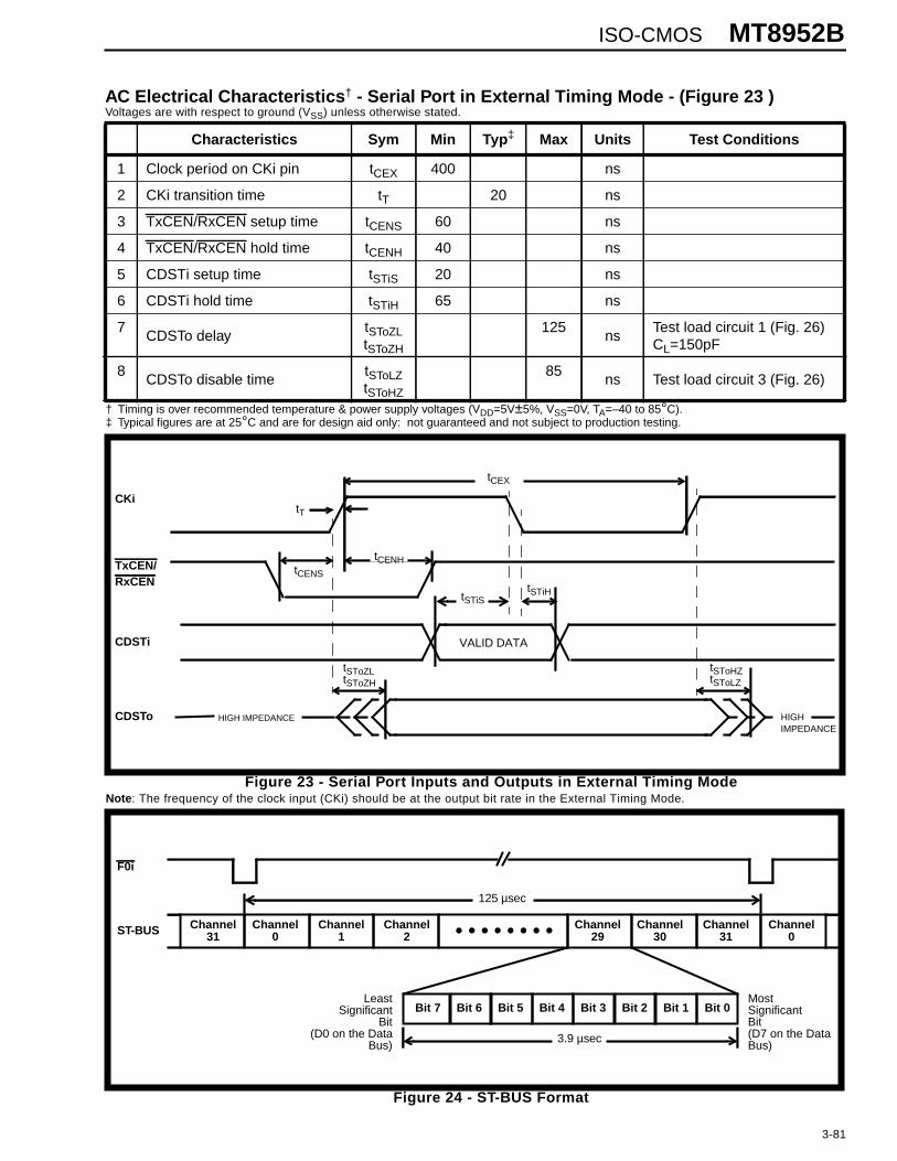
† Timing is over recommended temperature & power supply voltages (VDD=5V±5%, VSS=0V, TA=–40 to 85°C).‡ Typical figures are at 25°C and are for design aid only: not guaranteed and not subject to production testing.
Figure 23 - Serial Port Inputs and Outputs in External Timing ModeNote : The frequency of the clock input (CKi) should be at the output bit rate in the External Timing Mode.
Figure 24 - ST-BUS Format
AC Electrical Characteristics † - Serial Port in External Timing Mode - (Figure 23 )Voltages are with respect to ground (VSS) unless otherwise stated.
Characteristics Sym Min Typ ‡ Max Units Test Conditions
1 Clock period on CKi pin tCEX 400 ns
2 CKi transition time tT 20 ns
3 TxCEN/RxCEN setup time tCENS 60 ns
4 TxCEN/RxCEN hold time tCENH 40 ns
5 CDSTi setup time tSTiS 20 ns
6 CDSTi hold time tSTiH 65 ns
7CDSTo delay
tSToZLtSToZH
125ns
Test load circuit 1 (Fig. 26)CL=150pF
8CDSTo disable time
tSToLZtSToHZ
85ns Test load circuit 3 (Fig. 26)
CKi
TxCEN/RxCEN
CDSTi
CDSTo
VALID DATA
tCEX
tT
tCENS
tCENH
tSTiStSTiH
tSToZLtSToZH
tSToHZtSToLZ
HIGHIMPEDANCE
HIGH IMPEDANCE
Channel0
Channel1
Channel2 • • • • • • • •
Bit 7 Bit 6 Bit 5 Bit 4 Bit 3 Bit 2 Bit 1 Bit 0
125 µsec
Channel31
Channel30
Channel31
Channel0
Channel29
F0i
ST-BUS
LeastSignificant
Bit
MostSignificantBit
3.9 µsec(D0 on the DataBus)
(D7 on the DataBus)
MT8952B ISO-CMOS
3-82
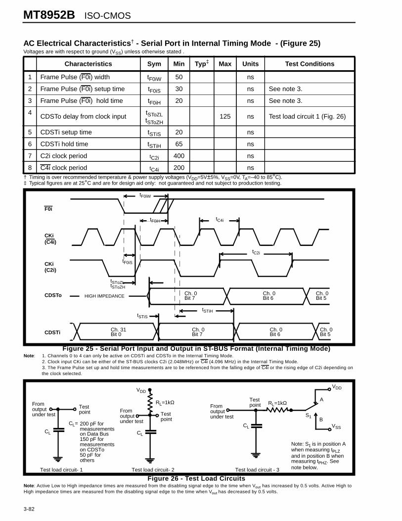
† Timing is over recommended temperature & power supply voltages (VDD=5V±5%, VSS=0V, TA=–40 to 85°C).‡ Typical figures are at 25°C and are for design aid only: not guaranteed and not subject to production testing.
Figure 25 - Serial Port Input and Output in ST-BUS Format (Internal Timing Mode)Note : 1. Channels 0 to 4 can only be active on CDSTi and CDSTo in the Internal Timing Mode.
2. Clock input CKi can be either of the ST-BUS clocks C2i (2.048MHz) or C4i (4.096 MHz) in the Internal Timing Mode.3. The Frame Pulse set up and hold time measurements are to be referenced from the falling edge of C4i or the rising edge of C2i depending onthe clock selected.
Figure 26 - Test Load CircuitsNote : Active Low to High impedance times are measured from the disabling signal edge to the time when Vout has increased by 0.5 volts. Active High toHigh impedance times are measured from the disabling signal edge to the time when Vout has decreased by 0.5 volts.
AC Electrical Characteristics † - Serial Port in Internal Timing Mode - (Figure 25)Voltages are with respect to ground (VSS) unless otherwise stated .
Characteristics Sym Min Typ ‡ Max Units Test Conditions
1 Frame Pulse (F0i) width tF0iW 50 ns
2 Frame Pulse (F0i) setup time tF0iS 30 ns See note 3.
3 Frame Pulse (F0i) hold time tF0iH 20 ns See note 3.
4CDSTo delay from clock input
tSToZLtSToZH
125 ns Test load circuit 1 (Fig. 26)
5 CDSTi setup time tSTiS 20 ns
6 CDSTi hold time tSTiH 65 ns
7 C2i clock period tC2i 400 ns
8 C4i clock period tC4i 200 ns
F0i
CKi(C4i)
CKi(C2i)
CDSTo
CDSTi
tF0iW
tF0iH tC4i
tF0iS
tC2i
tSToZLtSToZH
HIGH IMPEDANCE Ch. 0Bit 7
Ch. 0Bit 6
Ch. 0Bit 5
tSTiHtSTiS
Ch. 31Bit 0
Ch. 0Bit 7
Ch. 0Bit 6
Ch. 0Bit 5
Fromoutputunder test
Testpoint
CL
Test load circuit- 1
VDD
RL=1kΩ
Testpoint
Fromoutputunder test
Test load circuit- 2 Test load circuit - 3
Fromoutputunder test
CLCL
Testpoint
S1
VDD
VSS
RL=1kΩ
Note: S1 is in position Awhen measuring tPLZand in position B whenmeasuring tPHZ. Seenote below.
CL= 200 pF for
on Data Bus150 pF formeasurementson CDSTo50 pF forothers
measurements
A
B
Package Outlines
Lead SOIC Package - S Suffix
NOTES: 1. Controlling dimensions in parenthesis ( ) are in millimeters.2. Converted inch dimensions are not necessarily exact.
DIM16-Pin 18-Pin 20-Pin 24-Pin 28-Pin
Min Max Min Max Min Max Min Max Min Max
A 0.093(2.35)
0.104(2.65)
0.093(2.35)
0.104(2.65)
0.093(2.35)
0.104(2.65)
0.093(2.35)
0.104(2.65)
0.093(2.35)
0.104(2.65)
A1 0.004(0.10)
0.012(0.30)
0.004(0.10)
0.012(0.30)
0.004(0.10)
0.012(0.30)
0.004(0.10)
0.012(0.30)
0.004(0.10)
0.012(0.30)
B 0.013(0.33)
0.020(0.51)
0.013(0.33)
0.030(0.51)
0.013(0.33)
0.020(0.51)
0.013(0.33)
0.020(0.51)
0.013(0.33)
0.020(0.51)
C 0.009(0.231)
0.013(0.318)
0.009(0.231)
0.013(0.318)
0.009(0.231)
0.013(0.318)
0.009(0.231)
0.013(0.318)
0.009(0.231)
0.013(0.318)
D 0.398(10.1)
0.413(10.5)
0.447(11.35)
0.4625(11.75)
0.496(12.60)
0.512(13.00)
0.5985(15.2)
0.614(15.6)
0.697(17.7)
0.7125(18.1)
E 0.291(7.40)
0.299(7.40)
0.291(7.40)
0.299(7.40)
0.291(7.40)
0.299(7.40)
0.291(7.40)
0.299(7.40)
0.291(7.40)
0.299(7.40)
e 0.050 BSC(1.27 BSC)
0.050 BSC(1.27 BSC)
0.050 BSC(1.27 BSC)
0.050 BSC(1.27 BSC)
0.050 BSC(1.27 BSC)
H 0.394(10.00)
0.419(10.65)
0.394(10.00)
0.419(10.65)
0.394(10.00)
0.419(10.65)
0.394(10.00)
0.419(10.65)
0.394(10.00)
0.419(10.65)
L 0.016(0.40)
0.050(1.27)
0.016(0.40)
0.050(1.27)
0.016(0.40)
0.050(1.27)
0.016(0.40)
0.050(1.27)
0.016(0.40)
0.050(1.27)
Pin 1
A1
B
e
E
A
L
H
C
Notes:1) Not to scale2) Dimensions in inches3) (Dimensions in millimeters)4) A & B Maximum dimensions include allowable mold flash
D L
4 mils (lead coplanarity)
General-7
Package Outlines
Plastic J-Lead Chip Carrier - P-Suffix
F
D1D
H
E1
I
A1
A
G
D2
E
E2
Dim20-Pin 28-Pin 44-Pin 68-Pin 84-Pin
Min Max Min Max Min Max Min Max Min Max
A 0.165(4.20)
0.180(4.57)
0.165(4.20)
0.180(4.57)
0.165(4.20)
0.180(4.57)
0.165(4.20)
0.200(5.08)
0.165(4.20)
0.200(5.08)
A1 0.090(2.29)
0.120(3.04)
0.090(2.29)
0.120(3.04)
0.090(2.29)
0.120(3.04)
0.090(2.29)
0.130(3.30)
0.090(2.29)
0.130(3.30)
D/E 0.385(9.78)
0.395(10.03)
0.485(12.32)
0.495(12.57)
0.685(17.40)
0.695(17.65)
0.985(25.02)
0.995(25.27)
1.185(30.10)
1.195(30.35)
D1/E1 0.350(8.890)
0.356(9.042)
0.450(11.430)
0.456(11.582)
0.650(16.510)
0.656(16.662)
0.950(24.130)
0.958(24.333)
1.150(29.210)
1.158(29.413)
D2/E2 0.290(7.37)
0.330(8.38)
0.390(9.91)
0.430(10.92)
0.590(14.99)
0.630(16.00)
0.890(22.61)
0.930(23.62)
1.090(27.69)
1.130(28.70)
e 0 0.004 0 0.004 0 0.004 0 0.004 0 0.004
F 0.026(0.661)
0.032(0.812)
0.026(0.661)
0.032(0.812)
0.026(0.661)
0.032(0.812)
0.026(0.661)
0.032(0.812)
0.026(0.661)
0.032(0.812)
G 0.013(0.331)
0.021(0.533)
0.013(0.331)
0.021(0.533)
0.013(0.331)
0.021(0.533)
0.013(0.331)
0.021(0.533)
0.013(0.331)
0.021(0.533)
H 0.050 BSC(1.27 BSC)
0.050 BSC(1.27 BSC)
0.050 BSC(1.27 BSC)
0.050 BSC(1.27 BSC)
0.050 BSC(1.27 BSC)
I 0.020(0.51)
0.020(0.51)
0.020(0.51)
0.020(0.51)
0.020(0.51)
Notes:1) Not to scale2) Dimensions in inches3) (Dimensions in millimeters)4) For D & E add for allowable Mold Protrusion 0.010"
e: (lead coplanarity)
General-10
Package Outlines
Plastic Dual-In-Line Packages (PDIP) - E Suffix
NOTE: Controlling dimensions in parenthesis ( ) are in millimeters.
DIM
8-Pin 16-Pin 18-Pin 20-Pin
Plastic Plastic Plastic Plastic
Min Max Min Max Min Max Min Max
A 0.210 (5.33) 0.210 (5.33) 0.210 (5.33) 0.210 (5.33)
A2 0.115 (2.92) 0.195 (4.95) 0.115 (2.92) 0.195 (4.95) 0.115 (2.92) 0.195 (4.95) 0.115 (2.92) 0.195 (4.95)
b 0.014 (0.356) 0.022 (0.558) 0.014 (0.356) 0.022 (0.558) 0.014 (0.356) 0.022 (0.558) 0.014 (0.356) 0.022 (0.558)
b2 0.045 (1.14) 0.070 (1.77) 0.045 (1.14) 0.070 (1.77) 0.045 (1.14) 0.070 (1.77) 0.045 (1.14) 0.070 (1.77)
C 0.008(0.203)
0.014 (0.356) 0.008 (0.203) 0.014(0.356) 0.008 (0.203) 0.014 (0.356) 0.008 (0.203) 0.014 (0.356)
D 0.355 (9.02) 0.400 (10.16) 0.780 (19.81) 0.800 (20.32) 0.880 (22.35) 0.920 (23.37) 0.980 (24.89) 1.060 (26.9)
D1 0.005 (0.13) 0.005 (0.13) 0.005 (0.13) 0.005 (0.13)
E 0.300 (7.62) 0.325 (8.26) 0.300 (7.62) 0.325 (8.26) 0.300 (7.62) 0.325 (8.26) 0.300 (7.62) 0.325 (8.26)
E1 0.240 (6.10) 0.280 (7.11) 0.240 (6.10) 0.280 (7.11) 0.240 (6.10) 0.280 (7.11) 0.240 (6.10) 0.280 (7.11)
e 0.100 BSC (2.54) 0.100 BSC (2.54) 0.100 BSC (2.54) 0.100 BSC (2.54)
eA 0.300 BSC (7.62) 0.300 BSC (7.62) 0.300 BSC (7.62) 0.300 BSC (7.62)
L 0.115 (2.92) 0.150 (3.81) 0.115 (2.92) 0.150 (3.81) 0.115 (2.92) 0.150 (3.81) 0.115 (2.92) 0.150 (3.81)
eB 0.430 (10.92) 0.430 (10.92) 0.430 (10.92) 0.430 (10.92)
eC 0 0.060 (1.52) 0 0.060 (1.52) 0 0.060 (1.52) 0 0.060 (1.52)
E1
3 2 1
E
n-2 n-1 n
L
D
D1
b2
A2
e
b
C
eA
Notes:1) Not to scale2) Dimensions in inches3) (Dimensions in millimeters)
A
eB
eC
General-8
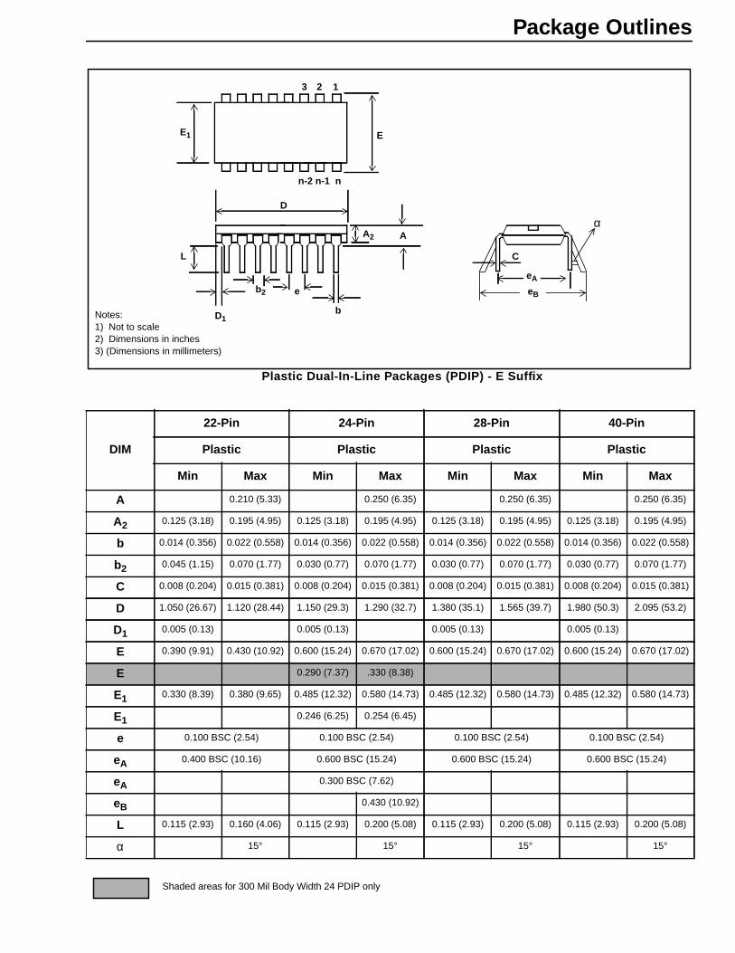
Package Outlines
Plastic Dual-In-Line Packages (PDIP) - E Suffix
DIM
22-Pin 24-Pin 28-Pin 40-Pin
Plastic Plastic Plastic Plastic
Min Max Min Max Min Max Min Max
A 0.210 (5.33) 0.250 (6.35) 0.250 (6.35) 0.250 (6.35)
A2 0.125 (3.18) 0.195 (4.95) 0.125 (3.18) 0.195 (4.95) 0.125 (3.18) 0.195 (4.95) 0.125 (3.18) 0.195 (4.95)
b 0.014 (0.356) 0.022 (0.558) 0.014 (0.356) 0.022 (0.558) 0.014 (0.356) 0.022 (0.558) 0.014 (0.356) 0.022 (0.558)
b2 0.045 (1.15) 0.070 (1.77) 0.030 (0.77) 0.070 (1.77) 0.030 (0.77) 0.070 (1.77) 0.030 (0.77) 0.070 (1.77)
C 0.008 (0.204) 0.015 (0.381) 0.008 (0.204) 0.015 (0.381) 0.008 (0.204) 0.015 (0.381) 0.008 (0.204) 0.015 (0.381)
D 1.050 (26.67) 1.120 (28.44) 1.150 (29.3) 1.290 (32.7) 1.380 (35.1) 1.565 (39.7) 1.980 (50.3) 2.095 (53.2)
D1 0.005 (0.13) 0.005 (0.13) 0.005 (0.13) 0.005 (0.13)
E 0.390 (9.91) 0.430 (10.92) 0.600 (15.24) 0.670 (17.02) 0.600 (15.24) 0.670 (17.02) 0.600 (15.24) 0.670 (17.02)
E 0.290 (7.37) .330 (8.38)
E1 0.330 (8.39) 0.380 (9.65) 0.485 (12.32) 0.580 (14.73) 0.485 (12.32) 0.580 (14.73) 0.485 (12.32) 0.580 (14.73)
E1 0.246 (6.25) 0.254 (6.45)
e 0.100 BSC (2.54) 0.100 BSC (2.54) 0.100 BSC (2.54) 0.100 BSC (2.54)
eA 0.400 BSC (10.16) 0.600 BSC (15.24) 0.600 BSC (15.24) 0.600 BSC (15.24)
eA 0.300 BSC (7.62)
eB 0.430 (10.92)
L 0.115 (2.93) 0.160 (4.06) 0.115 (2.93) 0.200 (5.08) 0.115 (2.93) 0.200 (5.08) 0.115 (2.93) 0.200 (5.08)
α 15° 15° 15° 15°
E1
3 2 1
E
n-2 n-1 n
L
D
D1
b2
A2
e
b
C
eA
Notes:1) Not to scale2) Dimensions in inches3) (Dimensions in millimeters)
A
eB
α
Shaded areas for 300 Mil Body Width 24 PDIP only

M Mitel (design) and ST-BUS are registered trademarks of MITEL CorporationMitel Semiconductor is an ISO 9001 Registered CompanyCopyright 1999 MITEL CorporationAll Rights ReservedPrinted in CANADA
TECHNICAL DOCUMENTATION - NOT FOR RESALE
World Headquarters - CanadaTel: +1 (613) 592 2122Fax: +1 (613) 592 6909
North America Asia/Pacific Europe, Middle East,Tel: +1 (770) 486 0194 Tel: +65 333 6193 and Africa (EMEA)Fax: +1 (770) 631 8213 Fax: +65 333 6192 Tel: +44 (0) 1793 518528
Fax: +44 (0) 1793 518581
http://www.mitelsemi.com
Information relating to products and services furnished herein by Mitel Corporation or its subsidiaries (collectively “Mitel”) is believed to be reliable. However, Mitel assumes noliability for errors that may appear in this publication, or for liability otherwise arising from the application or use of any such information, product or service or for any infringement ofpatents or other intellectual property rights owned by third parties which may result from such application or use. Neither the supply of such information or purchase of product orservice conveys any license, either express or implied, under patents or other intellectual property rights owned by Mitel or licensed from third parties by Mitel, whatsoever.Purchasers of products are also hereby notified that the use of product in certain ways or in combination with Mitel, or non-Mitel furnished goods or services may infringe patents orother intellectual property rights owned by Mitel.
This publication is issued to provide information only and (unless agreed by Mitel in writing) may not be used, applied or reproduced for any purpose nor form part of any order orcontract nor to be regarded as a representation relating to the products or services concerned. The products, their specifications, services and other information appearing in thispublication are subject to change by Mitel without notice. No warranty or guarantee express or implied is made regarding the capability, performance or suitability of any product orservice. Information concerning possible methods of use is provided as a guide only and does not constitute any guarantee that such methods of use will be satisfactory in a specificpiece of equipment. It is the user’s responsibility to fully determine the performance and suitability of any equipment using such information and to ensure that any publication ordata used is up to date and has not been superseded. Manufacturing does not necessarily include testing of all functions or parameters. These products are not suitable for use inany medical products whose failure to perform may result in significant injury or death to the user. All products and materials are sold and services provided subject to Mitel’sconditions of sale which are available on request.