Embed Size (px)
Citation preview

IS31FL3726
Integrated Silicon Solution, Inc. — www.issi.com Rev.B, 06/18/2013
1
16-BIT COLOR LED DRIVER WITH PWM CONTROL June 2013
GENERAL DESCRIPTION The IS31FL3726 is comprised of constant-current drivers designed for color LEDs. The output current value can be set using an external resistor. The output current value can be adjusted from 5mA to 60mA through the external resistor.
As a result, all outputs will have virtually the same current levels.
This driver incorporates 16-bit constant t-current outputs, a 16-bit shift register, a 16-bit latch and a 16-bit AND-gate circuit.
These drivers have been designed using the CMOS process.
FEATURES Output current capability and number of outputs:
60mA × 16 outputs Constant current range: 5mA to 60mA Application output voltage: ≥0.4V For anode-common LEDs Power supply voltage range, VDD = 3.3V to 5.5V Serial and parallel data transfer rate: 20MHz
(Max. cascade connection) Operating temperature range, TA = −40°C ~
+85°C Package: QFN-24 and TSSOP-24 Current accuracy (All output on)
APPLICATIONAS
Cellular phones MP3/MP4/CD/minidiskplayers Toys BLOCK DIAGRAM
Figure 1 Block Diagram
Output voltage
Current Accuracy Output Current Between Bits Between ICs
≥0.4V ±4% ±20% 5mA ~ 60mA

IS31FL3726
Integrated Silicon Solution, Inc. — www.issi.com Rev.B, 06/18/2013
2
TYPICAL APPLICATION CIRCUIT
. .
. .
. .
MICROCONTROLLER
Vbat
O1
O2
O3
O16
O15
O14
RE
XT
GN
D
SERIAL-IN
ENABLE
LATCH
CLOCK
VD
D
R1=2kohm(tpy.)
0.1uF
LDO 3.3V
Figure 2 Typical Application Figure

IS31FL3726
Integrated Silicon Solution, Inc. — www.issi.com Rev.B, 06/18/2013
3
PIN CONFIGURATION
Package Pin Configuration (Top View)
QFN-24
1
2
3
4
24
14
15
16
17
23 22 21
7 8 9 10
5
11
18
20
6
12
13
19
LA
TC
H
OU
T0
OU
T1
OU
T2
OU
T3
OU
T4
OUT5
OUT6
OUT7
OUT8
OUT9
OUT10
VDD
CLOCK
GND
SERIAL-IN
R-EXT
SERIAL-OUT
OU
T11
OU
T12
OU
T13
OU
T14
OU
T15
EN
AB
LE
TSSOP-24

IS31FL3726
Integrated Silicon Solution, Inc. — www.issi.com Rev.B, 06/18/2013
4
PIN DESCRIPTION
No. Pin Description
QFN TSSOP
1 22 SERIAL-OUT Output terminal for serial data input on SERIAL-IN terminal.
2 23 R-EXT Input terminal used to connect an external resistor. This regulated the output current.
3 24 VDD Supply voltage terminal.
4 1 GND GND terminal for control logic.
5 2 SERIAL-IN Input terminal for serial data for data shift register.
6 3 CLOCK Input terminal for clock for data shift on rising edge.
7 4 LA T CH————————
Input terminal for data strobe When the LA T CH
————————
input is driven High, data is not latched. When it is pulled Low ,data is latched.
8 ~ 23 5~20 OUT0——————
~OUT15———————
Constant-current output terminals.
24 21 ENABLE—————————
Input terminal for output enable.
All outputs (OUT0——————
to OUT15———————
) are turned off, when
the ENABLE—————————
terminal is driven High .And are turned on, when the terminal is driven Low.
Thermal Pad Connect to GND.

IS31FL3726
Integrated Silicon Solution, Inc. — www.issi.com Rev.B, 06/18/2013
5
ORDERING INFORMATION
Industrial Range: -40°C to +85°C
Order Part No. Package QTY/Reel
IS31FL3726-QFLS2-TR QFN-24, Lead-free 2500/Reel IS31FL3726-ZLS2-TR IS31FL3726-ZLS2
TSSOP-24, Lead-free 2500/Reel 62/Tube
Copyright © 2013 Integrated Silicon Solution, Inc. All rights reserved. ISSI reserves the right to make changes to this specification and its products at any time without notice. ISSI assumes no liability arising out of the application or use of any information, products or services described herein. Customers are advised to obtain the latest version of this device specification before relying on any published information and before placing orders for products. Integrated Silicon Solution, Inc. does not recommend the use of any of its products in life support applications where the failure or malfunction of the product can reasonably be expected to cause failure of the life support system or to significantly affect its safety or effectiveness. Products are not authorized for use in such applications unless Integrated Silicon Solution, Inc. receives written assurance to its satisfaction, that: a.) the risk of injury or damage has been minimized; b.) the user assume all such risks; and c.) potential liability of Integrated Silicon Solution, Inc is adequately protected under the circumstances

IS31FL3726
Integrated Silicon Solution, Inc. — www.issi.com Rev.B, 06/18/2013
6
n = 0 1 2 3 4 5 6 7 8 9 10 11 12 13 14 15
CLOCK
SERIAL-IN
LATCH
ENABLE
OUT0
OUT1
OUT2
OUT15
SERIAL-OUT
HL
HL
HL
HL
ONOFF
ONOFF
ONOFF
ONOFF
HL
Figure 3 Timing Dagram
Warning: Latch circuit is leveled-latch circuit. Be careful because it is not triggered-latch circuit.
Note : The latches circuit holds data by pulling the L A T C H————————
terminal Low. And, when L A T C H————————
terminal is a High level, latch circuit
doesn’t hold data, and it passes from the input to the output. When E N A B L E—————————
terminal is a Low level, output terminal O U T 0——————
to O U T 1 5———————
respond to the data, and on and off does. And, when E N A B L E—————————
terminal is a High level, it offs with the output terminal regardless of the data. Truth Table
CLOCK LA TC H————————
ENABLE—————————
SERIAL-IN OUT0——————
…OUT7——————
… OUT15———————
SERIAL-OUT
H L Dn Dn …Dn-7 …Dn-15 Dn-15
L L Dn+1 No change Dn-14
H L Dn+2 Dn+2 …Dn-5 …Dn-13 Dn-13
X L Dn+3 Dn+2 …Dn-5 …Dn-13 Dn-13
X H Dn+3 OFF Dn-13
Note : OUT0—————
to OUT15— — — — —
=On when Dn = H; OUT0—————
to OUT15— — — — —
=Off when Dn = L. In order to ensure that the level of the power supply voltage is correct, an external resistor must be connected between R-EXT and GND.
Warning: The following conditions, ENABLE____________
=0, LATCH__________
=1, SERIAL-IN=1, cannot be configured at the same time when power on, or IS31FL3726 will be abnormal.
IS31FL3726
Integrated Silicon Solution, Inc. — www.issi.com Rev.B, 06/18/2013
7
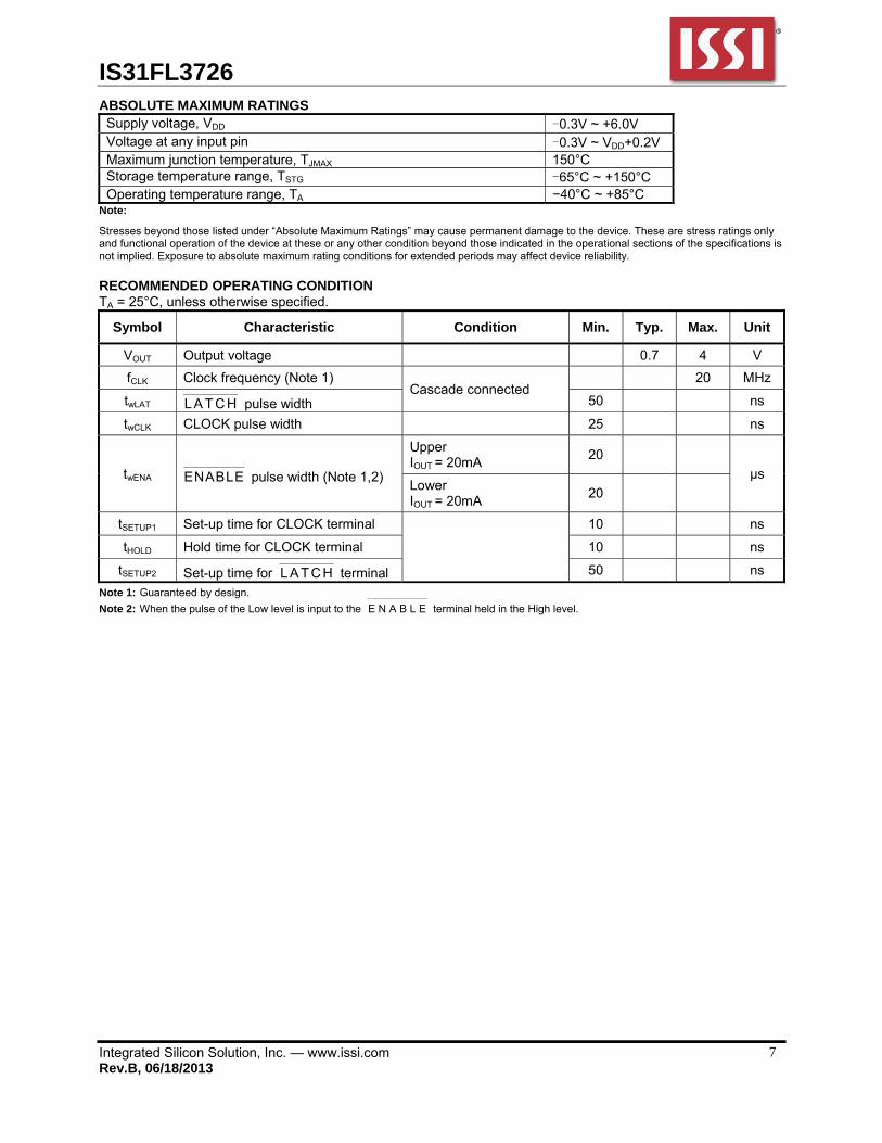
ABSOLUTE MAXIMUM RATINGS Supply voltage, VDD -0.3V ~ +6.0V Voltage at any input pin -0.3V ~ VDD+0.2V Maximum junction temperature, TJMAX 150°C Storage temperature range, TSTG -65°C ~ +150°C Operating temperature range, TA −40°C ~ +85°C
Note:
Stresses beyond those listed under “Absolute Maximum Ratings” may cause permanent damage to the device. These are stress ratings only and functional operation of the device at these or any other condition beyond those indicated in the operational sections of the specifications is not implied. Exposure to absolute maximum rating conditions for extended periods may affect device reliability. RECOMMENDED OPERATING CONDITION TA = 25°C, unless otherwise specified.
Symbol Characteristic Condition Min. Typ. Max. Unit
VOUT Output voltage 0.7 4 V
fCLK Clock frequency (Note 1) Cascade connected
20 MHz
twLAT LA T CH————————
pulse width 50 ns
twCLK CLOCK pulse width 25 ns
twENA ENABLE—————————
pulse width (Note 1,2)
Upper IOUT = 20mA
20
µs Lower IOUT = 20mA
20
tSETUP1 Set-up time for CLOCK terminal
10 ns
tHOLD Hold time for CLOCK terminal 10 ns
tSETUP2 Set-up time for LA T C H————————
terminal 50 ns
Note 1: Guaranteed by design.
Note 2: When the pulse of the Low level is input to the E N A B L E—————————
terminal held in the High level.
IS31FL3726
Integrated Silicon Solution, Inc. — www.issi.com Rev.B, 06/18/2013
8
ELECTRICAL CHARACTERISTICS TA = 25°C, VDD = 3.3V ~ 5.5V, unless otherwise specified.
Symbol Characteristic Condition Min. Typ. Max. Unit
VDD Supply voltage Normal operation 3.3 5.5 V
IOUT1
Output current
VOUT = 0.4V VDD = 3.3V
REXT = 1kΩ
15 18.7 22
mA
IOUT2 VOUT = 0.4V VDD = 5.5V
15 18.9 22
IOUT1 Output current error between bits
VOUT≥0.4V, All outputs on
REXT = 1kΩ ±3 ±4 %
IOZ Output leakage current input voltage
VOUT = 5.0V 1 uA
VIH Input voltage
1.4 V
VIL 0.4
VOL
SOUT terminal voltage
IOL = 1.0mA, VDD = 3.3V 0.3
V IOL = 1.0mA, VDD = 5V 0.3
VOH IOH = -1.0mA, VDD = 3.3V 3
IOH = -1.0mA, VDD = 5V 4.7
%/VDD Output current supply voltage regulation
When VDD is changed 3.3V to 5.5V
-1 %
R(Up) Pull-up resistor ENABLE—————————
terminal 250 500 750 kΩ
R(Down) Pull-down resistor LA T CH————————
terminal
IDD(OFF)1
Supply current
VOUT = 5V REXT = OPEN 1
mA IDD(OFF)2
VOUT = 5V All outputs off
REXT = 1kΩ 4.5
IDD(ON)1 VOUT = 0.7V All outputs on
REXT = 1kΩ 5

IS31FL3726
Integrated Silicon Solution, Inc. — www.issi.com Rev.B, 06/18/2013
9
SWITCHING CHARACTERISTICS TA = 25°C, unless otherwise specified.
Symbol Characteristic Condition Min. Typ. Max. Unit
tpLH1
Propagation delay
CLK-OUTn——————
, LA T C H————————
= “H”
ENABLE—————————
= “L” 80 200
ns
tpLH2 LA TC H————————
–OUTn——————
, ENABLE—————————
= “L” 80 200
tpLH3 ENABLE—————————
-OUTn——————
, LA T C H————————
= “H” 2000
tpLH CLK-SERIAL OUT 3 5
tpHL1 CLK-OUTn
——————
, LA T C H————————
= “H”
ENABLE—————————
= “L” 160 250
tpHL2 LA TC H————————
-OUTn——————
, ENABLE—————————
= “L” 160 250
tpHL3 ENABLE—————————
-OUTn——————
, LA T C H————————
= “H” 200 350
tpLH CLK-SERIAL OUT 4 6
tor Output rise time 10%~90% of voltage waveform 30 150 200 ns
tof Output fall time 90%~10% of voltage waveform 150 200 250 ns
tr Maximum CLOCK rise time When not on PCB (Note)
5 us
tf Maximum CLOCK fall time 5 us
Conditions: (Refer to test circuit.)
Topr = 25°C, VDD=VIH =3.3V and 5V, VOUT = 0.7V, VIL =0V, REXT =1000Ω, VL =3.0V, RL=60Ω, CL=10.5pF
Note:
1. If the device is connected in a cascade and tr/tf for the waveform is large, it may not be possible to achieve the timing required for data
transfer. Please consider the timings carefully.
2. Delay between outputs. The IS31FL3726 has graduated delay circuits between outputs. The fixed delay time is 5ns (typical), OUT1 has 5ns
delay, OUT2 has 10 ns delay, etc. This delay prevents large inrush currents, which reduce power supply bypass capacitor requirements when
the outputs turn on. The delay works during switch on and switch off of each output channel. LEDs that have not turned on before ENABLE———————
is
low will still turn on and off at the determined delayed time regardless of the state of ENABLE———————
. Therefore, every LED will be illuminated for the
amount of time ENABLE———————
is pulled high.
Figure 4 Test Diagram
IS31FL3726
Integrated Silicon Solution, Inc. — www.issi.com Rev.B, 06/18/2013
10
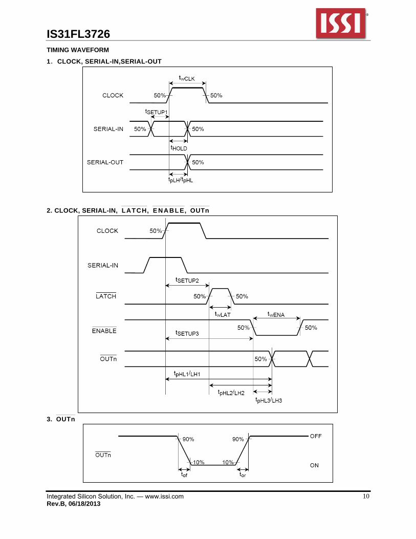
TIMING WAVEFORM
1.CLOCK, SERIAL-IN,SERIAL-OUT
2. CLOCK, SERIAL-IN, LATCH————————
, E N A BL E——————————
, OUTn——————
3. OUTn——————

IS31FL3726
Integrated Silicon Solution, Inc. — www.issi.com Rev.B, 06/18/2013
11
TYPICAL OPERATING CHARACTERISTICS
ADJUSTING OUTPUT CURRENT The output current of each channel is set by an external resistor Rext, the relationship between Iout and Rext is:
Iout = (VR-ext/Rext)×52 the VR-ext is 0.36V in the IS31FL3726,so we can count the Iout as :
Iout = 0.36×52/Rext. As show in the figure below:
10
15
20
25
30
35
40
45
50
400 600 800 1000 1200 1400 1600
Rset(Ω)
LED current(mA)
-40°C
25°C
85°C

IS31FL3726
Integrated Silicon Solution, Inc. — www.issi.com Rev.B, 06/18/2013
12
CLASSIFICATION REFLOW PROFILES
Profile Feature Pb-Free Assembly
Preheat & Soak Temperature min (Tsmin) Temperature max (Tsmax) Time (Tsmin to Tsmax) (ts)
150°C 200°C 60-120 seconds
Average ramp-up rate (Tsmax to Tp) 3°C/second max.
Liquidous temperature (TL) Time at liquidous (tL)
217°C 60-150 seconds
Peak package body temperature (Tp)* Max 260°C
Time (tp)** within 5°C of the specified classification temperature (Tc)
Max 30 seconds
Average ramp-down rate (Tp to Tsmax) 6°C/second max.
Time 25°C to peak temperature 8 minutes max.
Figure 5 Classification Profile

IS31FL3726
Integrated Silicon Solution, Inc. — www.issi.com Rev.B, 06/18/2013
13
PACKAGE INFORMATION
QFN-24
Note: All dimensions in millimeters unless otherwise stated.

IS31FL3726
Integrated Silicon Solution, Inc. — www.issi.com Rev.B, 06/18/2013
14
TSSOP-24
Note: All dimensions in millimeters unless otherwise stated.