Embed Size (px)
Citation preview

To learn more about ON Semiconductor, please visit our website at www.onsemi.com
Is Now Part of
ON Semiconductor and the ON Semiconductor logo are trademarks of Semiconductor Components Industries, LLC dba ON Semiconductor or its subsidiaries in the United States and/or other countries. ON Semiconductor owns the rights to a number of patents, trademarks, copyrights, trade secrets, and other intellectual property. A listing of ON Semiconductor’s product/patent coverage may be accessed at www.onsemi.com/site/pdf/Patent-Marking.pdf. ON Semiconductor reserves the right to make changes without further notice to any products herein. ON Semiconductor makes no warranty, representation or guarantee regarding the suitability of its products for any particular purpose, nor does ON Semiconductor assume any liability arising out of the application or use of any product or circuit, and specifically disclaims any and all liability, including without limitation special, consequential or incidental damages. Buyer is responsible for its products and applications using ON Semiconductor products, including compliance with all laws, regulations and safety requirements or standards, regardless of any support or applications information provided by ON Semiconductor. “Typical” parameters which may be provided in ON Semiconductor data sheets and/or specifications can and do vary in different applications and actual performance may vary over time. All operating parameters, including “Typicals” must be validated for each customer application by customer’s technical experts. ON Semiconductor does not convey any license under its patent rights nor the rights of others. ON Semiconductor products are not designed, intended, or authorized for use as a critical component in life support systems or any FDA Class 3 medical devices or medical devices with a same or similar classification in a foreign jurisdiction or any devices intended for implantation in the human body. Should Buyer purchase or use ON Semiconductor products for any such unintended or unauthorized application, Buyer shall indemnify and hold ON Semiconductor and its officers, employees, subsidiaries, affiliates, and distributors harmless against all claims, costs, damages, and expenses, and reasonable attorney fees arising out of, directly or indirectly, any claim of personal injury or death associated with such unintended or unauthorized use, even if such claim alleges that ON Semiconductor was negligent regarding the design or manufacture of the part. ON Semiconductor is an Equal Opportunity/Affirmative Action Employer. This literature is subject to all applicable copyright laws and is not for resale in any manner.
www.fairchildsemi.com
© 2013 Fairchild Semiconductor Corporation www.fairchildsemi.com Rev. 1.5
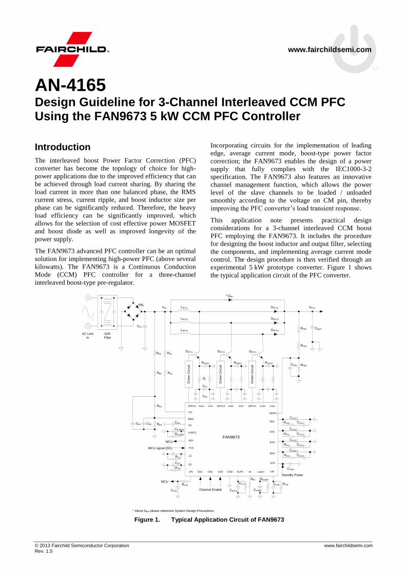
AN-4165 Design Guideline for 3-Channel Interleaved CCM PFC Using the FAN9673 5 kW CCM PFC Controller
Introduction
The interleaved boost Power Factor Correction (PFC)
converter has become the topology of choice for high-
power applications due to the improved efficiency that can
be achieved through load current sharing. By sharing the
load current in more than one balanced phase, the RMS
current stress, current ripple, and boost inductor size per
phase can be significantly reduced. Therefore, the heavy
load efficiency can be significantly improved, which
allows for the selection of cost effective power MOSFET
and boost diode as well as improved longevity of the
power supply.
The FAN9673 advanced PFC controller can be an optimal
solution for implementing high-power PFC (above several
kilowatts). The FAN9673 is a Continuous Conduction
Mode (CCM) PFC controller for a three-channel
interleaved boost-type pre-regulator.
Incorporating circuits for the implementation of leading
edge, average current mode, boost-type power factor
correction; the FAN9673 enables the design of a power
supply that fully complies with the IEC1000-3-2
specification. The FAN9673 also features an innovative
channel management function, which allows the power
level of the slave channels to be loaded / unloaded
smoothly according to the voltage on CM pin, thereby
improving the PFC converter’s load transient response.
This application note presents practical design
considerations for a 3-channel interleaved CCM boost
PFC employing the FAN9673. It includes the procedure
for designing the boost inductor and output filter, selecting
the components, and implementing average current mode
control. The design procedure is then verified through an
experimental 5 kW prototype converter. Figure 1 shows
the typical application circuit of the PFC converter.
LPFC1 DPFC1
CB+
RB1
RA1
RA2
LPFC2 DPFC2
LPFC3 DPFC3
VPFC
IEA1
SS
BIBO
CS1+
IAC
ILIMIT2
OPFC1
VDD
VIR
FBPFC
VEA CVC1RVC1
CVC2
CSS
CM1 CM2 CM3
CS1- CS2+ CS2- CS3+ CS3-
IEA2
IEA3
OPFC2 OPFC3
CVDD
FAN9673RILIMIT2
CILIMIT2
COUTRFB1
RFB2
RFB3CFB3
CVIR RVIR
CIC11RIC1
CIC12
CIC21RIC2
CVI22
CIC31RIC3
CIC32
SPFC1
RSEN1
Drive
r C
ircu
it
SPFC2
RSEN2
Drive
r C
ircu
it
SPFC3
RSEN3
Drive
r C
ircu
it
RF
CF1
CF2
RI
PVO
LPK
RDY
ILIMIT
RRI
MCU signal (DC)
MCU
CILIMIT
RILIMIT
RLPKGND
CRLPK
RRLPKMCU
CLPK
RLPK
CB2
RB1
RB2
RB4CB1
RB3
Channel Enable
GC
LS
RGC
CGC
RLS
VIN
Standby Power
AC Line
In
EMI
Filter
* DBP
* About DBP please reference System Design Precautions Figure 1. Typical Application Circuit of FAN9673

AN-4165
© 2013 Fairchild Semiconductor Corporation www.fairchildsemi.com Rev. 1.5 2
Design Procedure
In this section, a design procedure is presented using the
schematic of Figure 1 as the reference. A 5 kW rated
output power, three-channel CCM interleaved PFC with
universal input range is selected as a design example. The
design specifications are as follows:
Table 1. Design Specifications
Line Voltage Range 180~264 VAC PFC Output Voltage Ripple 5%
Line Frequency 50 Hz Switching Frequency fSW = 40 kHz
Nominal PFC Output Voltage VPFC = 393 V PFC Efficiency η > 0.95
Minimum PFC Output Voltage VPFC2 = 350 V Brownout Line Voltage 160 VAC
Output Power PO = 5 kW Brown-In Line Voltage 170 VAC
Number of Channel 3 Channel Management Method External Signal from MCU
[STEP-1] Estimate Input Rated Power and Output Current
The overall system is comprised of three parallel boost
PFC stages, as shown in Figure 2, so the input power of
the PFC stage is given as:
OUT TOT
IN
PP
(1)
where is the combined efficiency of the PFC stages.
The output current of PFC stage is given by:
-
OUT TOT
OUT TOT
PFC
PI
V
(2)
The output current of each boost stage is given by:
OUT TOT
OUT
PFC
PI
Channel NumberV
(3)
PIN
I OUT-TOT
POUT-TOT
VPFC
Boost PFCBoost PFC
Boost PFC
IOUT
Figure 2. PFC Stage Configuration
(Design Example)
-5000
52630.95
OUT TOT
IN
PP W
-5000
1667 3
OUT TOT
OUT
PP W
Channel Number
-
-
5000
39312.72OUT TOT
OUT TOT
PFC
PI A
V
-12.73
34.24OUT TOT
OUT
P
Channel NumberI A
[STEP-2] Frequency Setting
The internal oscillator frequency of the FAN9673 is
determined by the external resistor RRI on the RI pin. The
switching frequency is determined by the timing resistor
RRI, calculated as:
88 10SW
RI
fR
(4)
The guaranteed switching frequency ranges are
18 kHz~40 kHz and 55 kHz~75 kHz.
(Design Example) RRI of 20 k is selected to obtain
40 kHz switching frequency.
8 8
3
8 10 8 1020
40 10RI
SW
R kf
[STEP-3] VIN Range & RIAC Setting
The FAN9673 senses the peak value of line voltage using
the IAC pin, as shown in Figure 3. The peak value of the
line voltage is obtained by a peak detect circuit using a
sample-and-hold method. Meanwhile, the instantaneous
line voltage information is obtained by sensing the current
that flows into the IAC pin through RIAC.
RIAC should be selected according to the input voltage
range. For universal AC input (85 V~264 V), VVIR should
be set <1.5 V and RIAC should chosen as 6 MΩ. If the input
is high-voltage single-AC input (180 V~264 V), VVIR
should be set >3.5 V (maximum is 5 V) and RIAC should be
chosen as 12 MΩ. VVIR determines the application based
on the AC input range. The change of VVIR influences gain
of the gain modulator and the brown-in/out hysteresis.
85 ~ 265 6 , 1.5
180 ~ 265 12 , 3.5
AC IAC VIR
AC IAC VIR
V V V R M V V
V V V R M V V
(5)
The controller needs to set VVIR for the different input
range as:
VIR VIR VIRV I R (6)

AN-4165
© 2013 Fairchild Semiconductor Corporation www.fairchildsemi.com Rev. 1.5 3
IAC
LPK
Gain Modulator
RIAC
IIAC
VIN
IL
Peak
Detector
RCS
VEA
2.5V
VFBPFC
A (IAC)
B (VEA)
C (LPK)
A
C
B
VPFC
COUT
RFB1
RFB2
VFBPFC
Current Command
(C. Comd.)
Figure 3. Line Sensing Circuits
[STEP-4] PFC Inductor Design
The duty cycle of the boost switch at the peak of line
voltage is given as:
PFC
PFC
2 LINEL
V VD
V
(7)
Then, the maximum current ripple of the boost inductor at
the peak of minimum AC line voltage is given as:
2 2 1LINE MIN PFC LINE MINL
PFC PFC SW
V V VI
L V f
(8)
The average of boost inductor current over one switching
cycle at the peak of the line voltage for minimum AC input
is given by:
2 OUTL AVG
LINE MIN
PI
V
(9)
IL.L AVGI
.L AVGI
.
L
RF
L AVG
IK
I
.L PKI
Figure 4. Inductor Current
For a given current ripple factor (KRF=IL/ILAVG), the boost
inductor value can be obtained as:
2 2 1LINE MIN PFC LINE MINPFC
RF L AVG PFC SW
V V VL
K I V f
(10)
The maximum current of boost inductor is:
2(1 ) (1 )
2 2
OUTRF RFL PK L AVG
LINE MIN
PK KI I
V
(11)
[STEP-5] PFC Output Capacitor Selection
(1 cos(4 ))D AVG OUT TOT LINEI I f t
OUT TOTI
2
OUT TOTPFC RIPPLE
LINE OUT
IV
f C
PFCV
D AVGI
DI
Figure 5. PFC Output Voltage Ripple
The output voltage ripple should be considered when
selecting the PFC output capacitor. Figure 5 shows the line
frequency ripple on the output voltage. With a given
specification of output ripple, the value for the output
capacitor can be obtained from:
-
2
OUT TOTOUT
LINE PFC RIPPLE
IC
f V
(12)
where IOUT is nominal output current of the boost PFC
stage and VPFC-RIPPLE is the peak-to-peak output
voltage ripple.
(Design Example) The PFC is designed for high-voltage
single-AC input (180 V~264 V). RIAC should be chosen as
12 MΩ and RVIR is:
10 470 4.7 >3.5VIR VIR VIRV I R A k V V
470 k is selected as RVIR for the AC input range of
180 V~264 V.
(Design Example) The average of the boost inductor
current over one switching cycle at the peak of the
minimum AC line (assume it’s brownout of PFC) is
obtained as:
2 2 166715.5
160 0.95
OUTL AVG
LINE MIN
PI A
V
The boost inductor is obtained as:
3
2 2 1
2 160 393 2 160 1100
1.55 15.5 393 40 10
LINE MIN PFC LINE MINPFC
RF L AVG PFC SW
V V VL
K I V f
H
The maximum current of the boost inductor is given as:
2(1 )
2
2 1667 1.55(1 ) 27.51
160 0.95 2
OUT RFL PK
LINE MIN
P KI
V
A

AN-4165
© 2013 Fairchild Semiconductor Corporation www.fairchildsemi.com Rev. 1.5 4
The hold-up time should also be considered when
determining the output capacitor value:
-
2 2
2 OUT TOT HOLDOUT
PFC PFC MIN
P tC
V V
(13)
where POUT-TOT is nominal output power of boost PFC
stage; tHOLD is the required holdup time; and VPFC-MIN is
the allowable minimum PFC output voltage during the
hold-up time.
[STEP-6] Output Sensing & PVO Setting
To improve system efficiency, the FAN9673 incorporates
the programmable PFC output voltage function (PVO). As
shown in Figure 6, when the PFC output voltage is much
higher than the peak voltage of the AC input, the user can
input a DC level from the MCU to the PVO pin to
decrease the PFC output voltage. (It is recommended that
the PFC output voltage is set at least 25 V higher than the
peak voltage of AC input. Otherwise, it is necessary to
consider other factors closely related to the PFC output
voltage regulation, such as hold-up time, PF, and THD
standard of input current.)
The relationship between the feedback voltage level for the
PFC output voltage and VPVO is given as:
4
PVO
FBPFC REF
VV V (14)
Once the desired PFC output voltage, VPFC2, for low AC
input is determined; the required DC voltage level VPVO is
given by:
3
2
1 2 3
4 ( )FB
PVO REF PFC
FB FB FB
RV V V
R R R
(15)
RFB2
RFB3
FBPFC
VPFC
VO
VFBPFC
2.25V
2.5V
354V
393V
PVO
IL
RCS
2.5V
gmv
External
Signal
(MCU)
Voltage Protection
1V
0V
VPVOVFBPFC
RFB1
Figure 6. Two-Level PFC Output Block
[STEP-7] Current-Sensing & Current-Limit
IEA
VIN
IMO
OPFC
FBPFCRFB3
VPFC
RI
IL
RCS
Drive
Logic
OSC
CS+
IAC
VEA
RIAC
CV2
CV1
RV1
PVO
CMCM
RM
gmi
gmv
RFB1+FB2
LS
CI2
CI1
RI1
LPK Peak
Detecter
LPT
2.5V
CS-
Figure 7. PFC Compensation Circuits
(Design Example) With peak-to-peak voltage ripple
specification of 5% of VPFC, the capacitor should be:
-
2
12.722060
2 50 (393 5%)
OUT TOTOUT
LINE PFC RIPPLE
IC
f V
F
Since the minimum allowable output voltage during one
cycle (15 ms) drop-out is 300 V, the capacitor value
should be:
In this case, three parallel connected capacitors of 680 F
are selected for the PFC output capacitor. In this design
example, the target application for the three-channel PFC
is a home appliance power supply, so there is no hold-up
time requirement.
(Design Example) Set the PFC output level at 393 V,
RFB3=23.7 k:
3
1 2
3
( )
23.7 10 (393 2.5)3.7
2.5
FB PFC REF
FB FB
REF
R V VR R
V
M
Set VPFC2 =350 V for low input AC 200 V, the required
VPVO is then:
3
2
1 2 3
3
6 3
4 ( )
23.7 104 2.5 350( ) 1.09
3.7 10 23.7 10
FB
PVO REF PFC
FB FB FB
RV V V
R R R
V
The PVO function is used to change the output voltage
of PFC,VPFC, which should be kept at least 25 V higher
than VIN.
3-
2 2 2 2
2 2 5000 15 102327
393 300
OUT TOT HOLDOUT
PFC PFC MIN
P tC F
V V

AN-4165
© 2013 Fairchild Semiconductor Corporation www.fairchildsemi.com Rev. 1.5 5
Figure 7 shows the PFC compensation circuits. The first
step in compensation network design is to select the
current-sensing resistor of the PFC converter, considering
the control window of voltage loop. Since line feed-
forward is used in FAN9673, the output power is
proportional to the output of voltage control error amplifier,
VVEA, as shown below:
0.6( )
0.6
VEA
OUT VEA OUT MAX
VEA SAT
VP V P
V
(16)
The maximum power limit of PFC is:
2
LINE MIN MAX M
OUT MAX
IAC CS
V G RP
R R
(17)
The RM is the output resistor of for multiplier to transfer
the current command to a voltage type signal. GMAX is a
coefficient of the internal control loop.
VCSPFC
Command
Gmi+
VCS.PK
VILIMIT/4
VILIMIT2 = Saturation Protection
Case1:
Max. Power (Normal),
VVEA-MAX“B”= 6V
Case2:
>Max. Power (Abnormal),
AC cycle drop
VVEA = 6V, but“C”abnormal
short time, clamp by VILIMIT
Case3:
>Max. Power (Abnormal),
AC cycle drop, as left case,
but user uses wrong choke
can not afford current at
Max. command.
Right design,
max power
limited by
VVEA
Right design at
abnormal test,
command from
Multiplier clamp
by VILIMIT
Wrong design at
abnormal test, but
protect by VILIMIT2
Non-SaturationVILIMIT2
Figure 8. ILIMIT and ILIMIT2 Function
The FAN9673 has three cases of current limit protections
via the VEA, ILIMIT, and ILIMIT2 to protect OCP and inductor
saturation. The user can program the current limit threshold
VILIMIT1 and VILIMIT2 by resistor.
Case 1, power (normal state): In the normal case, current /
power should be controlled by a command, VM, from the
gain modulator. When VVEA rises to 6 V, the output power
and current of the system are at peak. The power and current
can’t increase further.
Case 2, current limit 1 (abnormal state): The current
command from the gain modulator is k*IAC*VVEA/VLPK2.
When the system works in abnormal state, such as when the
AC cycle is missed and returns in a short period, the VLPK
has a delay before returning to the original level. This delay
significantly increases the current command. If the
command is greater than the ILIMIT clamp level VILIMIT, it is
limited as in Case 2, shown in Figure 8. If the inductor
current is not saturated, the peak current of this state can be
the maximum current design for each channel.
Case 3, current limit 2 (saturation state): In case 3, use
the level 80%~90% of maximum current of the switch
device to be the saturation protection. This current
protection is cycle–by-cycle limited.
RI5
ILIMIT3
1.2V
A
C
B
Gain Modulator
I
RILIMITI*RILIMIT
VX4
1/4
Figure 9. Internal Block of ILIMIT
ILIMIT should be triggered before ILIMIT2, because ILIMIT2 is
used to prevent saturation of the inductor from damaging
switches. ILIMIT signal limits the maximum power /current
by clamping level VILIMIT. VILIMIT is set by the external
resistor RILIMIT.
It is typical to set the maximum power limit of the PFC
stage to around 120%~150% of full load, such that the
VVEA is around 4~4.5 V.
Resistor RILIMIT can be calculated from:
1.8 ( / 3) 2 4IN CSILIMIT
LINE MIN ILIMIT
P RR
V I
(18)
Regarding the choice for ILIMIT2 level, the user can use
150% of maximum power as the setting. It’s used to
protect the switching devices. User can also use the
maximum current rating of the semiconductor device with
10% to 20% de-rating as the limit level. ILIMIT2 setting is
obtained as:
2
2
150% CS PKILIMIT
ILIMIT
VR
I
(19)
(Design Example) Setting the maximum power limit of
each PFC stage as 2.167 kW (130% of full load per
channel), the current sensing resistor is obtained from:
2 2 3
6
160 2 7.5 100.0147
12 10 1.3 1667
LINE MIN MAX M
CS
IAC OUT MAX
V G RR
R P
A 15 m resistor is selected.
(Design Example) 0.015 27.51 0.413CS PK CS L PKV R I V
fSW=40 kHz, is selected, IILIMIT2 and IILIMIT is:
-5
3
1.2 1.0208 1.2256.13 10
20 10ILIMIT
RI
I AR
-5
2 3
1.2 1.03125 1.23756.19 10
20 10ILIMIT
RI
I AR
2 -5
2
150% 1.5 0.41310
6.19 10
CS PKILIMIT
ILIMIT
VR k
I
A 10 kΩ resistor is selected for ILIMIT2.
The setting of ILIMIT is obtained as:
-5
1.8 ( / 3) 2 4
1.8 1754 2 0.015 427.3
160 6.13 10
IN CSILIMIT
LINE MIN ILIMIT
P RR
V I
k
A 30 kΩ resistor is selected for ILIMIT.

AN-4165
© 2013 Fairchild Semiconductor Corporation www.fairchildsemi.com Rev. 1.5 6
[STEP-8] LS & GC Design
tON tOFF
IL
Figure 10. LPT Function for Inductor Current at tOFF
The Linear Predict (LPT) function, shown in Figure 10, is
used to anticipate the behavior of inductor current in the
switch turn-off region. The Gain Change (GC) pin and LS
pin are used to adjust the parameters of LPT function. The
resistance can be determined by the following equation.
3
32191051FB
FBFBFBCS
-
PFCLS
R
RRRR.
L R
(20)
Gain change is to use to adjust the output of the gain
modulation. The resistor value is given by:
3
321
6106
FB
FBFBFB
GC
R
RRRR
(21)
[STEP-9] PFC Current Loop Design
The transfer function that relates the duty cycle to the
inductor current of boost power stage is given as:
PFCL
PFC
Vi
sLd (22)
The transfer function relating the output of the current
control error amplifier to the inductor current-sensing
voltage is obtained by:
1CS CS PFC
IEA RAMP PFC
v R V
v V sL
(23)
where VRAMP is the peak-to-peak voltage of the ramp
signal for the current-control PWM comparator, which
is 3.8 V.
The transfer function of the compensation circuit is given as:
12 2
12
IEA II IZ
CS
IP
s
v f f
sv s
f
(24)
where:
1 1
2
1,
2 2
1
2
MIII IZ
IC IC IC
IP
IC IC
Gf f and
C R C
fR C
(25)
The procedure to design the feedback loop is as follows:
(a) Determine the crossover frequency (fIC) around
1/10th
~1/6th
of the switching frequency. Then calculate
the gain of the transfer function of Equation (26) at
crossover frequency as:
@2
IC
CS CS PFC
IEA RAMP IC PFCf f
v R V
v V f L
(26)
(b) Calculate RIC such that it makes the closed loop gain
unity at crossover frequency:
@
1
IC
IC
CSMI
IEA f f
Rv
Gv
(27)
(c) Since the control-to-output transfer function of the
power stage has -20 dB/dec slope and -90o phase at
the crossover frequency of 0 dB, as shown in Figure
11, it is necessary to place the zero of the
compensation network (fIZ) around on third (1/3) of
the crossover frequency so that more than 45 phase
margin is obtained. Then the capacitor CIC1 is
determined as:
1
1
2 / 3IC
IC IC
CR f
(28)
40dB
20dB
0dB
-20dB
-40dB
10Hz 100Hz 1kHz 10kHz 100kHz
fIZ
Control-to-output
1MHz
fIC
Compensation
Closed Loop Gain60dB
fIP
Figure 11. Current Loop Compensation
(d) Place compensator high-frequency pole (fCP) at least a
decade higher than fIC to ensure that it does not
interfere with the phase margin of the current loop at
its crossover frequency.
2
1
2IC
IP IC
Cf R
(29)
(Design Example) Inductance of 220 μH is selected.
RLS and RGC are obtained as:
-9 1 2 3
3
-6
6 3-9
3
1.5 10
100 10 28.2
3.7 10 23.7 101.5 10 0.015
23.7 10
LS
FB FB FBCS
FB
LR
R R RR
R
k
6 6
6 3
1 2 3
3
3
6 10 6 1038.19
3.7 10 23.7 10
23.7 10
GC
FB FB FB
FB
R kR R R
R
RLS and RGC are 33 kΩ and 38.2 kΩ used.

AN-4165
© 2013 Fairchild Semiconductor Corporation www.fairchildsemi.com Rev. 1.5 7
[STEP-10] PFC Voltage Loop Design
Since FAN9673 employs line feed-forward, the power
stage transfer function becomes independent of the line
voltage. Then, the low-frequency, small-signal, control-to-
output transfer function is obtained as:
ˆ 1
ˆ 5
PFC OUT TOT MAX
VEA OUT
v I K
v sC
(30)
where /MAX
MAX OUT OUTK P P and 5 V is the control
window of error amplifier (5.6 V-0.6 V=5 V)
40dB
20dB
0dB
-20dB
-40dB
1Hz 10Hz 100Hz 1kHz
Control-to-Output
10kHz
60dB
fc
Compensation
Closed-Loop Gain
Figure 12. Voltage Loop Compensation
Proportional and integration (PI) control with high-
frequency pole typically used for compensation. The
compensation zero (fVZ) introduces phase boost, while the
high-frequency compensation pole S(fVP) attenuates the
switching ripple, as shown in Figure 12.
The transfer function of the compensation network is
obtained as:
1ˆ 2 2
ˆ1
2
COMP VI VZ
PFC
VP
s
v f f
sv s
f
(31)
where:
1 1
2
2.5 1,
2 2
1
2
MVVI VZ
OUT VC VC VC
VP
VC VC
Gf f and
V C R C
fR C
(32)
The procedure to design the feedback loop is as follows:
(a) Determine the crossover frequency (fVC) around
1/10~1/5 of the line frequency. Since the control-to-
output transfer function of power stage has -20 dB/dec
slope and -90o phase at the crossover frequency, shown
in Figure 12 as 0 dB; it is necessary to place the zero of
the compensation network (fVZ) around the crossover
frequency so that 45 phase margin is obtained. Then,
the capacitor CVC1 is determined as:
1 2
2.5
5 (2 )
MV OUT TOT MAXVC
PFCOUT VC
G I KC
VC f
(33)
To place the compensation zero at the crossover frequency,
the compensation resistor is obtained as:
1
1
2VC
VC VC
Rf C
(34)
(b) Place compensator high-frequency pole (fVP) at least a
decade higher than fC to ensure that it does not interfere
with the phase margin of the voltage regulation loop at
its crossover frequency. It should also be sufficiently
lower than the switching frequency of the converter so
noise can be effectively attenuated. Then, the capacitor
CVC2 is determined as:
2
1
2VC
VP VC
Cf R
(35)
(Design Example)
Set the crossover frequency as 20 Hz:
-1 2
6
6 2
2.5
5 (2 )
70 10 12.72 1.3 2.546
10 3935 2040 (2 20)
MV OUT TOT MAXVC
PFCOUT VC
G I KC
VC f
nF
Modify the DC gain and BW of voltage loop; using 75 kΩ
for RVC, 1 F for CVC1, and 0.1 F for CVC2.
9
1
1 1173
2 2 20 46 10VC
VC VC
R kf C
2 3
1 19.2
2 2 100 173 10VC
VP VC
C nFf R
(Design Example) Set crossover frequency as 4 kHz:
@
3 6
2
0.015 3930.469
(6.5-1.5) 2 4 10 100 10
IC
CS CS PFC
IEA RAMP IC PFCf f
v R V
v V f L
6
@
1 124.2
88 10 0.469
IC
IC
CSMI
IEA f f
R kv
Gv
1 3 3
1 14.93
2 / 3 24.2 10 2 4 10 / 3IC
IC IC
C nFR f
2 4 3
1 10.16
2 2 4 10 24.2 10IC
IP IC
C nFf R
Modify the DC gain and BW of current loop, use 17.4 kΩ
for RIC, 2.2nF for CIC1, and 100 pF for CIC2.

AN-4165
© 2013 Fairchild Semiconductor Corporation www.fairchildsemi.com Rev. 1.5 8
[STEP-11] Channel Management Control
Figure 13 shows the CM pin control with an external voltage
signal. The VVEA control voltage is generated by regulation
error amplifier and is proportional to average current of
input. When VCM is pulled LOW to 0 V, the PFC channel
is enabled. When the VCM is pulled HIGH and over 4 V,
the channel is disabled. Figure 14 shows that channel 3 is
disabled by an external signal when the system is operating
at half-load condition.
1000
V (V)
6
VCVM
IL
VAC
VCVM-LIMIT (4V)
VVEA
Figure 13. Channel Management by MCU
0˚ 120˚ 240˚
120˚à 180˚
IL1
IL2
IL3
IL1
IL2
IL3
Full load, all channel operation
Mid. load, disable channel 3 by external signal
Figure 14. Phase Change of External Signal Control
The Figure 16 shows an external circuit used to change the
slope of VCM2/3. When VCM2/3 is between 4 V ~ 0 V, changing
the slope of VCM2/3 can increase / decrease the loading of the
channel and decrease the overshoot/undershoot of the PFC
output voltage, as the Figure 15 shows. This method
significantly improves the dynamic load performance of the
PFC converter.
CM2 /3
C=470pF
R=5k~10kΩ
VCM2 /3
Figure 15. Channel Management by MCU
IL1
VCM
VAC
IL2
PO
VO
IL1
VAC
IL2
VO
VCM
Direct
Indirect
VS
4V
4V
Figure 16. Channel Management by MCU
[STEP-12] Soft Start
Figure 17 shows the soft start (SS) waveform. FAN9673 uses
soft-start voltage, VSS, to clamp the PFC power command of
voltage loop VVEA. To increase the soft-start time, the value of
the soft-start capacitance CSS can be increased.
SS SS
SS
SS
I tC
V
(36)
(Design Example) Assuming that VVEA is out of clamping by VSS at 5 V, the
design soft-start time tSS is 50 ms and ISS is 20 μA. The
required soft-start capacitor value is:
6 3I t 20 10 100 10C 0.4 F
V 5
SS SS
SS
SS
0.47 F is selected for CSS.
IL
VFBPFC
VSS
PFC Soft Start
VAC
VVEA
VREF
Figure 17. Soft-Start Waveform
AN-4165
© 2013 Fairchild Semiconductor Corporation www.fairchildsemi.com Rev. 1.5 9
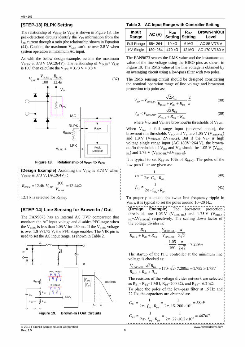
[STEP-13] RLPK Setting
The relationship of VIN.PK to VLPK is shown in Figure 18. The
peak-detection circuits identify the VIN information from the
IAC current through a ratio (the relationship shown in Equation
(41). Caution: the maximum VLPK can’t be over 3.8 V when
system operation at maximum AC input.
As with the below design example, assume the maximum
VIN.PK at 373 V (AC264V). The relationship of VIN.PK / VLPK
is 100, then calculate the VLPK = 3.73 V < 3.8 V.
.
100 12.4
IN PK RLPK
LPK
V RV
k
(37)
Peak
Detector
Ratio
IAC
RIAC
LPK
RLPK
VLPK
VIN
RRLPK
Figure 18. Relationship of VIN.PK to VLPK
[STEP-14] Line Sensing for Brown-In / Out
The FAN9673 has an internal AC UVP comparator that
monitors the AC input voltage and disables PFC stage when
the VBIBO is less than 1.05 V for 450 ms. If the VBIBO voltage
is over 1.9 V/1.75 V, the PFC stage enables. The VIR pin is
used to set the AC input range, as shown in Table 2.
BIBO
RB1+2
RB3
RB4
CB1
CB2
120/100Hz
fp1 fp2
RMS
IN
V
V
VIN
PFC Action
PFC Stop
Figure 19. Brown-In / Out Circuits
Table 2. AC Input Range with Controller Setting
Input Range
AC (V) RVIR
Setting RIAC
Setting Brown-In/Out
Level
Full-Range 85~ 264 10 kΩ 6 MΩ AC 85 V/75 V
HV-Single 180~264 470 kΩ 12 MΩ AC 170 V/160 V
The FAN9673 senses the RMS value and the instantaneous
value of the line voltage using the BIBO pins as shown in
Figure 19. The RMS value of the line voltage is obtained by
an averaging circuit using a low-pass filter with two poles.
The RMS sensing circuit should be designed considering
the nominal operation range of line voltage and brownout
protection trip point as:
4
.
1 2 3 4
2 2B
BO LINE BO
B B B
RV V
R R R
(38)
4
.
1 2 3 4
2 B
BI LINE MIN
B B B
RV V
R R R
(39)
where VBO and VBI are brownout/in thresholds of VRMS.
When VAC is full range input (universal input), the
brownout / in thresholds VBO and VBI are 1.05 V (VBIBO-FL)
and 1.9 V (VBIBO-FL+∆VBIBO-F). But if the VAC is high
voltage single range input (AC 180V~264 V), the brown-
out/in thresholds of VBO and VBI should be 1.05 V (VBIBO-
HL) and 1.75 V (VBIBO-HL+∆VBIBO-H).
It is typical to set RB3 as 10% of RRB+2. The poles of the
low-pass filter are given as:
1
1 3
1
2P
B B
fC R
(40)
2
2 4
1
2P
B B
fC R
(41)
To properly attenuate the twice line frequency ripple in
VRMS, it is typical to set the poles around 10~20 Hz.
(Design Example) The brownout protection
thresholds are 1.05 V (VBIBO-HL) and 1.75 V (VBIBO-
HL+∆VBIBO-H) respectively. The scaling down factor of
the voltage divider is:
4
1 2 3 4 . 2 2
1.057.289
160 2 2
BIBO HLB
B B B LINE BO
VR
R R R V
m
The startup of the PFC controller at the minimum line
voltage is checked as:
. 4
1 2 3 4
2170 2 7.289 1.752 1.75LINE MIN B
B B B
V Rm V
R R R
The resistors of the voltage divider network are selected
as RB1= RB2=1 M, RB3=200 k, and RB4=16.2 k.
To place the poles of the low-pass filter at 15 Hz and
22 Hz, the capacitors are obtained as:
1 3
1 3
1 153
2 2 15 200 10B
P B
C nFf R
2 3
2 4
1 1447
2 2 22 16.2 10B
P B
C nFf R
(Design Example) Assuming the VLPK is 3.73 V when
VIN.PK is 373 V, (AC264V) :
.
10012.4 12.4RLPK LPK
IN PK
R k V kV
12.1 k is selected for RRLPK.

AN-4165
© 2013 Fairchild Semiconductor Corporation www.fairchildsemi.com Rev. 1.5 10
Design Summary
Application Output Power Input Voltage Output Voltage / Output Current
Single-Stage Three-Channel PFC 5000 W 180~264 VAC 393 V/12.72 A
Features
AC180V~264 V, Three-Channel PFC Using FAN9673
Switch-Charge Technique of Gain Modulator for Better PF and Lower THD
40 kHz Low Switching Frequency Operation with IGBT
Protections: Over-Voltage Protection (OVP), Under-Voltage Protection (UVP), and Over-Current Protection (ILIMIT),
Inductor Saturation Protection (ILIMIT2)
SPFC1~3
CB
Rsen1
RB1
VPFC
IEA1
RI
SS
LPK
CS1-
IAC
ILIMIT2
GND
OPFC1
VIR
VDD
FBPFC
VEACVC1RVC1
CVC2
CSS
PVOCM1 CM2 CM3
CS1+ CS2- CS2+ CS3- CS3+
IEA2
IEA3
LS
GC
RDY ILIMIT
OPFC2 OPFC3
FAN9673
RILIMIT2
CILIMIT2
RRI
MCU signal
(DC)
COUTRFB1
RFB3CFB
CVDD
RVIR
CVIR
MCU/
Sec. Stage
(PFC Ready)
15mΩ
FGH40N60SMDF
1µF 2040μF2.2MΩ
23.7kΩ470pF
100nF
75kΩ 1µF
CIC11RIC11
CIC12 100pF
17.4kΩ 1nF
CIC21RIC21
CIC122 100pF
17.4kΩ 1nF
CIC31RIC31
CIC32 100pF
17.4kΩ 1nF
22μF
1nF
470kΩ
20kΩ
0.1µF
0.47µF
10kΩ
10nF
470ΩRF1~2
2.2nFCF1
CB2
BIBO
RB1
RB2
RA1
RA2
1MΩ
1MΩ
6MΩ
6MΩ
RB4
16.2kΩ
0.47μF
RFB2
1.5MΩ
VDD
Rsen2
15mΩ
VDD
Rsen3
15mΩ
VDD
2.2nF
CF2
LPFC1 DPFC1
FFH30S60STU100µH
LPFC2
100µH
LPFC3
100µH
DPFC2
FFH30S60STU
DPFC3
FFH30S60STU
RLPK
RLPK
CRLPK
12.1kΩ
10nF
CB1
47nF
RB3
200kΩ
RGC
CGC
38.2kΩ
470pF
RLS
CLS
43kΩ
470pF
MCU
CLPK
RLPK
4.7kΩ
RILIMITCILIMIT
30kΩ10nF
DC Setting Level
Standby
Power
* DBP1, 2
1N5406
Figure 20. Final Schematic of Design Example

AN-4165
© 2013 Fairchild Semiconductor Corporation www.fairchildsemi.com Rev. 1.5 11
Appendix A
Table 3. Parameters of FAN9673 Evaluation Board
VDD Maximum Rating 20 V
VDD OVP 24 V
VCC UVLO 10.3 V/12.8 V
PVO 0 V~1 V
PFC Soft-Start CSS = 0.47 µF
Brown-In/Out 170 V/160 V
Gate Clamp 2.4 V/1.55 V (96%/62%)
VDD Maximum Rating 20 V
Table 4. MOSFET and Diode Reference Specification
IGBTs
Voltage Rating
600 V (IGBT) FGH40N60SMDF
Boost Diodes
600 V FFH30S60STU
System Design Precautions
Pay attention to the inrush current when AC input is first connected to the boost PFC convertor. It is recommended to
use NTC and a parallel connected relay circuit to reduce inrush current.
Add bypass diode DBP to provide a path for inrush current when PFC starts up.
The PFC stage is normally used to provide power to a downstream DC-DC or inverter. It’s recommend that
downstream power stage is enabled to operate at full load once the PFC output voltage has reaches a level close to the
specified steady-state value.
The PVO function is used to change the output voltage of PFC, VPFC. The VPFC should be kept at least 25 V higher
than VIN.

AN-4165
© 2013 Fairchild Semiconductor Corporation www.fairchildsemi.com Rev. 1.5 12
Layout Guide
The current-sense resistor and current-sense filter
(CF1, CF2) should be as close to the CS+/CS- pins
as possible.
Similar to other power management devices, when
laying out the PCB, it is important to use star
grounding techniques and to keep the filter capacitor
and control components as close to the controller IC
and its GND pin as possible.
Keep high-current output and power ground paths
separate from the signal ground path. Make a single-
point connection from signal ground to the power
ground. Connect the FAN9673’s GND to the power
ground at the negative terminal of COUT.
The ground of power stage and controller stage only
meet at the negative terminal of the output capacitor,
COUT. The return path for the gate drive current should
be connected to the power ground. Minimize the
ground loops between the driver outputs, totem-pole
buffer transistors, power switches, and power ground.
Keep the controller as close to the switching devices
as possible to minimize the length and loop inductance
of the high-current gate driving traces.
To minimize the possibility of interference caused by
magnetic coupling from the boost inductor, the device
should be located at least 2.5 cm (1 inch) away from the
boost inductor. It is also recommended that the device
not be placed underneath magnetic components.
Keep the width of PCB track handling the gate drive
current to the switching devices wide to handle the
high peak current level.
SPFC1~3
CB
Rsen1
RB1
VPFC
COUTRFB1
RFB3CFB
CF1
CB2
RB1
RB2
RA1
RA2
RB4
RFB2
VDD
Rsen2
VDD
Rsen3
VDD
LPFC1 DPFC1
LPFC2
LPFC3
DPFC2
DPFC3
CB1
RB3
IEA1
RI
SS
LPK
CS1-
IAC
ILIMIT
GND
OPFC1
VIR
VDD
FBPFC
VEA CVC1RVC1
CVC2
CSS
PVOCM1 CM2 CM3
CS1+ CS2- CS2+ CS3- CS3+
IEA2
IEA3LS
GC
RDY OPP
OPFC2 OPFC3
FAN9673
RILIMIT
CILIMIT
RRI ROPP
MCU signal
(DC)
CVDD
VDD
RVIR
CVIR
MCU/
Sec. Stage
(PFC Ready)
MCU
(Input Information)
CLPK
CIC11RIC11
CIC12
CIC21RIC21
CIC122
CIC31RIC31
CIC32
BIBO
DC Setting Level
RLPK
RLPK
CRLPK
RGC
CGC
RLS
CLS
3
2
4
5
1
CF2
DBP
Figure 21. Layout Diagram
AN-4165
© 2013 Fairchild Semiconductor Corporation www.fairchildsemi.com Rev. 1.5 13
Related Product Information
FAN9673 — Three Channels Interleaved CCM PFC Controller
FAN6982 — CCM Power Factor Correction Controller
AN-8027 — FAN480X PFC+PWM Combo Controller Application
DISCLAIMER FAIRCHILD SEMICONDUCTOR RESERVES THE RIGHT TO MAKE CHANGES WITHOUT FURTHER NOTICE TO ANY PRODUCTS HEREIN TO IMPROVE RELIABILITY, FUNCTION, OR DESIGN. FAIRCHILD DOES NOT ASSUME ANY LIABILITY ARISING OUT OF THE APPLICATION OR USE OF ANY PRODUCT OR CIRCUIT DESCRIBED HEREIN; NEITHER DOES IT CONVEY ANY LICENSE UNDER ITS PATENT RIGHTS, NOR THE RIGHTS OF OTHERS.
LIFE SUPPORT POLICY FAIRCHILD’S PRODUCTS ARE NOT AUTHORIZED FOR USE AS CRITICAL COMPONENTS IN LIFE SUPPORT DEVICES OR SYSTEMS WITHOUT THE EXPRESS WRITTEN APPROVAL OF THE PRESIDENT OF FAIRCHILD SEMICONDUCTOR CORPORATION. As used herein:
1. Life support devices or systems are devices or systems which, (a) are intended for surgical implant into the body, or (b) support or sustain life, or (c) whose failure to perform when properly used in accordance with instructions for use provided in the labeling, can be reasonably expected to result in significant injury to the user.
2. A critical component is any component of a life support device or system whose failure to perform can be reasonably expected to cause the failure of the life support device or system, or to affect its safety or effectiveness.

www.onsemi.com1
ON Semiconductor and are trademarks of Semiconductor Components Industries, LLC dba ON Semiconductor or its subsidiaries in the United States and/or other countries.ON Semiconductor owns the rights to a number of patents, trademarks, copyrights, trade secrets, and other intellectual property. A listing of ON Semiconductor’s product/patentcoverage may be accessed at www.onsemi.com/site/pdf/Patent−Marking.pdf. ON Semiconductor reserves the right to make changes without further notice to any products herein.ON Semiconductor makes no warranty, representation or guarantee regarding the suitability of its products for any particular purpose, nor does ON Semiconductor assume any liabilityarising out of the application or use of any product or circuit, and specifically disclaims any and all liability, including without limitation special, consequential or incidental damages.Buyer is responsible for its products and applications using ON Semiconductor products, including compliance with all laws, regulations and safety requirements or standards,regardless of any support or applications information provided by ON Semiconductor. “Typical” parameters which may be provided in ON Semiconductor data sheets and/orspecifications can and do vary in different applications and actual performance may vary over time. All operating parameters, including “Typicals” must be validated for each customerapplication by customer’s technical experts. ON Semiconductor does not convey any license under its patent rights nor the rights of others. ON Semiconductor products are notdesigned, intended, or authorized for use as a critical component in life support systems or any FDA Class 3 medical devices or medical devices with a same or similar classificationin a foreign jurisdiction or any devices intended for implantation in the human body. Should Buyer purchase or use ON Semiconductor products for any such unintended or unauthorizedapplication, Buyer shall indemnify and hold ON Semiconductor and its officers, employees, subsidiaries, affiliates, and distributors harmless against all claims, costs, damages, andexpenses, and reasonable attorney fees arising out of, directly or indirectly, any claim of personal injury or death associated with such unintended or unauthorized use, even if suchclaim alleges that ON Semiconductor was negligent regarding the design or manufacture of the part. ON Semiconductor is an Equal Opportunity/Affirmative Action Employer. Thisliterature is subject to all applicable copyright laws and is not for resale in any manner.
PUBLICATION ORDERING INFORMATIONN. American Technical Support: 800−282−9855 Toll FreeUSA/Canada
Europe, Middle East and Africa Technical Support:Phone: 421 33 790 2910
Japan Customer Focus CenterPhone: 81−3−5817−1050
www.onsemi.com
LITERATURE FULFILLMENT:Literature Distribution Center for ON Semiconductor19521 E. 32nd Pkwy, Aurora, Colorado 80011 USAPhone: 303−675−2175 or 800−344−3860 Toll Free USA/CanadaFax: 303−675−2176 or 800−344−3867 Toll Free USA/CanadaEmail: [email protected]
ON Semiconductor Website: www.onsemi.com
Order Literature: http://www.onsemi.com/orderlit
For additional information, please contact your localSales Representative
© Semiconductor Components Industries, LLC