Embed Size (px)
Citation preview
INV ITEDP A P E R
Inorganic Materials andAssembly Techniquesfor Flexible andStretchable ElectronicsImportant progress has been made in developing design strategies, materials,
and associated assembly techniques that provide approaches to electronics
with unconventional formats.
By Junwen He, Ralph G. Nuzzo, and John A. Rogers
ABSTRACT | In recent years, important progress has been
made in developing design strategies, materials, and asso-
ciated assembly techniques that provide empowering ap-
proaches to electronics with unconventional formats, ones
that allow useful but previously hard to realize attributes of
function. Notable examples of the progress made include: light
weight, large area, high performance electronics, optics, and
photonics; electronic and optical systems with curvilinear
shapes and capacities for accommodating demanding forms
of mechanical flexure; new device form factors for use in sens-
ing and imaging; the integration of high performance electron-
ics in 3-D with demanding nanometer design rules; functional
bioresponsive electronics; and advanced hybrid materials sys-
tems for lighting, energy storage, and photovoltaic energy
conversion. In this report we highlight advances that are ena-
bling such promising capabilities in technologyVspecifically,
the fabrication of device elements using high performance
inorganic electronic materials joined with printing and transfer
methods to effect their integration within functional modules.
We emphasize in this review considerations of the design
strategies and assembly techniques that, when taken together,
circumvent limitations imposed by approaches that integrate
circuit elements within compact, rigid, and essentially planar
form factor devices, and provide a transformational set of
capabilities for high performance flexible/stretchable
electronics.
KEYWORDS | Bio-integrated electronics; flexible electronics;
inorganic materials; integrated systems; stretchable electron-
ics; transfer printing
I . INTRODUCTION
The fabrication of high performance integrated circuits
provides examples of the most sophisticated manufactur-ing methods, as well as the most high-performance mate-
rials, used in any area of modern technology. The advanced
functional systems they provide are ones that are generally
characterized by a massive integration of circuit elements
within compact, rigid and essentially planar form factor
devices. The models of biology offer interesting points of
comparisonVones where system elements are integrated
with challenging 3-D design rules embedding materialsstructures that are frequently soft, curvilinear, and highly
flexural in their functional form. It represents an interest-
ing challenge in technology to develop strategies through
which existing classes of electronic materials (EMs)Vones
affording capabilities for high-circuit-level performanceVmight be utilized in conceptually related ways to provide
new functional capabilities. The envisioned uses include
electronic technologies permitting intimate integrationwith biological tissues, new capabilities for measurement
and sensing, efficient low-cost systems for energy transfor-
mation and storage, and perhaps most importantly modes
Manuscript received October 18, 2014; revised December 18, 2014; accepted
January 18, 2015. Date of current version May 19, 2015.
J. He is with the Department of Chemistry, University of Illinois at Urbana-Champaign,
Urbana, IL 61801 USA (e-mail: [email protected]).
R. G. Nuzzo and J. A. Rogers are with the Department of Materials Science and
Engineering, Department of Chemistry, University of Illinois at Urbana-Champaign,
Urbana, IL 61801 USA (e-mail: [email protected]; [email protected]).
Digital Object Identifier: 10.1109/JPROC.2015.2396991
0018-9219 � 2015 IEEE. Personal use is permitted, but republication/redistribution requires IEEE permission.See http://www.ieee.org/publications_standards/publications/rights/index.html for more information.
Vol. 103, No. 4, April 2015 | Proceedings of the IEEE 619
of large-area-integration for applications not countenancedby Moore’s law [1]. Exemplary cases here include: electro-
nic skins [2] and medical devices [3] that provide advanced
human-machine interfaces; bio-inspired cameras [5], [6]
embedding nonplanar/curvilinear electrooptics; wearable
electronic systems [7]; deformable displays [8]; and con-
formal mechanical energy harvesters [9]. One critical re-
quirement for all technologies of this type is the ability to
accommodate extremes in mechanics that specific applica-tions engender while preserving the performance capabil-
ities of their electronic systems.
Organic materials (OMs) figured centrally in many of
the earliest explored approaches to flexible/stretchable
electronics. It has long been realized that organic semicon-
ductors, many of which are intrinsically flexible, might
well serve as the active components of devices. The exem-
plary use of both molecular and polymeric semiconductorsin devices such as organic light-emitting diodes (LEDs)
[10], [11], organic solar cells [12], [13] and organic field
effect transistors (FETs) [14] illustrate their potential for
use more broadly in flexible/stretchable electronics. Even
so, OMs suffer from the very nature of their charge trans-
port mechanisms, which generally render them unsuitable
for use in applications requiring high performance electro-
nics. It remains a fact that, from a device-level perspective,established inorganic materials in thin-film, single-
crystalline forms (e.g., GaN for LEDs [15], GaAs for solar
cells [16], and Si for metal oxide semiconductor field effect
transistors (MOSFETs) [17]) exceed the levels of perfor-
mance that can be realized using thin-film organic semi-
conductors. This presents an interesting opportunity for
current research to provide means through which gener-
ally brittle inorganic electronic materials can be integratedin thin film forms appropriate for use in flexible and
stretchable electronics.
An empowering approach to this problem is found in
emerging design concepts that use optimized material
configurations and structural layouts on soft, flexible, or
elastomeric thin film substrates. To introduce properties
of flexure, bulk inorganic materials are replaced by 1-D or
2-D nanoscale counterparts that are very thinVa featurethat limits the magnitude of the strains occurring during
deformation. This approach has been demonstrated with
diverse classes of materials, with Ag nanowires [18], and
carbon nanotubes [19], silicon nanoribbons [20], and InP
nanomembranes [21] serving as exemplary cases. Form
factors that are stretchable constitute a more challenging
characteristic of mechanics to address. To do so, the inte-
gration of an inorganic device element must be done inways (e.g., ‘‘wavy’’ and 3-D configurations, etc.) that allow
out-of-plane motions to decouple the active electronic
components from large amplitude strains that would be
sufficient to induce mechanics-based materials failures.
Taken together, these emerging concepts demonstrate
generalizable designs for stretchable/flexible electronic
systems offering circuit performance characteristics com-
parable to on-wafer/chip-level counterparts, yet havingcapacities for mechanics comparable to those of biological
tissues or rubber bands.
The development of any new form factor for elec-
tronics technology carries with it a correlated challenge of
establishing efficient, low-cost, high-yield means for their
fabrication. Towards this end, printing and transfer-
assembly techniques [22] have come to provide an increas-
ingly attractive manufacturing approach for stretchable/flexible electronics. Established device designs and pro-
cessing approaches can be adapted to such modes of man-
ufacturing. EMs of diverse form (e.g., wafer-derived silicon
nanoribbon/nanomenbranes [23] and vapor-liquid-solid-
grown nanowires [24]) or even fully integrated devices can
be prepared on a source substrates and printing/transfer-
assembly methods used to deliver and assemble them on
mechanically-compliant substrates that can flex or stretch.To be useful, these methods must meet stringent require-
ments for spatial precision, registration, yield, and
throughput, among others.
In this review, we describe recent advances that have
been made in design concepts, fabrication methods, and
assembly techniquesVones exploiting high performance
inorganic EMsVas a foundational approach to flexible and
stretchable electronics. Several exemplary applications arediscussed that highlight the advanced functionalities that
can be realized. We first describe the materials and me-
chanical requirements for the use of inorganic EMs in
flexible and stretchable forms. We follow with a survey of
the printing/assembly techniques that enable their use,
highlighting examples of printable inks embedding fully
functional forms of electronic integration. In the sections
that follow, we present exemplary cases where these mate-rials sets, and their associated means of processing and
fabrication, have been used to illustrate both new func-
tional capabilities and realistic pathways to manufacturing
that would allow their use in technology.
II . MATERIALS AND MECHANICS
A. Inorganic Materials for High PerformanceFlexible Electronics
The most elementary strategy for enabling flexibility in
‘‘rigid,’’ hard inorganic materials involves a simple idea of
mechanicsVfor a given deformation, strain decreases lin-
early with decreasing materials ‘‘thickness.’’ For a thin
film, this relationship is described by " ¼ t=2r, where " is
the strain, t is the thickness of thin film and r is the bendingradius [25]. For example, this relationship predicts that a
silicon ribbon 100 nm thick can bend to a radius of 7 �m
before cracking at a limiting strain of 0.7% [26]. A local
bending radius of �340 nm, for example, was shown ex-
perimentally for silicon nanowires with a radius of 39.2 nm
[27]. This is a completely general ideaVany material can
flex as long as it is sufficiently ‘‘thin.’’
He et al. : Inorganic Materials and Assembly Techniques for Flexible and Stretchable Electronics
620 Proceedings of the IEEE | Vol. 103, No. 4, April 2015
For devices using 1-D EMs (for example, in the form of
nanotubes and nanowires), it is possible to accommodate an
applied strain while maintaining pathways for charge
transport and, with proper layout, large amplitude strains
that minimally perturb electronic properties can be realized.
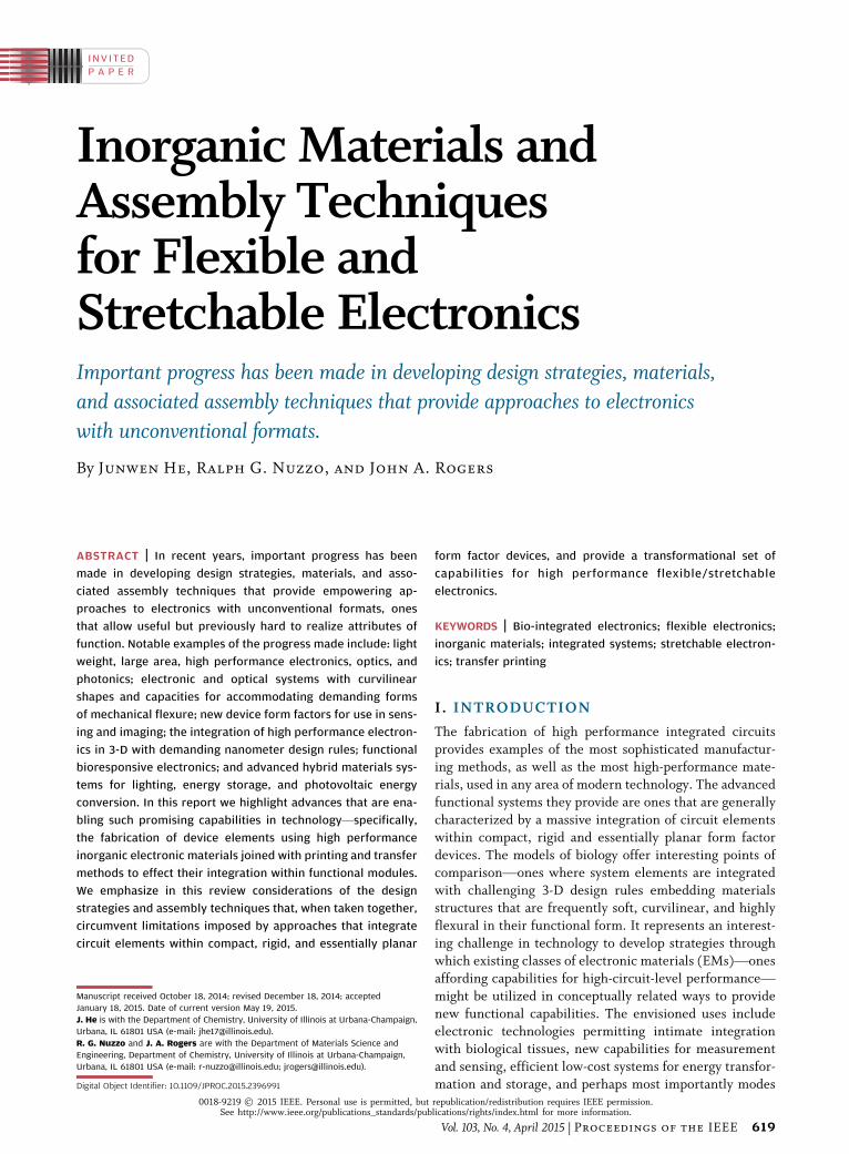
Fig. 1(a) illustrates one example, here aligned Ge/Si core/shell nanowire arrays which are used as the channel material
for field effect transistors (FETs) supported on a flexible
polyimide (PI) substrate. These arrays showed a modest
decrease in conductance (�6%) when bent to a radius of
2.5 mm along the axial direction [28]. In a similar fashion,
single-walled carbon nanotubes supported on polyethylene
terephthalate (PET) maintain high conductance even at a
bending radius of 1 mm owing to their small diameter
(1–2 nm) [29]. In some cases, tensile strains can be accom-
modated when the nanowires are deposited on a deformable
substrate in randomly oriented, multilayer forms. For exam-
ple, mesh-like 500 �m long Ag nanowire networks showedhigh conductance with excellent mechanical compliance to
strains reaching to 460% (defined by the substrate) [30].
Bundles of SWNTs ðlengths > 1 mmÞ also provide printable
routes to stretchable conductors, as illustrated in recent re-
port that dispersed the nanomaterial conductors in a rubber
matrix to form a gel-like conductive ink [31].
Fig. 1. Material configurations and structural layouts for flexible/stretchable electronics. (a) Aligned arrays of 1-D Ge/Si core/shell nanowire
arrays, here used as the channel materials for active-matrix FETs supported on a polyimide substrate. Reproduced with permission from [28].
Copyright American Chemical Society. (b) Patterned 2-D silicon nanoribbons undercut and delaminated from a Silicon-on-Insulator (SOI) wafer
using an isotropic wet-chemical etch of the buried oxide layer. Reproduced with permission from [35]. Copyright The American Association for the
Advancement of Science. (c) Ag nanoparticles patterned by direct-ink writing on a paper substrate. Reproduced with permission from [41].
Copyright John Wiley and Sons. (d) Buckled layout of printed silicon ribbons upon release of prestrain in the elastomeric (PDMS) substrate.
Reproduced with permission from [35]. Copyright The American Association for the Advancement of Science. (e) Planar Au filamentary serpentine
interconnects on an elastomeric substrate before (upper panel) and after (lower panel) compression. Reproduced with permission from [48].
Copyright IEEE. (f) Out-of-plane bridge interconnects for semiconductor circuits illustrating 3-D structural motifs formed by strain-minimizing
release dynamics Reproduced with permission from [51]. Copyright National Academy of Sciences, USA. (g) High performance GaAs solar
microcells interconnected by filamentary gold wires patterned in an open mesh layout to accommodate large amplitude strain evolution
in the supporting substrate. Reproduced with permission from [53]. Copyright John Wiley and Sons.
He et al. : Inorganic Materials and Assembly Techniques for Flexible and Stretchable Electronics
Vol. 103, No. 4, April 2015 | Proceedings of the IEEE 621
Similar forms of flexure can be realized using 2-D EMs,again with the proviso that they are thin. Systems of this
form, as exemplified by semiconductor nanomembranes
(NMs) and nanoribbons, have been intensively studied and
important advances towards mechanically robust systems
reported. For example, a fully functional cardio electro-
physiology sensor system integrating 2016 silicon NM
transistors on a plastic sheet allowed flexure to radii of
curvature as small as 500 �m without loss of performance[32]. A notable benefit attending the use of NM materials is
that they can be taken directly from high-purity single-
crystal wafers with proper release mechanisms and inte-
grated NM devices fabricated using well established means
of wafer scale processing [33]. For example, with suitable
alignment of trench cuts, silicon NM platelets and ribbons
can be released from a (111) silicon wafer by an anisotropic
wet etch with KOH; this is a procedure exploiting highlyanisotropic etching characteristics of low index Si planes
[34]. The image in Fig. 1(b) shows a related anisotropic wet-
etching fabrication method, here the buried oxide layer of a
silicon-on-insulator (SOI) wafer etched using HF to detach
silicon ribbons defined by a prior RIE trench cut [35]. An
intriguing example reported in the recent literature used
epitaxially grown multilayer stacks of GaAs thin film pho-
tovoltaic cells interspaced by layers of AlAs. The selectiveetching of the AlAs by HF allowed a quantitative release of
the high-efficiency GaAs PV microcells and recovery of the
growth substrate [36]. This latter example illustrates the
utility of NM materials for use in cases where high perfor-
mance electronics are required to meet application needs.
Specific examples of the latter are given in the sections
that follow.
Nanoparticles also comprise a system of great interestfor use as functional materials in flexible and stretchable
electronic devices. Metal nanoparticles in fluid suspen-
sion, for example, constitute a useful ink for printing metal
electrodes and bus-level interconnects [37], which, after
further processing by annealing [38] or laser sintering [39]
yield highly-conductive, and with proper design, flexible
metallic structures. An example of note was reported for a
silver nanoparticle ink [40] that was used to print Agstructures on a number of challenging substrates, includ-
ing paper and polyimide. The image in Fig. 1(c) shows a
section of a large area array of Ag conductors printed on
paper, structures which retained high conductivity to a
bending radius of 9 mm [41].
B. Form Factors for Extreme Flexureand Stretchability
There has now been substantial progress made in de-
vising form factors for electronics using inorganic EMs in
nanoscale form that can accommodate extremes in me-
chanics, including previously unprecedented capabilities
for flexure and stretching. The most effective design ap-
proach for electronics that can accommodate large ampli-
tude effective strains without fracture are based on various
forms of curvilinear/3-D integration of the electronic de-vice elements. Wavy structures of single-crystalline Si, for
example, can be fabricated by printing thin film ribbons on
a stretched elastomeric substrates. The release of the
prestrain leads to a buckling instability that forces the film
into a wavy configuration [42], [43], as illustrated by image
shown in Fig. 1(d). This allows an evolution of the strain in
the thin film during elongation (relaxation) that is much
smaller in magnitude than that experienced by the sub-strate [44]. It was found, for example, that 100 nm thick
single crystal silicon ribbons bonded on PDMS, similar to
the ones in Fig. 1(d), experience a peak strain during ten-
sile deformation that is 15 times less than that of the un-
derlying PDMS substrate [45].
A conceptually related example is based on a 2-D cur-
vilinear form. For this case, filamentary wires are pat-
terned as reiterative circular arcs that allow large tensiledeformations with minimum stress concentration [46].
The strain mitigation for structures of this type results due
to both elongation and some degree of out-of-plane deflec-
tion [47]. The Au wires shown in the Fig. 1(e) illustrates
the motif as applied to an array of serpentine interconnects
[48]. These specific structures were found to be mechan-
ically robustVwithstanding large magnitude bending,
stretching, compressive, and twisting deformations with-out fracturing. Computational models allow assessments of
the width and thickness, radius of curvature, and spacing
of the metal lines to optimize electrical and mechanical
performances [49]. Complex, open mesh configurations,
such as fractal designs [50], have also been proposed as a
means to accommodate more extreme forms of elastic de-
formation. Perhaps the most interesting strategies for ena-
bling extreme forms of mechanics are ones based onintrinsically 3-D forms of integration of the elementary
inorganic EM structures. This is illustrated by the example
shown in Fig. 1(f), where an interconnected square-mesh
of thin-film Si wires was bonded only at the nodes to a
prestrained elastomeric substrate. Release of the strain
leads to a popped-up motif of the interconnecting wires
which in turn serves a deformable bridge architecture [51].
The resulting interconnecting ‘‘bridges’’ can freely moveout of plane as shown in Fig. 1(f) and in this way provide a
robust means through which to accommodate 3-D forms of
large amplitude mechanical deformation.
The latter in-plane or out-of-plane designs appear to
be especially important as they allow the fabrication of
complex electronic systems as arrays in which highly
deformable/stretchable conductors can be used to inter-
connect active circuit components at nodes that experi-ence low strain. An exemplary case is illustrated by the
structures formed by 300 nm thick CMOS ribbons bridged
by polymer-embedded metal interconnection lines. When
printed on a prestrained PDMS surface [52], the wires
buckle vertically off the PDMS after release of the strainVforming a highly elastic noncoplanar mesh of bus inter-
connects. This structure can be compressed, stretched,
He et al. : Inorganic Materials and Assembly Techniques for Flexible and Stretchable Electronics
622 Proceedings of the IEEE | Vol. 103, No. 4, April 2015
twisted and sheared at a degree depending on the stiffnessand length of the bridges. Another intriguing example is
illustrated in Fig. 1(g), which shows 3.6 �m thick GaAs
solar microcells printed on textured PDMS islands with
each pixel separated by trenches and bridged by filamen-
tary gold interconnects. The maximum shear stress for this
layout is eight times less than that for a flat substrate [53].
Finally, we note that the failure of a circuit via a
mechanics-induced fracture can be mitigated by isolatingcomponents from the strain by adopting a neutral-
mechanical-plane design. To do so, a device element is
placed within a thin film at a location where strain is min-
imal for an arbitrary bending radius [52]. This is most
commonly done by coating the assembly with an additional
(e.g., polymeric) encapsulation layer [54]. This is a multi-
functional aspect of integration in that it can serve as a
means of both mechanical and environmental protection.
III . FABRICATION: PRINTING ANDTRANSFER ASSEMBLY METHODS
Any commercially viable flexible/stretchable electronics
will require reliable, high-throughput means of manufac-
turing. Owing to the small dimensions and mechanical
fragility of nanoscale inorganic EMs, their assembly andfunctional integration with high spatial and orientational
precision remains an important challenge towards which
considerable effort has been directed in research. Methods
exploiting self-assembly, in which EM structures and/or
device level components are placed in fluid suspensions
and deposited on a substrate by electrical/magnetic forces
[55], [56], flow fields, [57], [58], or recognition by surface
relief structures [37], have been intensively studied. Al-though they show promise, current capabilities remain less
than those required for commercial applications. Printing
techniques, of which many forms have been investigated,
constitute important and highly promising alternatives. We
highlight three exemplary cases that illustrate the potential
for printing (and the highly related technique of transfer
assembly) as approaches to manufacturing for flexible/
stretchable electronics.
A. Printing and Transfer AssemblyWet printing techniques, such as screen printing [59],
flexographic printing [60], and inkjet printing [61], to
name a few, have proven to be extremely useful in the
fabrication and assembly of organic electronics with appli-
cations ranging from organic LEDs [62], [63] to organic
solar cells [12], [64]. These methods, though, are mostlyrestricted to fluid inks of predefined requirements for vis-
cosity and homogeneity that limit their use with inorganic
EMs. One notable exception is found in printing nanopar-
ticle inks in a highly deterministic manner. For example,
direct ink writing represents an attractive approach, one
offering capabilities for patterning challenging geometries
embedding both 2-D and 3-D design rules [65], [66]. It is
an additive method of fabrication and in this regard offersuseful attributes that might complement more conven-
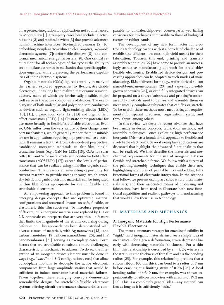
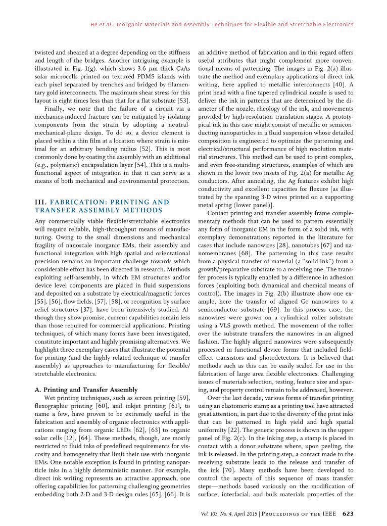
tional means of patterning. The images in Fig. 2(a) illus-
trate the method and exemplary applications of direct ink
writing, here applied to metallic interconnects [40]. A
print head with a fine tapered cylindrical nozzle is used to
deliver the ink in patterns that are determined by the di-
ameter of the nozzle, rheology of the ink, and movements
provided by high-resolution translation stages. A prototy-pical ink in this case might consist of metallic or semicon-
ducting nanoparticles in a fluid suspension whose detailed
composition is engineered to optimize the patterning and
electrical/structural performance of high resolution mate-
rial structures. This method can be used to print complex,
and even free-standing structures, examples of which are
shown in the lower two insets of Fig. 2(a) for metallic Ag
conductors. After annealing, the Ag features exhibit highconductivity and excellent capacities for flexure [as illus-
trated by the spanning 3-D wires printed on a supporting
metal spring (lower panel)].
Contact printing and transfer assembly frame comple-
mentary methods that can be used to pattern essentially
any form of inorganic EM in the form of a solid ink, with
exemplary demonstrations reported in the literature for
cases that include nanowires [28], nanotubes [67] and na-nomembranes [68]. The patterning in this case results
from a physical transfer of material (a ‘‘solid ink’’) from a
growth/preparative substrate to a receiving one. The trans-
fer process is typically enabled by a difference in adhesion
forces (exploiting both dynamical and chemical means of
control). The images in Fig. 2(b) illustrate show one ex-
ample, here the transfer of aligned Ge nanowires to a
semiconductor substrate [69]. In this process case, thenanowires were grown on a cylindrical roller substrate
using a VLS growth method. The movement of the roller
over the substrate transfers the nanowires in an aligned
fashion. The highly aligned nanowires were subsequently
processed in functional device forms that included field-
effect transistors and photodetectors. It is believed that
methods such as this can be easily scaled for use in the
fabrication of large area flexible electronics. Challengingissues of materials selection, testing, feature size and spac-
ing, and property control remain to be addressed, however.
Over the last decade, various forms of transfer printing
using an elastomeric stamp as a printing tool have attracted
great attention, in part due to the diversity of the print inks
that can be patterned in high yield and high spatial
uniformity [22]. The generic process is shown in the upper
panel of Fig. 2(c). In the inking step, a stamp is placed incontact with a donor substrate where, upon peeling, the
ink is released. In the printing step, a contact made to the
receiving substrate leads to the release and transfer of
the ink [70]. Many methods have been developed to
control the aspects of this sequence of mass transfer
stepsVmethods based variously on the modification of
surface, interfacial, and bulk materials properties of the
He et al. : Inorganic Materials and Assembly Techniques for Flexible and Stretchable Electronics
Vol. 103, No. 4, April 2015 | Proceedings of the IEEE 623
stamp/substrate pairings as well as the dynamics of the
adhesive forces. For the former, useful means include laser-
induced thermo-expansion [71], adhesion modification
layers [72], plasma activation [73], [74], and shape engineer-
ing of the stamp contact interface [75], [76]. For the latter
case, detailed mechanics models of the transfer processes[77] illustrate the essential role played by dynamics such as
shear [78] and/or peeling speed [79] in controlling the
attributes of mass transfer. The span of the design rules that
can be accommodated are vastVliterally spanning from
nanometers to many centimeters [80] depending on the
attributes of the stamps employed. Aided by automated tool
sets [81], printing accuracies of better than 200 nm [82] with
a throughput of over one million pixel elements per hour[80], [83] have been demonstrated, along with capabilities
for precise control over areal densities and stacking
configurations [84]. The image in the lower panel of
Fig. 2(c) presents an example illustrating such operative
capabilities, a section of a large area array of GaAs platelets
printed on a curvilinear substrate. A particular advantage of
the transfer-assembly method demonstrated here is that it is
a highly parallel method of printing that also remarkably
broadens the materials choices for inks by separating all
aspects of materials growth and preprint fabrication/processing from the inking and printing steps. It also
preserves the electronic properties of such generally fragile
nanomembrane/thin-film inks due to the soft nature of the
stamps and the generally non-destructive forces that mediate
the mass transfer. Given these potential advantages, transfer
printing stands almost alone in its capacity to enable the
high-throughput assembly of sophisticated/fully-functional
circuit-level componentsVan essential requirement forintegrating advanced functionalities (such as logic operation)
into flexible/stretchable electronics. In Section III-B, we
highlight several examples of functional, full device-level
inks of this type.
Fig. 2. Printing techniques with important applications in stretchable/flexible electronics. (a) A schematic depiction of direct ink writing
(upper panel); an exemplary silver interconnect in the form of self-supported arch printed over an intersecting bus line (middle panel);
self-supporting Ag wires printed on a compressed spring (lower panel), the inset shows the wires after extension on the spring. Reproduced
with permission from [40]. Copyright The American Association for the Advancement of Science. (b) Schematic depiction of a roller-based
contact printing apparatus for nanowire arrays (upper panel) and roll-to-roll printing of nanowires grown by a VLS process on the roller
printing head (middle panel); Aligned Ge nanowire arrays printed on a 4 in Si/SiO2 wafer (lower panel). Reproduced with permission from [69].
Copyright John Wiley and Sons. (c) Schematic depiction of transfer printing of a solid ink using an elastomeric stamp as a printing tool
showing the inking and transfer stages of the process (upper and middle panels); exemplary large area arrays of single-crystalline
GaAs micro-chiplet inks printed on a curvilinear surface (lower panel). Reproduced with permission from [70]. Copyright Nature
Publishing Group.
He et al. : Inorganic Materials and Assembly Techniques for Flexible and Stretchable Electronics
624 Proceedings of the IEEE | Vol. 103, No. 4, April 2015
B. Functional Electronic Inks for Flexible andStretchable Electronics
Inks arguably constitute the most important enabling
component of flexible/stretchable electronics enabled by
transfer assembly means of fabrication. They define such
features as the circuit-level functionality of the device, its
electronic performance attributes, and capabilities for ena-
bled applications. A large range of materials have been
prepared in forms that render them suitable for use asprintable inks for use in flexible and stretchable electronics
and other devices, including many examples of inorganic
semiconductors (e.g., as nanomembranes, nanoribbons,
nanowires, quantum dots [85], [86]), metallic nanoparti-
cles [87], [88], organic materials (e.g., polymeric resists
[89], [90] and even living cells [91], [92]). Low dimen-
sional, essentially 1-D materials, such as nanowires and
nanotubes, are particularly attractive materials for use ascomponents in high performance devices because of their
bendable structure and high electron mobility. Indeed, the
advantages afforded by these enabling attributes have been
demonstrated in a number of examples reported in the
recent literature. Notable examples include flexible opto-
electronic [93] and mechanical sensing devices [94] fab-
ricated using such active material elements. Even so, the
fabrication of complex flexible electronic systems usingsemiconductor nanowire arrays as a start remains limited
by numerous challenges that have yet to be fully addressed
in research. Of these, the typically poor thermal and che-
mical compatibilities of flexible substrate materials with
the harsh conditions required for post-print processing and
patterning of fully integrated electronic components are
particularly limiting. In addition, high degrees of precision
in layout and multilevel registration are difficult to obtainon substrates other than hard, planar handling/source
material wafers, which, because of error propagation,
limits the permitted levels of integration and thus
performance of the resulting circuit.
Fabrication methods based on transfer assembly, when
conjoined with 2-D EM inks derived from high-purity
single-crystalline wafers, can circumvent many of the
aforementioned limitations, not only because of their su-perior electronic properties but also due to their planar
geometryVone that is most compatible with both the es-
tablished tools and processes of microelectronics fabrica-
tion. The inks in this case are fully fabricated as a functional
2-D circuit element with all the required processing steps
carried out on an electronic grade semiconductor source
wafer using established procedures. The completed devices
are then released from the source wafer and printed on areceiving substrate using a scalable/highly-parallel
transfer-assembly method. The section that follows dis-
cusses several exemplary cases in which sophisticated/
highly-functional electronic inks are fabricated and
printed in this wayVbenchmarks establishing the enabling
promise of such materials for use in flexible/stretchable
electronics.
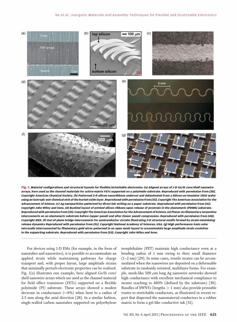
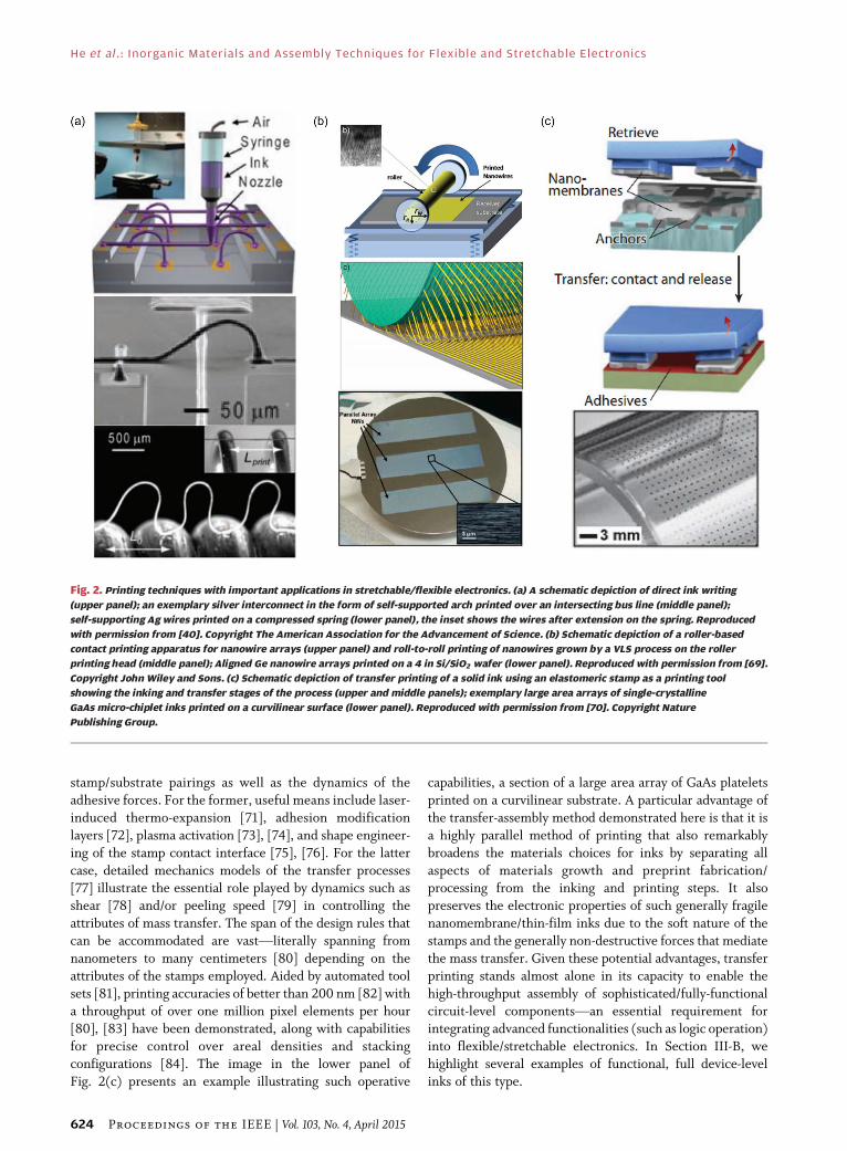
The image in the upper panel of Fig. 3(a) shows small,micron-scale InGaN LEDs after completion of their fabri-
cation and preparation for release from their material-
source wafer [95]. The MBE-grown multilayer stack
supported on a Si(111) base substrate was processed to
hold the undercut LEDs in place via a system of anchors
that are sacrificed during the printing step. Standard
techniques employed to fabricate the LED inks include
photolithographic patterning, epitaxial growth, reactive ionetching, contact metallurgy, thermal annealing, and aniso-
tropic wet chemical etching (of a sacrificial layer to effect
the undercutting). The resulting micro-LED arrays de-
veloped on the wafer in this way are fully functional, with
n- and p-type contact pads ready for interconnection. De-
terministic printing via a soft elastomeric stamp yields a
nondestructive and highly parallel transfer. This is illus-
trated by the image shown in the middle panel of Fig. 3(a),where the emission of a blue-emitting array of LEDs
printed on a polyimide substrate is shown after electrical
interconnection. The resulting LED devices show virtually
the same emission spectra and current-voltage character-
istics before and after the printing step, as is illustrated by
the data shown in the lower panel of Fig. 3(a).
As a second example, the upper panel of Fig. 3(b) shows
an array of silicon solar micro-cells embedded in a lumi-nescent solar concentrator waveguide by transfer printing
[96]. The individual cells in this case are 15 �m thick,
50 �m wide and several millimeters long. The cells are
processed prior to printing to enable high photon conver-
sion efficiencies to electrical power. A crucial sequence of
doping steps is needed to this end that carries a very high
thermal budget, a feature enabled by the fact that all the
microcell processing steps are carried out on the Si sourcewafer prior to printing. One notes that even with the high
aspect ratio of the embedded silicon micro-cells shown,
the printing is able to maintain the orientation and spacing
with high precision, thus allowing optimization of the
array to maximize light collection and conversion to elec-
trical energy. Encapsulation of the solar micro-cell arrays
yields a neutral mechanical plane design that shows both
mechanical and electronic robustness to bending radiireaching to 4.5 mm [lower panel of Fig. 3(b)].
As noted above, inks requiring extreme physicochem-
ical conditions during processing (e.g., metallization, dop-
ing, contact annealing, thermal oxidation, etc.) can be
developed on their material-source wafers, printed on a
common substrate, and after interconnection provide
system-level functionalities that can greatly enhance the
performance attributes of flexible/stretchable electronics.One notable example is shown in Fig. 3(c), where the
circuit-level integration of high performance silicon
MOSFET devices on a PI substrate are illustrated [97].
The individual silicon MOSFET devices were fabricated on
a SOI wafer using process steps that included solid-state
doping (1000 �C), thermal oxidation (1100 �C), RIE, wet
chemical etching, and PECVD processing. The devices are
He et al. : Inorganic Materials and Assembly Techniques for Flexible and Stretchable Electronics
Vol. 103, No. 4, April 2015 | Proceedings of the IEEE 625
shown supported by their anchors on the source wafer after
undercutting in the upper panel of Fig. 3(c). The deviceswere then printed onto a PI substrate, followed by metal
interconnection (middle panel). Electrical data measured
on the flexible substrate show sharp on-off transitions,
high field effect mobilities of 710 cm2v�1s�1, and sub-
threshold swings of 0.18 V decade�1, all indicating high
performance levels for the MOSFETs. Functional integ-
rated circuits, such as inverters, nor and nand logic gates,
were demonstrated as a proof of concept of the computingcapability for flexible electronics of this form.
IV. INTEGRATED SYSTEMS
Integrated flexible/stretchable electronic systems promise
system-level characteristics beyond what conventional on-
wafer layouts can provide. For example, a traditional emis-
sive display exploits fixed pixel arrays supported on a rigidglass panel. Printing methods provide interesting alter-
natives to the integration strategies used in such displays,
with attendant consequences for both weight and mechan-
ical durability [41]. Illuminating elements can be affixed
and connected in a desired manner on a flexible substrate
using only printing methods. An example of such is seen in
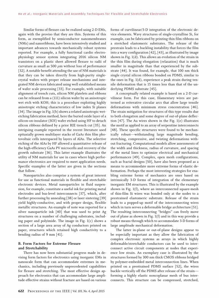
Fig. 4(a), where an interesting lighting effect of a single
LED chip mounted on paper is created using a hand-writtenconductive graphical trace. Fig. 4(b) shows a much larger
array of LEDs chips supported and similarly interconnected
on paper; the resulting module sustains high degrees of
curvilinear deformation without engendering critical fail-
ures of the electrical components. Another intriguing ex-
ample is shown in Fig. 4(c), an image showing a so-called
Fig. 3. (a) Micro-sized, blue emitting InGaN LEDs fabricated and supported on a mother wafer in a form suitable for use as a solid ink for functional
patterning using contact printing/transfer assembly methods (upper panel); An array of blue-emitting micro-LEDs printed and interconnected on
a supporting flexible substrate (middle panel), the small LEDs in this example contain an amount of semiconductor material that is approximately
the same as is found in one standard commercial LED; Current density-voltage curves and emission spectra before and after transfer printing,
showing only negligible performance differences (lower panel). Reproduced with permission from [95]. Copyright National Academy of Sciences,
USA. (b) Silicon solar microcells embedded as an array in a flexible luminescent solar concentrator (upper and middle panels). Data for the
photocurrents measured in different bending states showing that the electrical performance is not adversely impacted by mechanical flexure,
here ratio of short circuit currents ðI/I0Þ scaling in a manner that is proportional to ratio of projection area ða/a0Þ under normal incident
illumination (lower panel). Reproduced with permission from [96]. Copyright Nature Publishing Group. (c) Silicon-silicon dioxide MOSFETs
supported on wafer after fabrication prior to printing (upper panel); The same transistors after printing on a flexible polyimide (PI) substrate
(middle panel); Threshold voltage and mobility values for the MOSFETs plotted as a function of the channel length as measured on the PI substrate
(lower panel). Reproduced with permission from [97]. Copyright John Wiley and Sons.
He et al. : Inorganic Materials and Assembly Techniques for Flexible and Stretchable Electronics
626 Proceedings of the IEEE | Vol. 103, No. 4, April 2015
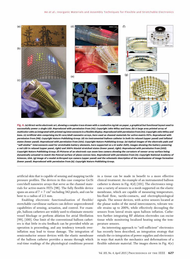
artificial skin that is capable of sensing and mapping tactile
pressure profiles. The devices in this case comprise Ge/Si
core/shell nanowire arrays that serve as the channel mate-
rials for active-matrix FETs [98]. The fully flexible device
spans an area of 7� 7 cm2 including 342 pixels, and can be
bent to a radius of 2.5 mm.
Enabling electronic functionalization of flexible/stretchable curvilinear surfaces can deliver unprecedented
capabilities of sensing, actuation, and control. For exam-
ple, balloon catheters are widely used to eliminate stenotic
vessel blockage or perform ablation for atrial fibrillation
[99], [100]. One limit of the conventional balloon cathet-
ers is that little in-situ feedback can be provided while an
operation is proceeding, and any tendency towards over-
inflation may lead to tissue damage. The integration ofsemiconductor sensor devices with the elastic membrane
of the balloon catheter provides a means through which
real-time readings of the physiological conditions present
in a tissue can be made in benefit to a more effective
clinical treatment. An example of an instrumented balloon
catheter is shown in Fig. 4(d) [101]. The electronics integ-
rate a variety of sensors in a mesh supported on the elastic
membrane, which are capable of measuring temperature,
bio-fluid flow, tactile-contacts, and electrophysiological
signals. The sensor devices, with active sensors located atthe planar nodes of the metal interconnects, tolerate ten-
sile strains up to 200%, while effectively decoupling the
sensors from lateral strain upon balloon inflation. Cathe-
ters further integrating RF ablation electrodes can excise
tissue while monitoring localized heating using the tem-
perature sensors.
An interesting approach to ‘‘self-sufficient’’ electronics
has recently been described, an integration strategy thatentails the co-integration of power supplies and electronics
in ways that match the mechanics and deformations of a
flexible substrate material. The images shown in Fig. 4(e)
Fig. 4. (a) Direct-write electronic art, showing a complex trace drawn with a conductive Ag ink on paper, a graphical but functional layout used to
successfully power a single LED. Reproduced with permission from [41]. Copyright John Wiley and Sons. (b) A large area printed array of
multicolor LEDs as integrated with printed Ag interconnects in a flexible display. Reproduced with permission from [41]. Copyright John Wiley and
Sons. (c) Artificial skin comprising Ge/Si core/shell nanowire arrays, here used as channel materials for active-matrix FETs. Reproduced with
permission from [98]. Copyright Nature Publishing Group. (d) An instrumented balloon catheter in both its relaxed (upper panel) and inflated
states (lower panel). Reproduced with permission from [101]. Copyright Nature Publishing Group. (e) Optical images of the electrode pads and
‘‘self-similar’’ interconnects used for stretchable battery elements, here supported on a Si wafer (left), images showing the battery powering
a red LED in relaxed (upper panel, right) and 300% biaxial stretched states (lower panel, right). Reproduced with permission from [102].
Copyright Nature Publishing Group. (f) Pictures of an electronic eye zoom lens camera showing the curvature of sensor array surface being
dynamically actuated to match the Petzval surface of plano-convex lens. Reproduced with permission from [4]. Copyright National Academy of
Sciences, USA. (g) Image of a model Arthropod eye camera (upper panel) and the schematic description of the mechanisms of image formation
(lower panel). Reproduced with permission from [6]. Copyright Nature Publishing Group.
He et al. : Inorganic Materials and Assembly Techniques for Flexible and Stretchable Electronics
Vol. 103, No. 4, April 2015 | Proceedings of the IEEE 627
illustrates an interesting example of a stretchable battery-powered device [102]. The layout of the design integrates
lithium battery disks (as well as electronics for wireless
recharging) that are interconnected by serpentine metal
wiresViterating ‘‘self-similar’’ arcs in a mesh network that
can undergo large magnitude stretching, folding, and twist-
ing deformations while maintaining high output voltage
and capacity, with a record tensile strain up to 300%. This
exceptionally compliant power system appears to be espe-cially well suited for use in lightweight and wearable
robotics.
An especially exciting application space for flexible/
stretchable electronics lies in the area of imaging. Support
for this contention can be developed by a consideration of
the modes of application of planar imaging media in camera
technology, in which optical aberration is usually overcome
by adding complexity to the lens system [103], dramaticallyincreasing the weight, bulk and (potentially) cost of the
device. For example, a simple lens renders a curved image
surface (Petzval surface) that is poorly matched to a planar
sensor array, requiring a compound lens system capable of
correcting off-axis rays [104]. A curved sensor array that
can adapt to the Petzval surface provides an alternative
design rule for an aberration-free imaging system [5]. The
system shown in Fig. 4(f) illustrates one approach to such adesign [4]. The camera (upper panel) integrates a fluidi-
cally actuated plano-convex lens whose curvature can be
continuously adjusted by the fluid pressure. An array of
silicon photo-detectors, transfer-printed and intercon-
nected on a stretchable membrane whose curvature can
be similarly varied is mounted beneath it (lower panels of
Fig. 4(f)). The assembly forms an adjustable zoom lens that
can render an image precisely on the surface of a matchingsensor array. The design shown here can be generalized to a
model for a camera that embeds a compound lens system
reminiscent of those of arthropod eyes [6]. In this case,
transfer-printed silicon photodiode arrays supported on an
elastic membrane are aligned and bonded to a deformable
PDMS micro-lens array. Actuation yields a hemispherical
deformation mimicking the compound apposition layouts
of arthropod eyes, as illustrated in Fig. 4(g). Precise engi-neering of the curvature of the system and the config-
uration of the individual micro-lenses provides a nearly
infinite depth of field, together with a wide field of view of
about 160- without off axis aberration. Possible applica-
tions include ones in intelligence/surveillance and endos-
copy. Taken together, these novel designs suggest the
potential for important impacts that might be realized
based on adoption of advanced materials and manufactur-ing concepts of flexible/stretchable electronics.
V. BIO-INTEGRATED ELECTRONICS
We finally close with a consideration of the potential im-
pacts that might come from the capability of assembling
electronic devices in flexible/stretchable configurations
that can innately support their integration with living sys-tems. This represents one of the most challenging scenarios
in which any electronic device of this form might be
employed. By necessity, they must be compliant enough to
laminate on or affix to soft/curvilinear tissues without eli-
citing deleterious mechanical stresses, yet be sufficiently
robust to sustain adhesion, resist moisture and chemical
degradation, and withstand fatigue due to tissue motion.
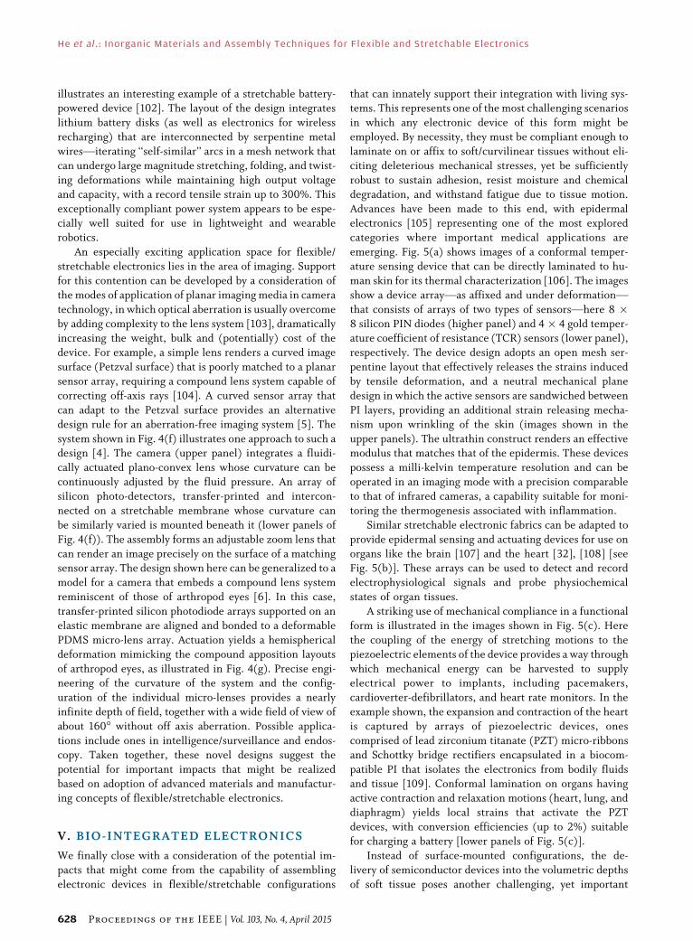
Advances have been made to this end, with epidermalelectronics [105] representing one of the most explored
categories where important medical applications are
emerging. Fig. 5(a) shows images of a conformal temper-
ature sensing device that can be directly laminated to hu-
man skin for its thermal characterization [106]. The images
show a device arrayVas affixed and under deformationVthat consists of arrays of two types of sensorsVhere 8 �8 silicon PIN diodes (higher panel) and 4� 4 gold temper-ature coefficient of resistance (TCR) sensors (lower panel),
respectively. The device design adopts an open mesh ser-
pentine layout that effectively releases the strains induced
by tensile deformation, and a neutral mechanical plane
design in which the active sensors are sandwiched between
PI layers, providing an additional strain releasing mecha-
nism upon wrinkling of the skin (images shown in the
upper panels). The ultrathin construct renders an effectivemodulus that matches that of the epidermis. These devices
possess a milli-kelvin temperature resolution and can be
operated in an imaging mode with a precision comparable
to that of infrared cameras, a capability suitable for moni-
toring the thermogenesis associated with inflammation.
Similar stretchable electronic fabrics can be adapted to
provide epidermal sensing and actuating devices for use on
organs like the brain [107] and the heart [32], [108] [seeFig. 5(b)]. These arrays can be used to detect and record
electrophysiological signals and probe physiochemical
states of organ tissues.
A striking use of mechanical compliance in a functional
form is illustrated in the images shown in Fig. 5(c). Here
the coupling of the energy of stretching motions to the
piezoelectric elements of the device provides a way through
which mechanical energy can be harvested to supplyelectrical power to implants, including pacemakers,
cardioverter-defibrillators, and heart rate monitors. In the
example shown, the expansion and contraction of the heart
is captured by arrays of piezoelectric devices, ones
comprised of lead zirconium titanate (PZT) micro-ribbons
and Schottky bridge rectifiers encapsulated in a biocom-
patible PI that isolates the electronics from bodily fluids
and tissue [109]. Conformal lamination on organs havingactive contraction and relaxation motions (heart, lung, and
diaphragm) yields local strains that activate the PZT
devices, with conversion efficiencies (up to 2%) suitable
for charging a battery [lower panels of Fig. 5(c)].
Instead of surface-mounted configurations, the de-
livery of semiconductor devices into the volumetric depths
of soft tissue poses another challenging, yet important
He et al. : Inorganic Materials and Assembly Techniques for Flexible and Stretchable Electronics
628 Proceedings of the IEEE | Vol. 103, No. 4, April 2015
opportunity for the use of flexible/stretchable electronics
in areas of medicine. Important distinctions can be made
between rigid device form factors, such as based on pene-
trating electrodes [110] or fibers [111], and a soft device
that can minimize tissue damage, inflammation, and scar-
ring. These ideas are illustrated in Fig. 5(d), which shows a
GaN LED, Si photo-detector, Pt thermo-resistor and a Pt
electrode of cellular scale fabricated on narrow, thin plas-tic strips by established micro-fabrication and transfer-
printing techniques (upper panel on left) [112]. They are
aligned and stacked in a layer-by-layer manner, resulting in
a flexible, multifunctional device of a total thickness of
�20 �m. Owing to its compliant nature, the ultrathin de-
vice is inserted into deep tissue using a releasable injection
needle in a minimally invasive operation, and once placed
can deliver photons to a targeted location with high spatial
and orientational precision. The data coming from these
studies, which reveal significant differences in biological
response as compared to fiber optic probes, suggest that
devices of this type will provide a powerful new tool for use
in the field of optogenetics.
VI. CONCLUSION
As discussed in this review, the emerging design strategies,
advanced materials in the form of high performance
Fig. 5. (a) Epidermal temperature sensor array laminated on human skin for thermal characterization (upper panel), with sensitivities
comparable to commercial infrared camera and capabilities for imaging-mode measurements (lower panel). Reproduced with permission
from [106]. Copyright Nature Publishing Group. (b) Integrated conformal sensor arrays laminated onto a living rabbit’s heart. The panel shown
at lower right is a spatial map of the electrical activation time measured on the posterior surfaces of the heart. Reproduced with permission
from [108]. Copyright Nature Publishing Group. (c) Optical image of piezoelectric PZT ribbons printed onto a PI thin film substrate (upper left)
and an integrated device mounted on a bovine heart (upper right), with data showing piezoelectric activation and voltage output coming
from piezoelectric energy transformation (lower left); the data given in the panel at the lower right shows battery voltage plotted against
time during charging by the PZT system. Reproduced with permission from [109]. Copyright National Academy of Sciences, USA. (d) Integrated
electrooptical micro-devices supported on a thin plastic strip; the devices shown have sizes much smaller than 200 �m fiber optic implant
more commonly used in optogenetics protocols (upper panel, left). A mouse after device implantation into deep-brain tissue for wireless
optogenetics experiments (lower left). The panel at higher right shows the injection of the device into deep structures of the brain. After
1 h of photostimulation, appreciable differences in expressed biomolecular species are found between an implanted fiber optic probe and the
flexible integrated device, results suggestive of different levels of trauma/functional response (lower panel, right). Reproduced with permission
from [112]. Copyright The American Association for the Advancement of Science.
He et al. : Inorganic Materials and Assembly Techniques for Flexible and Stretchable Electronics
Vol. 103, No. 4, April 2015 | Proceedings of the IEEE 629
inorganic EM inks, and enabling means of fabrication viaprinting and transfer assembly are providing a practical
foundation for the development of flexible/stretchable elec-
tronics with far ranging potential for engendering impacts in
technology. The devices so enabled provide useful, new, and
in many instances previously difficult to realize functional
capabilities for electronics while retaining levels of perfor-
mance more typically associated with chip-based, high-
integration electronics. It is now well appreciated that theprogress being made in research on unconventional form
factors for electronics will likely transform many areas of
technology, with perhaps the most profound impacts being
felt in areas of consumer electronicsVflexible light weight
displays, wearable electronics being notable examples. The
work highlighted above supports this assessment, but also
suggests an importance for technologies that will be quite
different in terms of the nature of the manufacturing regimethey would need for commercial success. In our view, the
development of an enabling electronics technology thatseamlessly merges the form factor of high performance
electronics with those of complex systems and phenomen-
aVthe soft, adaptive, and hierarchical forms of living
systems or the curvilinear designs that innately mesh with
optics, as examplesVstands as both a frontier challenge for
engineering research and significant opportunity for prog-
ress in technology. As the highlights given above suggest, the
progress made in a very short time is remarkable. Moreimportantly, though, the pace of advancement towards com-
mercialized objectives is clearly accelerating. All the same,
we have only begun to imagine what might be possible. h
Acknowledgment
This work was supported by the U.S. Department of
Energy, Office of Science, Basic Energy Sciences, underAward # DE-FG02-07ER46471.
REF ERENCE S
[1] I. L. Markov, ‘‘Limits on fundamentallimits to computation,’’ Nature, vol. 512,pp. 147–154, Aug. 2014.
[2] T. Sekitani and T. Someya, ‘‘Stretchableorganic integrated circuits for large-areaelectronic skin surfaces,’’ MRS Bulletin,vol. 37, pp. 236–245, 2012.
[3] J. A. Rogers, ‘‘Bio-integrated electronics,’’ inIEEE Int. Electron Devices Meet. (IEDM),2012, pp. 1.1.1–1.1.4.
[4] I. Jung et al., ‘‘Dynamically tunablehemispherical electronic eye camera systemwith adjustable zoom capability,’’ Proc.Nat. Academy Sci., vol. 108, pp. 1788–1793,Feb. 1, 2011.
[5] H. C. Ko et al., ‘‘A hemisphericalelectronic eye camera based on compressiblesilicon optoelectronics,’’ Nature, vol. 454,pp. 748–753, Aug. 2008.
[6] Y. M. Song et al., ‘‘Digital cameras withdesigns inspired by the arthropod eye,’’Nature, vol. 497, pp. 95–99, May 2013.
[7] J.-W. Jeong et al., ‘‘Materials and optimizeddesigns for human-machine interfaces viaepidermal electronics,’’ Adv. Mater., vol. 25,pp. 6839–6846, 2013.
[8] C. Yu et al., ‘‘Adaptive optoelectroniccamouflage systems with designs inspiredby cephalopod skins,’’ Proc. Nat. AcademySci., Aug. 18, 2014.
[9] R. D. Kornbluh et al., ‘‘Dielectricelastomers: Stretching the capabilitiesof energy harvesting,’’ MRS Bulletin,vol. 37, pp. 246–253, 2012.
[10] J. Burroughes et al., ‘‘Light-emitting diodesbased on conjugated polymers,’’ Nature,vol. 347, pp. 539–541, 1990.
[11] S. Reineke et al., ‘‘White organiclight-emitting diodes with fluorescenttube efficiency,’’ Nature, vol. 459,pp. 234–238, May 2009.
[12] S. Gunes, H. Neugebauer, and N. S. Sariciftci,‘‘Conjugated polymer-based organic solarcells,’’ Chem. Rev., vol. 107, pp. 1324–1338,2007.
[13] H. Hoppe and N. S. Sariciftci, ‘‘Organicsolar cells: An overview,’’ J. Mater. Res.,vol. 19, pp. 1924–1945, 2004.
[14] J. Zaumseil and H. Sirringhaus, ‘‘Electronand ambipolar transport in organic
field-effect transistors,’’ Chem. Rev.,vol. 107, pp. 1296–1323, 2007.
[15] T. Fujii et al., ‘‘Increase in the extractionefficiency of GaN-based light-emitting diodesvia surface roughening,’’ Appl. Phys. Lett.,vol. 84, pp. 855–857, 2004.
[16] G. J. Bauhuis, P. Mulder, E. J. Haverkamp,J. C. C. M. Huijben, and J. J. Schermer,‘‘26.1% thin-film GaAs solar cell usingepitaxial lift-off,’’ Solar Energy Mater. SolarCells, vol. 93, pp. 1488–1491, Sep. 2009.
[17] S. Y. Chou, D. A. Antoniadis, and H. I. Smith,‘‘Observation of electron velocity overshootin sub-100-nm-channel MOSFET’s insilicon,’’ IEEE Electron Device Lett., vol. 6,pp. 665–667, 1985.
[18] S. De et al., ‘‘Silver nanowire networks asflexible, transparent, conducting films:Extremely high DC to optical conductivityratios,’’ ACS Nano, vol. 3, pp. 1767–1774,Jul. 2009.
[19] Q. Cao et al., ‘‘Medium-scale carbonnanotube thin-film integrated circuitson flexible plastic substrates,’’ Nature,vol. 454, pp. 495–500, Jul. 2008.
[20] W. Shi et al., ‘‘Free-standing single crystalsilicon nanoribbons,’’ J. Amer. Chem. Soc.,vol. 123, pp. 11095–11096, 2001.
[21] Y. Weiquan et al., ‘‘Large-area InP-basedcrystalline nanomembrane flexiblephotodetectors,’’ Appl. Phys. Lett.,vol. 96, pp. 121107-1–121107-3, 2010.
[22] A. Carlson, A. M. Bowen, Y. G. Huang,R. G. Nuzzo, and J. A. Rogers, ‘‘Transferprinting techniques for materials assemblyand micro/nanodevice fabrication,’’ Adv.Mater., vol. 24, pp. 5284–5318, Oct. 2012.
[23] M. M. Roberts et al., ‘‘Elasticallyrelaxed free-standing strained-siliconnanomembranes,’’ Nat. Mater., vol. 5,pp. 388–393, May 2006.
[24] Y. Wu and P. Yang, ‘‘Direct observation ofvapor-liquid-solid nanowire growth,’’ J. Amer.Chem. Soc., vol. 123, pp. 3165–3166, 2001.
[25] Z. Suo, E. Y. Ma, H. Gleskova, andS. Wagner, ‘‘Mechanics of rollable andfoldable film-on-foil electronics,’’ Appl.Phys. Lett., vol. 74, pp. 1177–1179, 1999.
[26] A. J. Baca et al., ‘‘Semiconductor wiresand ribbons for high-performance flexibleelectronics,’’ Angewandte Chemie-Int. Ed.,vol. 47, pp. 5524–5542, 2008.
[27] G. Stan, S. Krylyuk, A. V. Davydov, I. Levin,and R. F. Cook, ‘‘Ultimate bending strengthof Si nanowires,’’ Nano Lett., vol. 12,pp. 2599–2604, May 2012.
[28] Z. Fan et al., ‘‘Wafer-scale assembly of highlyordered semiconductor nanowire arraysby contact printing,’’ Nano Lett., vol. 8,pp. 20–25, Jan. 2007.
[29] P. H. Lau et al., ‘‘Fully printed, highperformance carbon nanotube thin-filmtransistors on flexible substrates,’’ NanoLett., vol. 13, pp. 3864–3869, Aug. 2013.
[30] P. Lee et al., ‘‘Highly stretchable and highlyconductive metal electrode by very longmetal nanowire percolation network,’’Adv. Mater., vol. 24, pp. 3326–3332,2012.
[31] T. Sekitani et al., ‘‘Stretchable active-matrixorganic light-emitting diode display usingprintable elastic conductors,’’ Nat. Mater.,vol. 8, pp. 494–499, Jun. 2009.
[32] J. Viventi et al., ‘‘A conformal, bio-interfacedclass of silicon electronics for mappingcardiac electrophysiology,’’ Sci. TranslationalMed., vol. 2, p. 24ra22, Mar. 2010.
[33] J. A. Rogers, M. G. Lagally, and R. G. Nuzzo,‘‘Synthesis, assembly and applications ofsemiconductor nanomembranes,’’ Nature,vol. 477, pp. 45–53, Sep. 2011.
[34] H. C. Ko, A. J. Baca, and J. A. Rogers,‘‘Bulk quantities of single-crystal siliconmicro-/nanoribbons generated from bulkwafers,’’ Nano Lett., vol. 6, pp. 2318–2324,Oct. 2006.
[35] D.-Y. Khang, H. Jiang, Y. Huang, andJ. A. Rogers, ‘‘A stretchable form ofsingle-crystal silicon for high-performanceelectronics on rubber substrates,’’ Sci.,vol. 311, pp. 208–212, Jan. 13, 2006.
[36] J. Yoon et al., ‘‘GaAs photovoltaics andoptoelectronics using releasable multilayerepitaxial assemblies,’’ Nature, vol. 465,pp. 329–U80, May 2010.
[37] I. Park et al., ‘‘Nanoscale patterning andelectronics on flexible substrate by directnanoimprinting of metallic nanoparticles,’’Adv. Mater., vol. 20, pp. 489–496, 2008.
[38] A. Hu et al., ‘‘Low temperature sinteringof Ag nanoparticles for flexible electronicspackaging,’’ Appl. Phys. Lett., vol. 97,p. 153117, 2010.
He et al. : Inorganic Materials and Assembly Techniques for Flexible and Stretchable Electronics
630 Proceedings of the IEEE | Vol. 103, No. 4, April 2015
[39] S. H. Ko et al., ‘‘All-inkjet-printedflexible electronics fabrication on apolymer substrate by low-temperaturehigh-resolution selective laser sinteringof metal nanoparticles,’’ Nanotechnol.,vol. 18, p. 345202, 2007.
[40] B. Y. Ahn et al., ‘‘Omnidirectional printingof flexible, stretchable, and spanningsilver microelectrodes,’’ Sci., vol. 323,pp. 1590–1593, Mar. 20, 2009.
[41] A. Russo et al., ‘‘Pen-on-paper flexibleelectronics,’’ Adv. Mater., vol. 23,pp. 3426–3430, 2011.
[42] S. Wagner et al., ‘‘Electronic skin:Architecture and components,’’ Phys. E:Low-Dimensional Syst. Nanostructures,vol. 25, pp. 326–334, Nov. 2004.
[43] A. L. Volynskii, S. Bazhenov, O. V. Lebedeva,and N. F. Bakeev, ‘‘Mechanical bucklinginstability of thin coatings deposited on softpolymer substrates,’’ J. Mater. Sci., vol. 35,pp. 547–554, Feb. 2000.
[44] J. A. Rogers, T. Someya, and Y. Huang,‘‘Materials and mechanics for stretchableelectronics,’’ Sci., vol. 327, pp. 1603–1607,Mar. 26, 2010.
[45] H. Jiang et al., ‘‘Finite deformationmechanics in buckled thin films oncompliant supports,’’ Proc. Nat. Academy Sci.,vol. 104, pp. 15 607–15 612, Oct. 2, 2007.
[46] M. Gonzalez et al., ‘‘Design of metalinterconnects for stretchable electroniccircuits,’’ Microelectron. Reliab., vol. 48,pp. 825–832, Jun. 2008.
[47] S. P. Lacour, D. Chan, S. Wagner,T. Li, and Z. Suo, ‘‘Mechanisms of reversiblestretchability of thin metal films onelastomeric substrates,’’ Appl. Phys. Lett.,vol. 88, p. 204103, 2006.
[48] D. Brosteaux, F. Axisa, M. Gonzalez, andJ. Vanfleteren, ‘‘Design and fabricationof elastic interconnections for stretchableelectronic circuits,’’ IEEE Electron DeviceLett., vol. 28, pp. 552–554, 2007.
[49] W. Cao, P. Gorrn, and S. Wagner, ‘‘Modelingthe electrical resistance of gold filmconductors on uniaxially stretchedelastomeric substrates,’’ Appl. Phys.Lett., vol. 98, p. 212112, 2011.
[50] J. A. Fan et al., ‘‘Fractal design conceptsfor stretchable electronics,’’ Nat. Commun.,vol. 5, Feb. 2014.
[51] D.-H. Kim et al., ‘‘Materials and noncoplanarmesh designs for integrated circuitswith linear elastic responses to extrememechanical deformations,’’ Proc. Nat.Academy Sci., vol. 105, pp. 18 675–18 680,Dec. 2, 2008.
[52] D.-H. Kim et al., ‘‘Stretchable and foldablesilicon integrated circuits,’’ Sci., vol. 320,pp. 507–511, Apr. 25, 2008.
[53] J. Lee et al., ‘‘Stretchable GaAs photovoltaicswith designs that enable high arealcoverage,’’ Adv. Mater., vol. 23, pp. 986–991,2011.
[54] S.-I. Park et al., ‘‘Theoretical andexperimental studies of bending ofinorganic electronic materials on plasticsubstrates,’’ Adv. Functional Mater., vol. 18,pp. 2673–2684, 2008.
[55] P. A. Smith et al., ‘‘Electric-field assistedassembly and alignment of metallicnanowires,’’ Appl. Phys. Lett., vol. 77,pp. 1399–1401, 2000.
[56] Y. Cao et al., ‘‘A technique for controllingthe alignment of silver nanowires with anelectric field,’’ Nanotechnol., vol. 17, p. 2378,2006.
[57] Y. Huang, X. Duan, Q. Wei, and C. M. Lieber,‘‘Directed assembly of one-dimensionalnanostructures into functional networks,’’Sci., vol. 291, pp. 630–633, Jan. 26, 2001.
[58] K. Oh, J.-H. Chung, J. J. Riley,Y. Liu, and W. K. Liu, ‘‘Fluid flow-assisteddielectrophoretic assembly of nanowires,’’Langmuir, vol. 23, pp. 11 932–11 940,Nov. 2007.
[59] D. A. Pardo, G. E. Jabbour, andN. Peyghambarian, ‘‘Application ofscreen printing in the fabrication oforganic light-emitting devices,’’ Adv.Mater., vol. 12, pp. 1249–1252, 2000.
[60] F. C. Krebs, J. Fyenbo, and M. Jørgensen,‘‘Product integration of compact roll-to-rollprocessed polymer solar cell modules:Methods and manufacture using flexographicprinting, slot-die coating and rotaryscreen printing,’’ J. Mater. Chem., vol. 20,pp. 8994–9001, 2010.
[61] H. Sirringhaus et al., ‘‘High-resolution inkjetprinting of all-polymer transistor circuits,’’Sci., vol. 290, pp. 2123–2126, 2000.
[62] P. Kopola, M. Tuomikoski, R. Suhonen, andA. Maaninen, ‘‘Gravure printed organic lightemitting diodes for lighting applications,’’Thin Solid Films, vol. 517, pp. 5757–5762,2009.
[63] D.-Y. Chung, J. Huang, D. D. Bradley, andA. J. Campbell, ‘‘High performance, flexiblepolymer light-emitting diodes (PLEDs) withgravure contact printed hole injection andlight emitting layers,’’ Organic Electron.,vol. 11, pp. 1088–1095, 2010.
[64] F. C. Krebs, ‘‘Fabrication and processingof polymer solar cells: A review of printingand coating techniques,’’ Solar Energy Mater.Solar Cells, vol. 93, pp. 394–412, 2009.
[65] K. Sun et al., ‘‘3D printing of interdigitatedli-ion microbattery architectures,’’ Adv.Mater., vol. 25, pp. 4539–4543, 2013.
[66] B. Y. Ahn, D. J. Lorang, and J. A. Lewis,‘‘Transparent conductive grids via directwriting of silver nanoparticle inks,’’Nanoscale, vol. 3, pp. 2700–2702, 2011.
[67] C. L. Pint et al., ‘‘Dry contact transferprinting of aligned carbon nanotubepatterns and characterization oftheir optical properties for diameterdistribution and alignment,’’ ACS Nano,vol. 4, pp. 1131–1145, Feb. 2010.
[68] S. Bae et al., ‘‘Roll-to-roll production of30-inch graphene films for transparentelectrodes,’’ Nat. Nano., vol. 5, pp. 574–578,Aug. 2010.
[69] Z. Fan et al., ‘‘Toward the developmentof printable nanowire electronics andsensors,’’ Adv. Mater., vol. 21, pp. 3730–3743,2009.
[70] D.-H. Kim, N. Lu, R. Ghaffari, andJ. A. Rogers, ‘‘Inorganic semiconductornanomaterials for flexible and stretchablebio-integrated electronics,’’ NPG Asia Mater,vol. 4, p. e15, Apr. 2012.
[71] R. Saeidpourazar et al., ‘‘Laser-drivenmicro transfer placement of prefabricatedmicrostructures,’’ J. Microelectromechan.Syst., vol. 21, pp. 1049–1058, 2012.
[72] T.-H. Kim et al., ‘‘Full-colour quantumdot displays fabricated by transfer printing,’’Nat. Photon, vol. 5, pp. 176–182, Mar. 2011.
[73] Y.-L. Loo, R. L. Willett, K. W. Baldwin, andJ. A. Rogers, ‘‘Interfacial chemistries fornanoscale transfer printing,’’ J. Amer. Chem.Soc., vol. 124, pp. 7654–7655, Jul. 2002.
[74] B. A. Langowski and K. E. Uhrich, ‘‘Oxygenplasma-treatment effects on Si transfer,’’Langmuir, vol. 21, pp. 6366–6372, Jul. 2005.
[75] J. Wu et al., ‘‘Contact radius of stampsin reversible adhesion,’’ Theoretical Appl.Mechan. Lett., vol. 1, p. 011001, 2011.
[76] J. Wu et al., ‘‘Mechanics ofreversible adhesion,’’ Soft Matter,vol. 7, pp. 8657–8662, 2011.
[77] X. Feng et al., ‘‘Competing fracture inkinetically controlled transfer printing,’’Langmuir, vol. 23, pp. 12 555–12 560,Dec. 2007.
[78] A. Carlson et al., ‘‘Shear-enhancedadhesiveless transfer printing for use indeterministic materials assembly,’’ Appl.Phys. Lett., vol. 98, p. 264104, 2011.
[79] M. A. Meitl et al., ‘‘Transfer printing bykinetic control of adhesion to an elastomericstamp,’’ Nat. Mater., vol. 5, pp. 33–38,Jan. 2006.
[80] D. Chanda et al., ‘‘Large-area flexible 3Doptical negative index metamaterial formedby nanotransfer printing,’’ Nat. Nano., vol. 6,pp. 402–407, Jul. 2011.
[81] N. Ahmed, A. Carlson, J. A. Rogers, andP. M. Ferreira, ‘‘Automated micro-transferprinting with cantilevered stamps,’’ J.Manufacturing Processes, vol. 14, pp. 90–97,Apr. 2012.
[82] A. J. Trindade et al., ‘‘Nanoscale-accuracytransfer printing of ultra-thin AlInGaNlight-emitting diodes onto mechanicallyflexible substrates,’’ Appl. Phys. Lett.,vol. 103, p. 253302, 2013.
[83] C. A. Bower, E. Menard, and P. E. Garrou,‘‘Transfer printing: An approach formassively parallel assembly of microscaledevices,’’ in Proc. 58th Electron. ComponentsTechnol. Conf. (ECTC), 2008, pp. 1105–1109.
[84] S. Kim et al., ‘‘Microstructured elastomericsurfaces with reversible adhesion andexamples of their use in deterministicassembly by transfer printing,’’ Proc. Nat.Academy Sci., vol. 107, pp. 17 095–17 100,Oct. 5, 2010.
[85] A. Rizzo et al., ‘‘Hybrid light-emitting diodesfrom microcontact-printing double-transferof colloidal semiconductor CdSe/ZnSquantum dots onto organic layers,’’ Adv.Mater., vol. 20, pp. 1886–1891, 2008.
[86] L. Kim et al., ‘‘Contact printing of quantumdot light-emitting devices,’’ Nano Lett., vol. 8,pp. 4513–4517, Dec. 2008.
[87] M. Xue et al., ‘‘Transfer printing ofmetal nanoparticles with controllabledimensions, placement, and reproduciblesurface-enhanced raman scattering effects,’’Langmuir, vol. 25, pp. 4347–4351, Apr. 2009.
[88] N. A. Abu Hatab, J. M. Oran, andM. J. Sepaniak, ‘‘Surface-enhanced ramanspectroscopy substrates created via electronbeam lithography and nanotransferprinting,’’ ACS Nano, vol. 2, pp. 377–385,Feb. 2008.
[89] W. R. Childs and R. G. Nuzzo, ‘‘Patterningof thin-film microstructures on non-planarsubstrate surfaces using decal transferlithography,’’ Adv. Mater., vol. 16,pp. 1323–1327, 2004.
[90] W. R. Childs and R. G. Nuzzo, ‘‘Decaltransfer microlithography: A newsoft-lithographic patterningmethod,’’ J. Amer. Chem. Soc., vol. 124,pp. 13 583–13 596, Nov. 2002.
[91] H. Xu et al., ‘‘Microcontact printing ofdendrimers, proteins, and nanoparticlesby porous stamps,’’ J. Amer. Chem. Soc.,vol. 131, pp. 797–803, Jan. 2008.
[92] M. M. Stevens et al., ‘‘Direct patterningof mammalian cells onto poroustissue engineering substrates using
He et al. : Inorganic Materials and Assembly Techniques for Flexible and Stretchable Electronics
Vol. 103, No. 4, April 2015 | Proceedings of the IEEE 631
agarose stamps,’’ Biomaterials, vol. 26,pp. 7636–7641, Dec. 2005.
[93] Y. Li, F. Qian, J. Xiang, and C. M. Lieber,‘‘Nanowire electronic and optoelectronicdevices,’’ Materials Today, vol. 9, pp. 18–27,Oct. 2006.
[94] J. Zhou et al., ‘‘Flexible piezotronic strainsensor,’’ Nano Lett., vol. 8, pp. 3035–3040,Sep. 2008.
[95] H.-S. Kim et al., ‘‘Unusual strategies for usingindium gallium nitride grown on silicon(111) for solid-state lighting,’’ Proc. Nat.Academy Sci., vol. 108, pp. 10 072–10 077,Jun. 21, 2011.
[96] J. Yoon et al., ‘‘Flexible concentratorphotovoltaics based on microscale siliconsolar cells embedded in luminescentwaveguides,’’ Nature Commun., vol. 2,Jun. 2011.
[97] H.-J. Chung et al., ‘‘Fabrication of releasablesingle-crystal silicon-metal oxide field-effectdevices and their deterministic assemblyon foreign substrates,’’ Adv. FunctionalMater., vol. 21, pp. 3029–3036, 2011.
[98] K. Takei et al., ‘‘Nanowire active-matrixcircuitry for low-voltage macroscale artificialskin,’’ Nat. Mater., vol. 9, pp. 821–826,Oct. 2010.
[99] R. L. Mueller and T. A. Sanborn, ‘‘Thehistory of interventional cardiology: Cardiaccatheterization, angioplasty, and relatedinterventions,’’ Amer. Heart J., vol. 129,pp. 146–172, Jan. 1995.
[100] I. M. Robbins et al., ‘‘Pulmonary veinstenosis after catheter ablation ofatrial fibrillation,’’ Circulation, vol. 98,pp. 1769–1775, Oct. 27, 1998.
[101] D.-H. Kim et al., ‘‘Materials formultifunctional balloon catheters withcapabilities in cardiac electrophysiologicalmapping and ablation therapy,’’ Nat. Mater.,vol. 10, pp. 316–323, Apr. 2011.
[102] S. Xu et al., ‘‘Stretchable batteries withself-similar serpentine interconnects andintegrated wireless recharging systems,’’Nat. Commun., vol. 4, p. 1543, Feb. 2013.
[103] R. E. Fischer, B. Tadic-Galeb, P. R. Yoder,and R. Galeb, Optical System Design.New York, NY, USA: McGraw Hill, 2000.
[104] E. Hecht, Optics. Boston, MA, USA:Addison-Wesley, 2002.
[105] D.-H. Kim et al., ‘‘Epidermal electronics,’’Sci., vol. 333, pp. 838–843, Aug. 12, 2011.
[106] R. C. Webb et al., ‘‘Ultrathin conformaldevices for precise and continuous thermalcharacterization of human skin,’’ Nat. Mater.,vol. 12, pp. 938–944, Oct. 2013.
[107] J. Viventi et al., ‘‘Flexible, foldable, activelymultiplexed, high-density electrode arrayfor mapping brain activity in vivo,’’ Nat.Neurosci., vol. 14, pp. 1599–1605, Dec. 2011.
[108] L. Xu et al., ‘‘3D multifunctionalintegumentary membranes forspatiotemporal cardiac measurements andstimulation across the entire epicardium,’’Nat. Commun., vol. 5, Feb. 4, 2014.
[109] C. Dagdeviren et al., ‘‘Conformalpiezoelectric energy harvesting and storagefrom motions of the heart, lung, anddiaphragm,’’ Proc. Nat. Academy Sci., vol. 111,pp. 1927–1932, Feb. 4, 2014.
[110] P. Rousche and R. Normann, ‘‘A methodfor pneumatically inserting an array ofpenetrating electrodes into cortical tissue,’’Annals Biomed. Eng., vol. 20, pp. 413–422,Jul. 1992.
[111] D. R. Sparta et al., ‘‘Construction ofimplantable optical fibers for long-termoptogenetic manipulation of neural circuits,’’Nat. Protocols, vol. 7, pp. 12–23, Jan. 2012.
[112] T.-I. Kim et al., ‘‘Injectable, cellular-scaleoptoelectronics with applications for wirelessoptogenetics,’’ Sci., vol. 340, pp. 211–216,Apr. 12, 2013.
ABOUT THE AUT HORS
Junwen He received the B.S. degree in chemistry
from Sun Yat-sen University, Guangdong, China, in
2012. He is currently pursuing the Ph.D. degree
from the Chemistry Department, University of
Illinois at Urbana-Champaign, Urbana, IL, USA.
He is with the Nuzzo Research Group, Univer-
sity of Illinois at Urbana-Champaign. His thesis
research includes fabrication and transfer-assembly
of III-V nanomembrane materials and their appli-
cations in spectrum splitting and concentration
photovoltaics.
Ralph G. Nuzzo received the B.S. degree in che-
mistry from Rutgers University, New Brunswick,
NJ, USA, in 1976, and the Ph.D. degree in organic
chemistry from the Massachusetts Institute of
Technology, Cambridge, MA, USA, in 1980.
He is currently the G. L. Clark Professor of Che-
mistry and a Professor of Materials Science and
Engineering at the University of Illinois at Urbana-
Champaign. After completing his graduate studies,
he was with Bell Laboratories, a part of AT&T,
where he held the title of Distinguished Member of the Technical Staff in
Materials Research. His research is focused on the chemistry of materials,
including the fabrication and application of nanomembrane materials,
molecular self-assembly processes at surfaces, catalytic nanomaterials
and direct-write printing biocompatible and actuatable materials for
tissue engineering.
John A. Rogers received the B.A. and B.S. degrees
in chemistry and physics from the University of
Texas, Austin, TX, USA, in 1989, and the S.M. de-
grees in physics and chemistry and the Ph.D. de-
gree in physical chemistry from the Massachusetts
Institute of Technology (MIT), Cambridge, MA,
USA, in 1992 and 1995, respectively.
He currently holds the Swanlund Chair at the
University of Illinois at Urbana-Champaign, with
appointments in the departments of Materials
Science and Engineering, Chemistry, Bioengineering, Mechanical Science
and Engineering, and Electrical and Computer Engineering. From 1995 to
1997, he was a Junior Fellow with the Harvard University Society of
Fellows. In 1997, he joined Bell Laboratories as a Member of the Technical
Staff in the Condensed Matter Physics Research Department and served
as Director of this department from 2000 to 2002. His research includes
fundamental and applied aspects of nano and molecular scale fabrication
as well as materials and patterning techniques for unusual electronic and
photonic devices, with an emphasis on bio-integrated and bio-inspired
systems.
He et al. : Inorganic Materials and Assembly Techniques for Flexible and Stretchable Electronics
632 Proceedings of the IEEE | Vol. 103, No. 4, April 2015