Embed Size (px)
Citation preview

INVESTIGATIONS ON THE PERFORMANCE OF
VOLTAGE SOURCE INVERTER BASED FACTS
CONTROLLERS
THESIS
Submitted by
B.GEETHALAKSHMI
In partial fulfilment for the award of the degree
of
DOCTOR OF PHILOSOPHY
in
ELECTRONICS AND COMMUNICATION ENGINEERING
DEPARTMENT OF ELECTRONICS AND COMMUNICATION ENGINEERING
PONDICHERRY ENGINEERING COLLEGE
PONDICHERRY UNIVERSITY
PONDICHERRY – 605 014
INDIA
FEBRUARY 2009

2
Dr.P.DANANJAYAN Professor and Head Department of Electronics and Communication Engineering Pondicherry Engineering College Pondicherry – 605014.
CERTIFICATE
Certified that this thesis entitled “INVESTIGATIONS ON THE
PERFORMANCE OF VOLTAGE SOURCE INVERTER BASED FACTS
CONTROLLERS” submitted for the award of the degree of DOCTOR OF
PHILOSOPHY in ELECTRONICS AND COMMUNICATION
ENGINEERING of Pondicherry University, Pondicherry is a record of the original
research work done by Ms.B.GEETHALAKSHMI during the period of study
under my supervision and that the thesis has not previously formed the basis for the
award to the candidate of any Degree, Diploma, Associateship, Fellowship or other
similar titles. This thesis represents independent work on the part of the candidate.
(Dr.P.DANANJAYAN)
Supervisor
Date:
Place: Pondicherry

3
ACKNOWLEDGEMENT
“Timely help albeit small will ever be greater than the Universe” – Thiruvalluvar
It is time to walk through the lanes of memory and to blissfully acknowledge
the invaluable help of so many people who have contributed to the successful
completion of this research work.
I have great pleasure in acknowledging my indebtedness to
Prof. P. Dananjayan for his benevolent guidance, relentless efforts, keen interest,
constructive control and critical appreciation along with the knack of making the
most difficult task seem so simple. His whole hearted encouragement, acted as a
constant source of inspiration to me throughout the course of this study. I extend my
gratitude to Mrs. Dananjayan, for her warm affection and hospitality which I
enjoyed for countless number of times.
I am profoundly thankful to the learned members of my Doctoral committee,
Prof.K.Manivannan and Prof. Satya Narayana for their valuable guidance and
constant encouragement.
I am grateful to Prof.V.Prithviraj, Principal, Pondicherry Engineering
College and Prof.T.G.Palanivelu, Former Principal, Pondicherry Engineering
College for permitting me to make use of the facilities in the college for the research
work. I express my ingenious, sincere requital to the Professor and Head,
Dr.S.Himavathy, Department of Electrical and Electronics Engineering, for her
immense help and moral support rendered during the course of this research work.
I am indebted to Dr. R.Gnanadass, Dr. Alamelu Nachiappan,
Dr. K.Rajambal, Ms. R.Rajathy, Mr. K.Elanseralathan, Dr.S.Jeevananthan,
Dr.G.Sivaradje, Dr.L.Nithianandan and Dr. Jayanthi for their timely help at
different stages of this research work. I am thankful to Prof.S.Sivamurthy Reddy
and Prof.M.Ramaswamy for the discussions and suggestions rendered by them,
during the course of writing thesis. I am thankful to my students

4
Mr.P.Sanjeevikumar, Ms.D.Saraswathi, Ms.T.Hajmunnisa, Mr.K.DelhiBabu,
Mr.Naveen and Mr.Karthik for the innumerous help I have received from them at
different times.
Lexicon has no words to give vent to my feelings when I think of the
affection, love and sacrifice of my parents Sri. R. Balakrishnan and
Smt. D.Anandavalli, husband Mr.K.Mohan, kids M.G.Varshni and M.G.Shyam
Sundar and brothers Dr.B.Saravanan and Mr.B.Ravishankar, without which this
study would have never been possible. My profound gratitude is to my husband and
my children for their patience, kind heartedness and moral support offered during
the crucial periods of my research. I express my heartfelt regards to my loving
mother who took pain in bringing me up to this stage and my father whose high
principles and hard work have always been a constant source of inspiration for me
throughout my career.
(B.GEETHALAKSHMI)

5
ABSTRACT
The progress of a nation is assessed by its economic growth, industrial
development besides technological advancements. The per capita consumption of
electrical energy is treated as a measure to evaluate the overall progress. It is
imperative that the existing resources are fully utilized before venturing to look for
alternatives, in the present energy crisis scenario. However, it is equally important to
realize the rapid depletion of energy sources and contemplate measures to augment
its sustainability.
The field of power electronics has witnessed tremendous development in
recent times. The advent of new power controlled devices has contributed
significantly to an enhanced performance of the existing power converters. The birth
of innovative converter topologies has paved the way for further improving the
overall power quality. It has contributed to build sophisticated utilities and enable
precise control of flow of power over the transmission lines.
The transmission network has expanded considerably stretching over long
distances with a view to reach the dictated requirements through the available power
sources. The use of static var compensators (SVC) at strategic points in the network
has served to regulate the ac system voltages. The stability limit of the power system
is generally raised by offering series capacitor compensation using thyristor
controlled switched capacitor (TCSC). These ac power electronic controllers,
namely static var compensator and thyristor controlled series capacitor have
emerged under the generic name of flexible ac transmission system (FACTS)
controllers.
The ability of the switching devices with secure turn on and off capabilities
has led to the construction of voltage source inverters (VSI). This switched power
converters have now become a constituent part of FACTS controller and includes in
its fold categories namely static synchronous compensator (STATCOM) and static
synchronous series compensator (SSSC), which when connected back to back with a

6
common dc link brings out another variety termed unified power flow controller
(UPFC).
The extensive use of power converters has a deleterious effect, necessitating
measures to improve the quality of transmitted power. Strategies are proposed in this
dissertation to eliminate the dc link capacitor and accomplish the desired
performance. In addition new converter topologies are built with a view to enhance
the flow of power, mitigate ripple and harmonic contents and enable the complete
use of prevailing facilities.

7
TABLE OF CONTENTS
CHAPTER NO. TITLE PAGE NO.
ACKNOWLEDGEMENT iii
ABSTRACT v
LIST OF FIGURES xi
LIST OF TABLES xv
LIST OF ABBREVIATIONS xvi
LIST OF SYMBOLS xviii
1 INTRODUCTION 1
1.1 GENERAL 1
1.2 VSI BASED FACTS CONTROLLERS 2
1.2.1 Static Synchronous Compensator 3
1.2.2 Static Synchronous Series Compensator 4
1.2.3 Unified Power Flow Controller 5
1.3 LITERATURE REVIEW 6
1.4 RESEARCH MOTIVATION 11
1.5 OBJECTIVES 13
1.6 THESIS ORGANIZATION 14
2 UPFC WITHOUT DC LINK CAPACITOR 15
2.1 INTRODUCTION 15
2.2 POWER SYSTEM WITH THE EXISTING
SCHEME OF UPFC 16
2.3 PROPOSED SCHEME OF UPFC WITHOUT
DC LINK CAPACITOR 17
2.3.1 Modulation Techniques 18
2.3.2 Modes of Operation of the Proposed
Scheme of UPFC 23

8
CHAPTER NO. TITLE PAGE NO.
2.3.3 Performance Evaluation of the Proposed
Scheme of UPFC 25
2.4 UPFC USING MATRIX CONVERTER 33
2.4.1 Switching Algorithm 34
2.4.2 Control Scheme of MC based UPFC 39
2.4.3 Performance Evaluation of the MC based UPFC 41
2.5 SUMMARY 45
3 COMBINED MULTIPULSE MULTILEVEL
INVERTER BASED STATCOM 46
3.1 INTRODUCTION 46
3.2 EXISTING 48-PULSE INVERTER TOPOLOGY 47
3.3 PROPOSED INVERTER TOPOLOGY 49
3.3.1 Harmonic Analysis 51
3.3.2 Harmonic Neutralisation 54
3.4 REALISATION OF STATCOM OPERATION 56
3.4.1 STATCOM Model 57
3.5 CONTROL ALGORITHM FOR STATCOM 60
3.6 SIMULATION RESULTS AND DISCUSSION 62
3.6.1 Steady State Response 63
3.6.2 Transient Response of the STATCOM
under Variable Load 67
3.7 SUMMARY 71
4 COMBINED MULTIPULSE MULTILEVEL
INVERTER BASED SSSC WITH FLC 72
4.1 INTRODUCTION 72
4.2 STATIC SYNCHRONOUS SERIES
COMPENSATOR 73
4.3 FUZZY BASED CLOSED LOOP CONTROL
SCHEME FOR SSSC 74

9
CHAPTER NO. TITLE PAGE NO.
4.3.1 Fuzzy Logic Controller 75 4.3.2 Closed Loop Control 77
4.4 SIMULATION RESULTS AND DISCUSSION 79 4.4.1 Steady State Response of SSSC 79 4.4.2 Transient Response of SSSC under Variable Load 82
4.5 SUMMARY 87
5 POWER FLOW MODELING AND ANALYSIS OF UPFC 88
5.1 INTRODUCTION 88 5.2 PROPOSED ALGORITHM 89
5.2.1 Line Identification 93 5.3 SIMULATION STUDIES 94
5.3.1 Case I: Power Flow Control Mode 95 5.3.2 Case II: Voltage Control Mode 98 5.3.3 Case III: Simultaneous Control of Voltage and Power Flow 99
5.4 LINE LOSS REDUCTION INDEX 101 5.5 SUMMARY 102
6 CONCLUSION 103 6.1 RESEARCH CONTRIBUTIONS 103 6.2 SCOPE FOR FURTHER WORK 105 APPENDIX-A 107 APPENDIX-B 108
APPENDIX-C 109
APPENDIX-D 110

10
CHAPTER NO. TITLE PAGE NO.
REFERENCES 113
LIST OF PUBLICATIONS 126
VITAE 128

11
LIST OF FIGURES
FIGURE NO. TITLE PAGE NO.
1.1 Schematic diagram of two machine power system 2
1.2 Schematic diagram of STATCOM 3
1.3 Schematic diagram of SSSC 4
1.4 Schematic diagram of UPFC 5
2.1 Power system embedded with a conventional scheme of UPFC 17
2.2 Scheme of AC-DC-AC conversion without DC link capacitor 18
2.3a) Carrier signal 20
2.3b) PWM scheme for the first converter 20
2.3c) Switching pulses for the first converter 21
2.4 Space vector diagram 22
2.5 SVM pulses applied to the inverter 22
2.6 Control block diagram of STATCOM 23
2.7 Control block diagram of SSSC 24
2.8 Transmission line voltage and current with UPFC 26
2.9a) Line current THD in the STATCOM side 26
2.9b) Line voltage THD in the STATCOM side 26
2.10 Comparison of DC link voltage and current of the
proposed and existing scheme of UPFC 27
2.11 DC link current of the proposed UPFC scheme with and
and without AC capacitor 28
2.12 VSI output voltages with SVM technique 29
2.13 Series injected voltage with respect to transmission line current 29
2.14 Real and reactive power flow over the transmission line with
UPFC 30
2.15 Transient responses for a three-phase fault with UPFC 32

12
FIGURE NO. TITLE PAGE NO.
2.16 Proposed scheme of UPFC with matrix converter 33
2.17 Input current SVM 35
2.18 Current vector in sector 1 35
2.19 Output voltage SVM 36
2.20 Voltage vector in sector 1 37
2.21 ISVM switching pattern 38
2.22 ISVM pulses applied to the matrix converter 39
2.23 Closed loop control scheme of UPFC with MC 40
2.24 MC output phase voltage with its fundamental 41
2.25 MC output line voltage with its fundamental 42
2.26 Transmission line current and voltage before compensation 43
2.27 Transmission line current and voltage with shunt compensation 43
2.28 Series injected voltage and transmission line current 44
2.29 Real and reactive power flow over the transmission line
with MC based UPFC 44
3.1 48-pulse voltage source inverter 47
3.2 48-Pulse inverter output voltage 48
3.3 Combined multipulse-multilevel inverter 50
3.4 Diode clamped 3-level inverter 51
3.5 Phase and line voltages of diode clamped 3-level inverter 51
3.6 Three level VSI1 harmonics 55
3.7 Three level VSI2 harmonics 55
3.8 Three level VSI3 harmonics 55
3.9 Three level VSI4 harmonics 56
3.10 24-pulse inverter harmonics 56
3.11 Schematic diagram of STATCOM 57
3.12 Equivalent circuit of STATCOM 58
3.13 Closed loop control scheme of STATCOM 61
3.14 Multipulse-multilevel inverter output voltage and its THD 63

13
FIGURE NO. TITLE PAGE NO.
3.15 Transmission line current and voltage with and
without STATCOM 64
3.16 Variation of modulation index – single load 64
3.17 Reactive power injected by the STATCOM – single load 65
3.18 d-q components of STATCOM current – single load 65
3.19 DC side voltage of the inverter – single load 66
3.20 Transmission line voltage – single load 66
3.21 Variation of modulation index under varying load 67
3.22 Reactive power injected by the STATCOM under varying load 68
3.23 d-q components of STATCOM current under varying load 68
3.24 Transmission line voltage under varying load 69
3.25 Transmission line voltage and current under varying load 69
3.26 Variation of phase angle between the line current and voltage 70
3.27 DC side voltage of the inverter under varying load 70
4.1 230 kV sample power system 73
4.2 Scheme of FLC 75
4.3 Adopted membership functions for active power deviation 76
4.4 Adopted membership functions for reactive power deviation 76
4.5 SSSC closed loop control 78
4.6 Phasor diagram of the controller 78
4.7 Modulation index for the PWM modulator – single load 80
4.8 Reference angle for the PWM modulator – single load 80
4.9 SSSC injected voltage and transmission line current – single load 81
4.10 Real and reactive power flow over the line – single load 81
4.11 Transmission line voltage and current under varying load 82
4.12 Phase angle between line current and voltage 83
4.13 Modulation index under varying load 83
4.14 Reference angle for the PWM modulator under varying load 84

14
FIGURE NO. TITLE PAGE NO.
4.15 SSSC injected voltage and transmission line current
under varying load 85
4.16 Phase angle between the line current and injected voltage 85
4.17 Real and reactive power flow over the line with FLC 86
4.18 Real and reactive power flow over the line with PI controller 86
4.19 Real and reactive power flow over the line for a three phase fault 87
5.1 Circuit model of UPFC 89
5.2 Flowchart of the power flow algorithm 93
5.3 Power flow over the line L-33 96
5.4a) Active power flow in 30-Bus system with and without
UPFC – PFC mode 97
5.4b) Active power flow in L-33 with and without
UPFC – PFC mode 97
5.5 Bus voltage at each load bus of IEEE 30-Bus system with
and without UPFC – VC mode 98
5.6a) Active power flow in 30-Bus system with and without
UPFC – PFC and VC mode 100
5.6b) Active power flow in L-20 with and without
UPFC – PFC and VC mode 100
5.7 Bus voltage at each load bus of 30-bus system with
and without UPFC – PFC and VC mode 101

15
LIST OF TABLES
TABLE NO. TITLE PAGE NO.
2.1 Switch state and the DC voltage in each interval 20
2.2 PI controller parameters of the proposed scheme of UPFC 25
2.3 PI controller parameters of the MC based UPFC 41
3.1 Phase displacement for a 48-pulse VSI 48
3.2 Phase displacement for the combined multipulse-multilevel
inverter 50
3.3 PI controller parameters of the STATCOM 62
3.4 Comparison of analytical and simulated results of the
combined MP-MLI 62
3.5 Dynamic response of STATCOM for load variations 71
4.1 Rule table 77
5.1 Ranking of branches for IEEE 30-bus system 94
5.2 Line loss reduction results for various cases 102
A1 System Parameters in which UPFC Connected 107
B1 Matrix Converter Switching Table 108
C1 System Parameters in which SSSC Connected 109
D1 Line Data of IEEE 30-Bus System 111
D2 Bus Data of IEEE 30-Bus System 112

16
LIST OF ABBREVIATIONS
ac Alternating Current
APFC Automatic Power Flow Control
AVC Automatic Voltage Control
CB Circuit Breaker
CFLC Coordinated Fuzzy Logic Control
CMLI Cascaded Multi Level Inverter
CSI Current Source Inverter
CSR Current Source Rectifier
dc Direct Current
DCMLI Diode Clamped Multi Level Inverter
FACTS Flexible AC Transmission System
FCMLI Flying Capacitor Multilevel Inverter
FLC Fuzzy Logic Control
GTO Gate Turn Off thyristor
ISE Integral Square Error
ISVM Indirect Space Vector Modulation
ITAE Integral Time Absolute Error
LLRI Line Loss Reduction Index
MC Matrix Converter
MLI Multi Level Inverter
MPI Multi Pulse Inverter
NL Negative Large
NM Negative Medium
NS Negative Small
PCC Point of Common Coupling
PL Positive Large
PLL Phase Locked Loop
PM Positive Medium
PS Positive Small
PST Phase Shifting Transformer

17
pu Per Unit
PWM Pulse Width Modulation
SPWM Sinusoidal Pulse Width Modulation
SSSC Static Synchronous Series Compensator
SSV Switching State Vector
STATCOM Static Synchronous Compensator
SVC Static Var Compensator
SVM Space Vector Modulation
TCR Thyristor Controlled Reactor
TCSC Thyristor Controlled Series Capacitor
THD Total Harmonic Distortion
TSC Thyristor Switched Capacitor
UPFC Unified Power Flow Controller
VSI Voltage Source Inverter
Z Zero

18
LIST OF SYMBOLS
σ Conduction angle of 3-level diode clamped MLI
θ Instantaneous voltage angle
ω Synchronous angular speed of the network voltage
δ Voltage angle
φ Angle between STATCOM voltage (vs) and bus voltage (vm)
β Small perturbation in θT used to charge or discharge the capacitor
θir Angle between the transmission line voltage and current
θsi Matrix converter input current reference angle
θT Series injected voltage angle
Cdc DC capacitance
Cf Filter capacitance
d Duty ratio
dγ and dδ Duty ratio corresponding to Iγ and Iδ respectively
dz Duty ratio of the zero vector
Iγ and Iδ Switching state current vectors
ia, ib and ic Line currents
id Direct component of current
id* Real current reference
Idc DC current
Iim Maximum input current
Iin Current space vector
Iom Maximum output current
iq Quadrature component of current
iq* Reactive current reference
is STATCOM current
k Ratio between the ac and dc voltage of the inverter
KP Proportional gain

19
L Transformer inductance
Lf Filter inductance
m Harmonic content
Ma Modulation index
Mai Modulation index of the rectifier stage
P Active power
Pact Actual real power
Perr Active power deviation
Pref Real power reference
Psh Real power flow between STATCOM and bus system
Q Reactive power
Qact Actual reactive power
QC Capacitive reactive power
Qerr Reactive power deviation
Qinj Injected reactive power
QL Inductive reactive power
Qref Reactive power reference
R Filter resistance
Rg Generator resistance
RL Transmission line resistance
S Switching function
T Time period
Tγ and Tδ Switching period corresponding to Iγ and Iδ respectively
Tα and Tβ Switching period corresponding to Vα and Vβ respectively
TI Integral time constant
TS Switching period
Vα and Vβ Switching state voltage vectors
Va, Vb and Vc Phase A,B and C voltages respectively
Vabc Three phase voltage of the bus
Vd Direct component of voltage
VDC DC voltage
Vg Generator voltage

20
Vim Maximum input voltage
vm Bus voltage at the mid point of the line
Vo Voltage space vector
Vom Maximum output voltage
Vq Quadrature component of voltage
VR Receiving end voltage
VRMS Root mean square value of the bus voltage
VRMS* Reference value of VRMS
Vs Sending end voltage
vs STATCOM voltage
VT Series injected voltage
VZ Zero voltage vector
Xg Generator reactance
XL Transmission line reactance
Xqref Reactance reference
XT Transformer leakage reactance
ψin STATCOM side power factor angle

CHAPTER 1
INTRODUCTION
1.1 GENERAL
Electrical energy is the back bone for the development of the society. With
the industrial growth of a nation there is always an increased requirement of
electrical energy. The increased demand for electric energy requires to increase the
transmission capabilities. However, the inherent thermal, dielectric and stability
limits of power system restrict the power transaction, leading to the under utilization
of the existing transmission resources.
Traditionally, fixed or mechanically switched shunt and series capacitors,
reactors and synchronous generators were being used. However, wear and tear in the
mechanical components, large switching transients and slow response were the
problems with these devices. There was a greater need for an alternative technology
based on solid state devices with fast response characteristics. The need was further
fuelled by world wide restructuring of electric utilities and difficulties in getting
permit and right of way for the construction of new overhead transmission
lines [1-3]. This together with the invention of thyristor switch opened the door for
the development of power electronic devices based controllers known as flexible ac
transmission systems controllers [4-6]. It appears to be a promising concept, which
provides a way for the maximum utilization of the existing transmission facilities.
FACTS controllers provide fast and reliable control over the three main
transmission parameters, i.e., voltage magnitude, phase angle and line impedance to
facilitate optimal power system performance. FACTS devices are broadly classified
into two types namely thyristor based devices and voltage source inverter based
devices. Static var compensator, thyristor controlled series capacitor, etc., are the

2
thyristor based FACTS devices [7-12]. Static synchronous compensator, static
synchronous series compensator and unified power flow controller are the voltage
source inverter based FACTS devices [13-24].
Among the various FACTS controllers, the devices that use a direct current
(dc) - alternating current (ac) inverter are considered superior to those of phase
controlled devices in terms of harmonic performance, dynamic response and ease of
operation. Thus, present day research is being directed to understand the
performance of the voltage source inverter based FACTS devices in a practical
power system [1-3].
1.2 VSI BASED FACTS CONTROLLERS
The significance of VSI based FACTS controllers is that it does not employ
discrete capacitor or reactor banks as in thyristor based devices, but includes dc-ac
inverters to exchange shunt or series reactive power with the transmission system.
The synchronous voltage source approach to transmission line compensation and
control is illustrated using the simple bus system (Fig.1.1).
Fig. 1.1 Schematic diagram of two machine power system
The power flow P, in a simple two machine power system is given by
S R1 2
L
V VP = sin(δ -δ )X
(1.1)
where VS, VR are the magnitudes of the sending and receiving end voltages
respectively.
δ1, δ2 are the angles of the sending and receiving end voltages respectively.
XL is the reactance of the transmission line.

3
To enhance the power flow over the transmission line the parameters namely
voltage, impedance or angle must be adjusted. The shunt connected compensator
(STATCOM) is used to control the transmission line voltage. The series connected
compensator (SSSC) controls the effective line impedance, XL and the UPFC
controls all variables (voltage, impedance and angle) selectively or concurrently.
1.2.1 Static Synchronous Compensator
STATCOM is a static synchronous generator, operated as shunt connected
static var compensator whose capacitive or inductive output can be controlled
independent of the ac system voltage [1]. The STATCOM model is connected in
shunt with the transmission line using a step-down transformer as shown in Fig.1.2.
Fig. 1.2 Schematic diagram of STATCOM
A STATCOM incorporates a voltage source inverter that produces a set of
three phase ac output voltages, each of which is in phase with, and coupled to the
corresponding ac system phase via a relatively small reactance. This small reactance
is usually provided by the per phase leakage reactance of the coupling transformer.
The ac voltage difference across this transformer produces reactive power exchange

4
between the STATCOM and the power system at the point of common coupling
(PCC). The exchange of real power and reactive power between the STATCOM and
power system can be controlled by adjusting the amplitude and phase of the
converter output voltage.
1.2.2 Static Synchronous Series Compensator
The static synchronous series compensator is another FACTS controller
connected in series with the transmission line to control the power flow
without generating classical network resonance and oscillations. The
schematic diagram of SSSC is depicted in Fig.1.3.
Fig. 1. 3 Schematic diagram of SSSC
The SSSC has a power electronic-based synchronous voltage source that
generates three phase ac voltages of controllable magnitude and phase angle. This
voltage, injected in series with the transmission line voltage, is almost in quadrature
with the line current and hence emulates an equivalent inductive or capacitive
reactance in series with the transmission line. When the series injected voltage leads
the line current, it emulates an inductive reactance causing the power flow and the
5
line current to decrease. On the other hand, when the line current leads the injected
voltage, it emulates a capacitive reactance, thereby, enhancing the power flow over
the line.
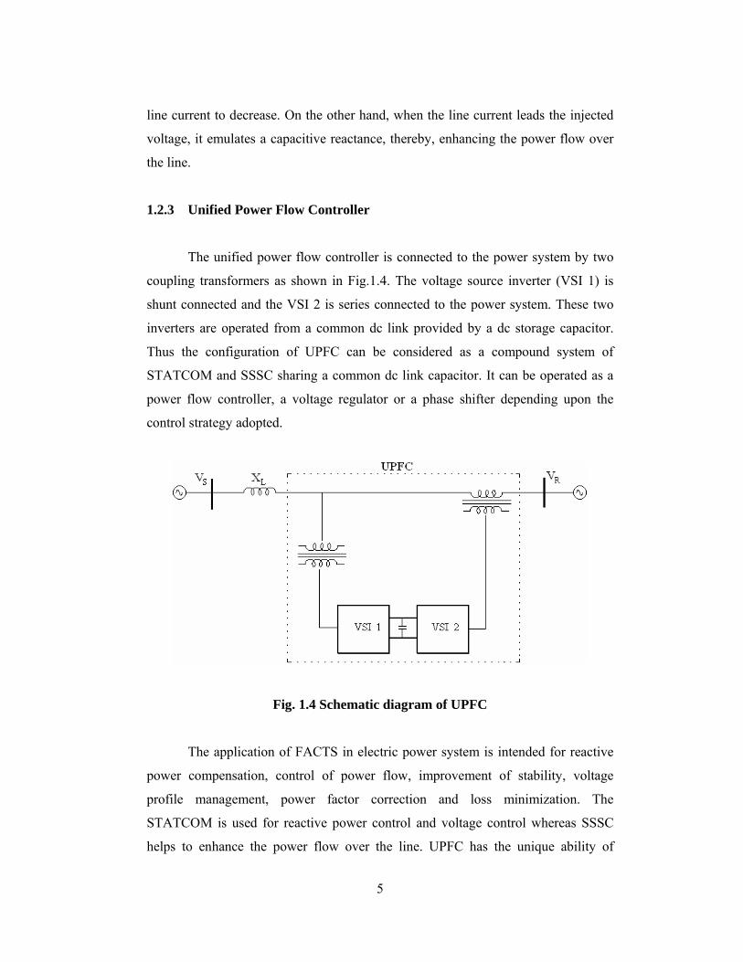
1.2.3 Unified Power Flow Controller
The unified power flow controller is connected to the power system by two
coupling transformers as shown in Fig.1.4. The voltage source inverter (VSI 1) is
shunt connected and the VSI 2 is series connected to the power system. These two
inverters are operated from a common dc link provided by a dc storage capacitor.
Thus the configuration of UPFC can be considered as a compound system of
STATCOM and SSSC sharing a common dc link capacitor. It can be operated as a
power flow controller, a voltage regulator or a phase shifter depending upon the
control strategy adopted.
Fig. 1.4 Schematic diagram of UPFC
The application of FACTS in electric power system is intended for reactive
power compensation, control of power flow, improvement of stability, voltage
profile management, power factor correction and loss minimization. The
STATCOM is used for reactive power control and voltage control whereas SSSC
helps to enhance the power flow over the line. UPFC has the unique ability of

6
controlling the real and reactive power flow independently. Depending on the
desired performance requirement of any utility system, appropriate FACTS
controller has to be identified and incorporated.
1.3 LITERATURE REVIEW
A brief overview of historical background followed by critical review of
earlier investigations carried out on FACTS controllers are presented here.
Controllers in the electric power utility system are very few. Traditionally, they are
implemented in the generating stations to provide power requirements of the
load [4]. They include speed governors; the field exciter systems in the alternators
and the transformer tap changers. In recent times, there is a growing need for more
and better controllers to cope with the many problems related to extensive ac
interconnections, very long distance transmission, congestions in transmission
corridors and power utility deregulation and restructuring.
As ac interconnections multiplied and ac transmission lines stretched over
distances, the effect of distributed line inductance and capacitance manifest
themselves as over voltages during light loads and voltage sags during heavy
loads [25]. There is a need to regulate ac voltages of transmission line. It is done by
var compensation at strategic points, using thyristor switched capacitors (TSC),
thyristor controlled reactors (TCR) and static var compensators (combination of
TCR-TSC) to provide continuous var control [8, 9]. In principle, all shunt type
controllers inject additional current into the system at the point of common coupling.
An impedance of the shunt controller causes a variable current flow and hence
represents an injection of current into the line. As long as the injected current is in
phase quadrature with the line voltage, the shunt controller only supplies or
consumes variable reactive power [26, 27].
In distant ac transmission lines, the increasing inductive reactance reduces
the transient stability limit. The transient stability limit can be raised by series
capacitor compensation with the capacitor controlled by anti-parallel connected

7
thyristors, and was named as thyristor controlled switched capacitor [28, 29]. These
ac power electronic controllers, namely SVC and TCSC, are known as FACTS
controllers [6-8]. In addition, the emergence of switching devices with both turn on
and off capability has led to the development of voltage source inverters. Employing
turn off capability semiconductor devices, switching power converters have been
able to operate at higher switching frequencies and to provide a faster response. This
makes the voltage source inverter an important part in the FACTS controllers [13].
Since the late 1980s, the thyristor based power electronic controllers have found new
embodiments as VSI based FACTS controllers:
• Static var compensator as STATCOM [14, 30, 31].
• Thyristor controlled switched capacitors as SSSC [17, 18].
The STATCOM is the first power converter based shunt connected
controller. The concept of STATCOM [1] was disclosed by Gyugyi in 1986. Again
in 1997, L.Gyugyi et al. made an attempt to describe the operating characteristics of
SSSC in comparison with the thyristor based TCSC [17].
The STATCOM and SSSC are connected back to back with a common dc
link to bring out a new FACTS controller named as unified power flow controller.
With this combination, the UPFC inherits all the benefits of STATCOM and SSSC
and maximize the operational region [20-22, 32, 33]. Several researchers attempted
to study the control and operation of the STATCOM, SSSC and UPFC [18, 34 - 43].
The power circuit of UPFC can be viewed as the conventional ac-dc-ac converter.
This dc link capacitor has inherent disadvantages such as more space requirement, limited
life and also expensive. Besides it slows down the transient response of the circuit [44].
Measures were taken to address the problems of ac-dc-ac conversion when applied for
motor control applications [45-52]. Y. Minari et al. have proposed a scheme of
ac-dc-ac conversion eliminating the electrolytic capacitor [50] in which the rectifier
section has been operated using PWM control to achieve the desired output
waveform. It has been reported that the PWM rectifier/VSI without dc link yields a

8
flexible performance even at low power level. A direct ac-ac energy conversion
device namely the matrix converter (MC) that converts the ac line voltage into
variable voltage arbitrary amplitude, unrestricted frequency without using an
intermediate dc link has been proposed [44, 51, 52]. Similar approaches could be
employed to eliminate the dc link capacitor present in UPFC.
Apart from UPFC, the shunt and the series compensators can also be operated
separately based on the desired compensation. In general, the complete control system of
these FACTS controllers basically consists of two main parts such as external and internal
control. The external control depends on the power system network to which the FACTS
device is connected. However, the internal control mainly depends on the VSI topologies
and should instantaneously respond to a given command, generated by the corresponding
external controller. Different configurations of voltage source inverters can be operated
with the same external control as long as they are connected to the same problematic
network. During the past two decades, exhaustive research was done on external control
of STATCOM [34-37, 53, 54] as well as SSSC [34, 35, 43, 55, 56]. On the other hand,
not much attention was focused on the internal control of the FACTS controllers.
The voltage source inverter, which is a basic building block of these FACTS
devices, generates a sinusoidal output voltage waveform with a desired magnitude
and phase angle demanded by the internal control in synchronism with the
sinusoidal utility system. The traditional two-level VSI produces a square wave
output as it switches the direct voltage source on and off. However for high voltage
applications, a near sinusoidal ac voltage with minimal harmonic distortion is
required. In order to realise higher voltages, each main switch of the 2-level inverter
is formed by connecting many semiconductor devices in a series/parallel fashion. It
is essential that with this arrangement, the electrical and thermal characteristics of
the series and/or parallel connected semiconductor devices should be matched [57].
In response to the growing demand for high power inverter units, multipulse
inverters (MPI) have drawn increased interest in the field of research and industry [58-60].
A multipulse inverter generates a staircase wave closely resembling a sine wave by
9
connecting number of identical three-phase inverter bridges through phase shifting
transformers (PST). The high power STATCOM commissioned at Sullivan
substation, United States used 48-pulse voltage source inverter in order to obtain
higher operating voltages with less harmonic content [1]. Pavel Zuniga-Haro and
Juan M.Ramirez have developed a static synchronous series compensator using
48-pulse voltage source inverter [61]. In this multipulse inverter topology, eight
PSTs are used which are complex and expensive.
An attractive alternative to the multipulse inverter is the multilevel inverter
(MLI) [62-69] which has evolved in three different topologies namely diode
clamped multilevel inverter (DCMLI), [62, 63] flying capacitor multilevel inverter
(FCMLI) [64] and cascaded multilevel inverter (CMLI) [65, 66]. Among the three
configurations, the CMLI with a separate dc capacitor is widely accepted for
applications in high power drives and utility systems due to its modularized circuit
layout and sufficiently high operating voltage [67]. Though the basic concept of the
CMLI has existed over more than two decades, it was not fully realized until
F.Z.Peng and J.S.Lai [65], patented it and presented its various advantages in 1997.
The CMLI consists of a number of H-bridge power conversion cells with each cell
supplied by an isolated source on the dc side and series connected on the ac side so
as to produce a staircase waveform. A premium quality output waveform can be
achieved with a sufficiently high number of voltage levels. However, the number of
voltage levels is limited due to control complexity and cost. Besides, a large number
of dc capacitors are required whose voltages must be balanced in order to avoid
over-voltages on any particular link. The critical review of literature shows neither
MPI nor MLI is useful on their own. A hybrid inverter topology incorporating the
advantages of both MPI and MLI will be attractive. Thus a detailed analysis of
various inverter topologies is absolutely essential in order to propose a suitable
inverter for power system applications.
In recent years, fuzzy logic control (FLC) [70] began to receive more
attention in power systems. However, the investigation on fuzzy applications in
power system control is confined mainly to excitation control and power system

10
stabilizer design [71]. Very few researchers worked on the application of fuzzy
control to FACTS devices [72-77]. In the year 2000, L.O. Mak et al. [73] designed a
fuzzy controller for static synchronous compensator to enhance interconnected
power system stability. They developed fuzzy controller for both main control of
STATCOM and supplementary control to regulate voltage and damp inter-area
power oscillation respectively. In 2003, Stella Morris et al. [74] developed a
variable structure fuzzy control algorithm for controlling the reactive component of
the STATCOM current in a power system.
B.N.Singh et al. [75] have developed a closed loop control schemes for
SSSC with a fuzzy sliding mode controller and fuzzy PI controller to improve the
dynamic response of SSSC. S. Kannan et al. [76] have designed a fuzzy logic
controller as a supplementary controller for SSSC to damp power system oscillation
and improve power system dynamic performance. However, V.K.Chandrakar and
A.G.Kothari [77] have used the fuzzy logic controller as a main controller to control
the magnitude and angle of the SSSC injected voltage operated in voltage injection
mode. In a similar perspective FLC could be used in the closed loop control scheme
of SSSC when operated in other control modes namely line impedance
compensation mode or automatic power flow control (APFC) mode.
Presently, the focus is being directed to understand the behaviour of FACTS
devices in a practical power system. For maximum utilization of any FACTS device
in power system planning, operation and control, power solution of the network with
any of these devices is a fundamental requirement. As a result, substantial research
work has been carried out for developing efficient power flow algorithm for FACTS
devices [78-82].
Power flow studies incorporating UPFC requires an accurate mathematical model
[78, 79]. The model includes algebraic equations, which must be solved iteratively. Most
researchers use Newton – Raphson (N-R) method of iterative solution because of its
quadratic convergence properties. Mihalic R. Zunko [80] et al. introduced a UPFC model
based on a single, ideal series voltage source. H. Ambrez Perez et al. [81],

11
Ghadir Radman and Reshma S. Raje [82] utilizes two ideal voltage sources, one in
series and one in parallel to develop a UPFC steady state model. In 1999, Y.H.Song
et al. [83] proposed a steady state UPFC model and its power injection
transformation had been described in rectangular form. The optimal multiplier
power flow method was applied to implement the UPFC model. A UPFC based
power flow model, derived from two voltage source representations has been
presented in [84]. It is evident from the review of literature that proper methodology
need to be developed for incorporating FACTS devices in the existing three phase
power systems.
1.4 RESEARCH MOTIVATION
With rapid industrialisation and increased standards of living, the demand for
electricity has increased tremendously. The financial and environmental concerns
have prompted to look for ways and means to maximize the utilization of the
available resources and explore measures to enhance the performance of the existing
systems. FACTS devices help to distribute the electrical energy more economically
through better utilization of existing installation, there by reducing the need for
additional transmission lines.
Among the FACTS family, the VSI based FACTS devices have several
advantages such as being small/compact, high response speed and no harmonic
pollution. In the existing scheme of UPFC the key problem is with the dc link
capacitor which is occupying more space, has limited life and also expensive. The
critical review of literature shows that there is ample scope to address the problems
associated with dc link capacitor present in UPFC without compromising its
performance.
The harmonics generated on the ac side of the inverter circuits greatly
influence the power quality of the transmission system. While many benefits may be
realized from large scale introduction of power converters into the power grid, it is
essential to have a detailed analysis on the harmonics generated by these circuits and

12
their impact on power system. It is observed from the critical review of literature
that an exhaustive research work had been carried out in the modeling of these
devices for optimal power flow studies and control analysis. However, much
attention has not been focused on the development of power electronic based
inverter circuits and their control in respect of total harmonic distortion (THD).
Thus, a detailed analysis of various inverter topologies is absolutely essential in
order to propose a suitable inverter for power system applications.
Modern power systems are large, complex, geographically widely distributed
and highly nonlinear. It is not trivial to derive detailed global system model.
Moreover, power system operating conditions and topologies are time varying and
the disturbances are unforeseeable. These uncertainties make it very difficult to
effectively deal with power system stability problems through conventional PI
controller which is based on linearised system model and single operating condition.
The fuzzy logic approach has been emerging in recent years as a complement to the
conventional approach. Thus there is a scope to introduce FLC for enhancing the
dynamic performance of FACTS devices under varying power system operating
conditions. An attempt has been made in the present work to address the aforesaid
issues to improve the performance of VSI based FACTS devices.

13
1.5 OBJECTIVES
The objectives of this dissertation include
i) To build a novel structure of UPFC without dc link capacitor
• To develop suitable modulation techniques and closed loop
control schemes for the series and shunt converters.
• To evaluate its performance and compare with the existing
scheme of UPFC through simulation.
ii) To realize a matrix converter based UPFC, using indirect space
vector modulation (ISVM) technique
• To suggest a suitable closed loop control scheme.
• To study the performance of UPFC with load variations
through simulation.
iii) To develop a STATCOM model using combined multipulse-
multilevel inverter
• To derive a combined multipulse-multilevel inverter
configuration from the existing inverter configurations.
• To construct a closed loop control scheme for operating the
STATCOM in the automatic voltage control (AVC) mode.
• To investigate the performance of the STATCOM under
varying load and fault conditions through simulation.
iv) To design a fuzzy logic controller for SSSC realized through a
combined multipulse-multilevel inverter topology and assess its
performance through simulation in the automatic power flow
control mode under different operating states.
v) To develop a power injection model of UPFC and evaluate its
performance through the standard IEEE -30 bus power system.

14
1.6 THESIS ORGANIZATION
An overview of power electronic converters and the need to identify new
inverter configurations with FACTS devices to improve the performance of power
systems is presented in Chapter 1. Review of literature forms a part of the same
chapter.
The UPFC scheme without dc link capacitor along with the suitable
modulation techniques and closed loop control strategies for the shunt and series
converters are described in Chapter 2. The comparative performance of the proposed
approach with that of the existing scheme is brought out along with the simulation
results. Another scheme of UPFC with matrix converter is realized in the same
chapter. A brief theory of operation of matrix converter along with a suitable
switching strategy and simulation results are explained.
A combined multipulse-multilevel inverter topology suitable for STATCOM
and SSSC applications is proposed in Chapter 3. The performance of the
STATCOM with the proposed inverter configuration and decoupled control strategy
is verified. A detailed discussion on the performance of STATCOM under varying
loads along with the simulation results is presented.
The SSSC is realized with the proposed inverter configuration in Chapter 4.
A detailed elucidation about the fuzzy logic based closed loop controller for
operating the SSSC in the automatic power flow control mode is presented with the
simulation results.
The power injection model for UPFC is developed using Newton’s method
in Chapter 5. The performance of the proposed model is verified through IEEE – 30
bus system by operating the UPFC in its various modes of operation.
The salient features of the work carried out and the major contributions are
summarized in Chapter 6. The scope for further research in the same area is also
outlined.

15
CHAPTER 2
UPFC WITHOUT DC LINK CAPACITOR
2.1 INTRODUCTION
The unified power flow controller, which has been recognized as one of the
best featured FACTS devices [20, 38, 40], is capable of providing simultaneous
active and reactive power flow control, as well as voltage magnitude control.
The UPFC is a combination of static synchronous compensator and static
synchronous series compensator which is connected via a common dc link, to allow
bi-directional flow of real power between series output terminals of SSSC and the
shunt terminals of the STATCOM, and is allowed to provide concurrent real and
reactive power compensation.
The UPFC comprises of two voltage source inverters, operated from a
common dc link provided by a dc storage capacitor. The dc link capacitor should be
properly designed so as to substantially reduce the ripple present in the dc
voltage [57]. The ratings of this dc link capacitor bank pose a significant impact on
the cost and physical size of the UPFC. Besides, this capacitor has shorter life when
compared to ac capacitor of same rating. This in turn limits the life and reliability of
the voltage source inverter [50]. Therefore efforts have to be taken to eliminate the
need of the dc link capacitor and still obtain more or less the same performance. It is
in this pretext two different schemes of UPFC without dc link capacitor have been
proposed.
In the first method the dc link capacitor present in the UPFC is eliminated
and suitable modulation techniques [85, 86] are employed in the converter
configurations so as to operate the UPFC without degrading its performances. The
16
front end converter is operated through a relatively new PWM scheme that enables
to regulate the dc link voltage, minimize the ripples and improve the shape of the dc
link current. Space vector modulation (SVM) strategy is used to fire the switches in
the VSI.
In the second method a matrix converter is employed in UPFC whereby the
classical ac/dc and dc/ac converter structure with dc link capacitor is replaced by a
matrix converter. The indirect space vector modulation technique is used to control
the matrix converter present in the UPFC. The ISVM algorithm for the matrix
converter has the inherent capability of controlling simultaneously both the output
voltage vector and the instantaneous input current displacement angle [87].
The scope includes evaluating the performance of the proposed schemes of UPFC
on a sample power system, in its different operating modes through MATLAB based
simulation and highlights its ability as a powerful voltage regulator and a power
controller.
2.2 POWER SYSTEM WITH THE EXISTING SCHEME OF UPFC
The scheme of UPFC connected with a simple power system is shown in the
Fig. 2.1. UPFC is placed between two sections B2 and B3 of the transmission line.
The feeding network is represented by a Thevenin’s equivalent circuit [88, 89] at
bus B1 where the voltage source is a 230 kV with a short circuit power level of
10,000 MVA and an X/R = 8. The system parameters are given in APPENDIX-A.
The STATCOM model in the UPFC is connected in shunt with the
transmission line using a step-down transformer having leakage reactance XT and a
three phase IGBT based current source rectifier. The ac voltage difference across
this transformer leakage reactance produces reactive power exchange between the
STATCOM and the power system at the point of interface. The voltage can be
regulated to improve the voltage profile of the interconnected power system. Thus
the main function of STATCOM is to regulate the bus voltage magnitude either by
absorbing or generating reactive power to the ac grid network. The SSSC which is

17
connected in series with the transmission line through a series transformer enhances
the power flow over the line by emulating a series capacitance. The capacitance
effect in series with the line is brought by injecting a voltage which is lagging the
line current by 90°.
Fig. 2.1 Power system embedded with a conventional scheme of UPFC
2.3 PROPOSED SCHEME OF UPFC WITHOUT DC LINK CAPACITOR
The elimination of dc link capacitor results in considerable ripple in the dc
link voltage and current distortions in the ac side. To overcome such problems three
capacitors of much smaller rating and lower cost are used in the STATCOM side.
The first converter present in the STATCOM side is operated as a current source
rectifier (CSR) with a suitable pulse width modulation (PWM) technique.
The objectives of this rectifier are to maintain a fixed dc voltage on the dc link
without the dc link capacitor and to regulate the bus voltage. This CSR is connected
in shunt with the transmission line through a coupling transformer. The converter
present in the SSSC is connected in series with the transmission line through a series
insertion transformer. It is controlled using space vector modulation technique to

18
enable it to generate synchronous ac voltage of controllable magnitude and phase
angle with reduced harmonics.
The scheme of ac-dc-ac conversion without dc link capacitor is shown in
Fig.2.2. The filter components R, Lf and Cf present at the input side of the first
converter have a significant role in maintaining the dc link current constant and
reducing the distortions at the transformer and CSR interface. The switching
functions of the current source rectifier and voltage source inverter are adjusted to
maintain the average dc side voltage and current constant [45].
Fig. 2.2 Scheme of ac-dc-ac conversion without dc link capacitor
2.3.1 Modulation Techniques
It is assumed that the ac input voltages to the current source rectifier after the
step down shunt transformer are the three-phase balanced sinusoidal voltages. The
expected line currents in the STATCOM side and the fundamental component of the
line voltages injected into the transmission line in the SSSC side are described as
( )a m i in
b m i in
c m i in
i = I cos ω t - ψ
2πi = I cos ω t - ψ - 32πi = I cos ω t - ψ + 3
⎛ ⎞⎜ ⎟⎝ ⎠⎛ ⎞⎜ ⎟⎝ ⎠
(2.1)

19
where ψin is the STATCOM side power factor angle
su om Tu
sv om Tv om Tu
sw om Tw om Tu
v = V cosθ 2πv = V cosθ = V cos θ - 32πv = V cosθ = V cos θ + 3
⎛ ⎞⎜ ⎟⎝ ⎠⎛ ⎞⎜ ⎟⎝ ⎠
(2.2)
where θTu, θTv and θTw are the angle of the expected output voltage vectors.
A Modified PWM Strategy for the CSR
The dc side voltage of UPFC is essentially decided by the switching function of
the first converter present in the STATCOM and the ac input voltage. In one full cycle of
the ac input there are six switching intervals, during which one of the line or phase
voltages will have the maximum absolute value. For example, in the interval 1, Vsa has the
largest absolute voltage and in the interval 2, Vsc has the largest absolute voltage and so
forth in all the intervals of the three phase sinusoidal voltage of a cycle.
Each switching interval is divided into two portions. During the interval 1,
when Vsa has the largest absolute voltage, T1 is held ON with T6 for the first 30o
conduction period and all other rectifier switches remain in the OFF state. The dc
side voltage is Vdc = Vsa-Vsb. In portion 2, for the next 30o conduction period T1 is
held ON with T2 and all other rectifier switches are OFF. The dc side voltage is
Vdc = Vsa-Vsc. The above sequence is applicable for all other intervals. By
providing this switching sequence, dc voltage at the dc link can be maintained with a
constant value.
Table 2.1 shows the states of the rectifier switches and the dc voltage of each
portion for all the six intervals. Fig.2.3a) and Fig.2.3b) depict the carrier waveform
and the PWM scheme applied to the front end converter using sinusoidal pulse width
modulation (SPWM) technique respectively. The carrier which is initially triangular in
nature slowly changes into ramp and serves to reduce the line side THD. Fig. 2.3c) clearly
depicts the switching pulses applied to the switches present in the converter 1.

20
Table 2.1 Switch state and the dc voltage in each interval
Interval Portion 1 Portion 2 ON switch Vdc ON switch Vdc 1 T1, T6 Vsa- Vsb T1, T2 Vsa - Vsc 2 T2, T1 Vsa - Vsc T2, T3 Vsb - Vsc 3 T3, T2 Vsb - Vsc T3, T4 Vsb - Vsa 4 T4, T3 Vsb - Vsa T4, T5 Vsc - Vsa 5 T5, T4 Vsc - Vsa T5, T6 Vsc - Vsb 6 T6, T5 Vsc- Vsb T6, T1 Vsa - Vsb
Fig. 2.3 a) Carrier signal
Fig. 2.3b) PWM scheme for the first converter

21
Fig. 2.3c) Switching pulses for the first converter
The first converter switches commutate only at the transition between adjacent portions. The switches are made to commutate with zero current by setting zero voltage vector of the inverter to occur at both the beginning and ending of each portion. A separate synchronizing circuit is required [48] to ensure the occurrence of zero voltage vector of the second converter during the commutation of the first converter switches when conventional sinusoidal pulse width modulation technique is employed. However this need for synchronizing circuit can be eliminated if space vector modulation technique is employed instead of sinusoidal pulse width modulation for the second converter.
SVM Strategy for the VSI
Space vector modulation is essentially an averaging technique that takes into consideration that a three-phase inverter has only eight switch states. Each leg has two switch states. Therefore, 23 states can be obtained for the three independent legs of the inverter. The desired three phase voltages at the output of the inverter, operated in the 180° mode can be represented by an equivalent vector Vo rotating in the counter clockwise direction in a two dimensional (d, q) plane as shown in Fig. 2.4. For example, when the desired line to line output voltage vector Vo is in sector 1, it could be synthesized by the pulse-width modulation of the adjacent state space vectors V4(100) and V6(110). The duty cycle of each being d4 and d6 respectively, with the zero vectors V0(000) or V7(111) of duty cycle d0.

22
a m in Tu4 64 6
M 3V cos ψ θd V +d V = 2
(2.3)
d0 = 1-d4-d6
where Ma is the modulation index and 0<Ma <0.866
Using the same theory, analogous vectors and respective duty cycles can be
derived when the system operates in other sectors. The SVM train of pulses applied
to the inverter is as shown in Fig.2.5.
Fig. 2.4 Space vector diagram
Fig. 2.5 SVM pulses applied to the inverter

23
2.3.2 Modes of Operation of the Proposed Scheme of UPFC
Automatic Voltage Control Mode for STATCOM
The controller seen in Fig.2.6 is an integral part of the converter present in
STATCOM to operate it in the automatic voltage control mode. Its function is to
maintain a fixed dc voltage in the dc link without the storage capacitor and ensure
unity power factor in the supply side.
Fig. 2.6 Control block diagram of STATCOM
The reference waveform for the pulse width modulator is derived from the
direct and quadrature components Vd,av and Vq,av respectively. The real power
reference is derived from a dc bus voltage controller and the reactive power is
directly controlled treating iq* as zero, in order to achieve unity power factor
operation [90]. The decoupled control system ensures that a change in the real power
reference can be envisaged without any transient in the reactive power reference and
vice versa. The parameters of the PI controllers used are given in the Table 2.2.
Automatic Power Flow Control Mode for SSSC
The main function of the static synchronous series compensator is to control
the power flow over the transmission line. The control scheme [43] shown in the

24
Fig.2.7 operates the SSSC in the automatic power flow control mode. The reference
inputs (Pref and Qref) are chosen accordingly.
Fig. 2.7 Control block diagram of SSSC
A phase locked loop (PLL) is used to determine the instantaneous angle θ of
the three-phase line voltage Vabc sensed at bus B2 of Fig.2.6. The active and reactive
power flows over the transmission line are determined from the actual line currents
and voltages. Separate PI controllers with optimal values seen in Table 2.2, are used
in the feedback path to regulate the active power and reactive power. The
modulation index Ma to the PWM modulator is derived as
a a a,seM = ΔM M+ (2.4)
where ( )ia p ref act
KΔM = K + P -Ps
⎛ ⎞⎜ ⎟⎝ ⎠
The reference angle θT to the PWM modulator is generated as
Tθ = θ - β (2.5)
where ( )ip ref act
Kβ = K + Q -Q
s⎛ ⎞⎜ ⎟⎝ ⎠
The desired compensation is obtained by either adding or subtracting π/2
with β depending upon whether it is inductive or capacitive. The modulation index
Ma and the phase angle θT are applied to the PWM modulator to generate the SSSC
compensating voltage.

25
Table 2.2 PI controller parameters of the proposed UPFC scheme
PI controllers Kp Ki PI1 0.015 1.6
PI2 0.1 40
STATCOM PI3 0.1 40
PI1 20 2 SSSC
PI2 16 25
2.3.3 Performance Evaluation of the Proposed Scheme of UPFC
Automatic Voltage Control Mode
The proposed model of UPFC is simulated using MATLAB/Simulink.
Fig.2.8 shows the bus voltage and current in the STATCOM side, which are found
to be almost in phase with each other. This explains that the UPFC performs the role
of shunt compensator by either absorbing or supplying the reactive power with the
transmission line. There exists a small phase difference between the bus voltage and
current so as to absorb power from the ac system in order to replenish the operating
losses of the converter.
The THD response of the line current and line voltage in the STATCOM side
given in Figs.2.9 a) and 2.9 b) respectively are found to be very low through a
proper choice of filter components. The dc link voltage and current waveforms of
the proposed scheme of UPFC are compared with that of the existing scheme in
Fig.2.10. Fig.2.11a) shows the distorted dc link current waveform when the dc link
as well as ac capacitors are not present. The steady dc current obtained at the dc link
depicted in Fig.2.11b) emphasizes the necessity of using capacitors on the
ac side.

26
Fig. 2.8 Transmission line voltage and current with UPFC
Fig. 2.9a) Line current THD in the STATCOM side
Fig. 2.9b) Line voltage THD in the STATCOM side

27
a) Existing scheme of UPFC
b) Proposed scheme of UPFC
Fig. 2.10 Comparison of dc link voltage and current

28
a) without AC capacitor
b) with AC capacitor
Fig. 2.11 DC link current of the proposed UPFC scheme
Automatic Power Flow Control Mode
The UPFC is operated with the most powerful control mode namely the
automatic power flow control mode in which the UPFC can directly control the
active and reactive power by controlling the magnitude and angle of the series
injected voltage. The VSI output voltage of the series converter is shown in the
Fig.2.12. This voltage, which is injected in series with the transmission line, lags
the line current almost by 90˚ as seen in Fig.2.13. This reveals that the SSSC
operates in the capacitive mode. The occurrence of a very small deviation of the
injected voltage with respect to the line current is due to the real power losses of the
coupling transformer and the switches in the VSI.

29
Fig.2.12 VSI output voltages with SVM technique
Fig. 2.13 Series injected voltage with respect to transmission line current

30
The transient performance of the system is evaluated by suddenly changing
the load at time t = 0.1 s from an initial value of 300 MW, 220 MVAR to a new
value of 270 MW, 220 MVAR. The variation of P and Q over the line is found to
track almost their reference set values irrespective of load variations as depicted in
Fig.2.14 because of the voltage injected in series at an appropriate angle.
Fig. 2.14 Real and reactive power flow over the transmission line with UPFC
A three-phase fault of 50 ms duration is introduced in the transmission line at
t = 0.2 s and is allowed to be cleared at t = 0.25 s. The voltage across the
STATCOM bus suddenly goes to zero as shown in Fig.2.15a). This results in a
corresponding reduction in dc voltage and current magnitudes and the output of the
VSI present in the SSSC side as depicted in Figs 2.15b) and 2.15c) respectively.
However P and Q of the transmission line settles to their reference values within a
small interval of time once the fault is cleared as seen in Fig. 2.15d).

31
a) Line voltage and current in the STATCOM side
b) DC link voltage and current

32
c) VSI output voltages in the SSSC side
d) Real and reactive power flow over the transmission line
Fig. 2.15 Transient responses for a three-phase fault with UPFC
33
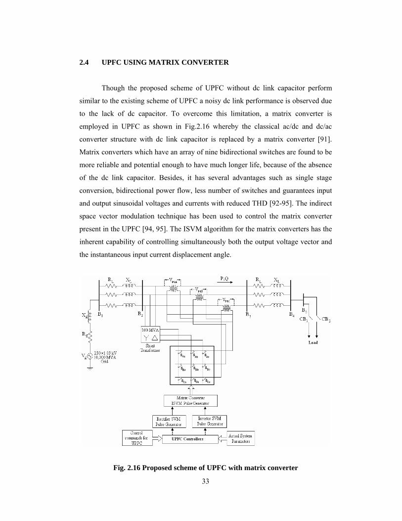
2.4 UPFC USING MATRIX CONVERTER
Though the proposed scheme of UPFC without dc link capacitor perform
similar to the existing scheme of UPFC a noisy dc link performance is observed due
to the lack of dc capacitor. To overcome this limitation, a matrix converter is
employed in UPFC as shown in Fig.2.16 whereby the classical ac/dc and dc/ac
converter structure with dc link capacitor is replaced by a matrix converter [91].
Matrix converters which have an array of nine bidirectional switches are found to be
more reliable and potential enough to have much longer life, because of the absence
of the dc link capacitor. Besides, it has several advantages such as single stage
conversion, bidirectional power flow, less number of switches and guarantees input
and output sinusoidal voltages and currents with reduced THD [92-95]. The indirect
space vector modulation technique has been used to control the matrix converter
present in the UPFC [94, 95]. The ISVM algorithm for the matrix converters has the
inherent capability of controlling simultaneously both the output voltage vector and
the instantaneous input current displacement angle.
Fig. 2.16 Proposed scheme of UPFC with matrix converter

34
2.4.1 Switching Algorithm
In matrix converter, each output phase is connected to each input phase
depending on the state of the switches. Considering that each bidirectional switch is
either in the ON or OFF condition, (29 = 512) different states of the matrix converter
can be defined. For safe operation of the matrix converter input phases should never
be short circuited and output phases should never be opened at any switching time.
Hence the number of allowable switching combination is reduced to 27. Out of
these 27 switching combinations 18 active switching vectors and three zero vectors
are used. The MC switching combination is given in the APPENDIX-B.
In the indirect space vector modulation technique, the matrix converter is
considered as a two stage transformation converter: a rectification stage to provide a
constant imaginary dc link voltage per switching period and an inverter stage to
produce three phase output voltages. However it is only the same nine switches that
perform both rectification and inversion.
Input Current SVM
The SVM uses a combination of two adjacent vectors and a zero vector to
produce the reference current vector as depicted in Fig. 2.17. The input currents can
be considered constant during a short switching interval Ts. Then, for the switching
combination from groups II and III in Appendix-B, the input phase current space
vector is defined as
( )120 12023
−= + +j ji a b ci i i e i e (2.6)
It is assumed that there are only seven discrete positions in the complex
plane, called the input current switching state vectors (SSVs), as shown in Fig.2.17.
For example, if the switching combination 1 from the sub group II-A in the
(APPENDIX–B) is used, the input phase currents are Ia = IA, Ib = 0 and
Ic = -IA, producing the SSV I1 if IA > 0 and I4 if IA < 0 switching combination 4

35
produces the same SSVs but for the opposite polarity of IA. The remaining four
SSVs are produced in a similar manner. All the SSVs have the same magnitude,
which from Fig.2.17 is
k o m2I = I3
kє{1,…6} (2.7)
where om AI = i is the maximum output current
Fig. 2.17 Input current SVM
The desired reference current vector is defined as
i inj(ω t-ψ )in imi = I e (2.8)
where Iim is the maximum input current
ψin is the STATCOM side power factor angle
The input current iin can be approximated by adjacent two switching state
vectors, Iγ and Iδ as shown in Fig.2.18.
Fig. 2.18 Current vector in sector 1

36
The switching combinations from subgroups II-B and II-C produce SSVs in
same positions but with different magnitudes, given by equation (2.7) and by
Iom = ׀iB׀ and Iom = ׀iC׀ respectively. The switching combinations from group III
result in the zero input current SSV I0. The duty cycles of the SSVs are
γγ ai si
S
T πd = = M sin - θT 3
⎛ ⎞⎜ ⎟⎝ ⎠
(2.9)
δδ ai si
S
Td = = M sinθT
(2.10)
zizi γ δ
S
Td = = 1 - d - dT
(2.11)
where Mai is the modulation index of the virtual rectifier stage.
ai0 M 1≤ ≤
imai
om L
2IM =3I cosφ
where Lφ is the displacement angle between the output voltage and current
Output Voltage SVM
The output line voltage space vector is defined as
( )j120 j120o AB BC CA
2V V V e V e3
−= + + (2.12)
which assumes seven discrete positions in the complex plane, as shown in Fig. 2.19.
Fig. 2.19 Output voltage SVM

37
The reference voltage vector is defined as
( )Tj θ + 30o omv = 3 V e
°
(2.13)
This vo can be approximated by two adjacent switching state vectors, Vα and
Vβ and the zero voltage vector Vz using PWM technique as shown in Fig.2.20.
βα zvo α β z
S S S
TT TV = V + V + VT T T
α α β β zv z= d V + d V + d V (2.14)
where Vo is the sampled value of vo at an instant within the switching cycle TS.
The duty cycle of the active switching vectors for the inversion stage Vα and
Vβ are calculated as
α a svπd = M sin - θ3
⎛ ⎞⎜ ⎟⎝ ⎠
(2.15)
β a svd = M sinθ (2.16)
where Ma is the modulation index of the inversion stage a0 M 1≤ ≤
oma
im in
2 VM = 3V cosψ
where Vom is the maximum output voltage
Vim is the maximum input voltage
Fig 2.20 Voltage vector in sector 1

38
A proper balance between the input currents and the output voltages is
obtained in the same switching period. Each switching pattern of the inversion stage
should include both the active sequence of the rectification stage as shown in
Fig.2.21. In the first active portion of the inversion stage, the durations of the
rectification stage active switching vectors are obtained by the following product:
dαγ = dαdγ
dαδ = dα dδ
In second active portion these durations are calculated as follows:
dβγ = dβ dγ
dβδ = dβdδ
Each duty cycle sequence is a result of the product of the rectification and
inversion stage duty cycles. One switching sequence is completed by the zero
vectors with a duty ratio of
( )z αγ αδ βγ βδd = 1- d + d + d + d (2.17)
The duration of each sequence is found by multiplying the corresponding
duty cycle to the switching period.
Fig. 2.21 ISVM switching pattern
Thus in the ISVM method, the four active states and the zero state to be
applied in each PWM period are determined according to the sector in which the
space vectors of output voltage and input current lie. In order to reduce harmonic
distortion, duty cycles are symmetrically distributed round the zero state duty cycle

39
as shown in this figure. The train of pulses obtained using ISVM is shown in
Fig.2.22.
Fig. 2.22 ISVM pulses applied to the matrix converter
2.4.2 Control Scheme of MC based UPFC
The closed loop control scheme shown in Fig.2.23 is an integral part of the
matrix converter present in the UPFC to operate the STATCOM part of the UPFC in
improving the power factor and SSSC part to enhance the power flow over the line.
A single closed control strategy has been used for controlling both the input current
displacement angle as well as the series injected voltage, thereby controlling the
power flow. The references derived separately from the STATCOM and SSSC parts
of the UPFC are combined in the ISVM pulse generator. The ISVM pulse generator
in turn generates appropriate control pulses for the matrix converter switches.
The SSSC control is similar to that described in section 2.3.2.
The parameters of the PI controllers are given in Table 2.3. In the shunt control, in
order to achieve unity power factor the real and reactive power components of the
current must be controlled independently. The real and reactive current references

40
are derived from the instantaneous real and reactive power flow over the line. The
instantaneous real and reactive power can be written in terms of d-q quantities as
( )d d q q3P = V I + V I2
(2.18)
( )d q q d3Q = V I - V I2
(2.19)
From equations (2.18 and 2.19) the real and reactive current references are
derived as follows
ref d ref q*d 2 2
d q
P V + Q V2I = 3 V + V⎛ ⎞⎜ ⎟⎜ ⎟⎝ ⎠
(2.20)
ref q ref d*q 2 2
d q
P V + Q V2I = 3 V + V⎛ ⎞⎜ ⎟⎜ ⎟⎝ ⎠
(2.21)
where Pref is the real power reference
Qref is the reactive power reference
Fig. 2.23 Closed loop control scheme of UPFC with MC
The reactive power reference Qref is set to 0 in order to achieve unity power factor. The derived two phase current commands are converted into three phase quantities using dq-abc transformation. These three phase current references are fed as control signals to the rectifier SVM pulse generator. Similarly the voltage
41
references derived from series control part are fed to the inverter SVM pulse generator. The MC pulse generator uses the control signals from the rectifier and inverter pulse generators for generating appropriate control signals to the matrix converter switches.
Table 2.3 PI controller parameters of the MC based UPFC
PI Controllers Kp Ki
PI1 20 2
PI2 16 25
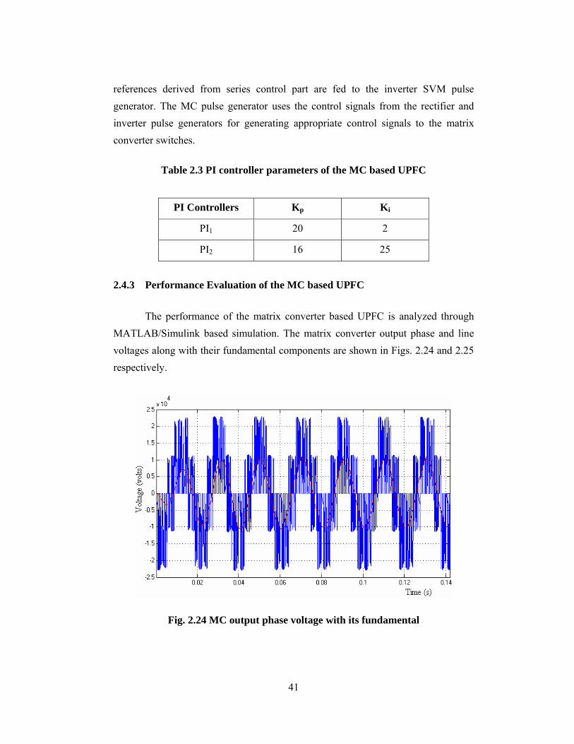
2.4.3 Performance Evaluation of the MC based UPFC
The performance of the matrix converter based UPFC is analyzed through MATLAB/Simulink based simulation. The matrix converter output phase and line voltages along with their fundamental components are shown in Figs. 2.24 and 2.25 respectively.
Fig. 2.24 MC output phase voltage with its fundamental

42
Fig. 2.25 MC output line voltage with its fundamental
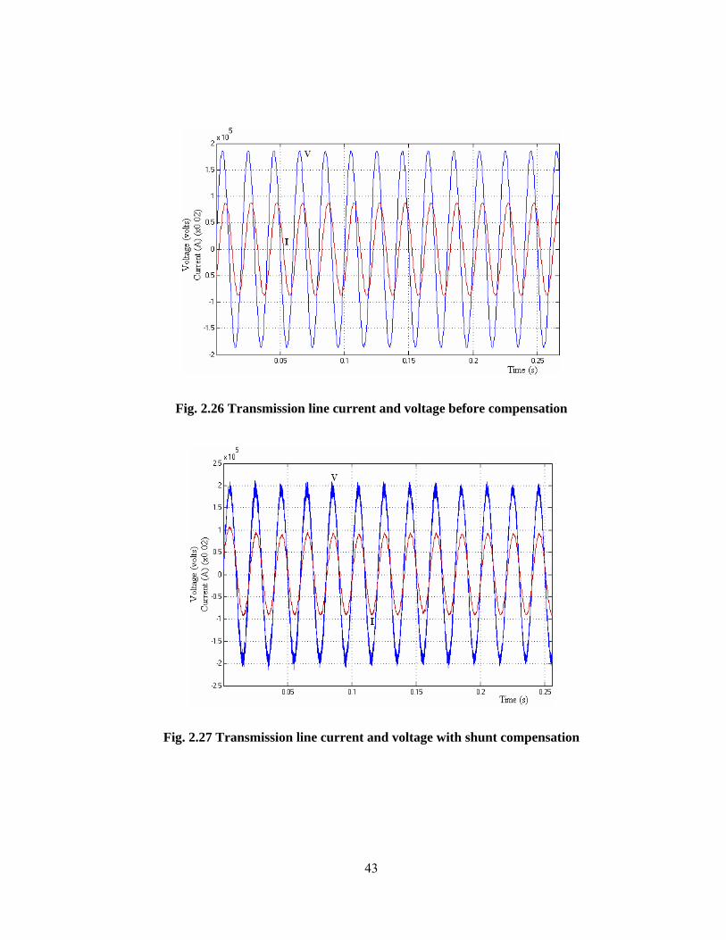
The initial load in the system with the ratings of 600 MW, 150 MVAR
connected at load bus B5 through the circuit breaker CB1 is disconnected at time
t = 0.15 s and a second load with ratings of 650 MW, 200 MVAR is connected to
the system. The transmission line current lags the transmission line voltage as
shown in Fig.2.26 in the absence of UPFC. The STATCOM part of the UPFC
maintains the line current almost in phase with the voltage as depicted in Fig.2.27.
This shows that the UPFC performs the role of shunt compensator by either
absorbing or supplying the reactive power for any load variations.
The magnitude of the quadrature voltage injected by the SSSC depending on
the load variations varies as depicted in the Fig.2.28 in order to maintain the real and
reactive power flow over the line to follow the set reference values as shown in
Fig.2.29.
43
Fig. 2.26 Transmission line current and voltage before compensation
Fig. 2.27 Transmission line current and voltage with shunt compensation

44
Fig. 2.28 Series injected voltage and transmission line current
Fig. 2.29 Real and reactive power flow over the transmission line with MC
based UPFC

45
2.5 SUMMARY
The contribution of this chapter is to propose a novel structure of UPFC to be
connected into the transmission line. Since the cost and space occupied by the dc
link capacitor in the existing UPFC structure are quite large the proposed schemes
eliminate the dc link capacitor. With the proposed scheme 1 a noisy dc link
performance is obtained in the dc link, which is due to the lack of dc capacitor. To
reduce this problem space vector modulation technique is employed for the voltage
source inverter present in the SSSC side. Also another scheme of UPFC is proposed
whereby the classical ac/dc and dc/ac converter structure with dc link capacitor is
replaced by a matrix converter. The indirect space vector modulation technique
effectively used to generate the control pulses for the matrix converter switches.
The performance of the proposed schemes has been analyzed with
MATLAB/Simulink assuming that the UPFC is connected with the 230 kV
transmission line of sample power system. The STATCOM offers a good voltage
regulation and the SSSC controls the magnitude and angle of the injected voltage so
as to maintain the real and reactive power flow over the transmission line to follow
the set reference values in spite of variations in the load and the operating
conditions. The proposed schemes of UPFC interfaced in the sample power system
accomplish a similar performance as that of a traditional system.
46
CHAPTER 3
COMBINED MULTIPULSE MULTILEVEL
INVERTER BASED STATCOM
3.1 INTRODUCTION
Static synchronous compensator is a shunt connected reactive power
compensation device that is capable of generating or absorbing reactive power. The
output voltage of the STATCOM is adjusted to control power factor, regulate
voltage, stabilize power flow and improve the dynamic performance of the power
system. The voltage source inverter is an important part in the STATCOM that
generate a fundamental output voltage waveform with demanded magnitude and
phase angle in synchronism with the sinusoidal system which forces the reactive
power exchange required for compensation.
The traditional two-level VSI produces a square wave output as it switches the direct voltage source on and off. However for high voltage applications, a near sinusoidal ac voltage with minimal harmonic distortion is required. Several high power inverter topologies such as multipulse and multilevel inverters have been proposed for the implementation of FACTS devices.
The key problem with the multipulse inverter is the requirement of magnetic interfaces constituted by complex zig-zag phase shifting transformers which tremendously increases the cost of the complete system [57, 61]. However the multipulse inverter doesn’t have complex control and provides lesser THD. MLI is cheaper than MPI, but requires complex control circuit [57, 96] and produces more THD than MPI. Hence in order to obtain an optimal inverter topology, a trade off between the cost and complexity in control is necessary. Therefore a hybrid topology, involving both multipulse and multilevel inverter configurations extracting the advantages of them will be attractive.

47
3.2 EXISTING 48-PULSE INVERTER TOPOLOGY
In multi-pulse operation, the harmonic content can be significantly reduced
by using several pulses in each half cycle of the output voltage. The 48-pulse
inverter has low harmonic rate on the ac side and can be used for high power
FACTS controllers without ac filters. The 48-pulse inverter is realized by combining
eight 6-pulse voltage source inverters with adequate phase shifts between them. The
configuration of 48-pulse inverter is depicted in the Fig. 3.1 where each of the VSI
output is connected to the phase shifting transformer. Four of them are connected to
a Y-Y transformer and the remaining four to a Δ-Y transformer. The output of the
phase shifting transformers is connected in series to cancel out the lower order
harmonics.
Fig. 3.1 48-pulse voltage source inverter

48
To create a 48-pulse waveform with a harmonic content in the order of
m = 48r±1, (where r = 0, 1, 2,...) the eight 6- pulse inverter voltages need to be phase
shifted. This is implemented by introducing appropriate phase shift in the phase
shifting transformer and the gate pulse pattern of individual VSI. Table 3.1 shows
the phase displacements applied to the gate pulse pattern of each VSI and the
corresponding phase shifting transformer. Thus a premium quality sinusoidal
voltage is obtained with the 48-pulse inverter configuration as depicted in Fig.3.2.
Table 3.1 Phase displacement for a 48-pulse VSI
Coupling transformer
Gate pulse pattern
Phase shifting transformer
Y-Y +11.25˚ -11.25˚
Δ-Y -18.75˚ -11.25˚
Y-Y -3.75 ˚ +3.75˚
Δ-Y -33.75˚ +3.75˚
Y-Y +3.75˚ -3.75˚
Δ-Y -26.25˚ -3.75˚
Y-Y -11.25˚ +11.25˚
Δ-Y -41.25˚ +11.25˚
Fig. 3.2 48-Pulse inverter output voltage

49
It is proposed to build up a forty eight pulse inverter topology through the
twenty four pulse configuration in which each individual two level inverters are
converted to 3-level diode clamped structures. This new topology enjoys the benefits
of both the MPI and MLI configurations and is referred as combined multipulse-
multilevel inverter topology. The harmonic performance of this inverter topology is
evaluated through MATLAB based simulation. It establishes that this structure
almost offers the same response as that of a forty eight pulse inverter in respect of
THD. Further the static synchronous compensator operation is realized using the
proposed high performance, reliable, flexible and cost effective inverter topology.
A closed loop controller based on decoupled control strategy is developed for
effectively operating the STATCOM over a wide range of power system operating
conditions.
3.3 PROPOSED INVERTER TOPOLOGY
The proposed configuration shown in Fig.3.3 is obtained by combining four
three-level diode clamped multilevel inverters with an adequate phase shifts between
them. The voltages generated by each of the three level inverters are applied to the
secondary windings of four different PSTs. Two of them are Y-Y transformers with
a turns ratio of 1:1 and the remaining two are Δ-Y transformers with a turns ratio of 1:√3.
The primary windings of the PSTs are connected in series and the proper pulse pattern as
tabulated in Table 3.2 is maintained so that the fundamental components of the individual
3-level inverters are added in phase on the primary side.
In this configuration the number of PST requirement is reduced to half of
that needed in 48-pusle operation. Though the configuration is similar to a 24-pulse
inverter, it provides very less THD as that of the 48-pulse inverter. This is possible
by selectively eliminating the 23rd and 25th harmonic components through the
appropriate selection of the conduction angle (σ) of the individual three-level
inverter units.

50
Fig. 3.3 Combined multipulse-multilevel inverter
Table 3.2 Phase displacement for the combined multipulse-multilevel inverter
Coupling transformer
Gate pulse pattern
Phase shifting transformer
Y-Y +7.5˚ -7.5˚ Δ-Y -22.5˚ -7.5˚ Y-Y -7.5˚ +7.5˚ Δ-Y -37.5˚ +7.5˚
Each unit in the proposed structure is a diode clamped three-level inverter
configuration as shown in Fig.3.4. The dc-bus voltage is split into three levels by
two series connected bulk capacitors, C1 and C2. The output voltage van has three
states namely Vdc/2, 0 and –Vdc/2 when the switch pairs S1 & S2, S2 & S1′ and
S1′ & S2′ are switched ON respectively. In general the conduction angle σ of the
three level inverter is chosen as
1σ = 180° 1 - m
⎛ ⎞⎜ ⎟⎝ ⎠
(3.1)
where m is the harmonic component which is to be eliminated.

51
Fig. 3.4 Diode clamped 3-level inverter
3.3.1 Harmonic Analysis
The phase-to-phase voltage and the phase-to-neutral voltage of a single three
level diode clamped multilevel inverter with conduction angle σ are described in
Fig. 3.5.
Fig. 3.5 Phase and line voltages of diode clamped 3-level inverter
52
Carrying out the Fourier analysis of the inverter output voltage, the
instantaneous phase-to-neutral voltage is expressed as:
( )man anv t = V sin mωt
m=1
∞∑ (3.2)
where m
DCan
2VV =
mπ
π - σcos m2
⎛ ⎞⎜ ⎟⎝ ⎠
(3.3)
Similarly the instantaneous phase-to-phase voltage is expressed as
( )ab abm
πv t = V sin mωt + m6m=1
∞ ⎛ ⎞∑ ⎜ ⎟
⎝ ⎠ (3.4)
where DCab m
4 V mσ mπV = sin cosmπ 2 6
(3.5)
The voltages vbc(t) and vca(t) exhibit a similar pattern except that they are
phase shifted by 120° and 240° respectively. Similarly the phase voltages vbn(t) and
vcn(t) are also phase shifted by 120° and 240° respectively. It contains only odd
harmonics in the order of 6r±1, where r is a numeral can assume values 1, 2, 3,…..
In general star and delta connected windings have a relative phase shift of
30° and the three-level inverters connected to each of these Y and Δ transformers
will give an overall 12-pulse operation and offers a better harmonic performance.
The output voltage will have a twelve pulse waveform, with harmonics of the order
of 12r±1. Thus the twelve pulse inverter will have 11th, 13th, 23rd, 25th,…..
harmonics with amplitudes of 1/11th, 1/13th, 1/23rd, 1/25th,…… respectively of the
fundamental ac voltage.
The relationship between the phase-to-phase voltage and the phase-to-neutral
voltage is expressed as:
( )mm
rab anv = -1 3 v (3.6)
For obtaining 12-pulse inverter the VSI1 output is connected to a Y-Y
transformer with a 1:1 turn ratio, and the line to neutral voltage using equation (3.6)
can be expressed as:

53
( )( )
abman r1
V1v t = sin mωt3 m=1 -1
∞∑ (3.7)
m = 6r ±1, r = 0,1,2,.....∀
If the VSI2 produces phase-to-phase voltages lagging by 30° with respect to
VSI1 and with the same magnitude, it is given by
( )2 mab abv t = V sin mωt
m=1
∞∑ (3.8)
If this inverter output is connected to a Δ-Y transformer with a 1:1/√3 turn
ratio, the line-to-neutral voltage in the Y-connected secondary will be
( )manY an2
v t = V sin mωtm=1
∞∑ (3.9)
Therefore line-to-line voltage in the secondary side is
( )mabY an2
mπv t = 3V sin mωt +6m=1
∞ ⎛ ⎞∑ ⎜ ⎟
⎝ ⎠ (3.10)
The 12-pulse inverter output is obtained by adding the equations (3.4)
and (3.10).
( ) ( ) ( )ab ab abY12 2v t = v t + v t (3.11)
( )12mab ab12
mπv t = V sin mωt +6m=1
∞ ⎛ ⎞∑ ⎜ ⎟
⎝ ⎠ (3.12)
m = 12r ±1, r = 0,1,2,......∀
since 12m m m mab ab an ab V = V + 3V = 2V
∴ ( )mab ab12
mπv t = 2 V sin mωt +6m=1
∞ ⎛ ⎞∑ ⎜ ⎟
⎝ ⎠ (3.13)
Similarly two twelve pulse inverters phase shifted by 15° from each other
can provide a 24-pulse inverter, with much lower harmonics in the ac side. The ac
output voltage will have 24r±1 order harmonics, i.e., 23rd, 25th, 47th, 49th,…..

54
harmonics, with magnitudes of 1/23rd, 1/25th, 1/47th, 1/49th,…. respectively, of the
fundamental ac voltage. Thus the output voltage of twenty four pulse inverter is
obtained as:
( ) ( )24 m
° °ab abv t = 4 V sin mωt + 22.5 m + 7.5 x
m=1
∞∑ (3.14)
( ) ( )24 m
° °an ab
4v t = V sin mωt + 22.5 m - 22.5 x3 m=1
∞∑ (3.15)
where x = 1 for positive sequence harmonics
x = -1 for negative sequence harmonics
m = 24r ±1, r = 0,1,2,......∀
In order to eliminate the 23rd and 25th harmonic components, the conduction
angle of the inverter is set to σ = 172.5° by choosing m = 24 in equation (3.1). This
configuration produces almost a near sinusoidal output voltage since the lowest
significant harmonic component is the 47th harmonic.
3.3.2 Harmonic Neutralisation
The magnitude and phase angle of the harmonic components present at the
outputs of the diode clamped multilevel inverters VSI1 to VSI4 are given in
Figs.3.6-3.9 respectively. Since the harmonic components 5, 7, 17, 19, 29, 31, 41,
43… present in adjacent inverters (VSI1 and VSI2, VSI3 and VSI4) are out of phase
and have the same magnitude, they cancel each other. Similarly the harmonic
components 11, 13, 35, 37…present in the adjacent pairs of inverters are also
cancelled. The harmonic components 23, 25, 47, 49… which are in phase in all the
four inverters add up with each other. This results to a 24-pulse inverter with the
harmonic components in the order of 24r±1. Fig.3.10 displays the harmonic
components of the 24-pulse inverters.

55
Fig. 3.6 Three level VSI1 harmonics
Fig. 3.7 Three level VSI2 harmonics
Fig. 3.8 Three level VSI3 harmonics

56
Fig. 3.9 Three level VSI4 harmonics
Fig. 3.10 24-pulse inverter harmonics
3.4 REALISATION OF STATCOM OPERATION
The combined multipulse multilevel inverter topology is connected in shunt
with the transmission line using a step-down transformer having leakage reactance
XL as shown in Fig.3.11. The ac voltage difference across this transformer leakage
reactance produces reactive power exchange between the inverter and the power
system at the point of common coupling.

57
Fig. 3.11 Schematic diagram of STATCOM
The magnitude of the inverter output voltage (vs) is controlled to be greater than the voltage (vm) at the PCC in order to operate the inverter in the capacitive mode. In contrast, the magnitude of the output voltage of the inverter is controlled to be less than that of the power system at the PCC when it is desired to absorb the reactive power from the grid [1, 14, 42, 97]. The inverter absorbs a small amount of real power from the ac system to replenish its internal losses and keep the capacitor voltage at the desired level. The losses can be supplied from the ac system by making the output voltage of the inverter lag the ac system voltage by a small
angle φ. This phase difference φ is achieved by adjusting the phase angle of the
sinusoidal modulating signal in SPWM. 3.4.1 STATCOM Model In order to establish the mathematical model of the STATCOM [34, 35, 54, 55] the following assumptions are made:
i) The system parameters and the system voltages are three phase balanced.
ii) All losses in the STATCOM and transformer are represented by an
equivalent resistance R, while the transformer inductance is represented
by an equivalent inductance L.
58
iii) Harmonics produced by the inverter are negligible. Hence the inverter
can be represented by sinusoidal voltage sources.
Fig.3.12 shows the equivalent circuit of the STATCOM connected to the
power system. The reactive power supplied by the STATCOM is either inductive or
capacitive depending upon the relative magnitude of fundamental component of vs
with respect to vm. If |vm| > |vs|, the VSI draws reactive power from the ac bus
whereas if |vm| < |vs|, it supplies reactive power to the ac system.
Fig. 3.12 Equivalent circuit of STATCOM
The equations governing the instantaneous values of the three phase voltages
across the two sides of STATCOM and the current flowing into it are given by
sa sa ma sa
sbsb mb sb
sc
sc mc sc
di -R i v -v0 0dt L
di -R 1 = 0 0 i + v -vdt L L
-Rdi 0 0 i v -vLdt
⎛ ⎞ ⎛ ⎞⎛ ⎞ ⎛ ⎞⎜ ⎟ ⎜ ⎟⎜ ⎟ ⎜ ⎟⎜ ⎟ ⎜ ⎟⎜ ⎟ ⎜ ⎟⎜ ⎟ ⎜ ⎟⎜ ⎟ ⎜ ⎟⎜ ⎟ ⎜ ⎟⎜ ⎟ ⎜ ⎟⎜ ⎟ ⎜ ⎟⎜ ⎟ ⎜ ⎟⎜ ⎟ ⎜ ⎟⎜ ⎟ ⎜ ⎟⎜ ⎟⎜ ⎟ ⎝ ⎠ ⎝ ⎠⎝ ⎠⎝ ⎠
(3.16)
where is is the STATCOM current
Since the system is assumed to be a balanced one, it can be transformed into
a synchronous d-q-o frame by applying Park’s transformation.
59
sdsd md sd
sqsq mq sq
di -R i v -vω 1dt L= +di -R L-ω i v -v
Ldt
⎛ ⎞ ⎛ ⎞⎛ ⎞ ⎛ ⎞⎜ ⎟ ⎜ ⎟⎜ ⎟ ⎜ ⎟⎜ ⎟ ⎜ ⎟⎜ ⎟ ⎜ ⎟⎜ ⎟ ⎜ ⎟⎜ ⎟ ⎜ ⎟⎜ ⎟⎜ ⎟ ⎝ ⎠ ⎝ ⎠⎝ ⎠⎝ ⎠
(3.17)
where ω is the synchronous angular speed of the network voltage.
The power balance equation between the dc and ac terminals of VSI is
( )dc dc sd sd sq sq3P = V I = V I +V I2
(3.18)
Since PWM technique is used in STATCOM, and all the voltage harmonics
produced by the inverter are neglected, the equation relating the dc side and ac side
can be written as
sd a dcV = kM V cosφ (3.19)
sq a dcV = kM V sinφ (3.20)
where sq-1
sd
V= tan
V⎛ ⎞
φ ⎜ ⎟⎝ ⎠
is the angle between the inverter voltage and the system
voltage.
( )2 2
sd sqa
dc
V +VM =
kV is the modulation index of the PWM inverter
k is the ratio between the ac and dc voltage of the inverter
Vdc is the dc voltage
Substituting Vsd and Vsq in equation (3.18)
( )
( )
( )
dc dc a dc sd a dc sq
adc sd sq
dc adc sd sq
3 V I = kM V cos I + kM V sin I23kM
I = I cos + I sin2
dV 3kM = C = I cos + I sin
dt 2
φ φ
∴ φ φ
φ φ
( )dc asd sq
dc
dV 3kM = I cos + I sin
dt 2 C∴ φ φ (3.21)

60
Using equations (3.17) and (3.21), the complete system equation could be
expressed in matrix form as follows:
sd a sd md
sq asq mq
a adc
dcdc dc
di -kM-R i vω cosdt L Ldi -kM-R 1 = ω sin i + vdt L L L
3kM 3kMdV cos sin 0 V 02C 2Cdt
⎛ ⎞⎛ ⎞ ⎛ ⎞ ⎛ ⎞φ⎜ ⎟⎜ ⎟ ⎜ ⎟ ⎜ ⎟⎜ ⎟⎜ ⎟ ⎜ ⎟ ⎜ ⎟⎜ ⎟⎜ ⎟ ⎜ ⎟ ⎜ ⎟φ⎜ ⎟⎜ ⎟ ⎜ ⎟ ⎜ ⎟⎜ ⎟⎜ ⎟ ⎜ ⎟ ⎜ ⎟⎜ ⎟⎜ ⎟ ⎜ ⎟ ⎜ ⎟φ φ⎜ ⎟ ⎜ ⎟ ⎝ ⎠⎝ ⎠⎝ ⎠ ⎝ ⎠
(3.22)
Using equation (3.17), the reference input to the PWM modulator is derived
as follows
sdsd md sq sd
dIV =V + LωI - RI + L
dt⎛ ⎞⎜ ⎟⎝ ⎠
(3.23)
sqsq mq sd sq
dIV =V -LωI - RI + L
dt⎛ ⎞⎜ ⎟⎝ ⎠
(3.24)
The equations (3.23) and (3.24) are realized to establish the STATCOM
operation in the closed loop control scheme.
3.5 CONTROL ALGORITHM FOR STATCOM
A complete closed loop control scheme for operating the realized
STATCOM in the automatic voltage control mode is shown in Fig.3.13. The shunt
converter either absorbs or injects reactive power with the ac grid so as to maintain
the transmission line voltage to a reference value at the PCC. The
injection/absorption of reactive power using STATCOM requires two control loops
namely the outer voltage control loop and the inner reactive current control loop.
The outer dc voltage controller sets the real current reference for the inner current
controller. The reactive current reference is determined by the ac bus voltage
regulator. In the inner current controller a decoupled current control strategy is
employed in order to independently control the real and reactive power components.

61
Fig. 3.13 Closed loop control scheme of STATCOM
A phase locked loop is used to determine the instantaneous angle θ of the
three-phase line voltage Vm sensed at bus B2 of Fig.3.11. The three-phase voltages
sensed at B2 and inverter currents are transformed into two-phase quantities using
Park’s transformation, which gives d – q axis voltage and current for the controller.
The d-axis reference current isd* obtained from the dc voltage controller is compared
with the actual d axis current and stabilized through PI controller to get the
equivalent d axis reference voltage. Similarly the actual q axis current iq is
compared with the reference current isq* derived from the ac voltage controller and
the error so obtained is stabilized through another PI controller to get the equivalent
q axis reference voltage. The parameters of these PI controllers are tuned in order to
minimize the integral square error (ISE) and integral time absolute error (ITAE).
The optimal parameters of PI controllers are tabulated in Table 3.3. Further the
equations (3.23) and (3.24) are realized in the inner current control loop in order to
obtain the reference wave for the PWM modulator.
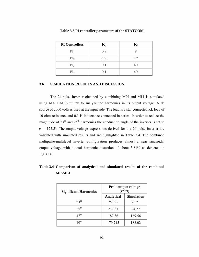
62
Table 3.3 PI controller parameters of the STATCOM
PI Controllers Kp Ki
PI1 0.8 8
PI2 2.56 9.2
PI3 0.1 40
PI4 0.1 40
3.6 SIMULATION RESULTS AND DISCUSSION
The 24-pulse inverter obtained by combining MPI and MLI is simulated
using MATLAB/Simulink to analyze the harmonics in its output voltage. A dc
source of 2000 volts is used at the input side. The load is a star connected RL load of
10 ohm resistance and 0.1 H inductance connected in series. In order to reduce the
magnitude of 23rd and 25th harmonics the conduction angle of the inverter is set to
σ = 172.5°. The output voltage expressions derived for the 24-pulse inverter are
validated with simulated results and are highlighted in Table 3.4. The combined
multipulse-multilevel inverter configuration produces almost a near sinusoidal
output voltage with a total harmonic distortion of about 3.81% as depicted in
Fig.3.14.
Table 3.4 Comparison of analytical and simulated results of the combined
MP-MLI
Peak output voltage (volts) Significant Harmonics
Analytical Simulation 23rd 25.095 25.21
25th 23.087 24.27
47th 187.36 189.56
49th 179.715 183.02

63
a) Output voltage
b) THD
Fig. 3.14 Multipulse-multilevel inverter output voltage and its THD
The same 24-pulse inverter is used to realize the static synchronous
compensator connected to the sample power system described in Fig.3.11. The
steady state and transient response of the system is evaluated through simulation.
3.6.1 Steady State Response
The initial load in the system is with the ratings of P = 300 MW,
QL = 150 MVAR connected at load bus B3 through the circuit breaker CB1.
The transmission line current lags the voltage by 60° as seen in Fig. 3.15 before
t = 0.4 s resulting in a power factor of 0.5 lag and the bus voltage magnitude is at
0.975 pu as the STATCOM is inactive.

64
Fig. 3.15 Transmission line current and voltage with and without STATCOM
At t = 0.4 s, the static synchronous compensator, in the capacitive mode is
connected to the power system network by switching on the circuit breaker CB3. The
STATCOM controller increases the modulation index from 0.74 to 0.778 as shown
in Fig.3.16 in order to increase the voltage magnitude to be higher than the bus
voltage magnitude which enables the injection of 0.24 pu of reactive power into the
ac power system as shown in Fig.3.17.
Fig. 3.16 Variation of modulation index – single load
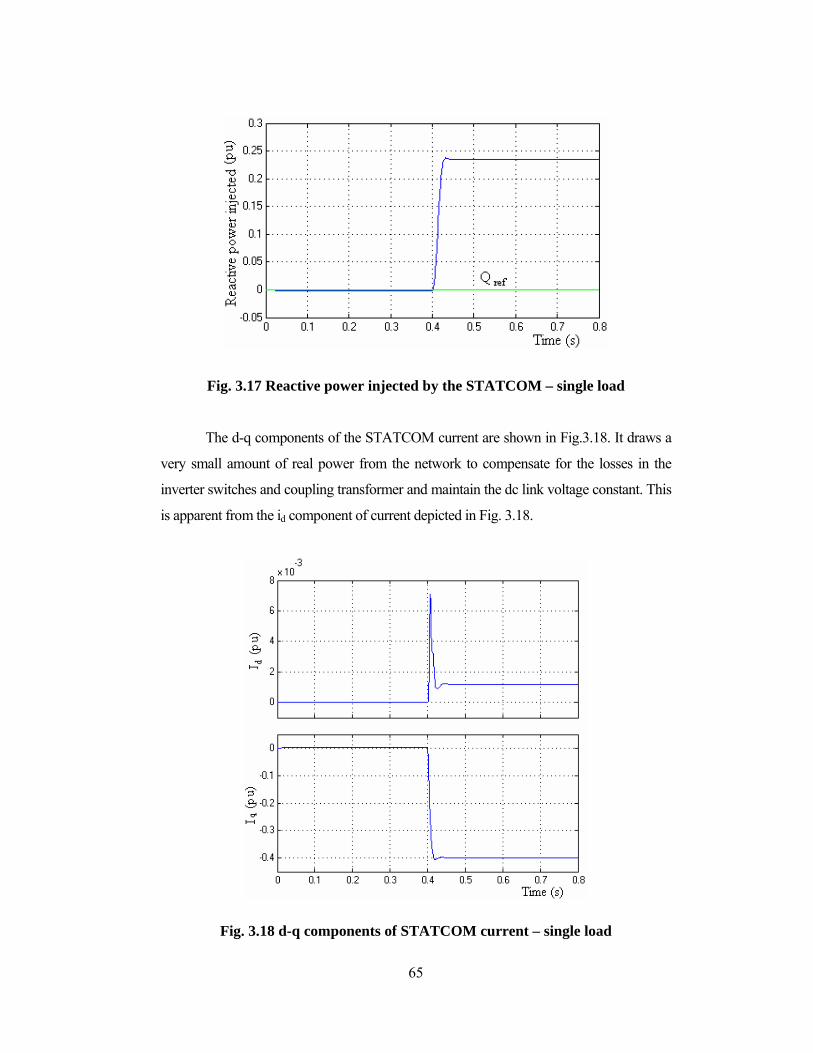
65
Fig. 3.17 Reactive power injected by the STATCOM – single load
The d-q components of the STATCOM current are shown in Fig.3.18. It draws a
very small amount of real power from the network to compensate for the losses in the
inverter switches and coupling transformer and maintain the dc link voltage constant. This
is apparent from the id component of current depicted in Fig. 3.18.
Fig. 3.18 d-q components of STATCOM current – single load

66
The dc link voltage is maintained constant at the desired set reference value
as shown in Fig.3.19. It is observed from the Fig.3.20 that the ac terminal voltage
settles to 1 pu. The phase difference between the transmission line current and the
voltage is reduced to 14.5° as described in Fig.3.15 which improves the power factor
of the line from 0.5 lag to 0.968 lag.
Fig. 3.19 DC side voltage of the inverter – single load
Fig. 3.20 Transmission line voltage – single load

67
3.6.2 Transient Response of the STATCOM under Variable Load
Figs.3.21-3.27 demonstrate the response of the STATCOM when load
variations are introduced at t = 0.4 s and t = 0.6 s respectively. Initially the inductive
Load (P = 300 MW, QL = 150 MVAR) is connected to the bus system through the
circuit breaker CB1. The bus voltage magnitude is 0.975 pu and the phase lag is 60°.
When the STATCOM is switched on at t = 0.2 s, it injects reactive power to the
system thereby increasing the bus voltage magnitude to 0.999 pu and reducing the
power factor to 0.968 lag (φ = 14.5° lag).
An additional inductive load of P = 300 MW, QL = 180 MVAR (Load 2) is
added to the power system at t = 0.4 s by switching ON the circuit breaker CB2. The
new inductive load connected to the bus system requires further reactive power
compensation. Therefore the STATCOM controller increases the modulation index
from 0.778 to 0.83 as shown in Fig.3.21 which provides a total reactive power
injection to 0.49 pu as seen in Fig.3.22. The corresponding variations in the d-q
components of the STATCOM current are clearly depicted in the Fig.3.23. In order
to maintain the dc link voltage to the desired reference value it draws still more real
power from the network and this result an increase in id component of STATCOM
current.
Fig. 3.21 Variation of modulation index under varying load

68
Fig. 3.22 Reactive power injected by the STATCOM under varying load
Fig. 3.23 d-q components of STATCOM current under varying load

69
The bus voltage is regulated to 1.002 pu as in Fig.3.24 and the phase angle is
corrected to 15° lag which leads to a power factor of 0.9659 lag. Thus the line
current is almost in phase with the voltage as depicted in Fig.3.25. The phase angle
difference between the line current and voltage is separately highlighted in Fig.3.26.
Fig. 3.24 Transmission line voltage under varying load
Fig. 3.25 Transmission line voltage and current under varying load

70
Fig. 3.26 Variation of phase angle between the line current and voltage
At t = 0.6 s Load 2 is withdrawn and a capacitive load of P = 300 MW and
QC = 100 MVAR (Load 3) is added to the network in addition to Load 1. Hence
STATCOM injects relatively less amount of reactive power and regulates the bus
voltage to 1.002 pu. The corresponding variations in id and iq are clearly elucidated
in the simulation results. It is evident from Fig.3.27 that the dc link voltage is
maintained constant at the desired set reference value over a wide range of load. The
results are summarized in Table 3.5.
Fig. 3.27 DC side voltage of the inverter under varying load

71
Table 3.5 Dynamic response of STATCOM for load variations
Duration (s)
STATCOM Load Modulation Index (Ma)
Injected Reactive Power,
Qinj (pu)
φ (lag) Bus
Voltage (pu)
0 – 0.2 Not Connected
P = 300MW QL = 150MVAR - - 60° 0.975
0.2-0.4 Connected P = 300MW QL = 150MVAR 0.778 0.24 14.5° 0.999
0.4-0.6 Connected
P = 300MW QL = 150MVAR P = 300MW QL = 180MVAR
0.83 0.49 15.1° 1.002
0.6-0.8 Connected
P = 300MW QL = 150MVAR P = 300MW QC = 100MVAR
0.76 0.13 15.5° 1.002
It is seen from the Fig.3.25 that there is a dip in the supply voltage and the supply currents are lagging. However when the STATCOM is connected to the power system a uniform voltage profile is maintained and the three phase supply currents are almost in phase with the supply voltage under varying load. Hence it is observed from the simulation results that the STATCOM plays a vital role in improving the power factor and regulating the bus voltage. 3.7 SUMMARY A combined multipulse-multilevel inverter topology suitable for high power applications has been proposed. The pulse pattern and the phase shifting transformer arrangement for harmonic neutralization have been discussed in detail. The analytic expressions for the proposed inverter topology are derived using Fourier series and found to closely agree with the simulated results. This new inverter configuration produces almost three phase sinusoidal voltage and maintains THD well below 4%. It has been used to realize the operation of STATCOM and its performance is evaluated through simulation. The closed loop controller based on decoupled control strategy has been developed and found to be effective over a wide range of power system operating conditions.

72
CHAPTER 4
COMBINED MULTIPULSE MULTILEVEL INVERTER
BASED SSSC WITH FLC
4.1 INTRODUCTION
The power flow through a transmission line is a function of line impedance,
voltage magnitude and its phase angle. The most effective way to externally
manipulate such a power flow is by injecting some form of additional series
reactance or acting upon the transmission angle. The former is generally known as
series compensation. The first attempts at series compensation were carried out by
inserting fixed capacitance in series with the line in order to decrease the effective
impedance of the line and therefore increase the power flow through it. The
development of power semiconductor devices has allowed the use of thyristors to
control the series capacitors and inductors for performing continuous control [1].
In addition modern switching devices with turn off capability have led to the
development of voltage source inverters suitable for injecting quadrature voltage in
series with the line, allowing power flow control. This voltage source inverter based
series compensator is one of the FACTS controllers and is referred as static
synchronous series compensator.
In this chapter SSSC is realized using the combined multipulse-multilevel
inverter topology proposed in chapter 3. A closed loop control scheme is developed
to determine the magnitude and appropriate angle at which the voltage is to be
injected and there from control the power flow through the line. The PI regulators
suffer from the inadequacies of providing suitable control under parameter
variations, non-linearity and load disturbances over a wide range of power system
operating conditions. The fuzzy-logic approach [98], on the other hand, provides a

73
model free approach and is suggested for the closed loop control with the view to
enhance the performance of SSSC fed transmission line. The scope includes
evaluating its performance in the automatic power flow control mode through
MATLAB based simulation.
4.2 STATIC SYNCHRONOUS SERIES COMPENSATOR
The static synchronous series compensator is a synchronous voltage source
capable of generating ac voltage of controllable magnitude and phase angle. It
emulates an equivalent inductive or capacitive reactance through a series injection of
voltage, in quadrature with the transmission line current [1, 17, 18]. It serves to
enhance the power flow over the line and accomplish the desired reactive power
compensation. The basic schematic diagram of the static synchronous series
compensator with its test system [89] is shown in Fig.4.1. The specifications of
the test system are given in APPENDIX - C.
Fig. 4.1 230kV sample power system
The sample power system is a 230 kV network equipped with the SSSC
connected in series with the transmission system via series coupling transformer.
The feeding network is represented by a Thevenin’s equivalent circuit at bus B1
where the voltage source is 230 kV with a short circuit power level of 10,000 MVA.

74
The SSSC is placed between two sections B1 and B2 of the transmission line as
shown in this figure. SSSC is rated at ±70 Mvar to provide the required dynamic
series compensation. The compensator is equipped with a combined multipulse-
multilevel inverter, which has the highest performance in providing a nearly
sinusoidal waveform with extremely less total harmonic distortion.
4.3 FUZZY BASED CLOSED LOOP CONTROL SCHEME FOR SSSC
The main function of the static synchronous series compensator is to
dynamically control the power flow over the transmission line. This is possible by
operating the SSSC in the automatic power flow control mode, line impedance
compensation mode, direct voltage injection mode or phase angle regulation
mode [1, 55, 56]. However, the line impedance and automatic power flow modes
are widely employed wherever series compensation is desired. The control scheme
proposed by Anil C. Pradhan and P.W. Lehn [55] is based on the line impedance
control mode in which the SSSC compensating voltage is derived by multiplying the
current amplitude with the desired compensating reactance Xqref. Since it is difficult
to predict Xqref under varying network contingencies, in the proposed scheme, this
controller is modified to operate the static synchronous series compensator in the
automatic power flow control mode.
In this mode the reference input to the controller are Pref and Qref, which are
to be maintained in the transmission line despite of system changes. The
instantaneous real and reactive powers over the transmission line, derived from the
instantaneous power theory [99] is given by
d q d
q d q
V V IP 3 = -V V IQ 2⎛ ⎞⎛ ⎞⎛ ⎞⎜ ⎟⎜ ⎟⎜ ⎟
⎝ ⎠ ⎝ ⎠⎝ ⎠ (4.1)
where P is the instantaneous real power flow over the transmission line
Q is the instantaneous reactive power flow over the transmission line
Vd and Vq are the direct and quadrature components of the transmission line
voltage respectively.

75
Id and Iq are the direct and quadrature components of the transmission line
current respectively.
4.3.1 Fuzzy Logic Controller
The SSSC target is to stabilize the power flow over the transmission line
where it is installed, by properly injecting a quadrature voltage of specified
magnitude and phase angle. The scheme of the fuzzy logic controller is shown in the
Fig.4.2. Two input variables namely the active and reactive power deviations are
given as inputs to the FLC. The controller variables i.e., the output of the FLC is the
required modulation index Ma and the angle β.
Fig. 4.2 Scheme of FLC
Two trapezoidal and five triangular membership functions are chosen for
both input and output variables. There are seven linguistic variables for each input
variable and output variable namely positive large (PL), positive medium (PM),
positive small (PS), zero (Z), negative small (NS), negative medium (NM) and
negative large (NL). The membership functions are asymmetrical because near the
origin, the signals require more precision. The adopted membership functions for the
active power deviation and reactive power deviation are depicted in Figs. 4.3 and 4.4
respectively.
76
Fig. 4.3 Adopted membership functions for active power deviation
Fig. 4.4 Adopted membership functions for reactive power deviation

77
The control decisions are made on the basis of fuzzified linguistic variables.
There are 49 (7×7) rules for a system with two control variables and seven linguistic
variables as seen in Table 4.1. The min-max inference is applied to determine the
degree of memberships for output variables. Defuzzification of fuzzy decision
inferred from the fired rules is done using bisector method.
Table 4.1 Rule table
Error
PL PM PS Z NS NM NL
NL PL PL PL PM PM PS Z
NM PL PL PM PM PS Z NS
NS PL PM PS PS Z NS NM
Z PL PM PS Z NS NM NL
PS PM PS Z NS NS NM NL
PM PS Z NS NM NM NL NL
Cha
nge
in e
rror
PL Z NS NM NM NL NL NL
4.3.2 Closed Loop Control
In the closed loop control scheme shown in Fig.4.5, the three phase voltages
and currents sensed at B2 of transmission line (Fig.4.1) are transformed into
two-phase quantities using Park’s transformation, which gives d-q axis currents and
voltages for the controller. The actual real and reactive powers are calculated from
these d-q components of currents and voltages, using equation (4.1) and compared
with the desired Pref and Qref respectively. The error components Perr and Qerr so
obtained are stabilized through the fuzzy logic controller. The desired modulation
index Ma of the PWM modulator is derived from the active power control part of the
circuit. The reference angle θT to the PWM modulator is obtained as described in the
phasor diagram [55] of Fig.4.6.

78
Fig. 4.5 SSSC closed loop control
Fig. 4.6 Phasor diagram of the controller

79
A phase locked loop is used to determine the instantaneous angle θ of the three
phase voltage vabc sensed at B2 (Fig.4.1). The current components Id and Iq are used to
determine the amplitude of the current⏐I⏐and its angle relative to vabc, called θir.
The required SSSC injected voltage angle is derived as follows:
T irπθ = θ - θ β2
± ± (4.2)
where θ is the instantaneous angle of the line voltage
θir is the angle between the line voltage and line current
β is the small perturbation added to the inverter voltage angle needed to
charge or discharge the capacitor voltage
The angle ±π/2 is included in (4.2), to enable the quadrature injection of
voltage with respect to line current. The angle β is derived from the reactive power
control part of the circuit. Using the modulation index Ma and the angle θT, the three
phase reference values of the injected voltage are expressed as *
Ta a T*
Tb a T*
Tc a T
V = M sinθ
V = M sin(θ + 2π 3)
V = M sin(θ -2π 3)
(4.3)
where VT is the quadrature voltage injected in series with the line current.
These reference waveforms are used in the PWM modulator to generate the
control pulses for the inverter switches.
4.4 SIMULATION RESULTS AND DISCUSSION
The performance of SSSC is evaluated through MATLAB based simulation,
when it is operated in the automatic power flow control mode.
4.4.1 Steady State Response of SSSC
The initial load in the system is Load 1 with the ratings of P = 300 MW, Q = 100 MVAR connected at load bus B3 through the circuit breaker CB1. In order to
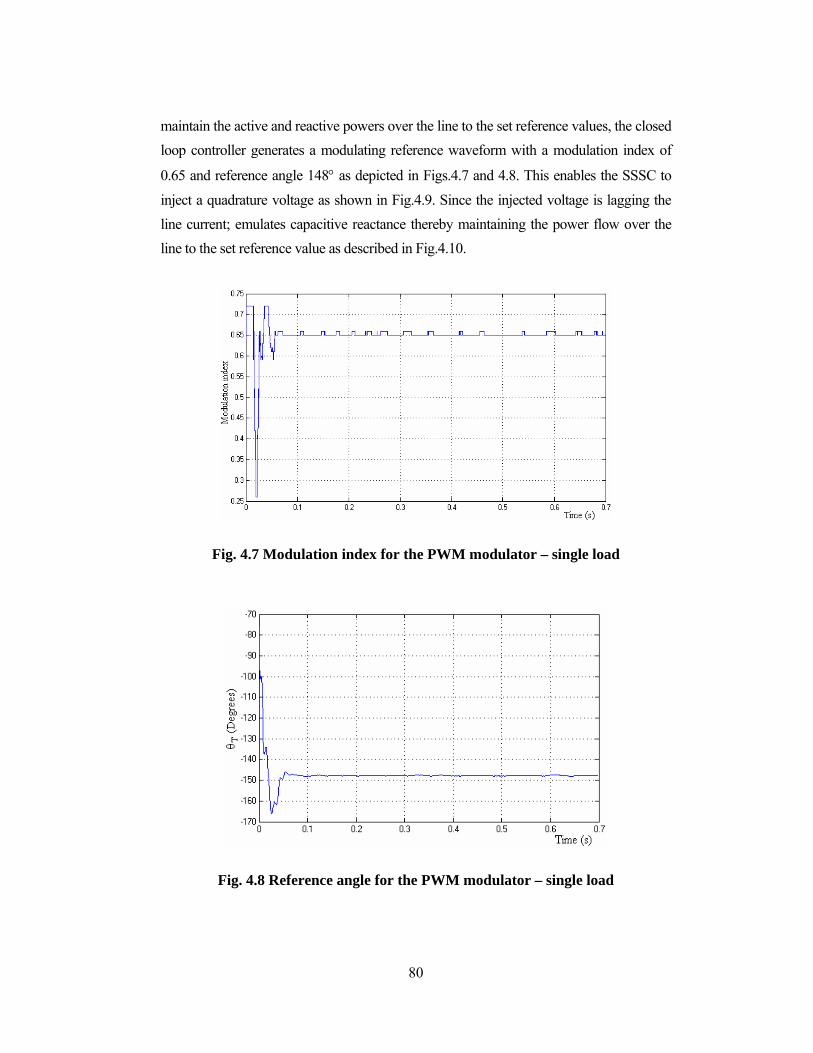
80
maintain the active and reactive powers over the line to the set reference values, the closed loop controller generates a modulating reference waveform with a modulation index of
0.65 and reference angle 148° as depicted in Figs.4.7 and 4.8. This enables the SSSC to inject a quadrature voltage as shown in Fig.4.9. Since the injected voltage is lagging the line current; emulates capacitive reactance thereby maintaining the power flow over the line to the set reference value as described in Fig.4.10.
Fig. 4.7 Modulation index for the PWM modulator – single load
Fig. 4.8 Reference angle for the PWM modulator – single load

81
Fig. 4.9 SSSC injected voltage and transmission line current – single load
Fig. 4.10 Real and reactive power flow over the line – single load

82
4.4.2 Transient Response of SSC under Variable Load
The various transient disturbances due to faults and load variations are created to
study the performance of the fuzzy logic controller for SSSC. The initial load in the
system is Load 1 with the ratings of P = 350 MW, Q = 75 MVAR and is disconnected at
time t = 0.3 s and Load 2 with ratings of P = 400 MW, QL = 100 MVAR is connected to
the system. The transmission line current is lagging the line voltage by an angle θir as
shown in Fig.4.11. The phase angle difference between the line current and voltage is
separately highlighted in Fig.4.12. Based on the angle θir and the amount of desired real
and reactive power flow over the transmission line, the closed loop controller generates a
modulating reference waveform to the PWM modulator. The variations of the modulation
index (Ma) and the reference angle (θT) of the PWM modulator are depicted in Figs.4.13
and 4.14 respectively for the load variation given at t = 0.3 s.
Fig. 4.11Transmission line voltage and current under varying load

83
Fig. 4.12 Phase angle between line current and voltage
Fig. 4.13 Modulation index under varying load

84
Fig. 4.14 Reference angle for the PWM modulator under varying load
Using the reference angle and modulation index the voltage source inverter
generates voltage of desired magnitude and phase angle, and is injected in series
with the transmission line as shown in Fig.4.15. This series injected voltage lags the
line current by an angle (δ) less than 90˚ as described in Fig.4.16 and thereby
provides capacitive compensation.
The series injected voltage with desired magnitude and angle enables the
active and reactive power of the transmission line to track the set reference values
namely Pref = 0.6 pu and Qref = 0.25 pu irrespective of load variations as depicted in
Fig.4.17. However with PI controller for the same load variation given at t = 0.3 s,
the real and reactive power do not follow the set reference values. The real power
reduces to 0.55 pu and reactive power enhances to 0.27 pu as shown in the Fig.4.18.
This proves the robustness of the fuzzy logic controller over the conventional
PI controller.

85
Fig. 4.15 SSSC injected voltage and transmission line current under varying load
Fig. 4.16 Phase angle between the line current and injected voltage

86
Fig. 4.17 Real and reactive power flow over the line with FLC
Fig. 4.18 Real and reactive power flow over the line with PI controller

87
In addition the system performance is evaluated when a three phase fault is
applied at t = 0.3 s and cleared at t = 0.35 s as described in Fig.4.19. P and Q of the
transmission line settle to the reference values within a small interval of time after the fault
is cleared and this proves the transient stability of the proposed FLC for SSSC.
Fig. 4.19 Real and reactive power flow over the line for a three phase fault
4.5 SUMMARY
A combined multipulse-multilevel inverter has been operated suitably to depict the
behaviour of SSSC. A closed loop fuzzy logic control scheme has been developed
for operating the SSSC in the automatic power flow control mode. The parameters
of the fuzzy controller have been varied widely by a suitable choice of membership
functions and parameters in the rule base.
It is inferred from the results that the FLC is a viable controller for the SSSC
in order to maintain the real and reactive power flow over the transmission line to
follow the set reference values under a variety of transient disturbances including
high and low load conditions.

88
CHAPTER 5
POWER FLOW MODELING AND ANALYSIS OF UPFC
5.1 INTRODUCTION
The industrial growth of a nation necessitates an urgent need for higher
exchange of electrical energy through the existing transmission lines. The
transmission lines are therefore expected to be operated at their maximum capacity.
Efforts are necessary to raise and control the power flow in the system without
losing its reliability. The traditional power flow algorithms appear to be inadequate
to meet the growing challenges and bring out the need for improved strategies.
The growth of solid state technology along with the development of fast
acting switches has paved the way for the era of power electronic based
compensators known as FACTS. The objective of these devices is to provide
reactive shunt compensation in a transmission system with a view to increase the
transmittable power capability from generation to the load, which serves to improve
the steady state characteristics as well as the stability of the system.
A UPFC constituted using two power electronic converters namely a series
converter and a shunt converter cascaded through a common dc link can be operated
as a power flow controller, a voltage regulator or a phase shifter depending upon the
adopted control strategy. The computation and control of power flow for system
embedded with UPFC is a significant requirement in the present day automated
world [81] to provide a scope for effective planning and operation.
It is acknowledged that the system output voltage deteriorates primarily due
to the inability of the system to supply adequate reactive power. Besides, it further

89
limits the power transfer capability and more often does not meet the demand.
Therefore there is a definite need to develop methods that serve to enhance the
voltage magnitude and increase the allowable flow of power through the line. It is in
this context an algorithm is developed using UPFC and evaluated through a standard
IEEE 30-bus system.
5.2 PROPOSED ALGORITHM
The UPFC injection model is derived enabling three parameters to be
simultaneously controlled. They are namely the shunt reactive power Qinj, the
magnitude VT, and the angle θT of the injected series voltage. Fig.5.1 shows the
model of a UPFC connected to link k-m of an N-Bus power system. The
STATCOM is assumed to operate in the voltage control mode which means that the
STATCOM absorbs proper amount of reactive power from the power system to
keep kV constant for all power system loading within reasonable range. The SSSC
is operated in automatic power flow control mode and modelled as voltage source
VT with adjustable magnitude and angle θT with impedance Zse. Hence the
admittance matrix of the system is modified to include the series source impedance.
This is done by changing the line impedance between bus k and bus m such that
( ) ( )km se seZ R R j X X= + + +
and hence km km kmkm
1Y G jBZ
= = +
Fig. 5.1 Circuit model of UPFC
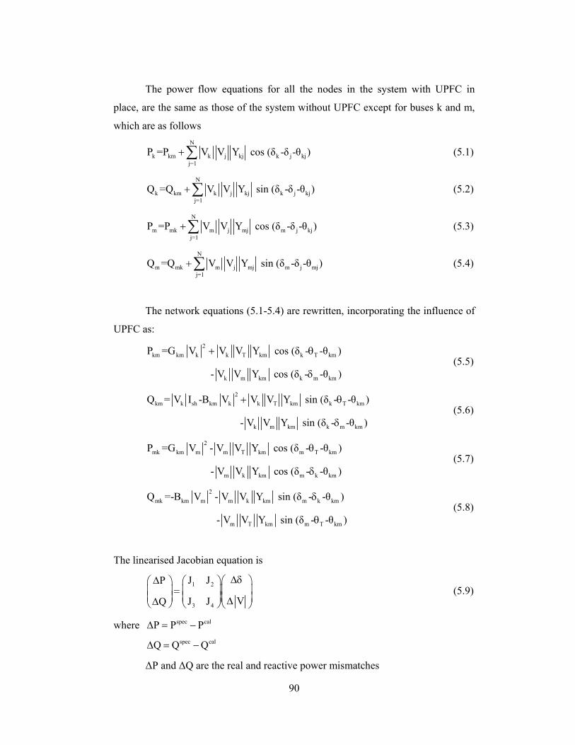
90
The power flow equations for all the nodes in the system with UPFC in
place, are the same as those of the system without UPFC except for buses k and m,
which are as follows N
k km k j kj k j kjj=1
P =P V V Y cos (δ -δ -θ )+∑ (5.1)
N
k km k j kj k j kjj=1
Q =Q V V Y sin (δ -δ -θ )+∑ (5.2)
N
m mk m j mj m j kjj=1
P =P V V Y cos (δ -δ -θ )+∑ (5.3)
N
m mk m j mj m j mjj=1
Q =Q V V Y sin (δ -δ -θ )+∑ (5.4)
The network equations (5.1-5.4) are rewritten, incorporating the influence of
UPFC as: 2
km km k k T km k T km
k m km k m km
P =G V V V Y cos (δ - -θ )
- V V Y cos (δ - -θ )
+ θ
δ (5.5)
2km k sh km k k T km k T km
k m km k m km
Q = V I -B V V V Y sin (δ - -θ )
- V V Y sin (δ - -θ )
+ θ
δ (5.6)
2mk km m m T km m T km
m k km m k km
P =G V - V V Y cos (δ - -θ )
- V V Y cos (δ - -θ )
θ
δ (5.7)
2
mk km m m k km m k km
m T km m T km
Q =-B V - V V Y sin (δ - -θ )
- V V Y sin (δ - -θ )
δ
θ (5.8)
The linearised Jacobian equation is
1 2
3 4
J JP
VJ JQ
ΔδΔ ⎛ ⎞⎛ ⎞⎛ ⎞⎜ ⎟⎜ ⎟=⎜ ⎟⎜ ⎟ ⎜ ⎟⎜ ⎟ΔΔ⎝ ⎠ ⎝ ⎠⎝ ⎠
(5.9)
where spec calP P PΔ = −
spec calQ Q QΔ = −
ΔP and ΔQ are the real and reactive power mismatches

91
Δδ and Δ׀V׀ are the errors in phase angles and magnitudes of the voltage to
be minimized.
J1-J4 are the partial derivatives of ΔP and ΔQ with respect to Δδ and ΔV
respectively.
The equations (5.5-5.8) are inserted in the above equation as follows
old new
PJ J
V VQ
Δδ ΔδΔ ⎛ ⎞ ⎛ ⎞⎛ ⎞⎜ ⎟ ⎜ ⎟= +⎜ ⎟⎜ ⎟ ⎜ ⎟ ⎜ ⎟Δ ΔΔ⎝ ⎠ ⎝ ⎠ ⎝ ⎠
(5.10)
where Jold is the normal N-R power flow Jacobian matrix.
Jnew is the partial derivative matrix of the UPFC injected power with respect
to the variables.
The elements of Jnew are described below:
kmk T km k T km
k
k m km k m km
PV V Y sin (δ - -θ )
+ V V Y sin (δ - -θ )
∂= − θ
∂δ
δ
(5.11)
kmk m km k m km
m
P V V Y sin (δ - -θ )∂= − δ
∂δ (5.12)
kmkm k T km k T km
k
m km k m km
P = 2G V V Y cos (δ - -θ )
V
- V Y cos (δ - -θ )
∂+ θ
∂
δ
(5.13)
kmk km k m km
m
P = - V Y cos (δ - -θ )V
∂δ
∂ (5.14)
km
k T km k T kmk
k m km k m km
QV V Y cos (δ - -θ )
- V V Y cos (δ - -θ )
∂= θ
∂δ
δ
(5.15)
kmk m km k m km
m
Q V V Y cos (δ - -θ )∂= δ
∂δ (5.16)

92
kmsh km k T km k T km
k
m km k m km
Q = I -2B V V Y sin (δ - -θ )
V
- V Y sin (δ - -θ )
∂+ θ
∂
δ
(5.17)
kmk km k m km
m
Q = - V Y sin (δ - -θ )V
∂δ
∂ (5.18)
mkm k km m k km
k
P V V Y sin (δ - -θ )∂= − δ
∂δ (5.19)
mkm k km m k km
m
m T km m T km
PV V Y sin (δ - -θ )
V V Y sin (δ - -θ )
∂= δ
∂δ
+ θ
(5.20)
mkm km m k km
k
P = - V Y cos (δ - -θ )V
∂δ
∂ (5.21)
mkk km m k km
m
m T km m T km
P = - V Y cos (δ - -θ )
V
- V V Y cos (δ - -θ )
∂δ
∂
θ
(5.22)
mkm k km m k km
k
Q = V V Y cos (δ - -θ )∂δ
∂δ (5.23)
mkm k km m k km
m
m T km m T km
Q- V V Y cos (δ - -θ )
- V V Y cos (δ - -θ )
∂= δ
∂δ
θ
(5.24)
mkm km m k km
k
Q = - V Y sin (δ - -θ )V
∂δ
∂ (5.25)
mk
km m k km m k kmm
T km m T km
Q-2B V V Y sin (δ - -θ )
V
- V Y sin (δ - -θ )
∂= − δ
∂
θ
(5.26)
With the help of equations (5.11 – 5.26) the power flow Jacobian matrix is
modified and the power flow solution is obtained using N-R method. The flowchart
of the proposed power flow algorithm is shown in Fig.5.2.

93
Fig. 5.2 Flowchart of the power flow algorithm
5.2.1 Line Identification
It is essential to locate the UPFC optimally in a power system. The optimal
placement of UPFC in the transmission system is determined using the performance
index (PI) given in the equation (5.27).
m
2ni-j
i-jmax
WPI2n
S =
S⎛ ⎞⎜ ⎟⎜ ⎟⎝ ⎠
(5.27)
where Si-j is the apparent power flow in the line i-j.
Si-jmax is the maximum rated capacity of the line i-j.

94
n is the exponent and taken as 1.
Wm is a real nonnegative weighing coefficient.
PI is small when the line flows are within their limits and attains a high value
when there are overloads [100]. Thus it provides a good measure of severity of the
line overloads for a given state of the power system.
5.3 SIMULATION STUDIES
The feasibility of the proposed technique is investigated by conducting
power flow studies on IEEE 30-bus system [101]. The system data are given in
APPENDIX – D. The value of PI is determined from the equation (5.27) using the
power flows and de-rated limits of the transmission lines. The branches ranked
according to their corresponding PI values, are tabulated in the Table5.1*.
Table 5.1 Ranking of branches for IEEE 30-bus system
Rank Line Number Between Buses PI 1 33 24-25 0.0053 2 20 14-15 0.0072
3 39 29-30 0.0104
4 40 8-28 0.0140
5 35 25-27 0.0142
6 22 15-18 0.0176
7 32 23-24 0.0181
8 11 6-9 0.0209
9 26 10-17 0.0220
10 36 28-27 0.0320
11 17 12-14 0.0347
12 34 25-26 0.0354
13 12 6-10 0.0366 * Remaining branches which have higher PI value are not tabulated

95
It is evident that the UPFC can be operated in different modes to suit specific
requirements. The structure of UPFC can be tailor made to function in different
constituent entities, without in any way affecting the operation of the system. It can
be either independently operated as STATCOM/SSSC or made to function in a
combined STATCOM/SSSC form. The various modes of operation are:
Case I: Power flow control mode (STATCOM disabled and SSSC enabled)
Case II: Voltage control mode (STATCOM enabled and SSSC disabled)
Case III: Simultaneous control of voltage and power flow (both STATCOM
and SSSC enabled).
5.3.1 Case I: Power Flow Control Mode
The objective of UPFC when operated in SSSC mode is to control the active
power flow between two buses. Table 5.1 shows that the line 33 between buses 24
and 25 is less loaded and hence has the least performance index. The line 33 is
chosen as the best location to place the UPFC when it is operated in the power flow
control mode (STATCOM disabled) for active power enhancement. Uncompensated
real and reactive power flow on line L-33 are 1.543 MW and 0.572 MVAR
respectively, while the total real and reactive transmission losses are 7.616 MW
and -17.125 MVAR respectively.
When the UPFC is incorporated in L-33, the total power loss of the system is
reduced to 6.237 MW i.e. reduced approximately by 18%. Fig. 5.3 shows the real
power regulation of line L-33 against variations in the series injected voltage and its
angle for a fixed value of Ish = 0 (STATCOM inhibited). The series injected voltage
is varied in a rotational manner having constant magnitude VT = 0.03 pu and varying
the angle Tθ between 0° and 360°. Upon completion of a full circle of the angle Tθ ,
the magnitude VT is changed in steps of 0.01pu up to 0.1pu.

96
Fig. 5.3 Power flow over the line L-33
The power flow in the line is 1.543 MW without UPFC. By inserting
maximum value of the magnitude VT (0.1pu), the active power can be increased to
2.762 MW, if the angle Tθ is appropriately adjusted. The maximum active power
flow condition occurs at around 86°. Fig. 5.4a) depicts the active power flow over
each line of the bus system under consideration with and without the UPFC. It is
seen that the real power is significantly improved in the line L-33 since the UPFC is
connected to that line along with enhancement in some other lines. The enhancement
of power flow in the line L-33 is separately highlighted in the Fig. 5.4b). These
results are obtained over a small variation of bus voltages.

97
0 5 10 15 20 25 30 35 40 45
-20
0
20
40
60
80
100
Line Number
Act
ive
pow
er fl
ow (M
W)
Without UPFCWith UPFC
Fig. 5.4a) Active power flow in 30-Bus system with and without UPFC – PFC mode
Fig. 5.4b) Active power flow in L-33 with and without UPFC – PFC mode

98
5.3.2 Case II: Voltage Control Mode
The focus of UPFC when operated in STATCOM mode is to regulate the bus
voltage under light and heavy load conditions. To identify the location of UPFC
when operated in voltage control mode (SSSC disabled), apart from PI calculations
the buses having voltage profile out of acceptable limits (0.95 pu < VB < 1.05 pu)
need to be considered. The voltage of the load bus 12 shoots up to 1.062 pu without
FACTS device and it is desired to regulate the voltage of bus 12 at 1.00 pu under all
operating conditions. Hence the developed UPFC model (with SSSC disabled) is
incorporated in the Line 17 between bus 12 and bus 14. The voltage of the bus 12 is
reduced from 1.06 pu to 1.0 pu, which is 5.6% drop after incorporating the FACTS
device. The shunt compensator absorbs an inductive current of 0.24 pu.
The voltage profile of the load buses with and without UPFC is shown in
Fig.5.5. The voltages at the load buses 9 and 12 were out of acceptable
limits (>1.05 pu) without UPFC and are regulated nearer to unity with the UPFC
installed along with a noticeable regulation in most of the load buses.
0 5 10 15 20 25 300.8
0.85
0.9
0.95
1
1.05
1.1
1.15
Bus Number
Without UPFCWith UPFC
Fig. 5.5 Bus voltage at each load bus of IEEE 30-Bus system with and without
UPFC – VC mode

99
5.3.3 Case III: Simultaneous Control of Voltage and Power Flow
The best location for UPFC when operated in both voltage control mode and
power flow control mode is in the line 20 between the buses 14 and 15. Because the
line 14-15 (L-20) is less loaded, it has relatively lesser performance index and the
corresponding bus voltages shoot up.
Uncompensated real and reactive power flow in the line L-20 are1.835 MW
and 0.549 MVAR respectively, while the total real and reactive transmission losses
are 7.616 MW and -17.125 MVAR respectively. When UPFC is incorporated in
L-20, the total power loss of the system is reduced to 5.812 MW ie reduced
approximately by 24%. The UPFC injects a voltage of 0.1 pu at an angle of 86° and
absorbs inductive current of 0.132 pu.
Fig. 5.6a) depicts the active power flow over each line of the bus system
under consideration with and without UPFC. It is seen that the real power is
enhanced in most of the lines and the enhancement is significant in the line L-20
since UPFC is connected to that line. The enhancement of power flow in the line
L-20 is separately highlighted in the Fig. 5.6b).
The voltage profile of the load buses with and without UPFC is shown in
Fig.5.7. The voltage of the bus 14 is reduced from 1.047 pu to 1.035 pu and that of
15 is reduced from 1.042 pu to 1.0277 pu, after incorporating the FACTS device.
The voltages at the load buses 9 and 12 are out of acceptable limits (>1.05 pu)
without UPFC. By incorporating UPFC in L-20, these bus voltages are regulated
closer to acceptable limits along with a noticeable regulation in most of the load
buses. The shunt compensator absorbs an inductive current of 0.132 pu.

100
0 5 10 15 20 25 30 35 40 45
-20
0
20
40
60
80
100
Line Number
Act
ive
pow
er fl
ow (M
W)
Without UPFCWith UPFC
Fig. 5.6a) Active power flow in 30-Bus system with and without UPFC – PFC
and VC mode
Fig. 5.6b) Active power flow in L-20 with and without UPFC – PFC and VC mode
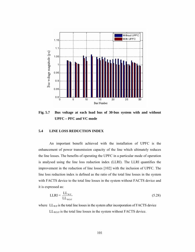
101
Fig. 5.7 Bus voltage at each load bus of 30-bus system with and without
UPFC – PFC and VC mode
5.4 LINE LOSS REDUCTION INDEX
An important benefit achieved with the installation of UPFC is the
enhancement of power transmission capacity of the line which ultimately reduces
the line losses. The benefits of operating the UPFC in a particular mode of operation
is analysed using the line loss reduction index (LLRI). The LLRI quantifies the
improvement in the reduction of line losses [102] with the inclusion of UPFC. The
line loss reduction index is defined as the ratio of the total line losses in the system
with FACTS device to the total line losses in the system without FACTS device and
it is expressed as:
W/F
WO/F
LLLLRI = LL
(5.28)
where LLW/F is the total line losses in the system after incorporation of FACTS device
LLWO/F is the total line losses in the system without FACTS device.

102
Based on the above definition, the following attributes are considered:
LLRI < 1: FACTS device has reduced line losses
LLRI = 1: FACTS device has no impact on system line losses
LLRI > 1: FACTS device is not beneficial.
The reduction in line losses is evident after connecting FACTS device which
is depicted in Table 5.2. It indicates the reduction in line losses with the installation
of UPFC for various cases. The line loss for the base case without UPFC installation
is calculated by load flow solutions and is found to be 7.616 MW. The line loss
reduction is indicated by means of LLRI and a maximum reduction of 23.68% is
obtained when the UPFC is operated in the simultaneous voltage and power flow
control mode.
Table 5.2 Line loss reduction results for various cases
Cases Line loss (MW) LLRI % Reduction
Base case 7.616 - -
Case I 6.237 0.8189 18.1
Case II 7.038 0.9241 7.58
Case III 5.812 0.7631 23.68
5.5 SUMMARY
The power flow algorithm has been built with the UPFC structure with the
view to enhance the system voltage and improve the power transfer capability of the
system. The proposed model has been evaluated through the standard IEEE 30-bus
power system. The role of UPFC in minimizing the line losses, besides enabling the
required reactive power support and augmenting the flow of real power over the line
has been illustrated.

103
CHAPTER 6
CONCLUSION
This chapter concludes the present work with a summary of research
contributions and explores the role of voltage source inverter configurations and
PWM techniques while integrating the FACTS devices into power systems.
The construction of new transmission lines has adverse impact on the
environment. FACTS devices help to distribute the electrical energy more
economically through better utilization of existing installation, thereby reducing the
need for additional transmission lines. They provide high quality electricity supply
including constant voltage and frequency which is the mandatory requirement for
modern industries. Besides, the application of FACTS in electric power system is
intended for reactive power compensation, control of active power flow, voltage
profile management, power factor correction and loss minimization. Among the
various FACTS controllers (SVC, TCSC, STATCOM, SSSC, UPFC), the devices
that use a dc-ac inverter are considered superior to those of phase controlled devices
in terms of harmonic performance, dynamic response and ease of operation. Hence
investigations in this work are directed to improve the performance of the VSI based
FACTS devices in a practical power system.
6.1 RESEARCH CONTRIBUTIONS
A novel structure has been suggested for UPFC, with a view to eliminate the
need for dc link capacitor. The front end converter has been operated through a
relatively new PWM scheme that enabled to regulate the dc link voltage, minimize
the ripples and improve the shape of the dc link current. The performance of the
proposed scheme has been analysed through MATLAB based simulation assuming
that the UPFC is inserted in a 230 kV transmission line of a sample power system.

104
It is inferred from the simulation results that the STATCOM offers a good voltage
regulation and SSSC controls the magnitude and angle of the series injected voltage
in order to maintain the real and reactive power over the transmission line to follow
the set reference values inspite of variations in the load and operating conditions.
Another scheme of UPFC has been explored in which the classical ac/dc and
dc/ac converter structure with dc link capacitor is replaced by a matrix converter.
The indirect space vector modulation technique has been effectively used to generate
the control pulses for the MC switches. The MC with its ability to exercise control
over the input current and/or the output voltage is preferred in UPFC structure since
a single control strategy can perform the control of the input current displacement
angle (for maintaining unity power factor) and series injected voltage, in order to
maintain the desired flow of power. The proposed schemes of UPFC interfaced in
the system accomplish a similar performance as that of a traditional system with dc
link capacitor.
A combined multipulse-multilevel inverter topology has been proposed for
STATCOM and SSSC applications. The performance of this inverter topology is
evaluated through MATLAB based simulation. The analytic expressions for the
proposed inverter topology have been derived using Fourier series. It is observed
that the theoretical results coincide closely with the simulated results. This new
configuration generates a premium quality three-phase sinusoidal voltage and
maintains THD well below 4%.
A static synchronous compensator has been realized using the proposed high
performance, reliable, flexible and cost effective inverter topology. A closed loop
control based on decoupled control strategy has been developed and found to be
effective over a wide range of power system operating conditions.
The combined multipulse-multilevel inverter has been operated suitably to
depict the behaviour of SSSC. A closed loop fuzzy logic control scheme has been
developed for operating the SSSC in the automatic power flow control mode. The
105
parameters of the FLC have been widely varied by a suitable choice of the
membership functions and parameters in the rule base. It is inferred from the results
that the FLC is a viable controller for the SSSC in order to maintain the real and
reactive power flow over the transmission line to follow the set reference values
under a variety of transient disturbances including high and low load conditions.
The computation and control of power flow for system embedded with
UPFC is a necessary requirement in the present day automated world to provide a
scope for effective planning and operation. It is in this context the power flow
algorithm has been developed with the UPFC structure. The proposed model has
been evaluated through the standard IEEE 30-bus power system. The role of UPFC
in minimizing the line losses, besides enabling the required reactive power support
and augmenting the flow of real power has been illustrated.
Since the dc link capacitor present in UPFC structure has inherent
disadvantages such as more space requirement, limited life and also expensive,
attempts has been made to overcome these issues. Further a new inverter
configuration with a very less harmonic component has been proposed for
integrating the shunt and series FACTS devices into power system. Also power
flow modeling and analysis of the UPFC which inherits the features of STATCOM
and SSSC have been done with a view to highlight its ability as a powerful voltage
regulator and a power controller.
6.2 SCOPE FOR FURTHER WORK
There are several interesting open problems while integrating power
electronic converters into power grid requiring further study. Some of them are
discussed here in brief.
The proposed inverter configuration can be employed to realize other
recently budding FACTS devices such as C-UPFC, G-UPFC, interline power flow
controller etc., All the investigations in this thesis are focused on the analysis of

106
STATCOM in the automatic voltage control mode and SSSC in the automatic power
flow control mode though it is pointed out that other operating modes such as
voltage injection mode, impedance control mode are possible. It will be interesting
to study the performance of the FACTS devices in other possible operating modes.
The parameters of the PI controllers used in the closed loop control scheme are
tuned using trial and error procedure. Instead artificial intelligence techniques such
as genetic algorithm or fuzzy neural network controllers may be employed to tune
the parameters of the PI controllers.

107
APPENDIX - A
Table A1 System Parameters in which UPFC Connected
Power system parameters Values
Rated voltage 230 kV
Frequency 50 Hz
SC level 10,000 MVA
Base voltage 230 kV
Three phase ac source
X/R 8
Resistance per unit length 0.01755 ohms/km
Inductance per unit length 0.8737 mH/km
Capacitance per unit length 13.33 nF/km
Transmission line
Line length 180 km
Nominal power 100 MVA
Frequency 50 Hz
Primary voltage 230 kV
Secondary voltage 25 kV
Magnetization resistance 500 pu
Shunt Transformer
Magnetization reactance 500 pu
Rated voltage 42 kV/14 kV
Rated power 70 MVA
Magnetization resistance 200 pu
Series Transformer
Magnetization reactance 800 pu
Internal resistance 0.001 Ω
Snubber resistance 0.1 MΩ IGBT switches
Snubber capacitance Infinite

108
APPENDIX – B
Table B1 Matrix Converter Switching Table
Group No. A B C ABV BCV CAV aI bI cI ON Switches
1 a b c abV bcV caV AI BI CI SAa SBb SCc
2 a c b caV− bcV− abV− AI CI BI SAa SBc SCb
3 b a c abV− caV− bcV− BI AI CI SAb SBa SCc
4 b c a bcV caV abV CI AI BI SAb SBc SCa
5 c a b caV abV bcV BI CI AI SAc SBa SCb
I
6 c b a bcV− abV− caV− CI BI AI SAc SBb SCa
1 a c c caV− 0 caV AI 0 AI− SAa SBc SCc
2 b c c bcV 0 bcV− 0 AI AI− SAb SBc SCc
3 b a a abV− 0 abV AI− AI 0 SAb SBa SCa
4 c a a caV 0 caV− AI− 0 AI SAc SBa SCa
5 c b b bcV− 0 bcV 0 AI− AI SAc SBb SCb
II-A
6 a b b abV 0 abV− AI AI− 0 SAa SBb SCb
1 c a c caV caV− 0 BI 0 BI− SAc SBa SCc
2 c b c bcV− bcV 0 0 BI BI− SAc SBb SCc
3 a b a abV abV− 0 BI− BI 0 SAa SBb SCa
4 a c a caV− caV 0 BI− 0 BI SAa SBc SCa
5 b c b bcV bcV− 0 0 BI− BI SAb SBc SCb
II-B
6 b a b abV− abV 0 BI BI− 0 SAb SBa SCb
1 c c a 0 caV caV− CI 0 CI− SAc SBc SCa
2 c c b 0 bcV− bcV 0 CI CI− SAc SBc SCb
3 a a b 0 abV abV− CI− CI 0 SAa SBa SCb
4 a a c 0 caV− caV CI− 0 CI SAa SBa SCc
5 b b c 0 bcV bcV− 0 CI− CI SAb SBb SCc
II-C
6 b b a 0 abV− abV CI CI− 0 SAb SBb SCa
1 a a a 0 0 0 0 0 0 SAa SBa SCa2 b b b 0 0 0 0 0 0 SAb SBb SCb
III
3 c c c 0 0 0 0 0 0 SAc SBc SCc

109
APPENDIX-C
Table C1 System Parameters in which SSSC Connected
Parameters Values
Rated Voltage 230 kV
MVA SC 10×103 MVA
Resistance 0.1 pu
Reactance 0.3 pu
Base Voltage 230 kV
Transmission line XL 0.25 pu
Transmission line RL 0.05 pu
DC Voltage 1 kV
Capacitance 750 μF
Series Transformer-Rated Voltage 6.6 kV/48 kV
Series Transformer-Rated Power 70 MVA

110
APPENDIX-D
The one line diagram of an IEEE 30-bus system is shown in Fig.D.1. The
line data and bus data are given in Table D.1 and D.2 respectively. The data is on
100 MVA base.
Fig. D.1 One line diagram of IEEE 30-bus system

111
Table D1 Line Data of IEEE 30-Bus System
Bus E Bus B R pu
X pu
1/2 B pu Line Code
1 2 0.0192 0.0572 0.02640 1 1 3 0.0452 0.1852 0.02040 1 2 4 0.0570 0.1737 0.01840 1 3 4 0.0132 0.0379 0.00420 1 2 5 0.0472 0.1983 0.02090 1 2 6 0.0581 0.1763 0.01870 1 4 6 0.0119 0.0414 0.00450 1 5 7 0.0460 0.1160 0.01020 1 6 7 0.0267 0.0820 0.00850 1 6 8 0.0120 0.0420 0.00450 1 6 9 0.0000 0.2080 0.00000 0.978 6 10 0.0000 0.5560 0.00000 0.969 9 11 0.0000 0.2080 0.00000 1 9 10 0.0000 0.1100 0.00000 1 4 12 0.0000 0.2560 0.00000 0.932 12 13 0.0000 0.1400 0.00000 1 12 14 0.1231 0.2559 0.00000 1 12 15 0.0662 0.1304 0.00000 1 12 16 0.0945 0.1987 0.00000 1 14 15 0.2210 0.1997 0.00000 1 16 17 0.0824 0.1923 0.00000 1 15 18 0.1073 0.2185 0.00000 1 18 19 0.0639 0.1292 0.00000 1 19 20 0.0340 0.0680 0.00000 1 10 20 0.0936 0.2090 0.00000 1 10 17 0.0324 0.0845 0.00000 1 10 21 0.0348 0.0749 0.00000 1 10 22 0.0727 0.1499 0.00000 1 21 22 0.0116 0.0236 0.00000 1 15 23 0.1000 0.2020 0.00000 1 22 24 0.1150 0.1790 0.00000 1 23 24 0.1320 0.2700 0.00000 1 24 25 0.1885 0.3292 0.00000 1 25 26 0.2544 0.3800 0.00000 1 25 27 0.1093 0.2087 0.00000 1 28 27 0.0000 0.3960 0.00000 0.968 27 29 0.2198 0.4153 0.00000 1 27 30 0.3202 0.6027 0.00000 1 29 30 0.2399 0.4533 0.00000 1 8 28 0.0636 0.2000 0.0214 1 6 28 0.0169 0.0599 0.065 1
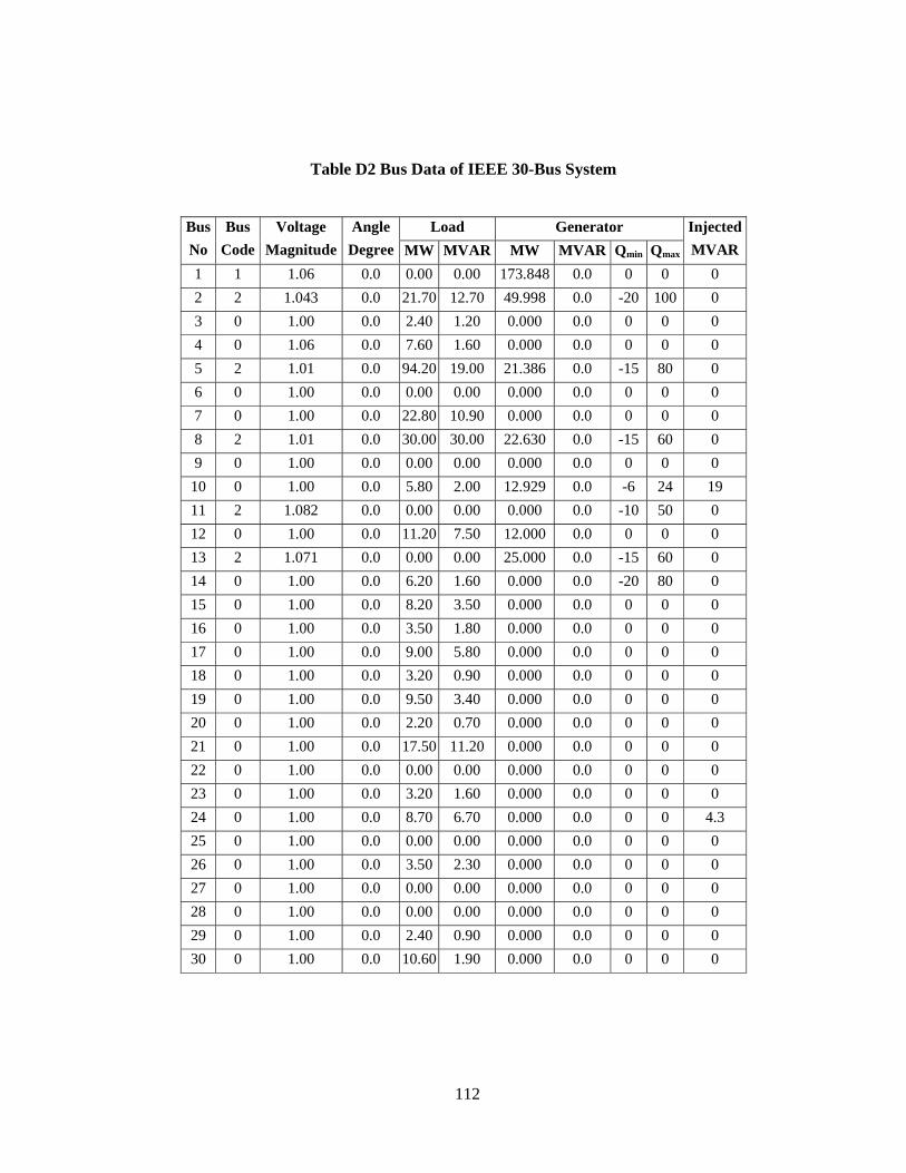
112
Table D2 Bus Data of IEEE 30-Bus System
Load Generator Bus No
Bus Code
Voltage Magnitude
Angle Degree MW MVAR MW MVAR Qmin Qmax
Injected MVAR
1 1 1.06 0.0 0.00 0.00 173.848 0.0 0 0 0 2 2 1.043 0.0 21.70 12.70 49.998 0.0 -20 100 0 3 0 1.00 0.0 2.40 1.20 0.000 0.0 0 0 0 4 0 1.06 0.0 7.60 1.60 0.000 0.0 0 0 0 5 2 1.01 0.0 94.20 19.00 21.386 0.0 -15 80 0 6 0 1.00 0.0 0.00 0.00 0.000 0.0 0 0 0 7 0 1.00 0.0 22.80 10.90 0.000 0.0 0 0 0 8 2 1.01 0.0 30.00 30.00 22.630 0.0 -15 60 0 9 0 1.00 0.0 0.00 0.00 0.000 0.0 0 0 0 10 0 1.00 0.0 5.80 2.00 12.929 0.0 -6 24 19 11 2 1.082 0.0 0.00 0.00 0.000 0.0 -10 50 0 12 0 1.00 0.0 11.20 7.50 12.000 0.0 0 0 0 13 2 1.071 0.0 0.00 0.00 25.000 0.0 -15 60 0 14 0 1.00 0.0 6.20 1.60 0.000 0.0 -20 80 0 15 0 1.00 0.0 8.20 3.50 0.000 0.0 0 0 0 16 0 1.00 0.0 3.50 1.80 0.000 0.0 0 0 0 17 0 1.00 0.0 9.00 5.80 0.000 0.0 0 0 0 18 0 1.00 0.0 3.20 0.90 0.000 0.0 0 0 0 19 0 1.00 0.0 9.50 3.40 0.000 0.0 0 0 0 20 0 1.00 0.0 2.20 0.70 0.000 0.0 0 0 0 21 0 1.00 0.0 17.50 11.20 0.000 0.0 0 0 0 22 0 1.00 0.0 0.00 0.00 0.000 0.0 0 0 0 23 0 1.00 0.0 3.20 1.60 0.000 0.0 0 0 0 24 0 1.00 0.0 8.70 6.70 0.000 0.0 0 0 4.3 25 0 1.00 0.0 0.00 0.00 0.000 0.0 0 0 0 26 0 1.00 0.0 3.50 2.30 0.000 0.0 0 0 0 27 0 1.00 0.0 0.00 0.00 0.000 0.0 0 0 0 28 0 1.00 0.0 0.00 0.00 0.000 0.0 0 0 0 29 0 1.00 0.0 2.40 0.90 0.000 0.0 0 0 0 30 0 1.00 0.0 10.60 1.90 0.000 0.0 0 0 0

113
REFERENCES
[1] L. Gyugyi and N. G. Hingorani, “Understanding FACTS: Concepts and
Technology of Flexible AC Transmission Systems”, IEEE press, New York,
1999.
[2] L. Gyugyi, “Unified power-flow control concept for flexible AC transmission
systems”, IEE Proceedings-C, Vol.139, pp.323-331, No.4, July 1992.
[3] Y. H. Song and A. Johns, “Flexible AC transmission systems (FACTS)”,
IEE Power and Energy series 30, London, UK, 1999.
[4] R.M.Mathur and R.K.Varma, “Thyristor based FACTS controllers for
Electrical transmission systems”, Wiley-Interscience, 2002.
[5] B.A. Renz, A. Keri, A.S.Mehraban, C.Schauder, E.Stacey, L.Kovalsky, L.Gyugyi
and A.Edris, “AEP Unified power flow controller performance”, IEEE
Transactions on Power Delivery, Vol.14, No.4, pp.1374-1381, October 1999.
[6] EPRI Report on Flexible AC Transmission Systems (FACTS), Number
EL-6943, September 1991.
[7] T.J.E.Miller, “Reactive power control in Electric systems”, John Wiley and
Sons, 1982.
[8] R.A.Otto, T.H.Putman and L.Gyugyi, “Principles and applications of static,
Thyristor controlled shunt compensators”, IEEE Transactions on Power
Apparatus and Systems, Vol. PAS-97, No.5, pp.1935-1945, September 1978.
[9] Canizares.C.A and Faur.Z.T, “Analysis of SVC and TCSC controllers in
voltage collapse”, IEEE Transactions on Power Systems, Vol.14, No.1,
pp.158-165, February 1999.

114
[10] San-YiLee, Chi-Jui Wu, and Wei-Nan Chang, “A compact control algorithm
for reactive power compensation and load balancing with static VAR
compensator”, Electric Power Systems Research, Elsevier, Vol. 58, No.2,
pp.63-70, June 2001.
[11] J.J.Paserba, N.W.Miller, E.V.Larsen and R.J.Piwko, “A thyristor controlled
series compensation model for power system stability analysis”, IEEE
Transactions on Power Delivery, Vol.10, No.3, pp.1471-1478, July 1995.
[12] Sameh K.M. Kodsi, Claudio A. Canizares and Mehrdad Kazerani, “Reactive
current control through SVC for load power factor correction”, Electric Power
Systems Research, Elsevier, Vol.76, No. 9-10, pp.701-708, June 2006.
[13] L.Gyugyi, “Application characteristics of converter based FACTS
controllers”, Proceedings of POWERCON 2000, Piscataway, New Jercy,
Vol.1, pp.391-396, 2000.
[14] L. Gyugyi, “Dynamic compensation of AC transmission lines by solid state
synchronous voltage sources”, IEEE Transactions on Power Delivery, Vol.9,
No.2, pp.904–911, April 1994.
[15] C.Schauder, M.Gemhardt, E.Stancey, T.Lemak, L.Gyugyi, T.W. Cease and
A.Edris, “Development of a ±100MVAR static condenser for voltage control
of transmission systems”, IEEE Transactions on Power Delivery, Vol.10,
No.3, pp.1486-1496, July 1995.
[16] L.Xu, V.G.Agelidis and E.Acha, “Development considerations of
DSP-controlled PWM VSC-based STATCOM”, IEE Proceedings-Electrical
Power Application, Vol.148, No.5, pp.449-455, September 2001.
[17] L. Gyugyi, C.D.Schauder and Kalyan K. Sen, “Static Synchronous Series
Compensator: A Solid State Approach to the series compensation of
transmission line”, IEEE Transactions on Power Delivery, Vol.12, No.1,
pp.406-417, January 1997.

115
[18] Kalyan K. Sen, “SSSC - Static Synchronous Series Compensator: Theory,
Modeling and Applications”, IEEE Transactions on Power Delivery, Vol.13,
No.1, pp.241-246, January 1998.
[19] Fawzi A. Rahman, Al Jowder and Boon-Teck Ooi, “Series Compensation of
Radial Power System by a Combination of SSSC and Dielectric Capacitors”,
IEEE Transactions on Power Delivery, Vol.20, No.1, pp.458-465, January 2005.
[20] L.Gyugyi, C.D.Schauder, S.L.William, T.R. Rietman, D.R.Torgersona and
A.Edris, “The unified power flow controller: A new approach to power
transmission control”, IEEE Transactions on Power Delivery, Vol.10, No.2,
pp.1085-1097, April 1995.
[21] K.K. Sen and E.J.Stacey, “UPFC-Unified power flow controllers, Theory,
Modeling and Applications”, IEEE Transactions on Power Delivery, Vol.13,
No.4, pp.1453-1460, October 1998.
[22] A.J.F.Keri, “Unified power flow controller (UPFC): Modeling and analysis”,
IEEE Transactions on Power Delivery, Vol.14, No.2, pp.648-654, April 1999.
[23] P.Kumkratug and M.H.Haque, “Versatile model of a unified power flow
controller in a simple power system”, IEE Proceedings-Generation,
Transmission and Distribution, Vol.150, No.2, pp.155-161, March 2003.
[24] C.D. Schauder, L.Gyugyi, M.R. Lund, F.M. Hamai, T.R. Rietman,
D.R.Torgerson and A.Edris, “Operation of the unified power flow controller
under practical constraints”, IEEE Transactions on Power Delivery, Vol.13,
No.2, pp.630-639, 1998.
[25] Math H.J.Bollen, “Understanding power quality problems: voltage sags and
interruptions”, IEEE Press, Piscataway, New Jercy, USA, 2000.
[26] Canadian Electrical Association, “Static compensator for reactive power
control”, Cantext Publications, 1984.

116
[27] Sang Y. Lee, Subroto Bhattacharya, Tommy Lejonberg, Adel Hammad and
Serge Lefebvre, “Detailed Modeling of Static Var Compensators using the
Electromagnetic Transients Program (EMTP)”, IEEE Transactions on Power
Delivery, Vol.7. No.2, pp.836-847, April 1992.
[28] K.A.Ellithy and S.M.Al-Alwai, “Tuning a static var compensator controller
over a wide range of load models using an artificial neural network”, Electric
Power Systems Research, Elsevier, Vol.38, No.2, pp.97-104, August 1996.
[29] J.Urbanek, R.J.Piwko, E.V.Larsen, B.L.Damsky, B.C.Furumasu,
W.Mittlestadt, and J.D.Edan, “Thyristor controlled series compensation
prototype installation at the Slatt 500kV substation”, IEEE Transactions on
Power Delivery, Vol.8, No.3, pp.1460-1469, July 1993.
[30] Y.Sumi, Y.Harumoto, T.Hasegawa, M.Yano, K.Ikeda and T.Matsura, “New
static var control using forced commutated inverters”, IEEE Transactions of
Power Apparatus and Systems, Vol.PAS-100, No.9, pp.4216-4226,
September 1981.
[31] S.Mori, K.Matsuno, T.Hasegawa, S.Ohnishi, M.Takeda, M.Seto, S.Murakani
and F.Ishiguro, “Development of a large static var generator using self
commutated inverters for improving power system stability”, IEEE
Transactions on Power Systems, Vol.8, No.1, pp.371-377, February 1993.
[32] K.K. Sen and E.J.Stacey, “UPFC-Unified power flow controllers, Theory,
Modeling and Applications”, IEEE Transactions on Power Delivery, Vol.13,
No.4, pp.1453-1460, October 1998.
[33] A.J.F.Keri, “Unified power flow controller (UPFC): Modeling and analysis”,
IEEE Transactions on Power Delivery, Vol.14, No.2, pp.648-654, April 1999.
[34] I.Papic, “Mathematical analysis of FACTS devices based on a voltage source
converter. Part I. Mathematical models”, Electric Power Systems Research,
Elsevier, Vol.56, pp.139-148, 2000.

117
[35] I.Papic, “Mathematical analysis of FACTS devices based on a voltage source
converter. Part II. Steady state operational characteristics”, Electric Power
Systems Research, Elsevier, Vol.56, pp.149-157, 2000.
[36] Amit Jain, Karan Joshi, Aman Behal and Ned Mohan, “Voltage regulation
with STATCOMs: Modeling, Control and Results”, IEEE Transactions on
Power Delivery, Vol.21, No.2, pp.726-735, April 2006.
[37] L.Sunil Kumar and Arindam Ghosh, “Modeling and control design of a static
synchronous series compensator”, IEEE Transaction on Power delivery,
Vol.14, No.4, pp.1448-1453, October 1999.
[38] T.Makombe and N.Jenkins, “Investigation of a unified power flow
controller”, IEE Proceedings on Generation, Transmission and Distribution,
Vol.146, No.4, pp.400-408, July 1998.
[39] Z. Huang, Y. Ni, C.M. Shen, F.F. Wu, S.Chen and B. Zhang, “Application of
unified power flow controller in interconnected power systems- modeling,
interface, control strategy and case study”, IEEE Transaction on Power
Systems, Vol.15, No.2, pp.817-824, May 2000.
[40] Kalyan K. Sen and Eric J. Stacey, “UPFC - Unified Power Flow Controller:
Theory, Modeling, and Applications”, IEEE Transactions on Power
Delivery, Vol.13, No.4, pp.1453-1460, October 1998.
[41] X.Lombard and P.G.Therond, “Control of unified power flow controller:
Comparison of methods on the basis of a detailed numerical model”, IEEE
Transactions on Power Systems, Vol.12, No.2, pp.824-830, May 1997.
[42] S.A. Al-Mawsawi, “Comparing and evaluating the voltage regulation of a
UPFC and STATCOM”, Electric Power and Energy Systems, Elsevier,
Vol.25, pp.735-740, 2003.

118
[43] Dong-Jun Won, Il-Yop Chung and Seung-Il Moon, “Determination of
equivalent impedances of UPFC voltage-source model from the dynamic
responses of UPFC switching-level model”, Electric Power and Energy
Systems, Elsevier, Vol.25, pp.463-470, 2003.
[44] M.Imayavaramban, K.Latha and G.Uma, “Analysis of different schemes of
matrix converter with maximum voltage conversion ratio”, Proceedings of
IEEE MELECON 2004, Croatia, pp.1137-1140, May 2004.
[45] Lixiang Wei, Yoichi Matsushita and Thomas A. Lipo, “A compensation
method for Dual-bridge matrix converters operating under distorted source
voltages”, Proceedings of IEEE Power Electronic Specialist Conference,
PESC’ 2003, Mexico, pp.2078-2083, 2003.
[46] Kenichi Iimori, Katsuji Shinohara, Mitsuhiro Muroya and Yoichi
Matsushita, “Zero-Switching-Loss PWM Rectifier of Converter without dc
Link Components for Induction Motor Drive”, Proceedings of IEEE Power
Conversion Conference, PCC-2002, OSAKA, pp.1-6, April 2002.
[47] Kenichi Limori, Katsuji Shinohara, Muroya and Kitanaka HideToshi,
“Characteristics of new current controlled PWM rectifier-voltage source inverter
without dc link components for Induction motor drive”, Transactions of the
Institute of Electrical Engineers of Japan, Vol.119D, No.2, pp.133-141, 1999.
[48] Kenichi Iimori, Katsiji Shinohara and Kichiro Yamamoto, “A study of dead
time of PWM rectifier of voltage source inverter without dc link components
and its operating characteristics of Induction motor”, Proceedings of Industry
Application Conference, Seattle, Vol.3, pp.1638-1646, October 2004.
[49] Fang Zheng Peng, Lihuna Chen and Fan Zhang, “Simple topologies of PWM
AC-AC converters”, IEEE Transactions on Power Electronics Letters, Vol.1,
No.1, pp.10-13, March 2003.

119
[50] Y. Minari, K. Shinohara and R.Veda, “PWM-rectifier/voltage-source
inverter without dc link components for induction motor drive”, IEE
Proceedings –B, Vol.140, No.6, pp.363-367, November 1993.
[51] Alberto Alesina and Marco G.B.Venturini, “Analysis and design of optimum
amplitude nine switch direct AC-AC converters”, IEEE Transactions on
Power Electronics, Vol.4, No.1, pp.101-112, January 1989.
[52] S.H.Hosseini and E.Babaei, “A new generalized direct matrix converter”,
Proceedings of IEEE International Symposium, ISIE 2001, Pusan, Vol.2,
pp.1071-1076, June 2001.
[53] Feng Liu, Shengwei Mei, Qiang Lu, Yixin Ni, Felix F.Wu and Akihiko
Yokoyama, “The nonlinear internal control of STATCOM: theory and
application”, Electric Power and Energy systems, Elsevier, Vol.25, pp.421-430,
2003.
[54] N.C.Sahoo, B.K.Panigrahi, P.K.Dash and G.Panda, “Multivariable nonlinear
control of STATCOM for synchronous generator stabilization”, Electric
Power and Energy Systems, Elsevier, Vol.26, pp.37-48, 2004.
[55] Anil. C. Pradhan and P.W. Lehn, “Frequency domain analysis of the static
synchronous series compensator”, IEEE Transactions on Power Delivery,
Vol.21, No.1, pp. 440-450, January 2006.
[56] Yang Ye and Mehrdad Kazerani, “Power flow control schemes for series
connected FACTS controllers”, Electric Power Systems Research, Elsevier,
Vol.76, pp.824-831, 2006.
[57] Diego Soto and Tim.C. Green, “A comparison of High-Power Converter
Topologies for the implementation of FACTS Controllers”, IEEE Transactions on
Industrial Electronics, Vol.49, No.5, pp.1072-1080, October 2002.

120
[58] Bhim Singh, G. Bhuvaneswari and Vipin Garg, “Harmonic mitigation using
12-pulse ac-dc converter in Vector Controlled Induction Motor Drives”, IEEE
Transactions on Power Delivery, Vol.21, No.3, pp.1483-1492, July 2006.
[59] Ricardo Davalos M., Juan M. Ramirez and O. Ruben Tapia, “Three-phase
multi-pulse converter STATCOM analysis”, Electric Power and Energy
Systems, Elsevier, Vol.27, pp.39-51, 2005.
[60] Bhim Singh and R. Saha, “A New 24-Pulse STATCOM for voltage
regulation”, Proceedings of International Conference on Power Electronics,
Drives and Energy Systems, PEDES 2006, New Delhi, India, 8B-03, 2006.
[61] Pavel Zuniga-Haro and Juan M.Ramirez, “Static synchronous series compensator
operation based on 48-pulse VSC”, Proceedings of the 37th Annual North
American Power Symposium, Mexico, pp.102-109, October 2005.
[62] A. Nabae, Akira Takahashi, Isao Akagi and Hirofumi, “A new neutral point
clamped PWM inverter”, IEEE Transactions on Industry Applications,
Vol.IA-7, No.5, pp.518-523, September 1981.
[63] X.Yuan and I.Barbi, “Fundamentals of a new diode clamping multilevel
inverter”, IEEE Transactions on Power Electronics, Vol.15, No.4,
pp.711-718, July 2002.
[64] J.S.Lai and F.Z.Peng, “Multilevel converters – A new breed of power
converters”, IEEE Transactions on Industrial Applications, Vol.32,
pp. 509-517, May/June 1996.
[65] F.G.Peng and J.S.Lai, “Multilevel cascade voltage source inverter with
separate dc sources”, U.S. Patent 5 642 275, June 24, 1997.
[66] J. Rodriguez, J.S.Lai and F.Z.Peng, “Multilevel inverters: A survey of
topologies, controls and applications”, IEEE Transactions on Industrial
Electronics, Vol.49, No.4, pp.724-738, August 2002.

121
[67] F.Z.Peng, J.S.Lai, J.W.McKeever and J.A.Vancoevering, “Multilevel voltage
source inverter with separate dc sources for static var generation”, IEEE
Transactions on Industrial Applications, Vol.32, No.5, pp.1130-1138,
September/October 1996.
[68] B.T.Ooi, G.Joos and X.Huang, “Operating principles of shunt STATCOM
based on 3-level diode clamped converters”, IEEE Transactions on Power
Delivery, Vol.14, No.4, pp.1504-1510, October 1999.
[69] F.Z.Peng and J.S.Lai, “Dynamic performance and control of a static var
generator using cascade multilevel inverters”, IEEE Transactions on
Industrial Applications, Vol.33, No.3, pp.748-755, May/June 1997.
[70] Li-Xin Wang, “A course in Fuzzy system and control”, Prentice Hall,
Englewood Cliffs, NJ, 1997.
[71] J.A.Momoh, X.W.Ma and K.Tomsovic, “Overview and literature survey of
Fuzzy set theory in power systems”, IEEE Transactions on Power systems,
Vol.10, No.3, pp.1676-1690, August 1995.
[72] Ahad Kazemi and Mahmoud Vakili Sohrforouzani, “Power system damping
using fuzzy controlled FACTS devices”, Electric Power and Energy
Systems, Elsevier, Vol.28, pp.349-357, November 2006.
[73] L.O.Mak, Y.X.Ni and C.M. Shen, “STATCOM with fuzzy controllers for
interconnected power systems”, Electric Power Systems Research, Elsevier,
Vol.55, pp.87-95, 2000.
[74] Stella Morris, P.K.Dash and K.P.Basu, “A fuzzy variable structure controller for
STATCOM”, Electric Power Systems Research, Elsevier, Vol.65, pp.23-34,
2003.

122
[75] B.N.Singh, A.Chandra, K.Al-Haddad and B.Singh, “Performance of sliding
mode and fuzzy controllers for a static synchronous series compensator”,
IEE – Proceedings on Generation, Transmission and Distribution, Vol.146,
No.2, pp.200-206, March 1999.
[76] S.Kannan, S.Jayaram and M.M.A. Salama, “Fuzzy logic based
supplementary controller for static synchronous series compensator”,
Proceedings of the IEEE Canadian Conference on Electrical and Computer
Engineering, Waterloo, Vol.2, pp.489-492, May 1998.
[77] V.K.Chandrakar and A.G.Kothari, “Fuzzy logic based static synchronous
series compensator (SSSC) for transient stability improvement”, Proceedings
of IEEE International conference on Electric Utility, Deregulation,
Restructuring and Power Technologies, DRPT 2004, Hongkong,
pp.240-245, April 2004.
[78] Fang Wangliang and H.W.Nagan, “A robust load flow technique for use in
power systems with unified power flow controllers”, Electric Power Systems
Research, Elsevier, Vol.53, No.3, pp.181-186, 2000.
[79] Prasad Padhy Narayana and M.A.Abdel Moamen, “Power flow control and
solutions with multiple and multi-type FACTS devices”, Electric Power
Systems Research, Elsevier, Vol.74, No.3, pp.341-351, 2005.
[80] Mihalic R.Zunko and D.Povh, “Improvement of transient stability using
unified power flow controller”, IEEE Transactions on Power Delivery,
Vol.11, No.1, pp.485-492, January 1996.
[81] H.Ambrez Perez, E.Acha, C.R.Fuerte-Esquivel, A.De la Torre,
“Incorporation of a UPFC model in an optimal power flow using Newton’s
method”, IEE Proceedings on Generation, Transmission and Distribution,
Vol.145, No.3, pp.336-344, 1998.

123
[82] Ghadir Radman and Reshma S.Raje, “Power flow model/calculation for
power systems with multiple FACTS controllers”, Electric Power Systems
Research, Elsevier, Vol.77, pp.1521-1531, 2007.
[83] Y.H.Song, J.Y.Liu and P.A.Mehta, “Power injection modeling and optimal
multiplier power flow algorithm for steady state studies of unified power
flow controllers”, Electric Power Systems Research, Elsevier, Vol.52, No.3,
pp.51-59, September 1999.
[84] A.Mete Vural and Mehmet Tumay, “Mathematical modeling and analysis of
a unified power flow controller: A comparison or two approaches in power
flow studies and effects of UPFC location”, Electric Power and Energy
Systems, Elsevier, Vol.29, No.8, pp.617-629, October 2007.
[85] J.S. Kim and S.K. Sul, “New control scheme for ac-dc-ac converter without
dc-link electrolytic capacitor”, Proceedings of IEEE Power Electronic
Specialist Conference, PESC’93, Seattle, pp.300-306, 1993.
[86] Mino K, Okuma Y and Kuroki K, “Direct-linked type frequency changer
based on dc clamped bilateral switching circuit topology”, IEEE
Transactions on Industry Applications, Vol.34, No.6, pp.1309-1317,
November/December 1998.
[87] Kyo-Beum Lee and Frede Blaabjerg, “A nonlinearity compensation method
for a matrix converter drive”, IEEE Power Electronics Letters, Vol.3, No.1,
pp.19-23, March 2005.
[88] Amir H.Norouzi and A.M.Sharaf, “A novel control scheme for the
STATCOM stability enhancement”, Proceedings of Transmission and
Distribution Conference and Exposition, Canada, Vol.1, pp.24-29,
September 2003.

124
[89] M.S.El.Moursi and A.M.Sharaf, “Novel controllers for the 48-pulse VSC
STATCOM and SSSC for voltage regulation and reactive power
compensation”, IEEE Transactions on Power Systems, Vol.20, No.4,
pp.1985-1997, November 2005.
[90] Macro Liserre, Antonio Dell Aquila and Frede Blaabjerg, “Genetic
Algorithm-Based Design on the Active damping for an LCL-Filter Three-
phase Active Rectifier”, IEEE Transactions on Power Electronics, Vol.19,
No.1, pp.76-86, January 2004.
[91] Boon-Teck Ooi and Mehrdad Kazerani, “Voltage source matrix converter as
a controller in Flexible AC Transmission Systems”, IEEE Transactions on
Power Delivery, Vol.13, No.1, pp.247-253, January 1998.
[92] S. Kim, S.K. Sul and T.A. Lipo, “AC/AC power conversion based on matrix
converter topology with unidirectional switches”, IEEE Transactions on
Industry Applications, Vol.36, No.1, pp.139-145, 2000.
[93] Lixiang. Wei and T. A. Lipo, “Matrix converter with reduced number of
switches”, Proceedings of IEEE Power Electronic Specialist Conference,
PESC 2002, Madison, Vol.1, pp.57-63, 2002.
[94] Laszld Huber and Dusan Borojevic, “Space vector modulation with unity
input power factor for forced commutated cycloconverters”, Proceedings of
the Conference on Industry Applications, Dearborn, USA, Vol.1,
pp.1032-1041, October 1991.
[95] D. Casadei, G.Grandi, G.Serra and A.Tani, “Space vector control of matrix
converters with unity input power factor and sinusoidal input/output
waveforms”, Proceedings of the Fifth European Conference on Power
Electronics and Applications, Brighton, Vol.7, pp.170-175, September 1993.

125
[96] Yidan Li and Bin Wu, “A novel dc voltage detection technique in the CHB
inverter-based STATCOM”, IEEE Transactions on Power Delivery, Vol.23,
No.3, pp.1613-1619, July 2008.
[97] D.J.Hanson, M.L.Woodhouse, C.Horwill, D.R.Monkhouse and
M.M.Osborne, “STATCOM: A new era of reactive compensation”, Power
Engineering Journal, Vol.16, No.3, pp.151-160, June 2002.
[98] T.Takagi and M.Sugeno, “Fuzzy identification of systems and its
applications to modeling and control”, IEEE Transactions on Systems, Man
and Cybernetics, Vol.15, No.1, pp.116-132, 1985.
[99] H.Akagi, Y.Kanazawa and A.Nabae, “Instantaneous reactive power
compensators comprising switching devices without energy storage
components”, IEEE Transactions on Industrial Applications, Vol.IA-20,
pp.625-631, 1984.
[100] K.S.Verma, S.N.Singh and H.D.Gupta, “Location of unified power flow
controller for congestion management”, Electric Power Systems Research,
Elsevier, Vol.58, pp.89-96, 2001.
[101] http://www.ee.washington.edu/research/pstca/pf30/pg_tca30bus.htm
[102] Ajay D.Vimalraj, S.Senthilkumar, J.Raja, S.Ravichandran and
T.G.Palanivelu, “Optimisation of distributed generation capacity for line loss
reduction and voltage profile improvement using PSO”, Journal of Electrical
Systems, ELEKTRIKA, Vol.10, No.2, pp.41-48, 2008.

126
LIST OF PUBLICATIONS
International Journals
1. “Investigation of performance of UPFC without dc link capacitor”, Electric
Power Systems Research, Elsevier, Vol. 78, No.4, pp.736-746, 2007.
2. “Fine tuning of cascaded of d-q axis controller for ac-dc-ac converter without dc
link capacitor using artificial neural network”, Songklanakalarin Journal of
Science and Technology, Vol.30, No.1, pp.85-92, January–February 2008.
3. “A fuzzy logic controller for enhancing the transient stability of 48-pulse
inverter based SSSC”, Journal of Electrical systems, ELEKTRIKA,
Universiti Teknologi Malaysia, Vol.10, No.2, pp.53-58, 2008.
4. “A combined multipulse – multilevel inverter based STATCOM for
improving the voltage profile and transient stability of power system”,
International Journal of Power Electronics, Inderscience (In Press).
International Conferences
1. “Comparing and evaluating the performance of SSSC with fuzzy logic
controller and PI controller for transient stability enhancement”,
Proceedings of 2006 IEEE India International Conference on Power
Electronics, IICPE 2006, Chennai, India, pp.140-143, 2006.
2. “Performance analysis of ac-dc-ac converter as Matrix converter”,
Proceedings of 2006 IEEE India International Conference on Power
Electronics, IICPE 2006, Chennai, India, pp.57 - 61, 2006.

127
3. “A current source rectifier with leading power factor”, Proceedings of IEEE
International Conference on Power Electronics, Drives and Energy
Systems, PEDES - 2006, New Delhi, 3A-20, 2006.
4. “An analytic approach to harmonic analysis of 48-Pulse voltage source inverter”,
Proceedings of 7th IEEE International Conference on Power Electronics and
Drive systems, PEDS 07, Bangkok, Thailand, pp.417-422, 2007.
5. “Dynamic Characteristic Analysis of SSSC Based on 48-Pulse Inverter”,
Proceedings of 8th IEEE International Power Engineering Conference,
IPEC 07, Singapore, pp.720-724, 2007.
6. “Performance evaluation of three phase cascaded H-bridge multilevel
inverter based on multi carrier PWM techniques”, Proceedings of IEEE
International Conference on Advances in Energy Research,
ICAER 2007, Mumbai, India, pp.537-542, 2007.
7. “A combined multipulse-multilevel voltage source inverter configuration for
STATCOM applications”, Proceedings of IEEE Power India Conference,
POWERCON 2008, New Delhi, pp.1-5, October 2008.

128
VITAE
B.Geethalakshmi was born in Chennai, India in 1974. She received her B.E
degree in Electronics and Communication Engineering and bagged gold medal from
Bharathidasan University, Tiruchirapalli, India in 1996. Also she received ME
degree in Power Electronics and Drives and bagged gold medal from the same
University in 1999. Presently she is working as Senior Lecturer in the Department of
Electrical and Electronics Engineering, Pondicherry Engineering College,
Pondicherry, India. She has published 15 papers in national and international
conference proceedings and journals, inclusive of the ones listed. Her area of interest
includes Power Converters and Power Electronic Applications in Power Systems.